advanced lithography 2019 call for...
TRANSCRIPT

AD
VAN
CE
D L
ITH
OG
RA
PH
Y C
ALL
FO
R P
AP
ER
S
www.spie.org/AL19call
24–28 February 2019San Jose Convention CenterSan Jose, California
CALL FORPAPERS
Advanced Lithography 2019
Submit abstracts by 29 August 2018

www.spie.org/AL19call
Conferences and Courses 24–28 February 2019
Exhibition 26–27 February 2019
San Jose Convention Center San Jose, California, USA
Submit abstracts by 29 August 2018
Share your research and make an impact in the semiconductor industry Present your work in optical lithography, metrology, or EUV. Share your latest advancements at the meeting where leaders come to network and solve lithography and patterning challenges in the semiconductor industry.

Symposium Chair:
The SPIE Advanced Lithography Symposium has been the showcase of the latest advances in lithography and patterning technology for over four decades. The 2019 symposium will cover the full spectrum of the advances and challenges in state-of-the art lithography technology through several topical conferences. Advances in areas of nano- and micro-patterning for semiconductor IC device application will be presented in sessions devoted to optical lithography, extreme-UV (EUV) lithography, metrology/inspection, patterning materials, etch/deposition technology, and process/technology optimization. As novel patterning and non-IC lithography technologies have become more widely explored, related topics in these areas are also addressed. This year’s symposium is structured into the following seven conferences, each organized by current practitioners of the art working together with organizing committees of experts in these fields.
This year joint sessions between the conferences will be aligned with several predefined “Topical Tracks” (for example: Machine Learning, stochastic effects, 3D device patterning,..) this will offer attendees the opportunity to cover important topics common across these interest areas and minimize topic presentation overlaps. Additionally, the Novel Patterning conference will expand to now include MEMS, NEMS and MEOMS and will include an invited session from industry leaders in this field.
The Advanced Lithography Symposium continues its role in bringing together the microlithography communities involved with semiconductor devices, micro-/nano-systems, and related fields. Participants come from a broad array of backgrounds to share and learn about state-of-the-art design, tools, materials, metrology, and process integration. Through a series of provocative panel discussions and seminars, the symposium also probes current issues being faced as we extend current methods, move toward alternative approaches, and identify new ways to complement one technology with another. The Symposium also provides the unique and primary forum for meeting and interacting with a wide range of industry experts, researchers, academics, and key players working on patterning technology development. Attendance ensures that participants learn and share the latest developments in areas of central importance to many vital technology fields.
We welcome your participation for the 2019 SPIE Advanced Lithography Symposium and urge you to submit your abstracts to the appropriate conference as described in the individual Calls for Papers, and be sure to encourage your colleagues to do the same. Relevant topics for new technology groups, keynote talks, or panel discussions are also solicited.
Will ConleyCymer—An ASML company(USA)
Plan to Participate
Kafai LaiIBM T.J. Watson Research Ctr. (USA)
Symposium Co-Chair:
AL101 Extreme Ultraviolet Lithography (EUV) X (Goldberg, Felix) . . . . . . . . . . . . . . . . . . . 3
AL102 Novel Patterning Technologies for Semiconductors, MEMS/NEMS, and MOEMS 2019 (Sanchez, Panning) . . . . . . . 4
AL103 Metrology, Inspection, and Process Control for Microlithography XXXIII (Ukraintsev, Adan) . . . . . . . . . . . . . . . . . . 5
AL104 Advances in Patterning Materials and Processes XXXVI (Gronheid, Sanders) . . . 7
AL105 Optical Microlithography XXXII (Kye, Owa) . . . . . . . . . . . . . . . . . . . . . . . . 8
AL106 Design-Process-Technology Co-optimization for Manufacturability XIII (Cain, Yuan) . . . . . . . . . . . . . . . . . . . . . . 10
AL107 Advanced Etch Technology for Nanopatterning VIII (Wise, Labelle) . . . . 11
Topical Tracks . . . . . . . . . . . . . . . . . . . . . . . . . . .12
Submission of Abstracts . . . . . . . . . . . . . . . . . .13
General Information . . . . . . . . . . . . . . . . . . . . . .15
Contents
2 SPIE ADVANCED LITHOGRAPHY 2019 • www.spie.org/AL19call
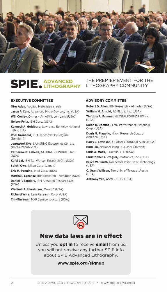
THE PREMIER EVENT FOR THE LITHOGRAPHY COMMUNITY
EXECUTIVE COMMITTEEOfer Adan, Applied Materials (Israel)
Jason P. Cain, Advanced Micro Devices, Inc. (USA)
Will Conley, Cymer – An ASML company (USA)
Nelson Felix, IBM Corp. (USA)
Kenneth A. Goldberg, Lawrence Berkeley National Lab. (USA)
Roel Gronheid, KLA-Tencor/ICOS Belgium (Belgium)
Jongwook Kye, SAMSUNG Electronics Co., Ltd. (Korea.Republic of)
Catherine B. Labelle, GLOBALFOUNDRIES Inc. (USA)
Kafai Lai, IBM T.J. Watson Research Ctr. (USA)
Soichi Owa, Nikon Corp. (Japan)
Eric M. Panning, Intel Corp. (USA)
Martha I. Sanchez, IBM Research – Almaden (USA)
Daniel P. Sanders, IBM Almaden Research Ctr. (USA)
Vladimir A. Ukraintsev, Qorvo™ (USA)
Richard Wise, Lam Research Corp. (USA)
Chi-Min Yuan, NXP Semiconductors (USA)
Robert D. Allen, IBM Research – Almaden (USA)
William H. Arnold, ASML US, Inc. (USA)
Timothy A. Brunner, GLOBALFOUNDRIES Inc. (USA)
Ralph R. Dammel, EMD Performance Materials Corp. (USA)
Donis G. Flagello, Nikon Research Corp. of America (USA)
Harry J. Levinson, GLOBALFOUNDRIES Inc. (USA)
Burn Lin, National Tsing Hua Univ. (Taiwan)
Chris A. Mack, Fractilia, LLC (USA)
Christopher J. Progler, Photronics, Inc. (USA)
Bruce W. Smith, Rochester Institute of Technology (USA)
C. Grant Willson, The Univ. of Texas at Austin (USA)
Anthony Yen, ASML US, LP (USA)
ADVISORY COMMITTEE
New data laws are in effectUnless you opt in to receive email from us, you will not receive any further SPIE info
about SPIE Advanced Lithography.
www.spie.org/signup

Tel: +1 360 676 3290 • [email protected] • #SPIELitho 3
THE PREMIER EVENT FOR THE LITHOGRAPHY COMMUNITY
CALL FOR PAPERS CALL FOR PAPERS
ADVISORY COMMITTEE
Extreme Ultraviolet (EUV) Lithography X (AL101)Conference Chairs: Kenneth A. Goldberg, Lawrence Berkeley National Lab. (USA)Conference Co-Chair: Nelson M. Felix, IBM Corp. (USA)Program Committee: Jos P. Benschop, ASML Netherlands B.V. (Netherlands); Robert L. Brainard, SUNY CNSE/SUNYIT (USA); Martin Burkhardt, IBM Thomas J. Watson Research Ctr. (USA); Sonia Castellanos Ortega, Advanced Research Ctr. for Nanolithography (Netherlands); Xuemei Chen, GLOBALFOUNDRIES Inc. (USA); Deniz Elizabeth Civay, GLOBALFOUNDRIES Inc. (USA); Daniel Corliss, IBM Corp. (USA); Yasin Ekinci, Paul Scherrer Institut (Switzerland); Andreas Erdmann, Fraunhofer-Institut für Integrierte Systeme und Bauelementetechnologie IISB (Germany); Allen H. Gabor, GLOBALFOUNDRIES Inc. (USA); Emily E. Gallagher, IMEC (Belgium); Florian Gstrein, Intel Corp. (USA); Naoya Hayashi, Dai Nippon Printing Co., Ltd. (Japan); Eric Hendrickx, IMEC (Belgium); Soichi Inoue, Toshiba Corp. (Japan); Bryan S. Kasprowicz, Photronics, Inc. (USA); Insung Kim, SAMSUNG Electronics Co., Ltd. (Korea, Republic of); Seong-Sue Kim, SAMSUNG Electronics Co., Ltd. (Korea, Republic of); Toshio Konishi, Toppan Printing Co., Ltd. (Japan); Ted Liang, Intel Corp. (USA);
Chang-Moon Lim, SK Hynix, Inc. (Korea, Republic of); Anna Lio, Intel Corp. (USA); Luciana Meli, IBM Corp. (USA); Lawrence S. Melvin III, Synopsys, Inc. (USA); Hiroaki Morimoto, Toppan Printing Co., Ltd. (Japan); Patrick P. Naulleau, Lawrence Berkeley National Lab. (USA); Christopher S. Ngai, Applied Materials, Inc. (USA); Shinji Okazaki, Gigaphoton Inc. (Japan); Eric M. Panning, Intel Corp. (USA); Moshe E. Preil, KLA-Tencor Corp. (USA); Kurt G. Ronse, IMEC (Belgium); Akiyoshi Suzuki, Gigaphoton Inc. (Japan); Thomas I. Wallow, ASML Brion (USA); Obert R. Wood II, GLOBALFOUNDRIES Inc. (USA)
In 2018, much of the focus on EUVL technology has been on driving the technology to meet HVM pro-ductivity and yield targets for the 7nm logic technol-ogy node and accelerating the extendibility of EUV lithography to meet the requirements of the 5nm node and below. Examples include:• improving mask yield, inspection, review and
repair infrastructure • implementing pellicle options • improving resist resolution, sensitivity and LER • understanding the impact of stochastics on yield • understanding how EUV patterning stacks
integrate with process variability requirements.
Simultaneously, the semiconductor patterning com-munity is looking toward the future with higher nu-merical aperture EUV imaging and EUV based mul-tiple exposure techniques. Beyond the 7nm node, progress will require innovative approaches in EUV sources, for both higher power and availability, con-tinued development of mask architecture and imag-ing materials, and consideration of the creation of imaging systems and masks for higher numerical ap-ertures or magnifications. Through decades of work, new advances in all EUV lithography research areas demonstrate improvements that move EUVL closer to meeting manufacturing requirements.
The Extreme Ultraviolet Lithography conference continues to be the leading forum for scientists and engineers from around the world to present and discuss research on the advancement of EUV lithog-raphy technologies. This conference welcomes sub-missions of original papers that emphasize recent technological advances, demonstrations, and investi-gations in the many related research areas, including efforts toward commercialization.
Technical and scientific papers advancing the state of the art in EUV Lithography in the following areas are solicited:
PATTERNING • integration learning and yield • patterning defects • resolution enhancement techniques • EUV impact on design optimization • in-fab inspection and control • double-patterning EUVL • imaging simulations and source-mask
optimization
• OPC relevant effects, models and computational techniques
• extendibility and future of EUV lithography • vote-taking and other methods for resolving
defectivity.
MASKS • substrates and blanks • aerial imaging, patterned and blank mask
inspection • actinic, e-beam, DUV inspection methods • defect mitigation and repair • absorber materials and patterning • mask roughness • flare-reduction technologies • pellicle development and platform integration • architectures for higher numerical apertures • mask writing techniques.
EXPOSURE TOOLS • imaging performance • focus, dose, and overlay control • aberrations, flare, and out-of-band light • high-NA or anamorphic imaging systems.
SOURCES • power scaling • efficiency and reliability • source characterization • source collectors, cleaning, and lifetime • new concepts and pupil-fill technologies.
EUV RESISTS • resolution • ultimate limits of stochastics mitigation and line-
edge roughness • sensitivity improvement • negative-tone platforms • patterning stacks and etch transfer • emerging organic and inorganic materials and
novel chemistries • exposure mechanistic studies.
LIFETIME • environment control • surface contamination and cleaning • capping layers.

4 SPIE ADVANCED LITHOGRAPHY 2019 • www.spie.org/AL19call
ADVANCED LITHOGRAPHY 2019
Novel Patterning Technologies for Semiconductors, MEMS/NEMS and MOEMS 2019 (AL102)
Conference Chair: Martha I. Sanchez, IBM Research - Almaden (USA)
Conference Co-Chair: Eric M. Panning, Intel Corp. (USA)
Program Committee: Alan D. Brodie, KLA-Tencor Corp. (USA); Juan J. de Pablo, The Univ. of Chicago (USA); Richard A. Farrell, TEL Technology Ctr., America, LLC (USA); Naoya Hayashi, Dai Nippon Printing Co., Ltd. (Japan); Tatsuhiko Higashiki, Toshiba Corp. (Japan); Erik R. Hosler, GLOBALFOUNDRIES Inc. (USA); J. Alexander Liddle, National Institute of Standards and Technology (USA); Chi-Chun Liu, IBM Corp. (USA); Hans Loeschner, IMS Nanofabrication GmbH (Austria); John G. Maltabes, Applied Materials GmbH & Co. KG (USA); Laurent Pain, CEA-LETI (France); Ivo W. Rangelow, Technische Univ. Ilmenau (Germany); Douglas J. Resnick, Canon Nanotechnologies, Inc. (USA); Ricardo Ruiz, HGST (USA); Chandrasekhar Sarma, Intel Corp. (USA); Helmut Schift, Paul Scherrer Institut (Switzerland); Ines A. Stolberg, Vistec Electron Beam GmbH (Germany); Hsinyu Tsai, IBM Thomas J. Watson Research Ctr. (USA); Marco J. Wieland, MAPPER Lithography (Netherlands); Wei Wu, The Univ. of Southern California (USA)
New solutions to meet current and future patterning challenges are critical to extend scaling and com-plement existing approaches. The Novel Patterning conference brings together expertise from a diverse group of industry/academia leaders within and out-side the semiconductor field. This conference is an opportunity to present new ideas as well as learn more about the core challenges in advanced pattern-ing.
The Novel Patterning conference showcases novel lithography and patterning techniques that provide solutions for semiconductor IC nodes, wafer-level packaging, and non-IC related technologies such as MEMS/NEMS, MOEMS, displays, photonics, metama-terials, and micro/nanofluidics, including roll-to-roll, 3D printing, and additive manufacturing. Contri-butions are also welcome which create hybrid ap-proaches employing a combination of lithographic aerial imaging and patterning processes such as self-aligned pitch division, tone-reversals, selective depo-sitions, directed self-assembly, etc.
APPLICATION AREAS FOR NOVEL PATTERNING TECHNOLOGIES • novel patterning for semiconductor 7nm IC
nodes and beyond • MEMS/NEMS, MOEMS, and microsystems • micro/nanofluidics, lab on a chip or other bio-
applications, digital micro mirror arrays • multi-beam writing of masks and master
templates • semiconductor wafer-level packaging and fan-
out • bioelectronics and genomics/proteomics • photovoltaics and related energy applications • disk drives and patterned media • large-area display/flat-panel displays • roll-to-roll/web format device manufacturing • LEDs • photonic crystals and metamaterials • negative-refractive-index materials • nanopatterned sensors, waveguides, antennas • building blocks for defect-tolerant computing • smart resists and self-healing materials • tools/materials to improve existing scanner
performance.
TECHNOLOGY AREAS FOR NOVEL PATTERNING APPLICATIONS
DIRECT WRITE OR MASKLESS LITHOGRAPHY AND PATTERNING TECHNOLOGIES • electron or ion charged-particle beams • optical beams • STED (multi-color) direct write • resistless e-beam or ion beam direct patterning • beam-directed nucleation, ion-beam deposition • material ablation or material transformation
reactions • ink-jet • scanning probe lithography, dip-pen printing,
tip-based patterning • interference, plasmonic or nearfield/evanescent
wave lithography • micromirror optical lithography • 3D metal or ceramic sintering.
PROCESS BASED LITHOGRAPHY AND PATTERNING • directed self-assembly • nanoimprint lithography • selective deposition• self-aligned or pitch division process integration
techniques.
In the spirit of facilitating exchange of knowledge, we strongly encourage contributions with background on the technology, details on latest results and a clear indication of the limitations/opportunities for future development.

Tel: +1 360 676 3290 • [email protected] • #SPIELitho 5
CALL FOR PAPERS
Metrology, Inspection, and Process Control for Microlithography XXXIII (AL103)
Conference Chair: Vladimir A. Ukraintsev, Qorvo Corp. (USA)
Conference Co-Chair: Ofer Adan, Applied Materials (Israel)
Program Committee: John A. Allgair, BRIDG (USA); Masafumi Asano, Tokyo Electron Ltd. (Japan); Benjamin D. Bunday, GLOBALFOUNDRIES Inc. (USA); Jason P. Cain, Advanced Micro Devices, Inc. (USA); Xiaomeng Chen, Taiwan Semiconductor Manufacturing Co. Ltd. (Taiwan); Hugo Cramer, ASML Netherlands B.V. (Netherlands); Timothy F. Crimmins, Intel Corp. (USA); Shunsuke Koshihara, Hitachi High-Technologies Corp. (Japan); Yi-Sha Ku, Industrial Technology Research Institute (Taiwan); Byoung-Ho Lee, SK hynix, Inc. (Korea, Republic of); Philippe Leray, IMEC (Belgium); Narender Rana, Western Digital Corp. (USA); Christopher J. Raymond, Nanometrics Inc. (USA); John C. Robinson, KLA-Tencor Corp. (USA); Martha I. Sanchez, IBM Research - Almaden (USA); Matthew J. Sendelbach, Nova Measuring Instruments Inc. (USA); Richard Silver, National Institute of Standards and Technology (USA); Eric Solecky, GLOBALFOUNDRIES Inc. (USA); Alexander Starikov, I&I Consulting (USA); Alok Vaid, GLOBALFOUNDRIES Inc. (USA)
Metrology-based analysis, identification, and control of error sources continue to enable rapid evolution of optical microlithography. Metrology of exposure dose and focus supports ever-smaller process win-dows. Dimensional metrology in layouts facilitates resolution enhancement and validation of control. Extremely tight overlay is required for multiple pat-terning. Development of materials, equipment, and processing in EUV, direct write, nanoimprint, directed self-assembly, etch, and deposition drive further in-novation of metrology tools and applications.
This conference is the leading forum for the exchange of foundational information and discussion of novel concepts in patterning-related metrology, inspection, and process control. Consistent with the conference charter and goals, please submit original technical papers in these and related technology areas:
METROLOGY AND INSPECTION • optical full-field and scanned microscopy,
scatterometry, and interference microscopy • novel measurement techniques with high-
resolution optics, scatterometry, SEM, AFM, X-ray
• particle-beam scanned microscopy, materials characterization, and elemental analysis
• design rules, design compliance, hot spots, design-based metrology and inspection
• metrology for design rules and process margins, budgeting, and budget control
• metrology for lithography development, patterning model build and validation
• metrology on photomasks, including pre-compensation, OPC, and phase shifting
• machine learning in metrology and inspection for capability and productivity
• hybrid metrology, including computational or virtual metrology
• parametric electrical testing and other device performance-based metrology
• applications in emerging patterning technologies including optical immersion and EUV lithography, direct-write, nano-imprint, and directed self-assembly
• applications in manufacturing of ICs, cell stacking, wafer bonding, TSV and 3D integration, displays, thin-film heads, MEMS, MOEMS, bio-arrays, lab on the chip, integrated optoelectronics and other micro- and nano-systems.
CRITICAL DIMENSION, PATTERN PLACEMENT AND OVERLAY• 1D, 2D, and 3D metrology of CD and pattern
placement, including within device layouts • alignment, registration and overlay metrology,
processing and metrology integration • feature edge, edge profile and edge position,
roughness of edge, width, and centerline • optical, SEM, and AFM based in-die overlay on
small targets and devices.
MEASUREMENT SYSTEM MODELING AND SIMULATION • physics and mathematical models of metrology
process and detection methods • physical characterization of both systems and
samples, model parameters • data analysis methods, library-based image
analysis, and algorithms.
CALIBRATION AND ACCURACY• metrology quality, error diagnostics, and data
culling • measurement resolution and error, including
precision and accuracy • standards and reference materials, calibration
methods, hybrid metrologies • reference measurement systems and metrology
comparisons • tool fleet performance, maintenance, and
matching.
PROCESS CHARACTERIZATION, CONTROL, PERFORMANCE, AND YIELD • process metrology and monitors, segmentation
and reduction of variance • metrology sampling, excursion detection, costs,
device performance, and yield • data analysis and visualization, modeling and
fingerprint detection • advanced process control, data feedback and
feed forward • big data analysis and diagnostic methodologies,
data management.
CONTINUED NEXT PAGEÆ

6 SPIE ADVANCED LITHOGRAPHY 2019 • www.spie.org/AL19call
Submit your abstract today: www.spie.org/al19call
ADVANCED LITHOGRAPHY 2019
Save the dateABSTRACTS DUE:
29 August 2018
AUTHOR NOTIFICATION:
22 October 2018The contact author will be notified of acceptance by email.
MANUSCRIPT DUE DATE:
29 January 2019
PLEASE NOTE: Submissions imply the intent of at least one author to pay registration, attend the meeting, make their presenation as scheduled, whether poster or oral, and submit a 6-page minimum manuscript for publication in the conference proceedings in the SPIE Digital Library.
DEFECT DETECTION, ANALYSIS, AND CONTROL • detection and control of systematic, random and
low photon count stochastic pattern defects • defect review, defect reduction, yield
improvement, effective data use • environmental contamination, including impacts
on processing and defects.
PERFORMANCE LIMITS IN METROLOGY AND INSPECTION• responses to commanded skews and cross-
technology comparisons • models of tool-sample interaction, noise, and
error mechanisms.
THE DIANA NYYSSONEN MEMORIAL BEST PAPER AWARD The Diana Nyyssonen Memorial Best Paper Award for the best paper of the Conference on Metrology, Inspection, and Process Control for Microlithography recognizes the most significant current contribution to the field, based on the technical merit and persuasiveness of the oral presentation, as well as on the overall quality of the paper published in Conference Proceedings. The Diana Nyyssonen Memorial Award consists of an SPIE citation and an honorarium.
Award Sponsored by
THE KAREL URBÁNEK BEST STUDENT PAPER AWARD
The Karel Urbánek Best Student Paper Award recognizes the most promising contribution to the field by a student, based on the technical merit and persuasiveness of the paper presen-tation at the conference. The Karel Urbánek Best Student Paper Award consists of an SPIE citation and an honorarium.
To be eligible, the leading author and presenter of the paper must be a student. To establish eli-gibility, the principal author’s bio submitted with the abstract must state the academic status and the institution, as well as the advisor’s name and contact information.
Award Sponsored by
Metrology, Inspection, and Process Control for Microlithography XXXIII (AL103) continued

Tel: +1 360 676 3290 • [email protected] • #SPIELitho 7
CALL FOR PAPERS
Advances in Patterning Materials and Processes XXXVI (AL104)
Conference Chair: Roel Gronheid, KLA-Tencor/ ICOS Belgium (Belgium)
Conference Co-Chair: Daniel P. Sanders, IBM Almaden Research Ctr. (USA)
Program Committee: Robert Allen, IBM Almaden Research Ctr. (USA); Gilles R. Amblard, SAMSUNG Austin Semiconductor LLC (USA); Ramakrishnan Ayothi, JSR Micro, Inc. (USA); Ryan Callahan, FUJIFILM Electronic Materials U.S.A., Inc. (USA); Joy Y. Cheng, Taiwan Semiconductor Manufacturing Co. Ltd. (Taiwan); Ralph R. Dammel, EMD Performance Materials Corp. (USA); Anuja De Silva, IBM Corp. (USA); Danilo De Simone, IMEC (Belgium); Douglas Guerrero, Brewer Science, Inc. (USA); Clifford L. Henderson, Univ. of South Florida (USA); Craig D. Higgins, GLOBALFOUNDRIES Inc. (USA); Christoph K. Hohle, Fraunhofer Institute for Photonic Microsystems (Belgium); Scott W. Jessen, Texas Instruments Inc. (USA); Yoshio Kawai, Shin-Etsu Chemical Co., Ltd. (Japan); Qinghuang Lin, IBM Thomas J. Watson Research Ctr. (USA); Nobuyuki N. Matsuzawa, Panasonic Corp. (Japan); Steve S. Putna, Intel Corp. (USA); Mark H. Somervell, Tokyo Electron America, Inc. (USA); Jason K. Stowers, Inpria (USA); James W. Thackeray, Dow Electronic Materials (USA); Raluca Tiron, CEA-LETI (France); Rick Uchida, Tokyo Ohka Kogyo America, Inc. (USA); Thomas I. Wallow, ASML Brion Technologies (USA)
The Advances in Patterning Materials and Processes conference is the leading forum for scientists and en-gineers from institutes, material as well as equipment vendors, and end-users around the world to present and discuss research on the chemistry, physics, and performance of photoresists as well as other pat-terning materials and processes. Evolutionary and ultimately revolutionary innovations will continue to be required in resist materials and patterning pro-cesses in order to achieve the combination of reso-lution, edge roughness, and sensitivity required for future technology nodes. This conference welcomes submissions of original papers that emphasize recent advances in high-performance patterning processes and materials and their integration in established, maturing, emerging, and new lithographic technol-ogies.
Original technical papers are solicited, but not limited to the following topics:
PATTERNING MATERIALS, PROCESSES AND APPLICATIONS• photoresists for EUV and 193nm (immersion)
lithography • photoresists for other wavelengths: electron
beam, 248nm, i-line, and g-line • novel development techniques: positive and
negative tone (PTD, NTD) resists and developers • self-assembling materials (DSA): chemistry
& materials science, processing, and ancillary materials
• selective deposition of organic and inorganic materials: chemistry, processing, and materials science
• multi-layer patterning materials: underlayers for reflection control, planarization, pattern transfer, and process enhancement
• materials for photonic applications, NEMS, MEMS and MOEMS
• materials for packaging and SOC/SIP integration.
PROCESSING AND PROCESS CONTROL• single and multiple patterning • resist smoothing, rectification, trim and shrink,
and tone inversion • applied processing, including filtration, defect
control, and pattern collapse mitigation • materials challenges related to etch, process
control and metrology • new processing techniques and applications,
especially self-aligned strategies.
SIMULATION AND MODELING• resist fundamentals and assessment of
patterning and materials scaling limits • variability, stochastics, and pattern formation • design-for or simulation-of new processes and
applications • AI and ML approaches to materials design,
characterization, patterning and process control.
Consistent with the conference’s charter and goals, authors are required to provide a description of chemical and physical principles as well as sufficient chemical structural detail in presented work. Submis-sions which do not reveal sufficient chemical details so as to add value to the readers or are principally of a commercial nature may not be accepted for pre-sentation and publication.
8 SPIE ADVANCED LITHOGRAPHY 2019 • www.spie.org/AL19call
ADVANCED LITHOGRAPHY 2019
Optical Microlithography XXXII (AL105)Conference Chair: Jongwook Kye, SAMSUNG Electronics Co., Ltd. (Korea, Republic of)
Conference Co-Chair: Soichi Owa, Nikon Corp. (Japan)
Program Committee: Will Conley, Cymer, An ASML company (USA); Carlos Fonseca, Tokyo Electron America, Inc. (USA); Bernd Geh, Carl Zeiss SMT GmbH (USA); Yuri Granik, Mentor Graphics Corp. (USA); Harsha Grunes, Intel Corp. (USA); Young Seog Kang, SAMSUNG Electronics Co., Ltd. (Korea, Republic of); Sachiko Kobayashi, Toshiba Corp. (Japan); Kafai Lai, IBM Corp. (USA); Ken-Ichiro Mori, Canon Inc. (Japan); John S. Petersen, Periodic Structures, Inc. (USA); Mark C. Phillips, Intel Corp. (USA); Daniel Sarlette, Infineon Technologies Dresden (Germany); Xuelong Shi, Semiconductor Manufacturing International Corp. (China); Bruce W. Smith, Rochester Institute of Technology (USA); Kunal N. Taravade, Synopsys, Inc. (USA); Geert Vandenberghe, IMEC (Belgium); Reinhard Voelkel, SUSS MicroOptics SA (Switzerland); Da Yang, Qualcomm Inc. (USA); Uwe D. Zeitner, Fraunhofer-Institut für Angewandte Optik und Feinmechanik (Germany)
For about 40 years now, optical projection lithogra-phy has reigned as the primary lithographic technol-ogy for semiconductor manufacturing. This has been possible due to the innovations, the integration of new technologies and the continuous improvement of manufacturing techniques. After the introduction of high NA ArF immersion technology, optical res-olution limit remained almost constant, but scaling down of critical dimensions and pattern pitches has been continued by introducing multiple pat-terning technologies, such as Litho-Etch repetition (LE, LELE, LE^n) or self-aligned multiple patterning (SADP and SAQP).
For those multiple patterning methods, edge place-ment error (EPE) must be accurately controlled, re-quiring constant improvement in on-product overlay accuracy and CD uniformity (CDU) as lithographic shrinking progresses. Simultaneously, productivity improvement has been required to keep cost man-ageable as the industry uses more process layers.
While this has been going on, optical proximity cor-rection (OPC) of mask patterns have been advanced in order to maintain large process windows. This evolved first to include source and mask optimiza-tion (SMO) and then inverse lithography technology (ILT). ILT of curvilinear mask patterns is becoming a realistic technique due to the recently available com-putational power and realization of multi-beam mask writers. As for the ILT calculation, artificial intelli-gence (AI) technologies, such as machine learning or deep neural network, are becoming important.
Most recently, the industry is using optical lithog-raphy combined with EUV lithography for manu-facturing critical layers of semiconductors; on the other hand, optical lithography is still used by itself in many other areas of micro- and nanofabrication, including power semiconductors, silicon photonics, and flat panel displays. Many of these applications use alternative optical exposure techniques ranging from mask proximity printing or interference lithog-raphy to innovative direct laser write techniques and multi-wavelength lithography, including 3D pattern-ing.
This conference welcomes abstract submissions cov-ering topics advancing the field of optical nano- and microlithography for semiconductor manufactur-ing and other areas of micro- and nanofabrication. Submissions on alternative exposure techniques and non-IC applications will be considered for joint ses-sions with other conferences.
Specific topics of this conference include, but not limited to:
OPTICAL LITHOGRAPHY FOR SEMICONDUCTOR MANUFACTURING• multiple patterning technology for critical layers • EUV-to-optical matched overlay accuracy • edge placement error control • on product overlay improvement • CD uniformity control • LER and LWR analysis and improvement • lithographic correction of errors elsewhere in the
processing chain • mask effect on imaging, including mask-induced
focus shifts and aberrations • negative tone processes and related modeling
techniques.
OPTICAL TECHNOLOGY IMPROVEMENT WITH NOVEL TECHNIQUES• novel illumination and mask technology • novel materials and processes that push the
optical limit • alternative imaging methods: laser direct write,
multi-wavelength lithography, negative index and plasmonic lenses
• complementary lithography with DSA, e-beam, EUV and nanoimprint
• maskless optical techniques.
OPC, SOURCE MASK OPTIMIZATION, AND INVERSE LITHOGRAPHY TECHNOLOGY• use of AI algorithms for OPC, SMO and ILT:
machine learning, deep learning, and neural networks
• use of quantum computing • curvilinear mask pattern by multi-beam mask
writers • predictive modeling and verification • 3D modeling of mask, resist and etch • modeling and remediation of resist and process
stochastic effects • advanced pattern matching for hotspot
detection.
LITHOGRAPHY EQUIPMENT AND SUBSYSTEMS• integration of the lithography scanner with other
fab tools • exposure tools and tracks that support multiple
patterning processes and DSA
Tel: +1 360 676 3290 • [email protected] • #SPIELitho 9
CALL FOR PAPERS
• productivity improvement • on-product overlay control • overlay mark design and optimization towards
product feature placement • improved wafer and mask alignment • tool control for OPC stability and matching • novel advances in system and lens self-
metrology.
LITHOGRAPHY COSTS AND ENVIRONMENTAL PROTECTION• high-throughput tools and processes • productivity and cycle time improvement,
advanced process control (APC) • product layout and cost considerations • environmental protection: saving electric power
and natural resources.
OPTICAL LITHOGRAPHY FOR NON-IC APPLICATIONS• silicon photonics and communications • flat panel and display applications • biological applications: biosensors and 3D
skeletons for stimulation of cell growth • optical micro- and nanostructure fabrication • data storage applications such as HDD and
patterned media • flexible electronics and organic electronics • lighting, PV and solar cells nanopatterning • micro-stereolithography • holographic applications.
STUDENT AWARD
Students submitting papers to AL105 (Optical Microlithography) and AL101 (EUV Lithogra-phy) will be considered for the Cymer Scientific Leadership Award for Best Student Paper. This award is given each year at this conference and recognizes extraordinary work achieved by stu-dents interested in the microlithography field, and strongly supports the contributions made to scientific advancement at the conference. The award includes a plaque along with a monetary award to help student's future research activi-ties.
All candidates for the Cymer award, including those who are placed as an oral presentation, are asked to present their work on a poster during the poster session for the Optical Microlithogra-phy conference.
If you are/have a student author or co-author that is making the presentation in the Optical Microlithography conference or EUV lithography, please send your tracking number to Will Conley at: [email protected]
Award sponsored by
As you submit your manuscript to the conference proceedings, we encourage you to also consider submitting to the SPIE peer-reviewed Journal of Micro/Nanolithography, MEMS, and MOEMS (JM3). Manuscripts submitted to the journal will go through the normal JM3 peer-review process. Revisions are not required for initial submission to the journal, but the manuscripts intended to be reviewed by JM3 must adhere to the generally higher standards of content required of a refereed journal and must be prepared according to the journal guidelines. For more information, visit www.spie.org/JM3AuthorInfo.
Submit your paper to the SPIE Journal of Micro/Nanolithography,
MEMS, and MOEMS
www.spie.org/JM3
Chris A. MackLithoguru.comEditor-in-Chief
10 SPIE ADVANCED LITHOGRAPHY 2019 • www.spie.org/AL19call
ADVANCED LITHOGRAPHY 2019
Design-Process-Technology Co-optimization for Manufacturability XIII (AL106)
Conference Chair: Jason P. Cain, Advanced Micro Devices, Inc. (USA)
Conference Co-Chair: Chi-Min Yuan, NXP Semiconductors (USA)
Program Committee: Robert Aitken, ARM Inc. (USA); Luigi Capodieci, KnotPrime Inc. (USA); Lifu Chang, Qualcomm Inc. (USA); Ryoung-Han Kim, IMEC (Belgium); Neal V. Lafferty, Mentor Graphics Corp. (USA); Ya-Chieh Lai, Cadence Design Systems, Inc. (USA); Lars W. Liebmann, GLOBALFOUNDRIES Inc. (USA); Ru-Gun Liu, Taiwan Semiconductor Manufacturing Co. Ltd. (Taiwan); Kevin Lucas, Synopsys, Inc. (USA); Andrew R. Neureuther, Univ. of California, Berkeley (USA); Shigeki Nojima, Toshiba Corp. (Japan); David Z. Pan, The Univ. of Texas at Austin (USA); Chul-Hong Park, SAMSUNG Electronics Co., Ltd. (Korea, Republic of); Michael L. Rieger, Consultant (USA); Vivek K. Singh, Intel Corp. (USA); Lynn T. Wang, GLOBALFOUNDRIES Inc. (USA)
Process-driven constraints to design have been a reality for multiple generations of semiconductor manufacturing, and design for manufacturability has become a widely adopted spectrum of tools and methods. This conference, aimed at technical and management professionals engaged with the inter-face between integrated circuit design and manufac-turing, invites articles that examine novel approaches for design and process integration aimed at “more Moore” enablement, fast turn-around, cost-effec-tiveness, and high-yielding integrated circuit (IC) creation.
Contributions should emphasize fundamentals of technical solutions rather than their commercial em-bodiments. Submissions in design-for-manufactur-ability, circuit and yield characterization, and other interdisciplinary studies, including but not limited to those based on electronic design automation (EDA), are welcome.
Topics of interest include, but are not limited to:
DESIGN FOR MANUFACTURING • physical layout optimization for advanced or
novel patterning methodologies • design and verification methodologies using
novel manufacturing models • layout optimization for systematic and random
yield loss reduction • layout optimization for minimizing circuit
variability • manufacturing friendly circuit design styles and
methodologies • DFM for “more than Moore” applications (analog,
RF, digital/SoC, etc.) • deep learning and data analytics for layout
analysis and optimization or process modeling and control.
Submit your abstract today: www.spie.org/AL19call
DESIGN-AWARE MANUFACTURING • leveraging design-intent information (beyond
layout) for RET/OPC application • propagating electrical design intent for RET/
OPC optimization and verification • performance-power-manufacturability (speed-
leakage-RET) optimization.
DESIGN AND MANUFACTURING CO-OPTIMIZATION • design for multi-patterning (MP) technology • design for directed self-assembly (DSA)
technology • design for interferometric lithography and novel
subtractive and additive patterning techniques • design-rule development strategies and
methodologies • layout style and lithography co-optimization
(including optical source and design co- optimization) for standard
• cells, SRAM, and digital logic design • design-to-process simulation and calibration • design-to-manufacturing methodologies
for analog circuits, MEMs, and other microlithography applications.
DESIGN-TO-MANUFACTURING ECONOMICS • cost-performance tradeoffs between design and
manufacturing • design to manufacturing flow methodologies for
productivity improvement, time-to-market, and cost reduction
• new models for maximizing net return on investment in design and manufacturing.
Special consideration will be given to papers that emphasize methodologies for using manufacturing information in the design flow.
Abstracts with a preview of results and conclusions supported by technical data are favored for oral pre-sentation.

Tel: +1 360 676 3290 • [email protected] • #SPIELitho 11
CALL FOR PAPERS
Advanced Etch Technology for Nanopatterning VIII (AL107)
Conference Chair: Richard S. Wise, Lam Research Corp. (USA)
Conference Co-Chair: Catherine B. Labelle, GLOBALFOUNDRIES Inc. (USA)
Program Committee: Efrain Altamirano-Sánchez, IMEC (Belgium); Julie Bannister, Tokyo Electron America, Inc. (USA); Maxime Darnon, LN2 CNRS (Canada); Sebastian U. Engelmann, IBM Thomas J. Watson Research Ctr. (USA); Eric A. Hudson, Lam Research Corp. (USA); Kaushik A. Kumar, Tokyo Electron Ltd. (Japan); Qinghuang Lin, IBM Thomas J. Watson Research Ctr. (USA); Ru-Gun Liu, Taiwan Semiconductor Manufacturing Co. Ltd. (Taiwan); Nihar Mohanty, Oculus VR, LLC (USA); Jake O’Gorman, Hitachi High Technologies America, Inc. (USA); Erwine Pargon, CNRS/LTM (France); Nicolas Posseme, CEA-LETI (France); Ricardo Ruiz, HGST (USA); Yuyang Sun, Mentor Graphics Corp. (USA); Anthony Yen, ASML US, LP (USA); Ying Zhang, Applied Materials, Inc. (USA);
• novel discoveries of plasma-material interactions: plasma-photoresist interactions, LER/LWR/stochastics mitigation, MOL/BEOL (low-k) material interactions, novel substrate material handling (SiGe, III-V, C, nonvolatile memory) etc.
• etch challenges for 3D memory architectures • defect reduction or yield enhancement
techniques by dry or wet process solutions • new etch methodologies and their application
to patterning processes: atomic layer etching (ALE), low Te processing, etc.
• patterning control through advanced process solutions: in-situ process control, process simulations, etch aware OPC, edge place error (EPE) etc.
• advanced patterning, process, and selective deposition tools and processes for novel etch-pattern transfer applications
• applications of novel patterning transfer techniques to improve mask variability
• novel holistic (litho, etch, and deposition) patterning solutions for logic and memory applications
• etch and deposition processing solutions for emerging product applications including but not limited to: neuromorphic computing, quantum computing, power semiconductors (GaN, others), IoT devices, photonic devices, MEMS, MOEMS, other “more than Moore devices” and derivative technologies (RF, analog or mixed signal).
Special consideration will be given to papers that emphasize issues which are cross-disciplinary in na-ture.
Abstracts with a preview of results and conclusions supported by technical data are favored for oral pre-sentation
The revolution in microelectronics over the last 50 years of Moore’s Law has been led by exponential increases in dimensional scaling of logic and mem-ory semiconductor devices. Dramatic innovations in optical lithography have been the driving force behind much of the success of dimensional scaling. Challenges to direct wavelength and numerical ap-erture scaling have increasingly driven innovations in plasma based pattern transfer to extend scaling beyond the physical limits as defined by the Rayleigh criterion.
This new paradigm in scaling is the patterning era, utilizing innovative plasma processing techniques to dramatically extend the achievable pattern dimen-sion and fidelity. It capitalizes on implementing etch and deposition processes into an overall patterning strategy to create new opportunities in “comple-mentary patterning” for the basic elements com-mon to all patterns (lines, spaces, holes). This new paradigm has redefined the role of next-generation lithography, etch, deposition and process control for scaling of semiconductor devices.
The increasing interdependence of lithography tech-nologies, photoresist technologies, and plasma etch technologies has created new opportunities in mate-rials, integration, and the co-optimization of plasma based patterning with lithography and process con-trol. Looking beyond, semiconductor process and manufacturing knowledge in nanopatterning is now enabling new areas such as IoT and neuromorphic computing.
Original and overview technical papers are solicited on, but not limited to, the following topics:• novel developments in plasma based patterning
techniques: EUV-based patterning, self-aligned spacer techniques (SAxP and mandrel/spacer design), optical lithography patterning, complementary patterning and optical/euv tradeoffs, self-aligned structures, on product overlay, edge placement error mitigation strategies and cost modeling of the proposed patterning schemes

12 SPIE ADVANCED LITHOGRAPHY 2019 • www.spie.org/AL19call
ADVANCED LITHOGRAPHY 2019
SPIE Advanced Lithography Topical TracksInclude your paper in one of these topical tracks to gain additional exposure and help attendees find ap-plicable presentations. When submitting an abstract, you can choose to be included in one of the following areas.
1) MACHINE LEARNINGMachine Learning is permeating the scientific and industry sectors recently especially through the ap-proach using artificial neural network. Machine Learn-ing seems to provide significant speed improvement and yet comparable accuracy to traditional methods that rely on complicated algorithm and/or rigorous physical model development. At the end it might mit-igate many of the bottlenecks in turnaround time in full chip application and opens up a lot of possibilities that shorten product development time.
2) STOCHASTICSStochastic effects was not given much attention in the early development of EUV lithography but re-cently as the industry is moving EUV to volume man-ufacturing these stochastic effects becomes more critical in lithography yield. Stochastic defects are difficult to mitigate because of its probabilistic na-ture. They could manifest as LER, LWR, and in worst case a catastrophic defects. There are active effort to reduce stochastic effect in the research community
including increasing EUV source power significantly, which means new light source might be needed, as well as innovation and breakthrough in photoresist material and processing.
3) OVERLAYAs technology node advances feature sizes are scal-ing to provide density benefit. This drives a much higher requirement in overlay and the situation is getting worse by the use of multiple patterning. Just by having better overlay performance from a scanner is not sufficient. A holistic approach where the expo-sure tool, process architecture, device design, circuit design, overlay metrology and analytics and manu-facturing process control are all required to minimize the overlay problem to improve circuit yield.
CONNECTING MINDS.ADVANCEING LIGHT.
THE NICK COBB MEMORIAL SCHOLARSHIPIn partnership with Mentor Graphics, the new Nick Cobb Scholarship provides an annual award of US$10,000 supporting the education of
a graduate student studying in a field related to advanced lithography.
Nick CobbThe scholarship honors the memory of Nick Cobb, an SPIE Senior Member and Chief Engineer at Mentor Graphics, and his groundbreaking contributions enabling Optical and Process Proximity Correction for IC Manufacturing.
Jointly funded by SPIE and Mentor Graphics. Mentor Graphics will also provide the winner travel support to SPIE Advanced Lithography 2019 to receive the award.
Applications for the 2019 scholarship are due 21 September 2018
www.spie.org/nickcobb

Tel: +1 360 676 3290 • [email protected] • #SPIELitho 13
ABSTRACT SUBMISSION
By submitting an abstract, I agree to the following conditions:AN AUTHOR OR COAUTHOR (INCLUDING KEYNOTE, INVITED, ORAL, AND POSTER PRESENTERS) WILL:• Register at the reduced author registration rate
(current SPIE Members receive an additional discount on the registration fee).
• Attend the meeting.• Make the presentation as scheduled in the pro-
gram.• Submit a manuscript (6 pages minimum; 20 pages
maximum) for publication in the Proceedings of SPIE in the SPIE Digital Library.
• Obtain funding for their registration fees, travel, and accommodations, independent of SPIE, through their sponsoring organizations.
• Ensure that all clearances, including government and company clearance, have been obtained to present and publish. If you are a DoD contractor in the USA, allow at least 60 days for clearance.
SUBMIT AN ABSTRACT AND SUMMARY ONLINE AT : www.spie.org/AL19call• Please submit a 500-word text abstract for
technical review purposes that is suitable for publication. SPIE is authorized to circulate your abstract to conference committee members for review and selection purposes.
• Please also submit a 100-word text summary suitable for early release. If accepted, this sum-mary text will be published prior to the meeting in the online or printed programs promoting the conference.
• Additional (Optional) Supplemental File: This file must contain your 500-word abstract text and at least 1 figure, and must be submitted in MSWord or PostScript format. Supplemental files are strongly encouraged as they provide additional explanation for the organizing committee during the abstract review process.
• To provide the research community with enhanced access to information presented at SPIE confer-ences, SPIE will record the audio plus screen content of oral presentations and, with author permission only, will publish the recordings on the SPIE Digital Library. When submitting an abstract, you will be asked to respond to the permission request.
• Only original material should be submitted.• Abstracts should contain enough detail to clearly
convey the approach and the results of the re-search.
• Commercial papers, papers with no new research/development content, and papers where support-ing data or a technical description cannot be given for proprietary reasons will not be accepted for presentation in this conference.
• Please do not submit the same, or similar, ab-stracts to multiple conferences.
REVIEW, NOTIFICATION, AND PROGRAM PLACEMENT INFORMATION• To ensure a high-quality conference, all submis-
sions will be assessed by the Conference Chair/Editor for technical merit and suitability of con-tent.
• Conference Chair/Editors reserve the right to reject for presentation any paper that does not meet content or presentation expectations.
• The contact author will receive notification of acceptance and presentation details by e-mail no later than 22 October 2018.
• Final placement in an oral session or poster ses-sion is subject to the Chairs’ discretion.
INFORMATION ON THE PROCEEDINGS OF SPIE IN THE SPIE DIGITAL LIBRARY• Conference Chair/Editors may require manuscript
revision before approving publication and reserve the right to reject for publication any paper that does not meet acceptable standards for a scien-tific publication.
• Conference Chair/Editors’ decisions on whether to allow publication of a manuscript is final.
• Manuscript instructions are available from the “Author/Presenter Information” link on the con-ference website.
• Authors must be authorized to transfer copyright of the manuscript to SPIE, or provide a suitable publication license.
• Only papers presented as scheduled at the con-ference and received according to publication guidelines and timelines will be published in the conference Proceedings of SPIE in the SPIE Digital Library.
• SPIE partners with relevant scientific databases to enable researchers to find the papers in the Proceedings of SPIE easily. The databases that abstract and index these papers include Astro-physical Data System (ADS), Chemical Abstracts (relevant content), Ei Compendex, CrossRef, Current Contents, DeepDyve, Google Scholar, Inspec, Portico, Scopus, SPIN, and Web of Science Conference Proceedings Citation Index.
• Presenters are encouraged to take advantage of the opportunity to submit their work to SPIE’s peer-reviewed Journal of Micro/Nanolithography, MEMS, and MOEMS (JM3), the world’s premier journal for reporting on Advanced Lithography. No reformatting is necessary for initial submission to the journal. Manuscripts submitted to the jour-nal will go through the normal JM3 peer-review process. For more information, please visit www.spie.org/JM3AuthorInfo or contact [email protected]
Submit your abstract today: www.spie.org/AL19call

14 SPIE ADVANCED LITHOGRAPHY 2019 • www.spie.org/AL19call
Featuring 480,000 papers from SPIE Conferences, technical Journals, and eBooks.
Be part of the world’s largest collection of optics and photonics applied research.
SUBMIT YOUR ABSTRACT TODAY
www.spie.org/al19call

Tel: +1 360 676 3290 • [email protected] • #SPIELitho 15
GENERAL INFORMATION
TECHNICAL PROGRAM Available November 2018The comprehensive Advance Technical Program will list conferences, paper titles, and authors in order of presentation. This piece provides an outline of all planned special events and hotel and registration information.
REGISTRATIONAll participants, including invited speakers, contribut-ed speakers, session chairs, co-chairs, and committee members must pay a registration fee.
Fee information for conferences, courses, a registra-tion form, and technical and general information will be available on the SPIE website in November 2018.
HOTELSOpening of the hotel reservation process for Ad-vanced Lithography is scheduled for November 2018. SPIE will arrange special discounted hotel rates for attendees that will be available when housing opens. Please do not call SPIE for information. The SPIE website will be kept current with any updates.
CLEARANCE INFORMATIONIf government and/or company clearance is required to present and publish your presentation, start the process now to ensure that you receive clearance if your paper is accepted.
IMPORTANT NEWS FOR ALL VISITORS FROM OUTSIDE THE USAFind important requirements for visiting the USA on the SPIE Advanced Lithography website. There are new steps that ALL visitors to the USA need to follow. Online at: spie.org/visa
LETTERS OF INVITATION FOR VISA PROCESSIndividuals requiring letters of invitation to obtain travel visas to present their papers may access and print an Invitation Letter Request Form found on the event website.
SPIE International Headquarters PO Box 10 Bellingham, WA 98227-0010 USA Tel: +1 360 676 3290 / Fax: +1 360 647 1445 [email protected] / www.SPIE.org
SPIE Europe Office 2 Alexandra Gate Ffordd Pengam, Cardiff, CF24 2SA UK Tel: +44 29 2089 4747 / Fax: +44 29 2089 4750 [email protected] / www.SPIE.org
New data laws are in effectUnless you opt in to receive email from us, you will not receive any further SPIE info
about SPIE Advanced Lithography.
www.spie.org/signup

16 SPIE ADVANCED LITHOGRAPHY 2019 • www.spie.org/AL19call
Gain visibility at the world’s premier lithography eventJoin us in San Jose and share your developments and make valuable connections. Whether you are presenting to your peers or are looking to gain further knowledge to enhance your research area, we welcome your participation.
TAKE ADVANTAGE OF THIS OPPORTUNITY TO PARTICIPATE
• Present a paper and participate in the conference
• Obtain feedback and new ideas
• Hear a broad spectrum of other work in progress
• Take a course
• Develop ideas for future research
• Network with your colleagues
• SPIE conference papers are published in the SPIE Digital Library, the world’s largest collection of optics and photonics research
• Publish an accepted paper in the Journal of Micro/Nanolithography, MEMS, and MOEMS
JOIN US FOR SPIE ADVANCED LITHOGRAPHY IN SAN JOSE.
SPIE Proceedings and Journals are indexed in Web of Science, Scopus, Ei Compendex, Inspec, Google Scholar, Astrophysical Data System (ADS), DeepDyve, ReadCube, CrossRef, and other scholarly indexes, and are widely accessible to leading research organizations, conference attendees, and individual researchers.
60 EXHIBITING COMPANIES
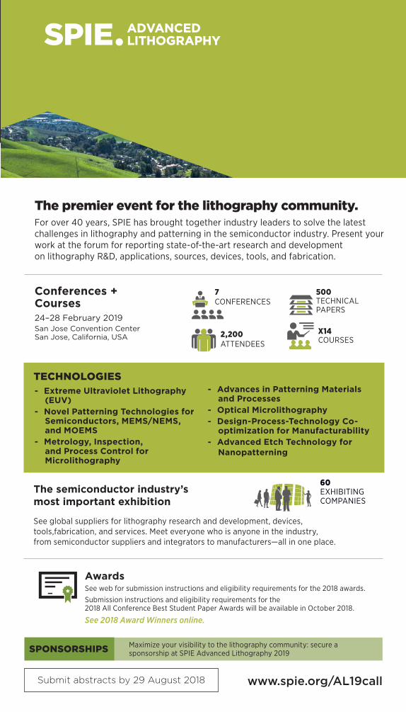
The semiconductor industry’s most important exhibition
See global suppliers for lithography research and development, devices, tools,fabrication, and services. Meet everyone who is anyone in the industry, from semiconductor suppliers and integrators to manufacturers—all in one place.
Conferences and Courses 24–28 February 2019
Exhibition 26–27 February 2019
San Jose Convention Center San Jose, California, USA
The premier event for the lithography community.For over 40 years, SPIE has brought together industry leaders to solve the latest challenges in lithography and patterning in the semiconductor industry. Present your work at the forum for reporting state-of-the-art research and development on lithography R&D, applications, sources, devices, tools, and fabrication.
www.spie.org/AL19callSubmit abstracts by 29 August 2018
- Extreme Ultraviolet Lithography (EUV)
- Novel Patterning Technologies for Semiconductors, MEMS/NEMS, and MOEMS
- Metrology, Inspection, and Process Control for Microlithography
AwardsSee web for submission instructions and eligibility requirements for the 2018 awards.
Submission instructions and eligibility requirements for the 2018 All Conference Best Student Paper Awards will be available in October 2018.
See 2018 Award Winners online.
Maximize your visibility to the lithography community: secure a sponsorship at SPIE Advanced Lithography 2019
TECHNOLOGIES
2,200 ATTENDEES
500 TECHNICAL PAPERS
X14 COURSES
Conferences + Courses 24–28 February 2019San Jose Convention Center San Jose, California, USA
7 CONFERENCES
- Advances in Patterning Materials and Processes
- Optical Microlithography - Design-Process-Technology Co-
optimization for Manufacturability - Advanced Etch Technology for
Nanopatterning
SPONSORSHIPS

Non-
Profi
t Org
.U.
S. P
osta
ge
Paid
SPIE
P.O
. Box
10
Belli
ngha
m, W
A 98
227-
0010
USA
P.O
. Box
10
Belli
ngha
m, W
A 98
227-
0010
USA
CA
LL F
OR
PAP
ER
S
2019
ww
w.s
pie
.org
/AL1
9ca
ll
Shar
e yo
ur r
esea
rch
at t
he s
emic
ond
ucto
r in
dus
try’
s m
ost
imp
orta
nt li
thog
rap
hy e
vent
of t
he y
ear.
24–2
8 Fe
bru
ary
2019
San
Jo
se C
onv
enti
on
Cen
ter
San
Jo
se, C
alifo
rnia
Ad
vanc
ed L
itho
gra
phy
Su
bm
it a
bst
ract
s b
y 29
Au
gu
st 2
018