advances in natural and applied sciences - … · a 50v single input dc buck converter with a power...
TRANSCRIPT

Advances In Natural And Applied Sciences, 9(8) July 2015, Pages: 58-69
AENSI JOURNALS
Advances in Natural and Applied Sciences
ISSN:1995-0772 EISSN: 1998-1090
Journal home page: www.aensiweb.com/ANAS
Corresponding Author: Sasi.G, Department of Electronics and Communication Engineering, Fatima Michael College of
Engineering and Technology, Senkottai Village, Madurai to Sivagangai main road ,Madurai -625
020, Tamilnadu, India.
Mobile No: (0)8300036870. E-mail: [email protected]
FPGA based Switching Noise reduction technique for Multiple Input DC to DC
Converter using Sigma Delta Modulation
1Sasi.G and
2Rajamani.V
1Department of Electronics and Communication Engineering, Fatima Michael College of Engineering and Technology, Senkottai Village,
Madurai to Sivagangai main road, Madurai -625 020, Tamilnadu, India. 2Department of Electronics and Communication Engineering, Veltech Multitech Dr.Rangarajan Dr.Sakunthala Engg College, Chennai -
600062,Tamilnadu India.
A R T I C L E I N F O A B S T R A C T
Article history:
Received 1 June 2015
Accepted 28 June 2015
Available online 22 July 2015
Keywords:
DC–DC power converters,
Electromagnetic Interference, Field
programmable gate arrays, Sigma -
delta modulation, Switching loss.
This paper investigates about the simultaneous switching noise (SSN) reduction in
multiple input DC to DC Buck Boost converters using a technique called Sigma Delta
Modulation (SDM).For a high speed digital system design, the signal integrity issue is
very significant, when multiple switches toggle simultaneously thereby stimulating a
voltage drop in the system. This increases the ground voltage within the device relative
to the system ground. This change of ground voltage produces the noise called SSN or
ground bounce resulting in signal degradation and computation error in digital circuits.
The influence of SSN, even for a single input system, is noticeable and results in loss of
signal quality. On the other hand, if we design for a multiple input, the impact is more
which needs to be addressed. The main cause of this noise is the presence of
inductance and this parasitic inductance effect is reduced by means of a suitable PWM
technique. By using SDM, the harmonics generated around the switching frequency
and the loading effect is minimized for the multiple input converters. This approach
reduces the switching noise by the factor of 0.02dB/decade.
© 2015 AENSI Publisher All rights reserved.
To Cite This Article: Sasi.G and Rajamani.V., FPGA based Switching Noise reduction technique for Multiple Input DC to DC Converter
using Sigma Delta Modulation. Adv. in Nat. Appl. Sci., 9(8): 58-69, 2015
INTRODUCTION
In the present scenario, the impact of renewable
energy sources is more and hence the necessity of DC
to DC converters is also very important. The
converters which are using these multiple renewable
sources encounter certain issues. The three main
issues in converters are switching losses,
electromagnetic interference (EMI) and harmonics.
Many control strategies are available to reduce the
EMI produced by the inductor during switching, but
the spikes are not properly addressed in the existing
technique. The abrupt change in voltage and current
variation due to the action of inductor lead to more
switching noises and needs to be reduced in order to
increase the efficiency. The quality of the input DC
signal also determines the impact of EMI in the
switching converters. The conventional sinusoidal
pulse width modulation (SPWM) uses constant
switching frequency thereby the power spectrum of
harmonics is strengthened near the switching
frequency.
These harmonics spikes result in EMI, switching
losses of MOSFETs and mechanical vibration. A
method called Random PWM (RPWM) is used to
spread the switching frequency by randomly varying
the frequency and duty ratio, but it is somewhat
complex to generate the random switching
phenomenon. In order to overcome these issues, an
alternate method called Sigma Delta Modulation
(SDM) is proposed in this paper. The harmonics
produced near the switching frequency is minimized
by Sigma Delta Modulation technique. SDM has high
resolution and is very simple both in hardware and
software. It produces switching pulses without any
additional ON/OFF computation thereby the
complexity gets reduced. The switching pulses are
randomly changed with constant frequency. The
generated switching pulses are frequency division
multiplexed in order to control multiple input DC to
DC buck boost converter. The factors affecting the
Simultaneous Switching Noise (SSN) are the rate of
change of voltage dv/dt and rate of change of current
di/dt. The dv/dt creates leakage current because of
capacitor and di/dt creates voltage because of the
presence of inductor in the converter and the multiple
switches used in the input of converters. We need to
address multiple input converters to reduce the
switching loss, to increase the efficiency and to
reduce the cost instead of single input converters. In
most of the cases, pulse width modulation techniques
are used in power converter circuits to reduce EMI,

59 Sasi.G and Rajamani.V,2015
Advances in Natural and Applied Sciences, 9(8) July 2015, Pages: 58-69
but the limitations of this technique are that the
spectrum accumulated near the switching frequency
and the additional harmonics are not reduced further.
Even numbers of techniques are used to reduce
this effect but the current stress and the EMI is not
reduced considerably. Some other method called
RPWM is used to spread the signals. The difficulty in
this technique is that the selection of random number
and the duty cycle is limited. Space dither SDM
(SDSDM) and time dither SDM (TDSDM) are used
to reduce these harmonics. The combined SDSDM is
applied to reduce the harmonics by spreading concept
and standard deviation of the sampling process is
calculated. The experimental set up is considered for
a 50v single input DC buck converter with a power
100W and frequency 25kHz (Seo-Hyeong Kim, et
al., 2009). A boost Dc to Dc converter is designed by
using delta sigma modulator and dither technique to
switch on duty reference signal in two stages. By
doing this approach, the maximum noise amplitude is
minimized (Atsushi Hirota, et al., 2011).
A DC to DC converter by delta sigma modulator
by considering the order, oversampling ratio and
input voltage was investigated. Spurious performance
and the efficiency are described. By increasing the
oversampling ratio, the noise is reduced. The
simulation result shows the buck converter with
second order system having input voltage greater
than 0.5v,OSR=64 produces the duty cycle greater
than 75% and input voltage 0.3v,OSR less than 32
produces the duty cycle 65% (Kamala Hariharan, et
al., 2009). A DC to DC buck converter is designed
for a 0.35µm CMOS process by sigma delta
modulator to improve the efficiency and to reduce
noise by taking dead time controller ,Gate width
controller and DCM controller and the efficiency is
achieved to 93% with 30dB harmonic spike
reduction. To reduce the low frequency noise, a
second order SDM is presented (Cai Shujiang, et al.,
2011). The noise present in the power supply, SMPS
is eliminated by sigma delta modulator. The rms
noise power is 75.85 mW. A multibit approach is
applied at quantizer level to reduce the noise spikes
and the results show the rms noise power for 2 bit
controller is 3.75mW and for a 4 bit controller is 0.24
mW. Performance comparison is done for a normal
PWM with 1bit,2 bit and 4 bit SD controller by using
the concept of fixed period and variable frequency
controller. This method is best suited for multibit
scheme at quantizer level conversion (Steven, K.,
Dunlap and Terri S. Fiez, 2004).
A multiple input DC to DC converter is designed
and the effective duty ratio is the integer function of
common duty ratio. Additionally, a proportional
integral (PI) controller is used to regulate this MIC. It
multiplexes the output of various sources into a
common dc buses and frequency division is used.
Experimental results show the switching operation
for open loop and closed loop and stability is
achieved in only one circuit. This method is extended
for digital implementation also (Chimaobi, N., et al.,
2012). Multiple techniques to reduce EMI in DC to
DC converter are discussed like spread spectrum
,normal sine PWM,bifurcation and chaotic PWM
techniques and the performance comparison is done
and simulation is carried out by using MATLAB and
the results on power spectrum are also described. The
power spectra for chaotic spreading and random
PWM techniques are -25 dB/Hz and -23.8-24.4
dB/Hz respectively and it is concluded that among
the various other methods addressed in this paper
these two methods give the best result to reduce the
EMI (Laxman Solankee, et al., 2012).
A DC to DC buck converter is designed and
implemented in the field programmable gate
arrays(FPGA). This enables the high speed dynamic
response and better programming flexibility without
adding more passive components. The transition from
linear to nonlinear is easily achieved at the switching
frequency 100KHz.The PWM controller and the
ADC are implemented in FPGA and the algorithm is
flexible and written in VHDL (Micro Milanovic, et
al., 2005). A multiple input converter with sharing
single secondary windings for single primary
windings corresponding to multiple inputs. Due to its
construction the circuit is simple and easy to
manufacture (Qin Wang, et al., 2011). Some set of
rules are proposed for MIC by decomposing the
converters into basic cells and two families are
generated. One family of MIC all inputs can power
and load simultaneously or individually. In the
second family one source is allowed to transfer
energy to load at a time. Based on the connection
rules a synthesis of MIC has been presented (Yan Li,
et al., 2010).
Multiple input converters have cost effective and
flexible ways to connect more sources and feasible
topologies are designed to expand single input
converter into multiple input converter. Four rules are
formed to identify MIC topology, and six topologies
are designed and their behavior is verified with the
simulations (Alexis Kwasinski, 2009). The static and
the dynamic characteristics are analyzed for the
MIC‟s and the purpose is to realize zero emission
power generation system. A two input buck boost DC
to DC converter is taken as prototype model to
control the operation and three modes are defined.
Mode I is tested under light load condition, in mode
II the output voltage is regulated by optimum power
point and in mode III the output power is zero .In all
the modes, the input source is considered as solar cell
(Hirofumi Matsuo, et al., 2004). A multiple input DC
to DC converter is designed by using a fixed
frequency switching technique for a common load
and low part count. It describes the converter
operation for both CCM and DCM and it does not
address about the isolation, duty cycle limits and
power sharing issues (Bryan, G., Dobbs and Patrick

60 Sasi.G and Rajamani.V,2015
Advances in Natural and Applied Sciences, 9(8) July 2015, Pages: 58-69
L. Chapman, 2003). Another literature for single
input multiple output converter was addressed in
which the outputs are at multiple voltage levels which
can be used to drive different applications and
produces high power conversion efficiency. A
prototype SIMO converter with coupled inductor was
designed with one power switch and maximum
efficiency exceeds 95% and conversion efficiency of
91% is achieved. But this system is not suited for dc-
ac multilevel inverters (Rong-Jong Wai and Kun-
Huai Jheng, 2013).
A CT sigma delta modulator for extended range
is described at ADC level and a third order ΔΣ
modulator was designed. A low power multichannel
applications had been considered for this analysis and
the modulation was carried over ADC during
conversion process. A comparison was performed
with respect to different test algorithms and shows
the importance of non idealities in terms of number
of functions (Julian Garcia, Saul Rodriguez and Ana
Rusu, 2013). The dynamic characteristics of multi
input multi output(MIMO) converter topology was
described for both CCM and DCM mode. Power
budgeting was established between the input sources.
It uses one inductor thereby the circuit complexity
and the cost got reduced and it is capable of
performing Buck and Boost mode operation. Three
inputs and two outputs are considered for this DC to
DC converter (Hamid Behjati and Ali Davoudi,
2013).
By considering quantizer levels and coefficients
of noise system function, a sigma delta modulator
was designed for multibit applications. This does not
use any converters but employs SDM at quantization
levels and also the stability of the modulators is
analyzed. Simulation was done by using MATLAB
and a comparison was performed for three levels and
five level quantizer for different order (Jaswinder
Lota, et al., 2014). A digital controller was designed
for a buck converter at high switching frequency by
means of predictive control technique. It calculates
current and voltage variation and the simulations are
carried out by using MATLAB.The output power for
vertex II FPGA is calculated as 450-682mW and the
performance is analyzed by closed loop (Bo Li, et al.,
2012).
A time sharing multiple inputs converter was
designed in which the switching noise can be reduced
by active clamping method. A soft switching
technique was employed to isolate the TS-MIC and
various components stress was calculated. The
efficiency of active clamping with BSS type III is
higher than with BSS type IV and snubber BSS type
III. The switching loss is also reduced for active
clamping with BSS type III (Sheng-Yang Yu and
Alexis Kwasinski, 2013). A low complexity discrete
time delta sigma modulator was designed and the
chips SNR is 74.32dB and distortion ratio 81dB is
achieved .It consumes 94mW power from 1volt
supply. It results wide bandwidth and high dynamic
range. Thus this modulator was designed at analog to
digital conversion stage and the active area is also
calculated (Su-Hao Wu and Jieh-Tsorng Wu, 2013).
This paper proposes a multiple input DC to DC
Buck Boost converter with a single control strategy
by SDM technique. The paper is organized as
follows. Chapter2gives the proposed work. The
proposed multiple input DC to DC converter with
SDM is addressed in chapter3. Results and
discussion are described in chapter4 and finally
conclusion is addressed in chapter5.
2. Proposed work:
Fig. 1: Proposed block diagram
Fig1 shows the block diagram of the proposed
work. A DC to DC buck boost converter is designed
and this converter can have multiple inputs. Here
three inputs are considered for our analysis. SDM is
provided in the feedback path of the system where a
constant frequency pulses are generated and these
pulses are divided into many switching pulses by
Time Sharing Algorithm (TSA).Here each cycle is
split into three in order to control three inputs of a
converter. The detailed functionalities of SDM and
TSA are described in the successive sections. The
switching pulses at the output of SDM are given to
the three inputs of the converter so that the converter
produces less EMI, harmonics and switching losses

61 Sasi.G and Rajamani.V,2015
Advances in Natural and Applied Sciences, 9(8) July 2015, Pages: 58-69
near the switching frequency. The entire system is in
a closed loop so that the efficiency of the converter is
improved. The quality of the DC inputs applied at the
input of the converter is also increased. The switches
used at the inputs produce switching pulses in a short
period thereby the switching losses are to be
concentrated.
2.1. Sigma Delta Modulation:
Fig. 2: Block diagram of Sigma Delta Modulation
A first order Sigma Delta Modulation (Atsushi
Hirota, et al., 2011) for a power converter circuit is
depicted in Fig2.The analog input voltage is given to
ADC at the bottom of the circuit in Fig2 to produce
digital output and this is given to delay in producing
integrated signal. This signal is given to 1 bit
quantizer to produce sum signal in digital form. The
number of section is our choice with respect to the
order of the system.
)}1()({)1()( nenenxny (1)
Where )(nx is the input signal, )(ne is the
quantization error signal and )(ny is the output
signal.
)(ny =+1 if )(nx ≥ Vref - 1 if )(nx < Vref (2)
Fig.3 Discrete model of SDM
Fig3 shows the simplified discrete time model of
SDM. It also gives the connection diagram of input
and output in z domain along with the noise function
N (z).The transfer function of noise function is
derived below.
By taking Z transform of “(1)”
Y (z) =X (z) z-1
+ E (z) (1-z-1
) (3)
This y (n) is given to the input of a switch. By
using this model, we can define two transfer
functions. One is with respect to signal and another
one is with respect to noise. That is (Seo-Hyeong
Kim, et al., 2009)
Transfer function of signal,
)(
)()(
zX
zYzH sig = z
-1 (4)
Transfer function of noise,
)(
)()(
zE
zYzHnoise = 1-z
-1 (5)
In order to find out the frequency response of the
system, put z=ejωTs
,where Ts =1/fs is the sampling
period. Substitute z=ejωTs
in “(4)”, we get
{ )(zH sig } at z=ejωTs
= e-jωTs
By Euler‟s rule, the above equation can be
written as
{ )(zH sig } = cos ωTs-jsin ωTs
The magnitude response is given by
)( zsigH = 1 (6)
Similarly “(5)” can be simplified as
{)(
)()(
zE
zYzHnoise } at z=e
jωTs = 1-z
-1 = 1-e
-jωTs
The above equation can be rearranged as
{ )(zH noise } at z=ejωTs
= ejωTs/2
e-jωTs/2
- e-jωTs/2
e-
jωTs/2
= e-jωTs/2
[ejωTs/2
- e-jωTs/2
]
By Euler‟s rule
= e-jωTs/2
2 Sin ωTs/2
Or

62 Sasi.G and Rajamani.V,2015
Advances in Natural and Applied Sciences, 9(8) July 2015, Pages: 58-69
= e-jωTs/2
2Sin 2πf/2fs
= e-jωTs/2
2 Sin πf/fs
The magnitude response is given by
)( znoiseH = 2
sf
fSin
(7)
2.2. Time Sharing Algorithm:
The proposed technique is to generate an N
number of switching frequency from Common
Switching Function (CSF) with a higher switching
frequency. This can be achieved by Time Sharing
algorithm by using JK flip-flop in toggle mode and
logic gates. The number of flip-flop required to
generate the switching pulses is based on
N = 2n (8)
Where „n‟ is the number of flip flop and „N‟ is
the number of switching frequencies. In order to
simplify the circuit, the number of inputs are taken as
three. Here we have considered 2 flip-flops.So that in
total we can generate up to 4 switching pulses. Out of
4 switching pulses, three pulses are taken into
consideration for our work and the 4th
output is
reserved for extending the inputs in future.
3,4 MiNj (9)
Where N is the total number of j switching
pulses generated by time sharing concept and M is
the total number of i inputs of the converter.
Fig. 4: Switching technique by time sharing algorithm
In Fig.4, two JK flip-flops are used with two
stages in toggle mode to generate 4 pulses. In the first
stage, the single frequency is divided into two time
slots and in the second stage again this two time slots
are divided into four time slots. In a similar fashion,
we can generate any number of pulses by adding the
stages as per “(8)”.Among the possible outputs „N‟,
only required number (M) which is equal to the
number of inputs is taken and the share factor is
given by (Chimaobi, N., et al., 2012)
N
M (10)
which is always less than or equal to 1.For our
case 4
3 ≤ 1.The effective duty cycle is the
multiple of share factor of CSF and the fundamental
frequency is given by
N
ff CSF (11)
effD DCSF (12)
2.3. Correlation between sampling period and
switching frequency:
To analyze the behavior of harmonics in SDM,
the variation of switching periods is tested. As per the
Nyquist theorem, if the sampling frequency is larger
than the input maximum frequency, then the
frequency ratio of SDM with SPWM will be
calculated if fs is equal to the carrier frequency of
SPWM. The relationship is plotted for both DC input
and AC input. For a DC input (Seo-Hyeong Kim, et
al., 2009),
mR2
1
2
1 (13)
Where m is the modulation index
For a AC input,
mR
1
2
1 (14)
To analyze the change in output switching
period, the switching number per switching cycle is
calculated. From “(13)”
The possible value of sampling number is given
by

63 Sasi.G and Rajamani.V,2015
Advances in Natural and Applied Sciences, 9(8) July 2015, Pages: 58-69
xegerns
1
2int (15)
where x is the input at the starting point of
switching cycle. If the input is zero, then the
sampling number ns will be 2.If the input is larger
than the sampling number will also be higher and the
value will be increasing with increase in input value
(x).
3. Proposed Multiple Input Buck Boost Converter
with SDM:
Fig. 5: Multiple Input converter with SDM
Fig.5 illustrates SDM scheme for three inputs
DC to DC converter by using TSA. Due to the
multiple switching, the converter may experience
excess harmonics and switching noise which will
reduce the efficiency of the converter. To eliminate
this issue, an SDM discussed earlier is introduced
which reduces the issue related to harmonics and
switching noises. This switching scheme further
utilizes the Time Sharing Algorithm which a single
PWM cycle is divided into equal periods according
to the number of inputs. The split signal is given to
the gate control of switching devices. To operate on a
voltage control mode, the output of converter is taken
as the feedback through an ADC to the PID
controller which provides necessary control signal to
maintain a set point voltage and tracked voltage. This
operation is continued until the set point voltage is
achieved. Here a first order SDM section is taken
into consideration. The SDM uses an integrator and
quantizer in the feedback path and makes the
converter circuit in a closed loop manner. The output
of quantizer is +1 or -1 and the difference between
input and quantizer output results the quantization
noise.
The output is feedback to the input of ADC
where it is converted into digital form by comparing
this with the reference voltage. This digital output is
given to the input of PID controller where the digital
implementation of PID controller is performed to
produce the output.
We know that the analog PID controller equation
is given by
t
DI
tedt
dTdtte
TteKtu
0
)()(1
)()( (16)
Where K, TI, TD are adjustable parameters of
PID controller and e (t) is the error signal. Equation
(16) can be rearranged as in digital representation of
PID controller
)2(
)1(2)(
)()}1(
)({)1()(
ke
keke
T
K
keTKke
keKkuku
S
D
SI
p
(17)
Where k is the sample number
Ts is the sampling period
KP is the gain of the proportional control
KI is the gain of the integral control
KD is the gain of the derivative control
U (k) is the output of controller
Equation (17) gives the output of digital PID
controller and this output is given to the input of
SDM.
RESULTS AND DISCUSSION

64 Sasi.G and Rajamani.V,2015
Advances in Natural and Applied Sciences, 9(8) July 2015, Pages: 58-69
Fig. 6(a): Simulation result of Input & output Voltage of Buck Boost converter for V1=V2=V3=5V
Fig. 6(b): Experimental result of Input & output Voltage of Buck Boost converter for V1=V2=V3=5V
Fig.6(a) shows the simulation result and
Fig.6(b) shows the experimental result of input and
output voltages of Buck Boost converter for equal
input voltages. Here the three inputs V1, V2 and V3
are set to 5V and the corresponding output voltage
Vout is 15 V. That is, this converter acts as a Boost
converter for the designed output 15 V.
Fig.7(a): Simulation result of Input & output Voltage of Buck Boost converter for V1=0,V2=5,V3=10V

65 Sasi.G and Rajamani.V,2015
Advances in Natural and Applied Sciences, 9(8) July 2015, Pages: 58-69
Fig. 7(b): Experimental result of Input & output Voltage of Buck Boost converter for V1=0,V2=5,V3=10V
Fig.7(a) shows the simulation result and Fig.7(b)
shows the experimental result of input and output
voltages of Buck Boost converter for unequal inputs.
The three inputs are V1=0V, V2=5V and V3= 10 V.
The output voltage is 15 V and so it works as boost
mode.
Fig. 8(a): Simulation result of Input & output Voltage of Buck Boost converter for V1=V2=0,V3=10V
Fig. 8(b): Experimental result of Input & output Voltage of Buck Boost converter for V1=V2=0,V3=10V
The input and the output voltages of simulation
and experimental result are illustrated in Fig.8(a) and
Fig.8(b) respectively. It is clear from the figure that
the three inputs V1 =V2=0V and V3 is 10V and the
output voltage is 15 V. Here also the converter acts
as boost mode.

66 Sasi.G and Rajamani.V,2015
Advances in Natural and Applied Sciences, 9(8) July 2015, Pages: 58-69
Fig. 9(a): Simulation result of Input & output Voltage of Buck Boost converter for V1=5,V2=0,V3=20V
Fig. 9(b): Experimental result of Input & output Voltage of Buck Boost converter for V1=5,V2=0,V3=20V
Fig.9(a) shows the simulation result and Fig.9(b)
shows the experimental result of input and the output
voltages of Buck Boost converter for unequal inputs.
Here V1=5V, V2=0V and V3 is 20 V and the
converter Output is 15 V. The converter acts as both
buck and boost mode.
Fig. 10: FFT of SDM PWM control (a) theoretical (b) practical

67 Sasi.G and Rajamani.V,2015
Advances in Natural and Applied Sciences, 9(8) July 2015, Pages: 58-69
The frequency response of Sigma Delta
Modulated PWM control is shown in Fig.10(a) & (b)
for theoretical and practical response respectively. It
is clear from the plot that the spectrum is spreaded
over the entire frequency range instead of
concentrating near the switching frequency. Thus, the
SDM reduces the switching noise by the factor of
0.02 dB/decade. From Fig.10(a) the noise reduces to
0dB near the 1kHz but in practical response
(Fig10(b)) this noise is decreased to 0.02 dB/decade
and the design is limited to the maximum of
400kHz.Since our inductor is designed upto this
resonant frequency and hence the switching noise is
decreased at this maximum frequency.
Fig. 11: Switching pulses of proposed system
The switching pulses of our proposed system are
illustrated in Fig.11.It is obvious from the graph that
the system requires to initiate the switching pulses is
375µs.That is, the system which is ready to produce
the switching pulses takes 375µs from the initial set
up.
Fig. 12: Output of SDM
Fig.12 depicts the output of SDM in a separate
form. It is clear from the graph that the pulses are not
equal as the operation of sigma delta modulator. It
was observed that the pulse width was not equal and
it follows as per the random variation of SDM
technique in a closed system.
Fig. 13: Experimental set up
68 Sasi.G and Rajamani.V,2015
Advances in Natural and Applied Sciences, 9(8) July 2015, Pages: 58-69
Fig.13 shows the experimental set up of our
proposed system. This consists of three inputs driven
by three MOSFET switches, buck boost DC to DC
converter. The required SDM waveform is generated
by Xilinx FPGA processor and is driven the power
converter to control the output to reduce the SSN.
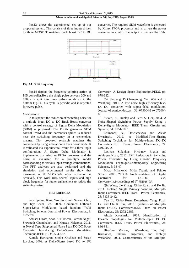
Fig. 14: Split frequecny
Fig.14 depicts the frequency splitting action of
PID controller.Here the single pulse between 200 and
600µs is split into three pulses as shown in the
bottom Fig.14.This cycle is periodic and is repeated
for every pulse.
Conclusions:
In this paper, the reduction of switching noise for
a multiple input DC to DC Buck Boost converter
with a control strategy of Sigma Delta Modulation
(SDM) is proposed. The FPGA generates SDM
control PWM and the harmonics spikes is reduced
near the switching frequency in a tremendous
manner. This proposed research examines the
converters by using simulation in buck boost mode. It
is validated via experimental result for a three input
configuration. A Sigma Delta Modulator is
implemented by using an FPGA processor and the
noise is evaluated for a prototype model
corresponding to various input voltage combinations.
The FFT analyses are also performed and the
simulation and experimental results show that
maximum of 0.02dB/decade noise reduction is
achieved. This work uses several inputs and high
clock frequency for futher enhanement to reduce the
switching noise.
REFERENCES
Seo-Hyeong Kim, Woojin Choi, Sewan Choi,
and Kyo-Beum Lee. 2009. Combined Dithered
Sigma-Delta Modulation based Random PWM
Switching Scheme. Journal of Power Electronics., 9:
667-678.
Atsushi Hirota, Soon-Kurl Kwon, Satoshi Nagai,
Srawouth Chandhaket, and Mutsuo Nakaoka, 2011.
A Novel Type Suppressed Noise Peak DC-DC Boost
Converter Introducing Delta-Sigma Modulation
Technique.IEEE PEDS,.534-537.
Kamala Hariharan, Shoba Krishnan and Susan
Luschas, 2009. A Delta-Sigma based DC to DC
Converter- A Design Space Exploration.PEDS, pp:
678-682.
Cai Shujiang, Pi Changming, Yan Wei and Li
Wenhong, 2011. A low noise high efficiency buck
DC–DC converter with sigma–delta modulation.
Journal of semiconductors., 32: 075004-1 to 075004-
8.
Steven, K., Dunlap and Terri S. Fiez, 2004. A
Noise-Shaped Switching Power Supply Using a
Delta–Sigma Modulator. IEEE Trans. Circuits and
Systems, 51: 1051-1061.
Chimaobi, N., Onwuchekwa and Alexis
Kwasinski, 2012. A Modified-Time-Sharing
Switching Technique for Multiple-Input DC–DC
Converters.:IEEE Trans. Power Electronics., 27:
4492-4502.
Laxman Solankee, Krishnav Bhatia and
Ashfaque Khan, 2012. EMI Reduction in Switching
Power Converter by Using Chaotic Frequency
Modulation Technique.Contemporary Engineering
Sciences, 5: 33-47.
Micro Milanovic, Mitja Truntic and Primoz
Slibar, 2005. “FPGA Implementation of Digital
Controller for DC-DC Buck
Converter.In.Proceedings of 9th
IDEAS‟05.
Qin Wang, Jie Zhang, Xinbo Ruan, and Ke Jin,
2011. Isolated Single Primary Winding Multiple-
Input Converters. IEEE Trans. Power Electronics.,
26: 3435-3442.
Yan Li, Xinbo Ruan, Dongsheng Yang, Fuxin
Liu and Chi K. Tse, 2010. Synthesis of Multiple-
Input DC/DC Converters.IEEE Trans on Power
Electronics., 25: 2372-2385.
Alexis Kwasinski, 2009. Identification of
Feasible Topologies for Multiple-Input DC–DC
Converters. IEEE Trans. Power Electronics., 24:
856-861.
Hirofumi Matsuo, Wenzhong Lin, Fujio
Kurokawa, Tetsuro Shigemizu, and Nobuya
Watanabe, 2004. Characteristics of the Multiple-

69 Sasi.G and Rajamani.V,2015
Advances in Natural and Applied Sciences, 9(8) July 2015, Pages: 58-69
Input DC–DC Converter.IEEE Trans.Industrial
Electronics, 51: 625-631.
Bryan, G., Dobbs and Patrick L. Chapman,
2003. A Multiple-Input DC-DC Converter Topology.
IEEE Power Electronics letters, 1: 6-9.
Rong-Jong Wai and Kun-Huai Jheng, 2013.
“High-Efficiency Single-Input Multiple-Output DC–
DC Converter.:IEEE Trans. Power Electronics, 28:
886-898.
Julian Garcia, Saul Rodriguez and Ana Rusu,
2013. “On Continuous-Time Incremental ΣΔ ADCs
With Extended Range.: IEEE Trans. Instrumentation
and Measurement., 62: 60-70.
Hamid Behjati and Ali Davoudi, 2013. “A
Multiple-Input Multiple-Output DC–DC
Converter.:IEEE Transactions on Industry
Applications., 49: 1464-1479.
Jaswinder Lota, Mohammed Al-Janabi and Izzet
Kale, 2014. Nonlinear Stability Prediction of Multibit
Delta–Sigma Modulators for Sinusoidal Inputs.:IEEE
Trans. Instrumentation and Measurement., 63: 60-70.
Bo Li, Xuefang Lin-Shi Bruno Allard and Jean-
Marie Rétif, 2012. A Digital Dual-State-Variable
Predictive Controller for High Switching Frequency
Buck Converter With Improved Σ-Δ DPWM. IEEE
Trans.Industrial Informatics, 8: 472-481.
Sheng-Yang Yu and Alexis Kwasinski, 2013.
Analysis of Soft-Switching Isolated Time-Sharing
Multiple-Input Converters for DC Distribution
Systems. IEEE Trans.Power Electronics, 28: 1783-
1794.
Su-Hao Wu and Jieh-Tsorng Wu, 2013. A 81-dB
Dynamic Range 16-MHz Bandwidth ΔΣModulator
Using Background Calibration. IEEE Journal of
Solid-State Circuits., 48: 2170-2179.