advancing strained silicon
DESCRIPTION
Advancing Strained Silicon. A O’Neill , S Olsen, University of Newcastle P-E Hellstrom, M Ostling, KTH K Lyutovich, E Kasper, University of Stuttgart. Scope. First investigation of thin VS MOSFETs 10x reduction in virtual substrate thickness Reduced self-heating Reduced growth time - PowerPoint PPT PresentationTRANSCRIPT
Advancing Strained Silicon
A O’Neill, S Olsen, University of NewcastleP-E Hellstrom, M Ostling, KTH
K Lyutovich, E Kasper, University of Stuttgart

Scope
• First investigation of thin VS MOSFETs– 10x reduction in virtual substrate thickness– Reduced self-heating – Reduced growth time– Compare thin with thick VS MOSFET
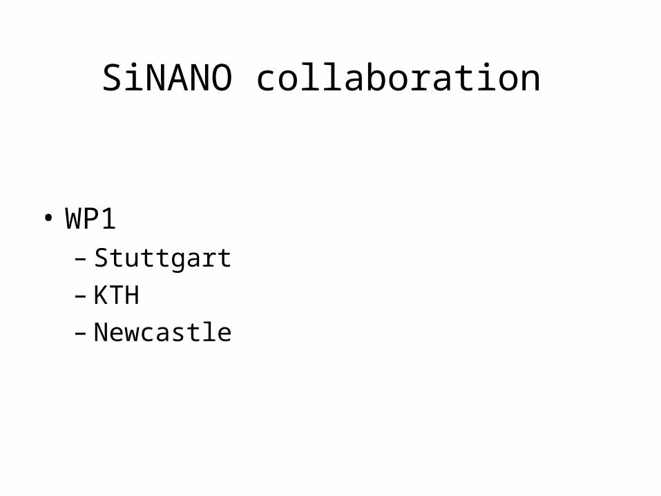
SiNANO collaboration
• WP1– Stuttgart– KTH– Newcastle
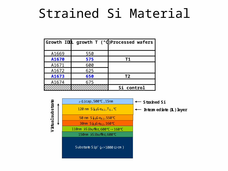
Substrate Si p — (>1000 · ·cm)
150nm i - Si b uffer, 600°C
110nm i - Si b uffer, 600°C 160°C
30nm Si 0.8 Ge 0.2 , 160°C
50 nm Si 0.8 Ge 0.2 , 550°C
120 nm Si0.8Ge0.2, TIL, °C
-Si cap, 500°C, 15nm
Vir
tual
su
bst
rate
Strained Si
Intermediate (IL) layer
Strained Si Material
Growth ID IL growth T (°C) Processed wafers
A1669 550A1670 575 T1A1671 600A1672 625A1673 650 T2A1674 675
Si control
Processing
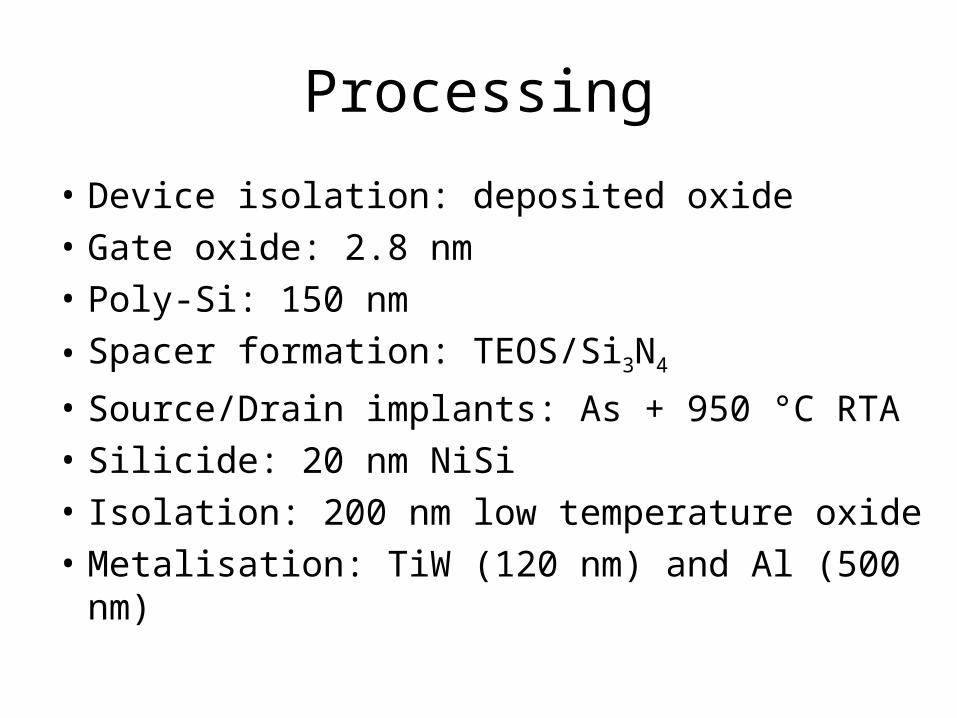
• Device isolation: deposited oxide• Gate oxide: 2.8 nm• Poly-Si: 150 nm
• Spacer formation: TEOS/Si3N4
• Source/Drain implants: As + 950 °C RTA• Silicide: 20 nm NiSi• Isolation: 200 nm low temperature oxide• Metalisation: TiW (120 nm) and Al (500 nm)

nMOSFET
• no cross-hatching or dislocation pile-ups

Wafer yield
T2 T1 Si control
53.4% 89.7% 65.5%
yield not determined by material quality (yield on Si control is only 65%)Lg = 10 m
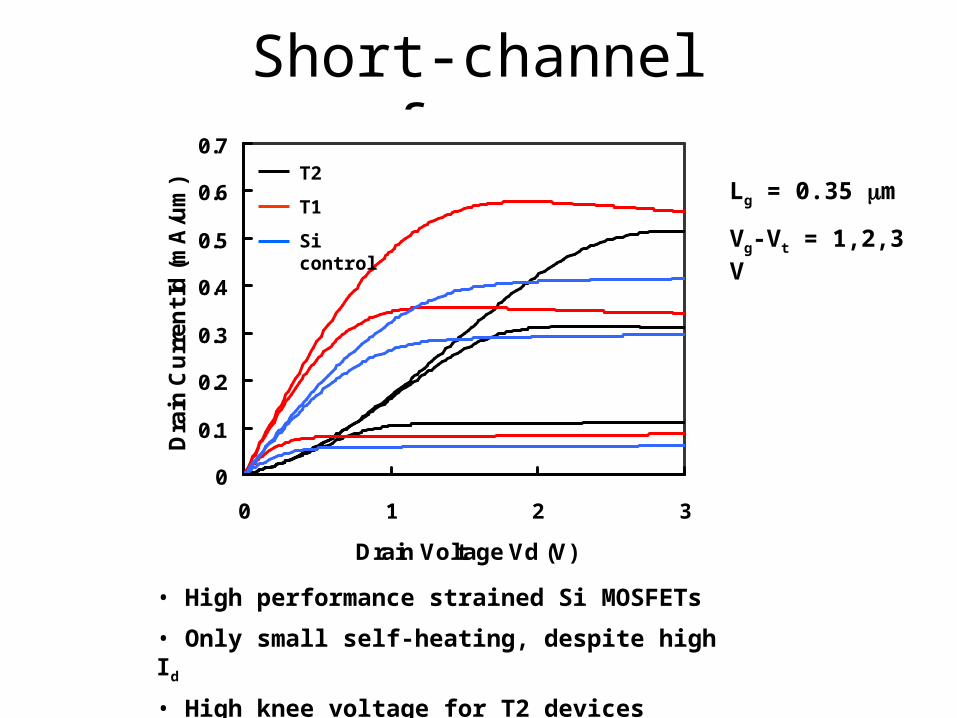
Short-channel performance
• High performance strained Si MOSFETs
• Only small self-heating, despite high Id
• High knee voltage for T2 devices
Lg = 0.35 m
Vg-Vt = 1,2,3 V
0
0.1
0.2
0.3
0.4
0.5
0.6
0.7
0 1 2 3
Drain Voltage Vd (V)
Dra
in C
urr
ent I
d (
mA
/um
) T2
T1
Si control
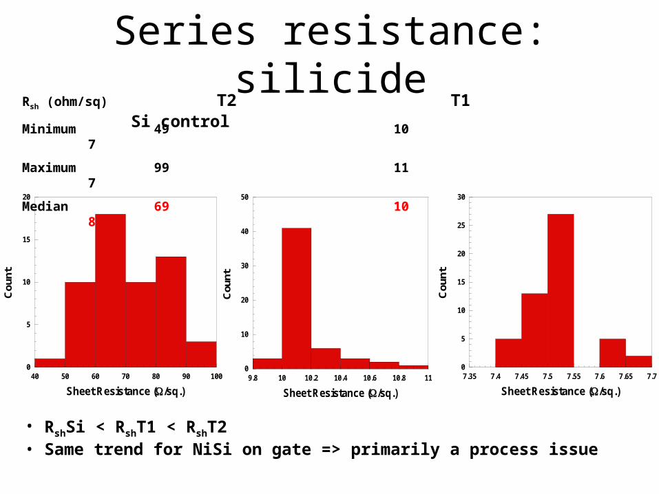
Series resistance: silicide
0
5
10
15
20
40 50 60 70 80 90 100
Cou
nt
Sheet Resistance (/sq.)
0
10
20
30
40
50
9.8 10 10.2 10.4 10.6 10.8 11
Cou
nt
Sheet Resistance (/sq.)
0
5
10
15
20
25
30
7.35 7.4 7.45 7.5 7.55 7.6 7.65 7.7
Cou
nt
Sheet Resistance (/sq.)
• RshSi < RshT1 < RshT2• Same trend for NiSi on gate => primarily a process issue
Rsh (ohm/sq) T2 T1 Si control
Minimum 49 10 7
Maximum 99 11 7
Median 69 10 8
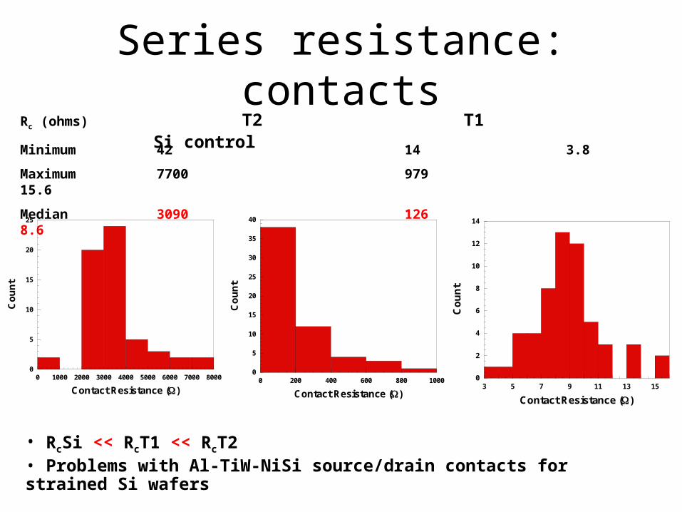
Series resistance: contacts
• RcSi << RcT1 << RcT2• Problems with Al-TiW-NiSi source/drain contacts for strained Si wafers
Rc (ohms) T2 T1 Si control
Minimum 42 14 3.8
Maximum 7700 979 15.6
Median 3090 126 8.6
0
5
10
15
20
25
0 1000 2000 3000 4000 5000 6000 7000 8000
Co
un
t
Contact Resistance ()0
2
4
6
8
10
12
14
3 5 7 9 11 13 15
Co
un
t
Contact Resistance ()
0
5
10
15
20
25
30
35
40
0 200 400 600 800 1000
Contact Resistance ()
Co
un
t
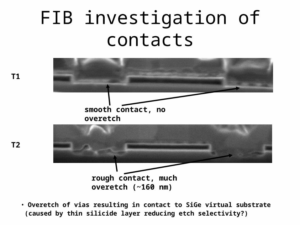
FIB investigation of contacts
smooth contact, no overetch
rough contact, much overetch (~160 nm)
T1
T2
• Overetch of vias resulting in contact to SiGe virtual substrate (caused by thin silicide layer reducing etch selectivity?)
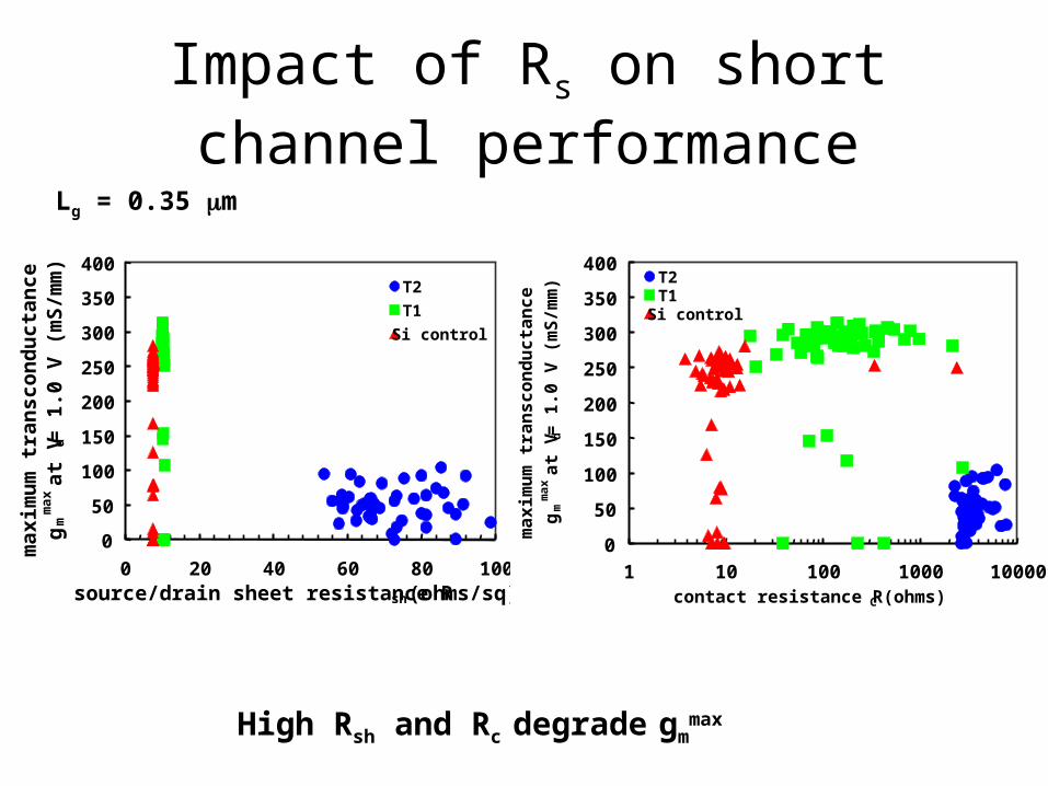
Impact of Rs on short channel performance
Lg = 0.35 m
High Rsh and Rc degrade gmmax
0
50
100
150
200
250
300
350
400
0 20 40 60 80 100source/drain sheet resistance Rsh (ohms/sq)
max
imu
m t
ran
sco
nd
uct
ance
g
mm
ax a
t V
d =
1.0
V (
mS
/mm
)
T2
T1
Si control
0
50
100
150
200
250
300
350
400
1 10 100 1000 10000contact resistance R C (ohms)
ma
xim
um
tra
ns
co
nd
uc
tan
ce
gm
max
at
Vd =
1.0
V (
mS
/mm
)
T2T1Si control

Impact of Rs on long channel performance
Lg = 10 m
Little impact of high Rsh and Rc on long channel performance=> concentrate analysis on large geometry devices
0
5
10
15
20
25
30
0 20 40 60 80 100source/drain sheet resistance Rsh (ohm/sq)
max
imu
m t
ran
sco
nd
uct
ance
g
mm
ax a
t V
d =
1.0
V (
mS
/mm
)
T2T1Si-control
0
5
10
15
20
25
30
1 10 100 1000 10000
contact resistance R c (ohms)
max
imu
m t
ran
sco
nd
uct
ance
gm
max
at
Vd
= 1
.0 V
(m
S/m
m)
T2T1Si-control
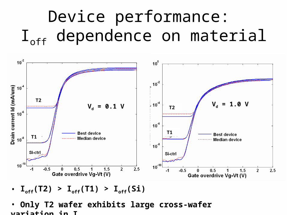
Device performance: Ioff dependence on material
Vd = 0.1 V Vd = 1.0 V
Lg = 10 m
• Ioff(T2) > Ioff(T1) > Ioff(Si)
• Only T2 wafer exhibits large cross-wafer variation in Ioff
T2
T1
T2
T1
Vd = 0.1 V
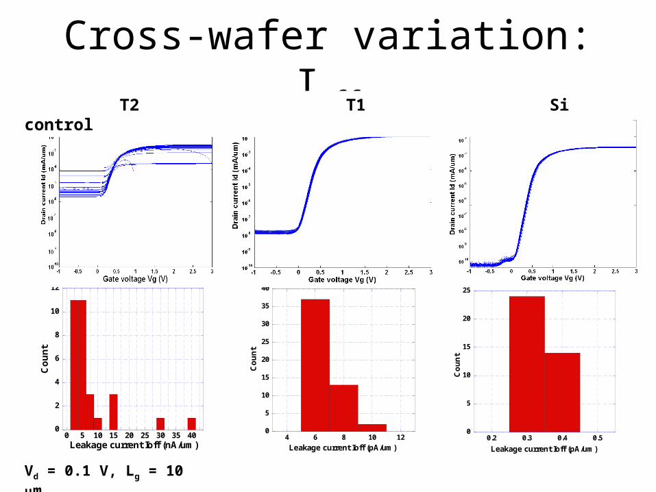
Cross-wafer variation: Ioff
0
2
4
6
8
10
12
0 5 10 15 20 25 30 35 40
Co
un
t
Leakage current Ioff (nA/um)
Vd = 0.1 V, Lg = 10 m
0
5
10
15
20
25
30
35
40
4 6 8 10 12
Co
un
t
Leakage current Ioff (pA/um)
0
5
10
15
20
25
0.2 0.3 0.4 0.5
Co
un
tLeakage current Ioff (pA/um)
T2 T1 Si control
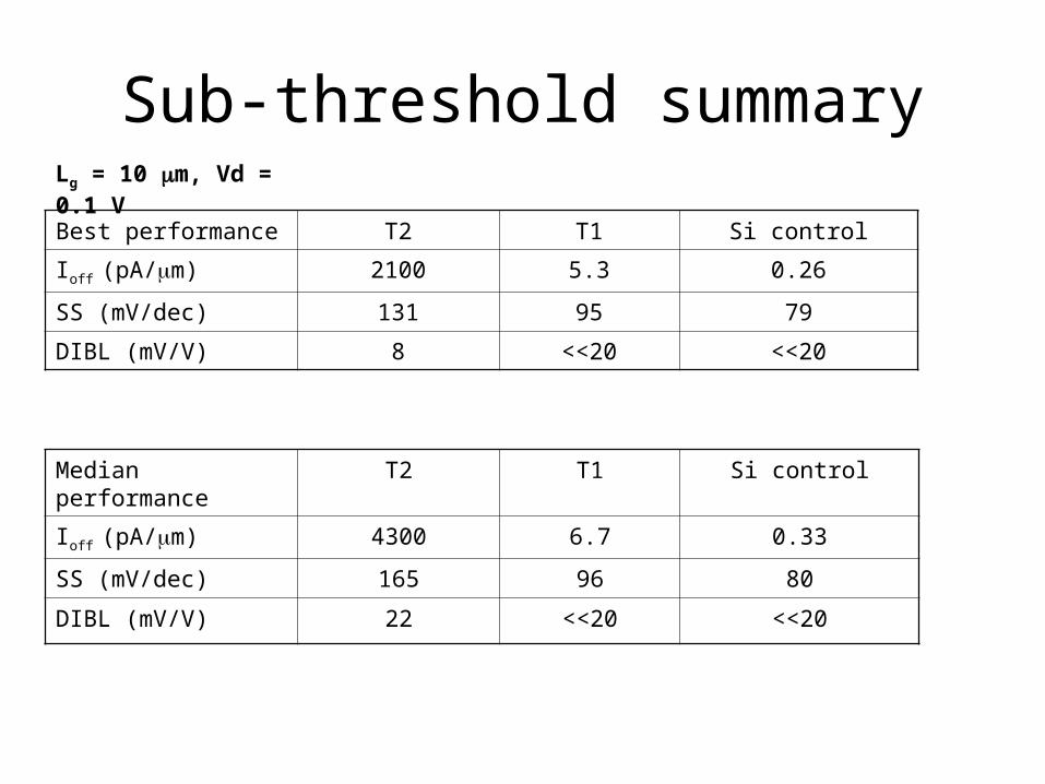
Sub-threshold summary
Best performance T2 T1 Si control
Ioff (pA/m) 2100 5.3 0.26
SS (mV/dec) 131 95 79
DIBL (mV/V) 8 <<20 <<20
Lg = 10 m, Vd = 0.1 V
Median performance T2 T1 Si control
Ioff (pA/m) 4300 6.7 0.33
SS (mV/dec) 165 96 80
DIBL (mV/V) 22 <<20 <<20
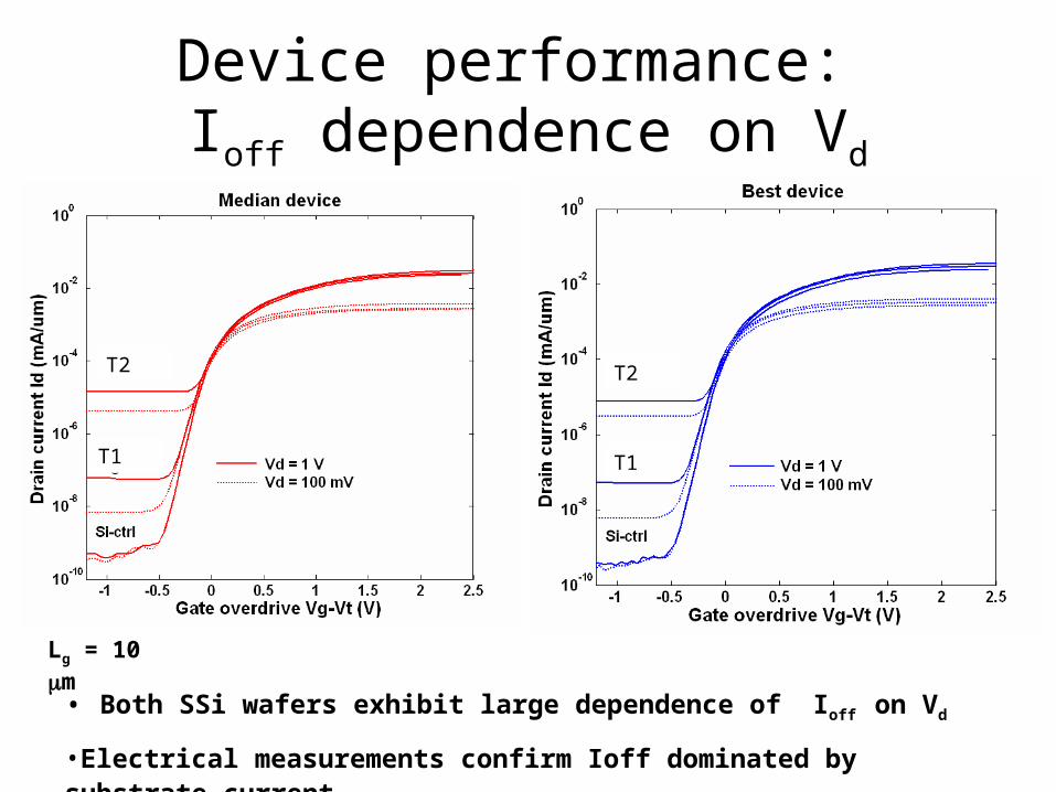
Device performance: Ioff dependence on Vd
• Both SSi wafers exhibit large dependence of Ioff on Vd
•Electrical measurements confirm Ioff dominated by substrate current
Lg = 10 m
T2
T1 T1
T2
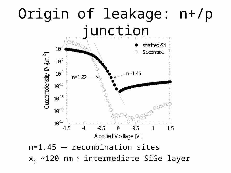
Origin of leakage: n+/p junction
n=1.45 recombination sites
xj ~120 nm intermediate SiGe layer
10-17
10-15
10-13
10-11
10-9
10-7
10-5
-1.5 -1 -0.5 0 0.5 1 1.5
Si controlstrained-Si
Cur
rent
den
sity
[A
/m
2 ]
Applied Voltage [V]
n=1.02n=1.45

Origin of leakage: defects
• Reverse processing on best-performing devices (gate regions)
• Schimmel etch consisting of CrO3/HF
• Increased defect density on material grown at T2
100 m
Etch pit density: 2.2x106 cm-2
100 m
T2 T1
Etch pit density: 9x105 cm-2
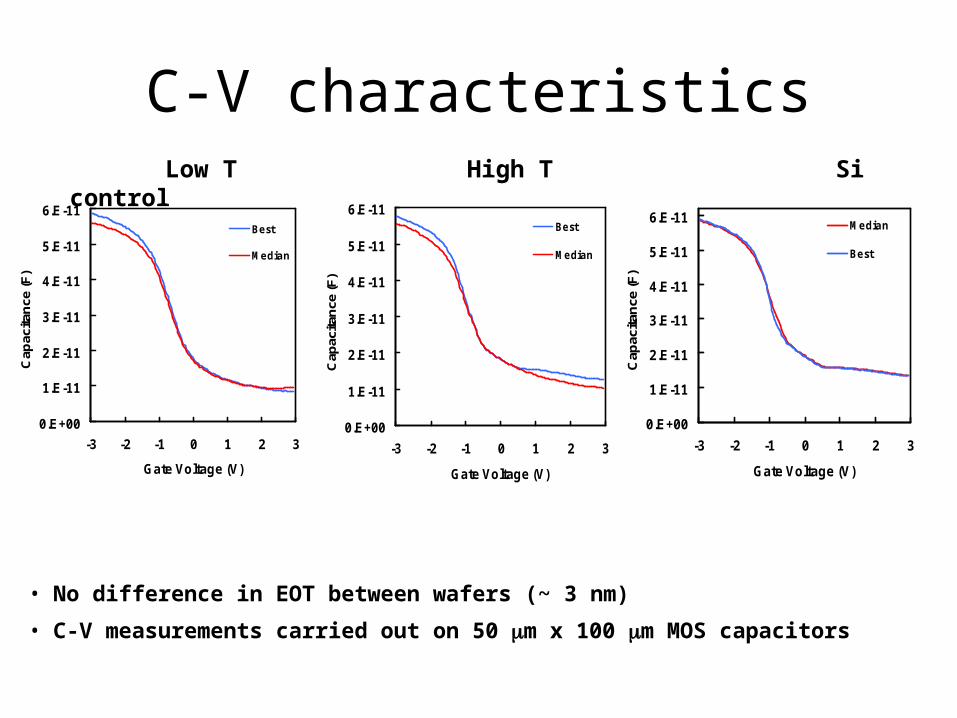
C-V characteristics
0.E+00
1.E-11
2.E-11
3.E-11
4.E-11
5.E-11
6.E-11
-3 -2 -1 0 1 2 3
Gate Voltage (V)
Cap
acita
nce
(F)
Median
Best
0.E+00
1.E-11
2.E-11
3.E-11
4.E-11
5.E-11
6.E-11
-3 -2 -1 0 1 2 3
Gate Voltage (V)
Cap
acita
nce
(F)
Best
Median
0.E+00
1.E-11
2.E-11
3.E-11
4.E-11
5.E-11
6.E-11
-3 -2 -1 0 1 2 3
Gate Voltage (V)
Cap
acita
nce
(F)
Best
Median
Low T High T Si control
• No difference in EOT between wafers (~ 3 nm)
• C-V measurements carried out on 50 m x 100 m MOS capacitors
1.E+11
1.E+12
1.E+13
T1 T2 Si Control
Dit (
cm-2
eV-1
)
Median
Best
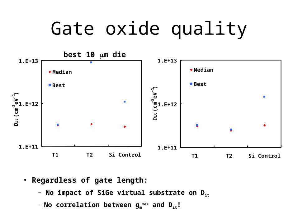
Gate oxide quality
• Regardless of gate length:
– No impact of SiGe virtual substrate on Dit
– No correlation between gm
max and Dit!
best 10 m die best 0.35 m die
1.E+11
1.E+12
1.E+13
T1 T2 Si ControlD
it (
cm-2
eV-1
)
Median
Best
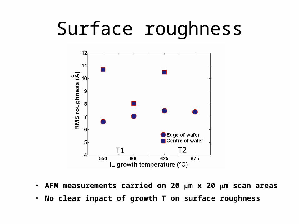
Surface roughness
• AFM measurements carried on 20 m x 20 m scan areas
• No clear impact of growth T on surface roughness
T1 T2
0
5000
1 104
1.5 104
2 104
480 490 500 510 520 530 540
A1674
EdgeMiddleCentre
Inte
nsity
Wavenumber (cm-1)
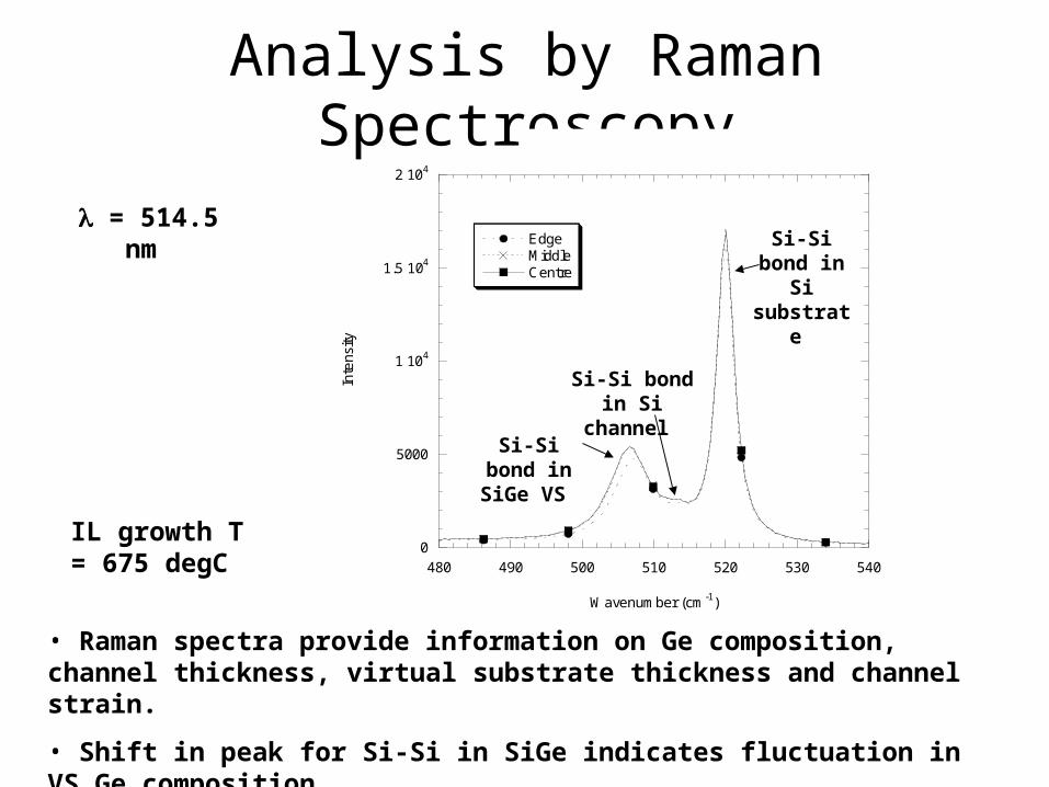
Analysis by Raman Spectroscopy
• Raman spectra provide information on Ge composition, channel thickness, virtual substrate thickness and channel strain.
• Shift in peak for Si-Si in SiGe indicates fluctuation in VS Ge composition
• Spectra may also be influenced by defectivity
= 514.5 nm
IL growth T = 675 degC
Si-Si bond in Si
substrate
Si-Si bond in Si channel
Si-Si bond in SiGe VS
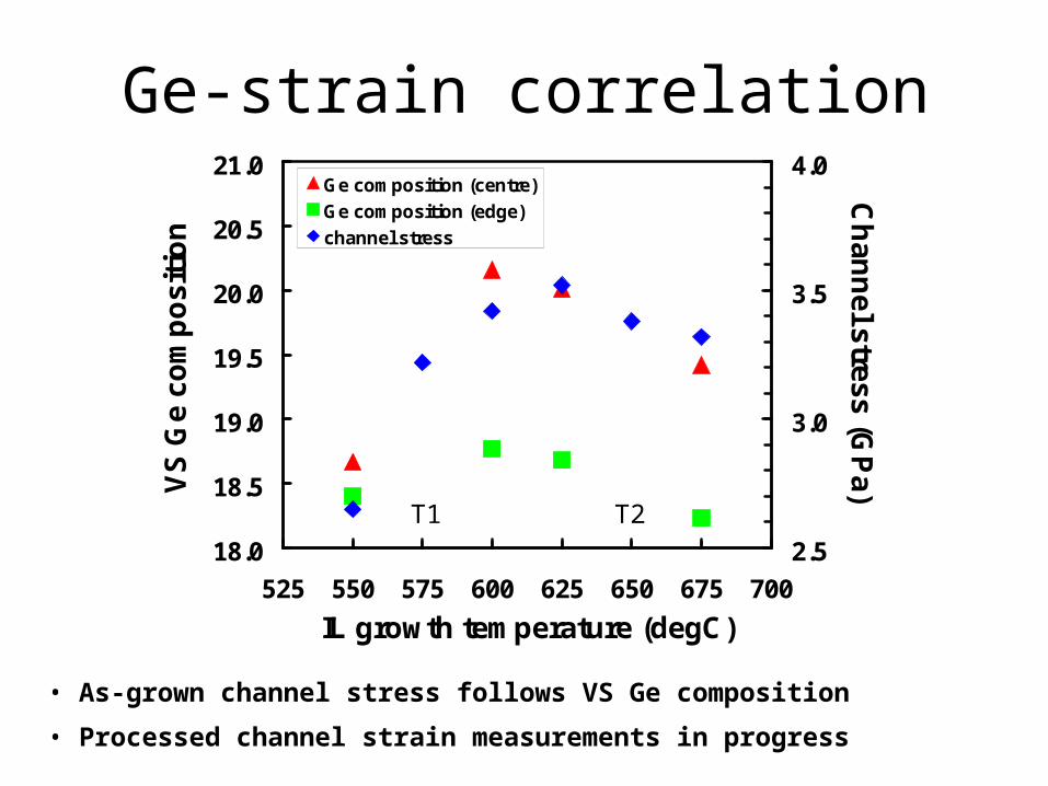
Ge-strain correlation
18.0
18.5
19.0
19.5
20.0
20.5
21.0
525 550 575 600 625 650 675 700
IL growth temperature (degC)
VS
Ge
com
po
sit
ion
2.5
3.0
3.5
4.0C
ha
nn
el stre
ss (GP
a)Ge composition (centre)
Ge composition (edge)
channel stress
• As-grown channel stress follows VS Ge composition
• Processed channel strain measurements in progress
T1 T2

Drain current enhancements
~ Uniform enhancements in Ion with Vd suggest little self-heating
L=W=10um
T1T2
T2T1Si

Mobility enhancement ~ 50%
0
50
100
150
200
250
300
350
400
0.4 0.6 0.8 1 1.2 1.4
strained-SiSi controlUniversal mobility
Eff
ectiv
e E
lect
ron
Mob
ility
[cm
2 /Vs)
Effective Electric Field [MV/cm]
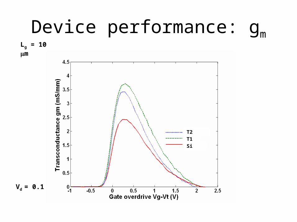
Device performance: gmLg = 10 m
Vd = 0.1 V
T2
T1
Si
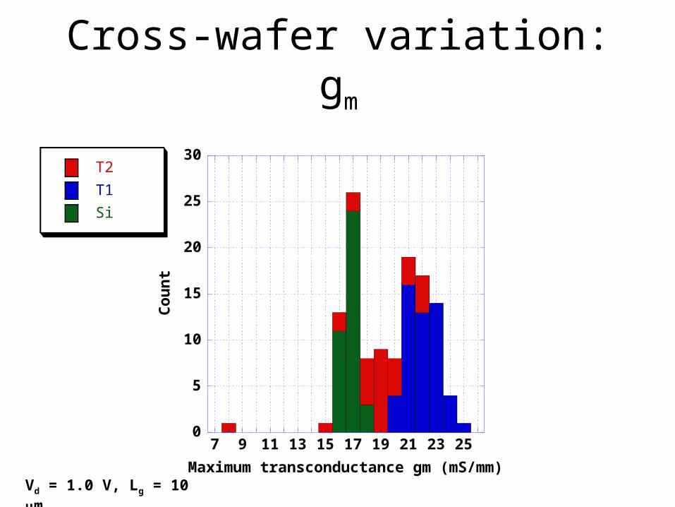
Cross-wafer variation: gm
Vd = 1.0 V, Lg = 10 m
0
5
10
15
20
25
30
7 9 11 13 15 17 19 21 23 25
T2
T1
Si
Co
un
t
Maximum transconductance gm (mS/mm)
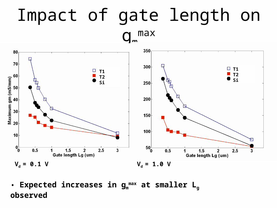
Impact of gate length on gmmax
• Expected increases in gmmax at smaller Lg observed
Vd = 0.1 V Vd = 1.0 V
T1T2Si
T1T2Si
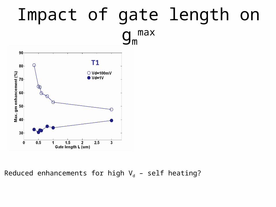
Impact of gate length on gmmax
T1
Reduced enhancements for high Vd – self heating?
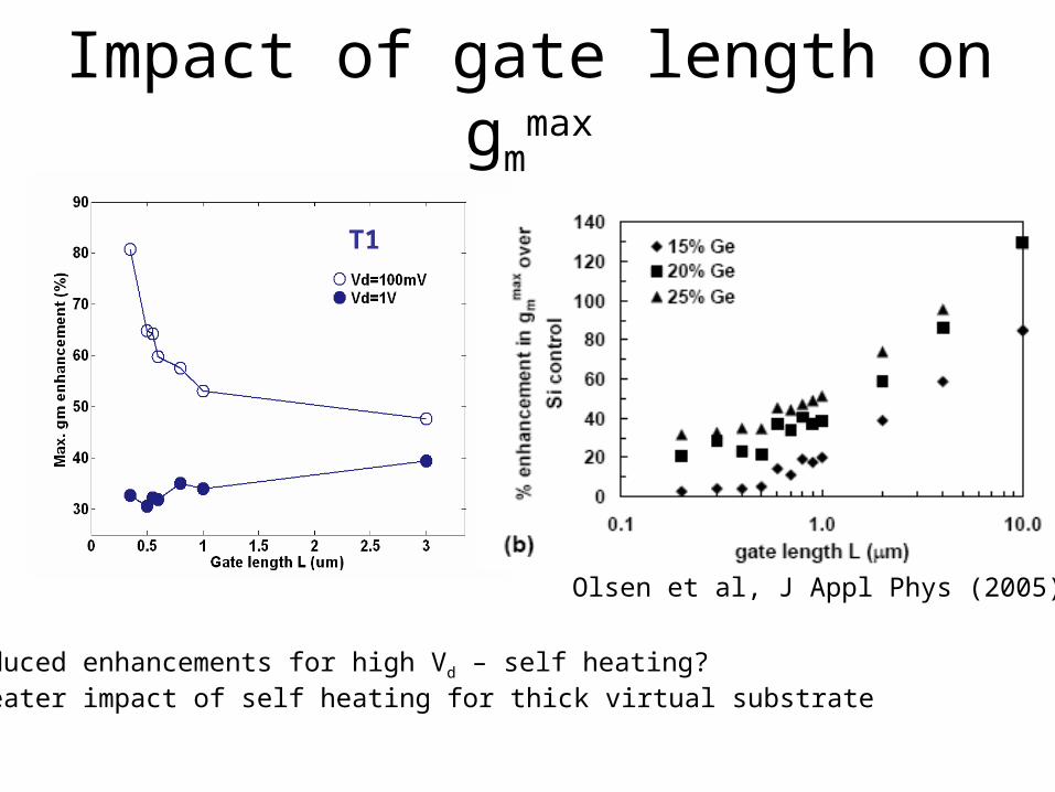
Impact of gate length on gmmax
T1
Olsen et al, J Appl Phys (2005)
Reduced enhancements for high Vd – self heating?Greater impact of self heating for thick virtual substrate
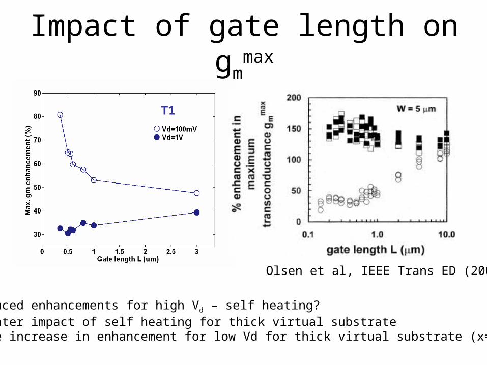
Impact of gate length on gmmax
T1
Olsen et al, IEEE Trans ED (2003)
Reduced enhancements for high Vd – self heating?Greater impact of self heating for thick virtual substrateSame increase in enhancement for low Vd for thick virtual substrate (x=0.15)
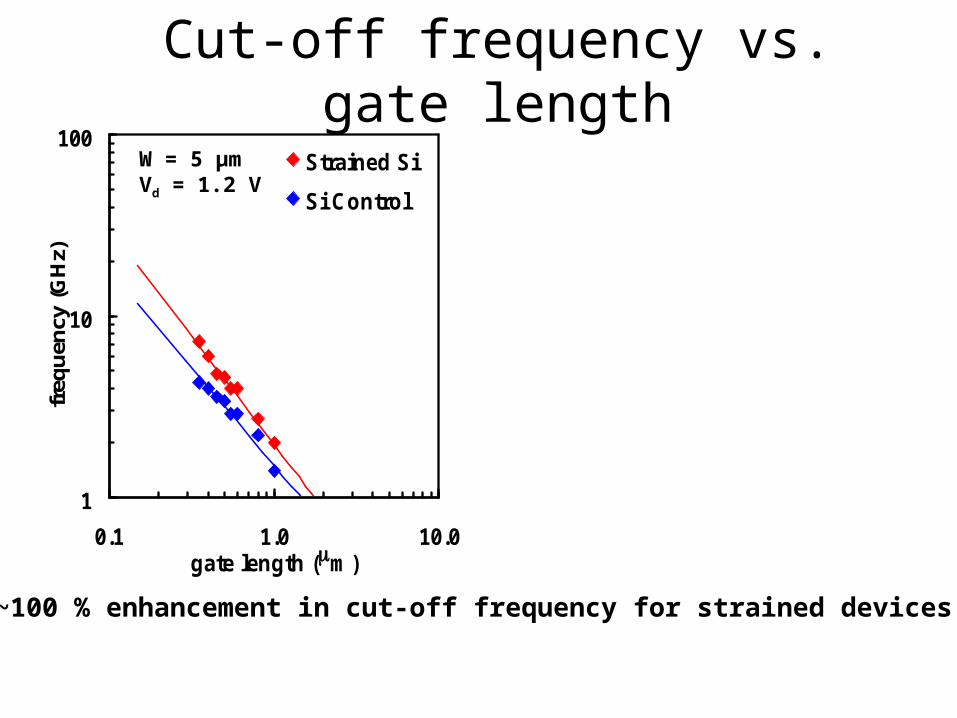
Cut-off frequency vs. gate length
1
10
100
0.1 1.0 10.0gate length (m)
freq
uen
cy (
GH
z)
Strained Si
Si Control
~100 % enhancement in cut-off frequency for strained devices
W = 5 μm Vd = 1.2 V

Cut-off frequency vs. gate length
1
10
100
0.1 1.0 10.0gate length (m)
freq
uen
cy (
GH
z)
Strained Si
Si Control
~100 % enhancement in cut-off frequency for strained devicesgate width increases cut-off frequencyde-embedded pads (not circuit model)
1.0
1.5
2.0
2.5
3.0
0 10 20 30 40 50 60gate width (m)
freq
uen
cy (
GH
z)
Strained Si
Si Control
W = 5 μm Vd = 1.2 V
Lg = 1 μm Vd = 1.2 V
Summary
• First thin virtual substrate MOSFETs
• Enhanced performance
• reduced self heating (cf thick VS)
• RF performance demonstrated