advantages of low beam energies in a tem for valence eels
TRANSCRIPT

Journal of Physics Conference Series
OPEN ACCESS
Advantages of low beam energies in a TEM forvalence EELSTo cite this article M Stoumlger-Pollach and P Pongratz 2010 J Phys Conf Ser 209 012031
View the article online for updates and enhancements
You may also likeChallenging chemical concepts throughcharge density of molecules and crystalsCarlo Gatti
-
Coherent delocalization views ofentanglement in different scenariosR de J Leoacuten-Montiel A Valleacutes H M Moya-Cessa et al
-
Quantum mechanics of excitation transportin photosynthetic complexes a key issuesreviewFederico Levi Stefano MostardaFrancesco Rao et al
-
This content was downloaded from IP address 11493184102 on 12032022 at 0939
Advantages of low beam energies in a TEM for valence EELS
M Stoumlger-Pollach1 and P Pongratz
2
1University Service Centre for TEM Vienna University of Technology
Wiedner Hauptstr 8-10052 A-1040 Vienna AUSTRIA 2Institut fuumlr Festkoumlrperphysik Vienna University of Technology
Wiedner Hauptstr 8-10138 A-1040 Vienna AUSTRIA
Email stoegerustemtuwienacat
Abstract Since the availability of monochromators in transmission electron microscopes
(TEMs) electron energy loss spectrometry (EELS) is widely used to determine band gaps and
the dielectric properties of semiconductors on a nano-metre scale Nevertheless three physical
effects hamper straightforward analysis (a) relativistic energy losses (b) the delocalization of
the energy loss which is in the 10 nano-metreer range for valence losses and (c) the presence
of interface plasmons When reducing the operation voltage of the TEM one can kill two birds
with one stone (a) the relativistic losses will disappear as soon as veltc0n (with ve as the speed
of the electron c0 as the vacuum speed of light and n as the refractive index of the investigated
sample) and (b) the delocalization will decrease because it also depends on the energy of the
incident electron probe The determination of the optical properties of quantum structures is
discussed in the case of GaPGaAs interface at 200 keV and 20 keV beam energy respectively
Further the influence of the delocalization of the energy loss signal is discussed theoretically
and experimentally
1 Introduction Using low beam energies in transmission electron microscopy (TEM) has a long tradition in biological
samples This has a few reasons i) beam damage is reduced because the energy of the probe electron
is reduced ndash and usually biological samples are very beam sensitive ndash ii) due to the fact that biological
samples have a large Carbon content the mean free path for inelastic scattering is very low this means
that even samples of a thickness in the range of 70-100 nm can be easily trespassed by electrons
accelerated with 80 kV and iii) when the incident electron energy is reduced and the mean free path
for inelastically scattered electrons is decreased the contrast in the image is enhanced Beside
advantages like reducing beam damage and enhancing contrast also two big disadvantages are coming
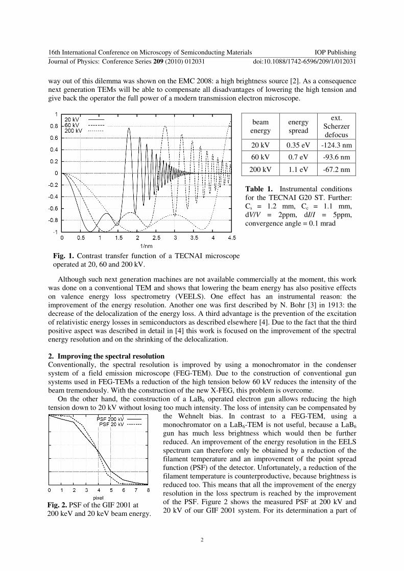
up when reducing the beam energy First the resolution of the microscope is reduced This is shown
in Fig 1 where the contrast transfer function (CTF) of a TECNAI G20 microscope equipped with a
super twin lens and a LaB6 electron source is plotted In all cases the extended Scherzer defocus was
selected For biological samples the CTF seems to be still good enough but in materials science
efforts need to be done in order to bring it back to the high resolution regime First successful results
were presented on the European Microscopy Conference 2008 (EMC 2008) where a Cs corrected high
resolution images recorded at 30 kV was shown [1] The second disadvantage is the decrease of
brightness when reducing the operation voltage of the TEM Little brightness automatically means that
image recording times increase and drift and other instabilities also need to be considered Again a
16th International Conference on Microscopy of Semiconducting Materials IOP PublishingJournal of Physics Conference Series 209 (2010) 012031 doi1010881742-65962091012031
ccopy 2009 IOP Publishing Ltd 1
way out of this dilemma was shown on the EMC 2008 a high brightness source [2] As a consequence
next generation TEMs will be able to compensate all disadvantages of lowering the high tension and
give back the operator the full power of a modern transmission electron microscope
Although such next generation machines are not available commercially at the moment this work
was done on a conventional TEM and shows that lowering the beam energy has also positive effects
on valence energy loss spectrometry (VEELS) One effect has an instrumental reason the
improvement of the energy resolution Another one was first described by N Bohr [3] in 1913 the
decrease of the delocalization of the energy loss A third advantage is the prevention of the excitation
of relativistic energy losses in semiconductors as described elsewhere [4] Due to the fact that the third
positive aspect was described in detail in [4] this work is focused on the improvement of the spectral
energy resolution and on the shrinking of the delocalization
2 Improving the spectral resolution Conventionally the spectral resolution is improved by using a monochromator in the condenser
system of a field emission microscope (FEG-TEM) Due to the construction of conventional gun
systems used in FEG-TEMs a reduction of the high tension below 60 kV reduces the intensity of the
beam tremendously With the construction of the new X-FEG this problem is overcome
On the other hand the construction of a LaB6 operated electron gun allows reducing the high
tension down to 20 kV without losing too much intensity The loss of intensity can be compensated by
the Wehnelt bias In contrast to a FEG-TEM using a
monochromator on a LaB6-TEM is not useful because a LaB6
gun has much less brightness which would then be further
reduced An improvement of the energy resolution in the EELS
spectrum can therefore only be obtained by a reduction of the
filament temperature and an improvement of the point spread
function (PSF) of the detector Unfortunately a reduction of the
filament temperature is counterproductive because brightness is
reduced too This means that all the improvement of the energy
resolution in the loss spectrum is reached by the improvement
of the PSF Figure 2 shows the measured PSF at 200 kV and
20 kV of our GIF 2001 system For its determination a part of
Fig 1 Contrast transfer function of a TECNAI microscope
operated at 20 60 and 200 kV
beam
energy
energy
spread
ext
Scherzer
defocus
20 kV 035 eV -1243 nm
60 kV 07 eV -936 nm
200 kV 11 eV -672 nm
Table 1 Instrumental conditions
for the TECNAI G20 ST Further
Cs = 12 mm Cc = 11 mm
dVV = 2ppm dII = 5ppm
convergence angle = 01 mrad
Fig 2 PSF of the GIF 2001 at
200 keV and 20 keV beam energy
16th International Conference on Microscopy of Semiconducting Materials IOP PublishingJournal of Physics Conference Series 209 (2010) 012031 doi1010881742-65962091012031
2
the CCD was blocked in order to have a knife-edge in
the energy dispersive direction Then the CCD was
illuminated homogeneously and the PSF was measured
The positive effect of the improved PSF on the energy
resolution can be directly measured when the full width
at half maximum (FWHM) of the zero loss peak (ZLP)
is measured Figure 3 shows the ZLPs recorded at
200 kV and 20 kV respectively The FWHM of the
ZLP is reduced to 035 eV instead of 11 eV when the
TEM is operated at 200 kV
3 Delocalization in EELS at low beam energies Besides an improvement of the energy resolution in the EELS
spectrum a reduction of the delocalization of the energy loss is
induced when the beam energy is decreased Figure 4 shows the
reduction of delocalization at low beam energies in comparison
to 100 keV and 200 keV electron beams using once Bohrrsquos cut-
off criterion [3] and once the Rayleigh criterion [5] The Rayleigh
criterion seems to be very crude because it does not include
Coulomb interaction The resulting values are about five times
larger than those obtained by using Bohrrsquos cut-off criterion
Common for both models is that the delocalization is reduced by
a factor of approximately 3 when using 20 keV instead of 200
keV electrons Comparing Bohrrsquos cut-off criterion with a
quantum mechanical model [6] shows an excellent agreement
4 Experimental results For the experimental determination of the optical properties of GaP and GaAs respectively a valence
EELS (VEELS) spectrum image was recorded across the GaPGaAs interface This has the advantage
that the phenomena of i) delocalization and ii) interface plasmon excitation can be studied
simultaneously
41 Delocalization
For the VEELS experiments an FEI TECNAI G20 equipped with a GIF 2001 system was operated at
200 kV and 20 kV The GaPGaAs interface was rotated parallel to the energy dispersive axis of the
spectrometer using a double tilt rotation holder allowing recording a ∆E-r pattern (Figure 5 left side)
On the right hand-side of Figure 5 it can clearly be seen that for the 200 kV experiment the
delocalization is in the range of 10 nm as given by Bohrrsquos cut-off criterion Although the signal is
much more noisy for the 20 kV experiment the delocalization can be estimated to be roughly 4 nm
which is also in good agreement with calculations This experimental test has a fundamental
Fig 5 left Spectrum
image of the GaPGaAs
interface at 200 kV and
20 kV at 164 eV
energy loss (see arrow)
right Normalized
intensity profiles at the
GaP plasmon maximum
for the determination of
the delocalization of the
energy loss
Fig 4 Reduction of
delocalization compared to 100
keV and 200 keV electrons for
an energy loss of 164 eV
Fig 3 Zero
loss peaks
recorded with
200 keV and
20 keV beam
energy
16th International Conference on Microscopy of Semiconducting Materials IOP PublishingJournal of Physics Conference Series 209 (2010) 012031 doi1010881742-65962091012031
3
importance for the determination of the optical properties of non-isolated quantum structures using
200 keV electrons a simple Kramers-Kronig Analysis of VEELS experiments is failing Besides the
influence of relativistic effects [5] delocalization also hampers VEELS analysis of nano-objects using
highly energetic electrons
42 Interface plasmons
Besides delocalization and relativistic energy losses a third feature is altering the VEELS signal the
interface plasmon Due to the fact that interface plasmons (IPs) are at lower energies than volume
plasmons the delocalization of these collective oscillations is even stronger Figure 6 (left) shows the
calculated position of the IP at the GaAsGaP interface In the non-relativistic formalism for a flat
interface between materials A and B with the complex dielectric functions εA and εB the contribution
of the IP is proportional to Im[(εA- εB)(εA+ εB)] Strong IPs are expected when Re(εA+ εB) = 0 and
may produce loss signals below the band gap energy For the present interface the maximum of the IP
is found to be 34 eV (Figure 6 left hand-side) Bohrrsquos cut-off criterion gives a delocalization of this
energy loss of 55 nm for 200 keV and still 20 nm for 20 keV probe electrons This is shown in
Figure 6 on the right hand-side
5 Conclusion The recent experiment demonstrated that the determination of band gaps and dielectric properties of
buried quantum structures is still erroneous when using TEM-EELS applications Although the
delocalization can be decreased by decreasing the beam energy and also relativistic effect can be
avoided completely the appearance of IPs hampers straightforward analyses Even in the case of an
interface between two materials with similar dielectric functions ndash as the GaAsGaP interface ndash IPs
can be detected
Acknowledgements
The Hochschuljubilaumlumsstiftung der Stadt Wien contract Nbr H-015852007 is kindly acknowledged
for funding
References
[1] Freitag B 2008 EMC Technical lecture from FEI company Where are we on abberation
correction and where do we go next
[2] Freitag B et al 2008 Proc EMC 2008 Vol 1 Instrumentation and Methods pp 55-56 M
Luysberg K Tillmann T Weirich (Eds) Springer Verlag Berlin-Heidelberg 2008
[3] Bohr N 1913 Phil Mag 25 10
[4] Stoumlger-Pollach M 2008 Micron 39 1092
Stoumlger-Pollach M et al 2007 Springer Proc in Phys 120 Microscopy of Semiconducting
Materials 2007 pp 345-348 AG Cullis P Midgley (Eds)
[5] Lord Rayleigh 1896 Phil Mag 5 167
[6] Muller DA and Silcox J 1995 Ultramicroscopy 59 195
Fig 6 left Energy loss
contribution to the IP of the
GaAsGaP interface The
negative values at the
volume plasmon position
are due to the begrenzungs-
effekt
right Intensity profile of
the spectrum images at
34plusmn03 eV showing the
delocalization of the IP
16th International Conference on Microscopy of Semiconducting Materials IOP PublishingJournal of Physics Conference Series 209 (2010) 012031 doi1010881742-65962091012031
4

Advantages of low beam energies in a TEM for valence EELS
M Stoumlger-Pollach1 and P Pongratz
2
1University Service Centre for TEM Vienna University of Technology
Wiedner Hauptstr 8-10052 A-1040 Vienna AUSTRIA 2Institut fuumlr Festkoumlrperphysik Vienna University of Technology
Wiedner Hauptstr 8-10138 A-1040 Vienna AUSTRIA
Email stoegerustemtuwienacat
Abstract Since the availability of monochromators in transmission electron microscopes
(TEMs) electron energy loss spectrometry (EELS) is widely used to determine band gaps and
the dielectric properties of semiconductors on a nano-metre scale Nevertheless three physical
effects hamper straightforward analysis (a) relativistic energy losses (b) the delocalization of
the energy loss which is in the 10 nano-metreer range for valence losses and (c) the presence
of interface plasmons When reducing the operation voltage of the TEM one can kill two birds
with one stone (a) the relativistic losses will disappear as soon as veltc0n (with ve as the speed
of the electron c0 as the vacuum speed of light and n as the refractive index of the investigated
sample) and (b) the delocalization will decrease because it also depends on the energy of the
incident electron probe The determination of the optical properties of quantum structures is
discussed in the case of GaPGaAs interface at 200 keV and 20 keV beam energy respectively
Further the influence of the delocalization of the energy loss signal is discussed theoretically
and experimentally
1 Introduction Using low beam energies in transmission electron microscopy (TEM) has a long tradition in biological
samples This has a few reasons i) beam damage is reduced because the energy of the probe electron
is reduced ndash and usually biological samples are very beam sensitive ndash ii) due to the fact that biological
samples have a large Carbon content the mean free path for inelastic scattering is very low this means
that even samples of a thickness in the range of 70-100 nm can be easily trespassed by electrons
accelerated with 80 kV and iii) when the incident electron energy is reduced and the mean free path
for inelastically scattered electrons is decreased the contrast in the image is enhanced Beside
advantages like reducing beam damage and enhancing contrast also two big disadvantages are coming
up when reducing the beam energy First the resolution of the microscope is reduced This is shown
in Fig 1 where the contrast transfer function (CTF) of a TECNAI G20 microscope equipped with a
super twin lens and a LaB6 electron source is plotted In all cases the extended Scherzer defocus was
selected For biological samples the CTF seems to be still good enough but in materials science
efforts need to be done in order to bring it back to the high resolution regime First successful results
were presented on the European Microscopy Conference 2008 (EMC 2008) where a Cs corrected high
resolution images recorded at 30 kV was shown [1] The second disadvantage is the decrease of
brightness when reducing the operation voltage of the TEM Little brightness automatically means that
image recording times increase and drift and other instabilities also need to be considered Again a
16th International Conference on Microscopy of Semiconducting Materials IOP PublishingJournal of Physics Conference Series 209 (2010) 012031 doi1010881742-65962091012031
ccopy 2009 IOP Publishing Ltd 1
way out of this dilemma was shown on the EMC 2008 a high brightness source [2] As a consequence
next generation TEMs will be able to compensate all disadvantages of lowering the high tension and
give back the operator the full power of a modern transmission electron microscope
Although such next generation machines are not available commercially at the moment this work
was done on a conventional TEM and shows that lowering the beam energy has also positive effects
on valence energy loss spectrometry (VEELS) One effect has an instrumental reason the
improvement of the energy resolution Another one was first described by N Bohr [3] in 1913 the
decrease of the delocalization of the energy loss A third advantage is the prevention of the excitation
of relativistic energy losses in semiconductors as described elsewhere [4] Due to the fact that the third
positive aspect was described in detail in [4] this work is focused on the improvement of the spectral
energy resolution and on the shrinking of the delocalization
2 Improving the spectral resolution Conventionally the spectral resolution is improved by using a monochromator in the condenser
system of a field emission microscope (FEG-TEM) Due to the construction of conventional gun
systems used in FEG-TEMs a reduction of the high tension below 60 kV reduces the intensity of the
beam tremendously With the construction of the new X-FEG this problem is overcome
On the other hand the construction of a LaB6 operated electron gun allows reducing the high
tension down to 20 kV without losing too much intensity The loss of intensity can be compensated by
the Wehnelt bias In contrast to a FEG-TEM using a
monochromator on a LaB6-TEM is not useful because a LaB6
gun has much less brightness which would then be further
reduced An improvement of the energy resolution in the EELS
spectrum can therefore only be obtained by a reduction of the
filament temperature and an improvement of the point spread
function (PSF) of the detector Unfortunately a reduction of the
filament temperature is counterproductive because brightness is
reduced too This means that all the improvement of the energy
resolution in the loss spectrum is reached by the improvement
of the PSF Figure 2 shows the measured PSF at 200 kV and
20 kV of our GIF 2001 system For its determination a part of
Fig 1 Contrast transfer function of a TECNAI microscope
operated at 20 60 and 200 kV
beam
energy
energy
spread
ext
Scherzer
defocus
20 kV 035 eV -1243 nm
60 kV 07 eV -936 nm
200 kV 11 eV -672 nm
Table 1 Instrumental conditions
for the TECNAI G20 ST Further
Cs = 12 mm Cc = 11 mm
dVV = 2ppm dII = 5ppm
convergence angle = 01 mrad
Fig 2 PSF of the GIF 2001 at
200 keV and 20 keV beam energy
16th International Conference on Microscopy of Semiconducting Materials IOP PublishingJournal of Physics Conference Series 209 (2010) 012031 doi1010881742-65962091012031
2
the CCD was blocked in order to have a knife-edge in
the energy dispersive direction Then the CCD was
illuminated homogeneously and the PSF was measured
The positive effect of the improved PSF on the energy
resolution can be directly measured when the full width
at half maximum (FWHM) of the zero loss peak (ZLP)
is measured Figure 3 shows the ZLPs recorded at
200 kV and 20 kV respectively The FWHM of the
ZLP is reduced to 035 eV instead of 11 eV when the
TEM is operated at 200 kV
3 Delocalization in EELS at low beam energies Besides an improvement of the energy resolution in the EELS
spectrum a reduction of the delocalization of the energy loss is
induced when the beam energy is decreased Figure 4 shows the
reduction of delocalization at low beam energies in comparison
to 100 keV and 200 keV electron beams using once Bohrrsquos cut-
off criterion [3] and once the Rayleigh criterion [5] The Rayleigh
criterion seems to be very crude because it does not include
Coulomb interaction The resulting values are about five times
larger than those obtained by using Bohrrsquos cut-off criterion
Common for both models is that the delocalization is reduced by
a factor of approximately 3 when using 20 keV instead of 200
keV electrons Comparing Bohrrsquos cut-off criterion with a
quantum mechanical model [6] shows an excellent agreement
4 Experimental results For the experimental determination of the optical properties of GaP and GaAs respectively a valence
EELS (VEELS) spectrum image was recorded across the GaPGaAs interface This has the advantage
that the phenomena of i) delocalization and ii) interface plasmon excitation can be studied
simultaneously
41 Delocalization
For the VEELS experiments an FEI TECNAI G20 equipped with a GIF 2001 system was operated at
200 kV and 20 kV The GaPGaAs interface was rotated parallel to the energy dispersive axis of the
spectrometer using a double tilt rotation holder allowing recording a ∆E-r pattern (Figure 5 left side)
On the right hand-side of Figure 5 it can clearly be seen that for the 200 kV experiment the
delocalization is in the range of 10 nm as given by Bohrrsquos cut-off criterion Although the signal is
much more noisy for the 20 kV experiment the delocalization can be estimated to be roughly 4 nm
which is also in good agreement with calculations This experimental test has a fundamental
Fig 5 left Spectrum
image of the GaPGaAs
interface at 200 kV and
20 kV at 164 eV
energy loss (see arrow)
right Normalized
intensity profiles at the
GaP plasmon maximum
for the determination of
the delocalization of the
energy loss
Fig 4 Reduction of
delocalization compared to 100
keV and 200 keV electrons for
an energy loss of 164 eV
Fig 3 Zero
loss peaks
recorded with
200 keV and
20 keV beam
energy
16th International Conference on Microscopy of Semiconducting Materials IOP PublishingJournal of Physics Conference Series 209 (2010) 012031 doi1010881742-65962091012031
3
importance for the determination of the optical properties of non-isolated quantum structures using
200 keV electrons a simple Kramers-Kronig Analysis of VEELS experiments is failing Besides the
influence of relativistic effects [5] delocalization also hampers VEELS analysis of nano-objects using
highly energetic electrons
42 Interface plasmons
Besides delocalization and relativistic energy losses a third feature is altering the VEELS signal the
interface plasmon Due to the fact that interface plasmons (IPs) are at lower energies than volume
plasmons the delocalization of these collective oscillations is even stronger Figure 6 (left) shows the
calculated position of the IP at the GaAsGaP interface In the non-relativistic formalism for a flat
interface between materials A and B with the complex dielectric functions εA and εB the contribution
of the IP is proportional to Im[(εA- εB)(εA+ εB)] Strong IPs are expected when Re(εA+ εB) = 0 and
may produce loss signals below the band gap energy For the present interface the maximum of the IP
is found to be 34 eV (Figure 6 left hand-side) Bohrrsquos cut-off criterion gives a delocalization of this
energy loss of 55 nm for 200 keV and still 20 nm for 20 keV probe electrons This is shown in
Figure 6 on the right hand-side
5 Conclusion The recent experiment demonstrated that the determination of band gaps and dielectric properties of
buried quantum structures is still erroneous when using TEM-EELS applications Although the
delocalization can be decreased by decreasing the beam energy and also relativistic effect can be
avoided completely the appearance of IPs hampers straightforward analyses Even in the case of an
interface between two materials with similar dielectric functions ndash as the GaAsGaP interface ndash IPs
can be detected
Acknowledgements
The Hochschuljubilaumlumsstiftung der Stadt Wien contract Nbr H-015852007 is kindly acknowledged
for funding
References
[1] Freitag B 2008 EMC Technical lecture from FEI company Where are we on abberation
correction and where do we go next
[2] Freitag B et al 2008 Proc EMC 2008 Vol 1 Instrumentation and Methods pp 55-56 M
Luysberg K Tillmann T Weirich (Eds) Springer Verlag Berlin-Heidelberg 2008
[3] Bohr N 1913 Phil Mag 25 10
[4] Stoumlger-Pollach M 2008 Micron 39 1092
Stoumlger-Pollach M et al 2007 Springer Proc in Phys 120 Microscopy of Semiconducting
Materials 2007 pp 345-348 AG Cullis P Midgley (Eds)
[5] Lord Rayleigh 1896 Phil Mag 5 167
[6] Muller DA and Silcox J 1995 Ultramicroscopy 59 195
Fig 6 left Energy loss
contribution to the IP of the
GaAsGaP interface The
negative values at the
volume plasmon position
are due to the begrenzungs-
effekt
right Intensity profile of
the spectrum images at
34plusmn03 eV showing the
delocalization of the IP
16th International Conference on Microscopy of Semiconducting Materials IOP PublishingJournal of Physics Conference Series 209 (2010) 012031 doi1010881742-65962091012031
4