aedc-tr-73-116 laser velocimetry data processing aedc-tr-73-116 laser velocimetry data processing h....
TRANSCRIPT

AEDC-TR-73-116
LASER VELOCIMETRY DATA PROCESSING
H. T. Kalb, D. B. Brayton, and J. A. McClure
ARO, Inc.
September 1973
AP£ roved for public release; distribution unlimited.
ARNOLD ENGINEERING DEVELOPMENT CENTER
AIR FORCE SYSTEMS COMMAND
ARNOLD AIR FORCE STATION, TENNESSEE

NOTICES When U. S. Government drawings specifications, or other data are used for any purpose other than a definitely related Government procurement operation, the Government thereby incurs no responsibility nor any obligation whatsoever, and the fact that the Government may have formulated, furnished, or in any wav supplied the said drawings, specifications, or other data, is not to be regarded by implication or otherwise, or in any manner licensing the holder or any other person or corporation, or conveying any rights or permission to manufacture, use. or sell any patented invention that may in any way be related thereto.
Qualified users may obtain copies of this report from the Defense Documentation Center.
References to named commercial products in this report are not to be considered in any sense as an endorsement of the product by the United States Air Force or the Government.

AEDC-tR-73-iliS
LASER VELOCIMETRY DATA PROCESSING
H. T. Kalb, D. B. Brayton, and J. A. McClure
AtK>\ Inc.
Approved for public release: distribution unlimited.
AEDC-TR-73-116
FOREWORD
The research reported herein was done by the Arnold Engineering Development Center (AEDC), Air Force Systems Command (AFSC), under Program Element 65802F. The results were obtained by ARO, Inc. (a subsidiary of Sverdrup & Parcel and Associates, Inc.), contract operator of the AEDC, Arnold Air Force Station, Tennessee.
The research and development of an instrument for processing fre- quency burst data has been conducted from 1969 to 1973 under ARO Project No. BF319-12YA. This report, submitted for publication on May 11, 1973, describes the instrument and its application to low signal-to-noise-ratio signal areas.
The authors wish to acknowledge the able assistance and leader- ship of A. E. Lennert, project manager. Further acknowledgement is made to B. J. McClure for prototype fabrication and testing.
This technical report has been reviewed and is approved.
MELVIN L. GUIOU ROBERT O. DIETZ Captain, USAF Director of Technology Research and Development Division Directorate of Technology
li
AEDC-TR-73-116
ABSTRACT
The development of instrumentation for capture and processing of low signal density "frequency burst" data produced by a laser veloci- meter is described. This signal type typically occurs at high flow rates and/or with no artificial seeding. The extension of the instru- ment application into poor signal-to-noise areas is described.
111

AEDC-TR-73-116
CONTENTS
Page
ABSTRACT iii I. INTRODUCTION 1
II. LASER VELOCIMETER DATA PROCESSOR SYSTEM DESCRIPTION 2. 1 Selective Capture of Frequency Burst Signal Data . . 2 2. 2 Processor Block Diagram 3 2. 3 Time Interval Comparator 4 2. 4 Dual Time Interval Comparison 5 2. 5 "Data Accept" Recycle Sequence 5 2. 6 "Data Reject" Recycle Sequence 6 2. 7 Data in Binary Coded Decimal Form 6 2. 8 Processor Sample Rate 7 2. 9 Extended Frequency Coverage 7
III. LV PROCESSOR DATA HANDLING 3. 1 Digital Printer and Mag Tape Recorder 9 3. 2 Data Compression 10 3. 3 Analog Recording of Time Dependent Data 10 3.4 Multi-Component Processing of Simultaneous Data . . 11 3.5 Video Tape Frequency Burst Test Generator 11
IV. LV FREQUENCY BURST SIGNAL SYNTHESIZER 12 REFERENCES 14
APPENDIXES
I. ILLUSTRATIONS
Figure
1. Frequency Burst Waveforms a. Ideal Velocimeter Burst Waveform 17 b. Noise Superimposed on Waveform 17 c. Large Amplitude Noise on Burst Signal 17 d. Zero Crossing Detector Output for Low S/N
Signal 17
2. Alias Reading Distribution Obtained from Low S/N Signal Data; Input S/N Power Ratio = 0. 07; Signal Level 9mv (rms) at 250 kHz; Noise Level 34 mv (rms) 18
AEDC-TR-73-116
Figure Page
3. Alias Reading Distribution Obtained from Low S/N Signal Data; Input S/N Power Ratio = 0. 09; Signal Level 15 mv (rms) at 100 kHz; Noise Level 50 mv (rms) 19
4. Processor Performance in Low S/N Signal Areas .... 20
5. Laser Velocimeter Data Processor Block Diagram ... 21
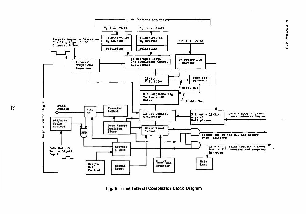
6. Time Interval Comparator Block Diagram 22
7. Time Dependent Directional Burst Data at a 5-kHz Rate . 23
8. Pulse Stretcher Diagram 24
9. Memory Formatted Data Display 25
10. Reconstructed Burst Signal from Video Tape 26
11. Schematic Diagram of an LV Signal Synthesizer 27
12. Synthesized Burst Signal Waveform 28
13. Laser Velocimeter Data Processor Photograph 29
II. TABLES
I. Computer Printout of Error Analysis for 4/5/8 Time Interval Comparator 30
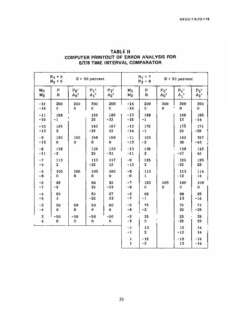
II. Computer Printout of Error Analysis for 6/7/8 Time Interval Comparator 31
III. Specific Pulse Pattern Required to Permit Multiple TIC Test to Fail and Alias Reading to be Printed . 32
III. ANALYSIS OF THE DUAL TIME INTERVAL COMPARATOR TEST 33
VI

AEDC-TR-73-116
SECTION I INTRODUCTION
The development of an instrument system for processing signals generated by a laser velocimeter is described. The design effort, since 1969, has been directed toward the real time measurement of high velocity unseeded flow media.
An early prototype version of the processor was employed in 1970 to successfully capture "burst" data produced by a velocimeter, mon- itoring an intrinsic seeded air stream at velocities to Mach number 1. 5. The results of this test have been reported (Refs. 1 and 2). The processor has subsequently been employed in tests measuring air speeds in excess of 7000 feet per second.
The present data processor employes a novel form of digital error detecting data acquisition system. The use of this technique has per- mitted the processing of LDV-derived frequency burst data in signal- to-noise-ratio areas an order of magnitude lower than had formerly been practical.
This report will discuss the processor currently being employed in AEDC wind tunnel tests and various methods that have been em- ployed in data handling.
SECTION II LASER VELOCIMETER DATA PROCESSOR SYSTEM DESCRIPTION
The use of a laser velocimeter in producing frequency burst data from intrinsic airstream entrained dust particles has been described in the literature (Ref. 2). It has been shown how two laser beams with mutually coherent and like-polarized radiation, when permitted to cross, establish planar interference fringes in the crossover region. The plane parallel intereference fringes provide regions of maximum and minimum illuminating intensity. As a moving dust particle passes through the crossbeam region it will intercept the interference fringes and the illumination level it experiences will alternate from maximum to minimum. If a suitable optical system is provided to couple the crossbeam region to a photosensitive detector, such as a photomulti- plier tube, the detector will provide an analog signal proportional to

AEDC-TR-73-116
the amount of light collected from the dust particle. The detector will produce an amplitude fluctuating signal proportional to the rate at which the particle intercepts the fringes. The particle velocity normal to the fringe plane can then be determined from the fringe plane spacing and the averaged time interval required to traverse between fringe planes.
2.1 SELECTIVE CAPTURE OF FREQUENCY BURST SIGNAL DATA
The data processor samples eight pulse periods of the limited du- ration "burst" waveform and digitizes the resultant time interval via period counter techniques. Time intervals as short as 80 nanoseconds may be quantized at rates of 50, 000 samples per second. In the pres- ence of poor signal-to-noise ratios, the burst signal sustains severe waveform aberrations that impede the extraction of the desired time period data. The signal suffers both pulse dropouts and pulse addi- tions attributable to noise cancellation of signal information. The processor employs high-speed digital computing circuitry to test the data pulse train for periodicity; it compares the time interval of both four and five data pulses (or oscillation periods) to the time interval of eight data pulses. The eight-pulse interval has been chosen to ac- commodate the short duration signal type dictated by the velocimeter optics design. The two-stage time interval comparison is necessary when sampling low S/N data since pulse dropouts and pulse additions can, in certain combinations, produce pulse trains that will appear to be periodic when inspected by only a single test. With a single test comparison, low S/N data produces alias or false readings that differ widely from the true readings. For example, the 4/8 time interval test typically permits alias readings that are ±25, ±50, ±75, and ±100 percent of the true reading; the 5/8 test typically permits alias read- ings of ±37. 5, -18, -31, +62.5, and ±100 percent. With a dual time interval test, simultaneous erroneous readings seldom occur thereby permitting dual test rejection to be highly successful.
The advantages of data acquisition employing a dual time interval test are clearly indicated in Figs. 1 through 4 (Appendix I). Figure la illustrates an ideal frequency burst waveform. Figures lb and c show a progressive increasing noise content added to the burst signal wave- form. Figure Id illustrates the data pulse train output from the zero crossing detector when the signal lc is processed. It is this signal type, with dropout and added noise pulses shown, from which was ob- tained the printed data distributions shown in Figs. 2 and 3. Each test employed a series of one thousand samples presented simultaneously
AEDC-TR-73-116
to three processors equipped with different error detecting logic. One processor was equipped with a 4/8 time interval comparator (TIC) test only, a second processor was equipped with a 5/8 interval comparator test only, and a third processor was equipped with a dual two-step (4/8 and 5/8) comparator test. The resultant distribution of true and false (alias) readings obtained from the three processors is plotted. It can be seen that the dual test permits a marked imporvement in the resulting data quality by the elimination of most of the false or alias readings. Figure 4 illustrates the dual comparator processor's per- formance when presented with a series of input signals having a pro- gressively lower signal-to-noise ratio. The processor data capture ratio begins to drop sharply for S/N ratio values below 0. 20; however, the quality of the printed data remains high for capture ratios below 1 percent of total sample cycles.
2.2 PROCESSOR BLOCK DIAGRAM
Figures 5 and 6 illustrate the data processor in block form. The circuit shown is usable for capture of frequency burst data over the range of 1 kHz to 500 kHz. A method for extended coverage to fre- quencies above 500 kHz is discussed in Section 2. 9.
The burst data are shown entering the multiband analog filter with simultaneous display on an oscilloscope. The filter removes the ped- estal (lower frequency component) and provides nine filter bands from 1-kHz to 50-MHz frequency coverage. High-speed, emitter-coupled - logic, integrated circuitry is employed in both the filter output zero crossing detector and the sampling binaries A through D. The latter converts the eight signal oscillations into an equivalent time interval pulse (rectangle wave) denoted as the 'D" pulse. Simultaneously, time interval pulses are generated by the E^ and E2 binaries. The Ej pulse is equal to the period of the first four data pulses, and the E2 pulse period equals the period of the first five data pulses.
The three time interval pulses, denoted as the D, El and E2, gate three independent counters bearing the same respective designation. These counters serve to quantize the three time intervals; each counter contains a natural binary number representing the corresponding time interval.
AEDC-TR-73-116
2.3 TIME INTERVAL COMPARATOR
The binary numbers are now applied to a hardwired computing cir- cuit (Fig. 5) that first compares the eight-pulse interval "D" to the scaled four-pulse interval Ei, and subsequently compares the eight- pulse interval to the scaled five-pulse interval E2. A scale factor of eight to four is applied to the four-pulse interval by hardwire multiply- ing the binary number contained in the Ej (four pulse) counter by two. Thus, for an ideally periodic input data pulse train the multiplied Ej counter number is equal to the D counter number. To detect the dif- ference in the scaled E\ pulse time duration with respect to the D pulse time duration, the two binary numbers are applied to a 17-bit full adder. The Ei counter number is applied in 2's complement form, causing the adder to perform as a subtractor and produce at its output the quantity \D - 2Ej| or the complement of this number. If D is the larger number entered, then the true quantity is obtained from the subtractor; if 2Ei is the larger number, then the result must be re- complemented to obtain the true value.
As the desired result from the subtractor is the magnitude \D - 2Ei| (the sign of the number is unimportant in the final time interval com- parison test), it is necessary to detect when the complement of the number is outputted by the subtractor. This is done by the sign bit detector (Fig. 5) which monitors the carry out terminal of the subtrac- tor. It can be shown that the true value exists when a carry out signal is present. Thus, in the absence of a carry signal, the sign bit de- tector raises the enable bus to a row of exclusive-OR gates which serve as a programmed inverter. When the enable bus is high, the gates recomplement the subtractor output and input to the 13-bit digi- tal comparator the quantity \D - 2Ei|. With a carry signal present, the Ex-OR gates pass the subtractor output direct to the comparator without inversion.
The digital comparator performs a comparison of the magnitude of two numbers producing, at appropriate output terminals, a signal de- noting which is the larger. The second number input to the comparator is a preselected percentage of the eight-pulse interval D counter bi- nary number obtained by simple binary division. This number, de- signated as "KD", becomes the "data window" or the maximum accept- able limit value that the doubled Ej time interval pulse may differ from the D time interval pulse. "KDP is obtained by a divide-by-two sequence in which each time the number receives a right shift of one place (or bit); the resultant number is one-half the quantity of the original number.
AEDC-TR-73-116
As an example, the number 16 expressed in binary form as 010000 be- comes 001000 or eight with a one place right shift. The "KD'1 binary number has been wired to the digital comparator input through a multi- plexer to permit a selective division by 32, 64, or 128. The resultant number represents 3. 0 percent, 1, 56 percent, and 0. 78 percent, re- spectively, of the original D counter binary number. When \D - 2Ei|> KD, the digital comparator outputs a signal onto a "data reject1' bus. When "KD" is the larger quantity, the comparator outputs a signal onto a '"data accept" bus.
The time interval comparison test can easily be made within a two-microsecond interval with existing standard TTL integrated cir- cuit logic.
2.4 DUAL TIME INTERVAL COMPARISON
At the termination of the 4/8 pulse time interval test, the data ac- cept decision is stored and the comparator sequence multiplexer auto- matically proceeds with the 5/8 time interval comparison test. The sixteen-bit multiplexer, Fig. 5, switches the contents of the E2 counter into the subtractor in place of the Ej counter number. Similar proce- dural methods to the 4/8 test then follow. The E2 counter binary num- ber is given a hardwired equivalent multiply by 1. 6, is 2's comple- mented, and entered into the subtractor. The percentage of the D counter number "KD" applied to the comparator remains unchanged during the second time interval test. The comparator decision KD > or < |D - 1. 6 E2I now appears on either the "data accept1' or the "data reject" signal line, respectively.
The decisions from the two tests are then compared. If both tests indicate acceptable data, then the "AND"1 decision is applied as a strobe pulse to the data registers within the processor, simultaneously causing (1) the binary register to transfer and store the D counter binary data, and (2) the 20-bit binary coded decimal (BCD) register to transfer and store BCD data from an auxilliary BCD counter. The purpose of the dual registers shall presently be discussed.
2.5 "DATA ACCEPT" RECYCLE SEQUENCE
At the completion of the data transfer strobe pulse, a transfer 1- shot (Fig. 5) and a print command flip-flop are triggered. The flip-flop

AEDC-TR-73-116
issues to an attached data acquisition system. (DAS) a print command and the processor reverts to a standby mode until a further signal ("flag" pulse) is received from the DAS. The termination of the "flag" pulse from the DAS releases the recycle sequence latch by triggering the recycle 1-shot. This 1-shot resets the print command flip-flop, issues a zero reset pulse to all counters, and resets the A through E sampling binaries to their required initial condition state. At reset pulse termination, the processor must further await the reception of a -r-A gate signal from the oscilloscope before a new sample interval may begin.
2.6 "DATA REJECT" RECYCLE SEQUENCE
The recycle sequence is altered when either (1) one or both com- parator tests issue "data reject" signals or (2) the input time interval pulse to the D counter does not lie between preselected Pmin and Pmax
values. Provision is made through the error reset 1-shot to abort the sample interval as soon as one of these data reject signals occur. In this mode of recycle, a print command issue is inhibited, counters are reset to zero, and the oscilloscope triggered gate is given control of the binaries pending a subsequent frequency burst signal event. The Pmax - Pmin detector directly monitors the D counter time interval pulse duration and permits only data that lie between the analog filter minimum and maximum breakpoint frequencies to be passed for time interval comparison.
2.7 DATA IN BINARY CODED DECIMAL FORM
Five numeric indicator (Nixie) tubes are used for the purpose of visually displaying the average period of the sampled data. Data con- version to decimal form can more conventiently be done "on line" when the data exists in binary coded decimal form rather than natural binary form. Further, many DAS are equipped to receive BCD rather than binary. Data in binary form, however, more efficiently uses storage bit capacity and can be employed to advantage when data transfer is made to systems such as mini-computers or magnetic tape recorders. As indicated in Fig. 5, the processor employs a five-digit BCD counter operating in parallel with the 17-bit D counter. Thus, at the termination of a sample interval, register-stored data exist in either natural binary or 8421 weighted BCD. The paralled binary-BCD counters and registers are implemented with standard MSI digital logic and printed circuit

AEDC-TR-73-116
board techniques. The same procedure applies to the time interval comparator and sampling binaries.
2.8 PROCESSOR SAMPLE RATE
The rate at which the processor may sample is determined by (1) the signal burst density (number of bursts per unit time), (2) the time interval of eight signal burst oscillations, (3) the processor recycle time, and (4) the DAS transfer time. For example, if continuous wave (CW) signal information were available at 500 kHz, a sixteen- microsecond sample interval for eight data pulses and an eight- microsecond recycle time would provide a processor sample rate of approximately 40, 000 per second.
Figure 7 illustrates air velocity samples taken at a 5-kHz rate; samples were taken at a fixed point adjacent to a speaker cone oscil- lating at a 146-Hz rate using a velocimeter employing a Bragg cell; the directionality capability of this velocimeter was provided by the Bragg cell optical design. Note that the sampled data are time dependent. Data acquisition was accomplished by direct transfer to an on-line mini-computer with subsequent data reconstruction by Cal-Comp Plotter.
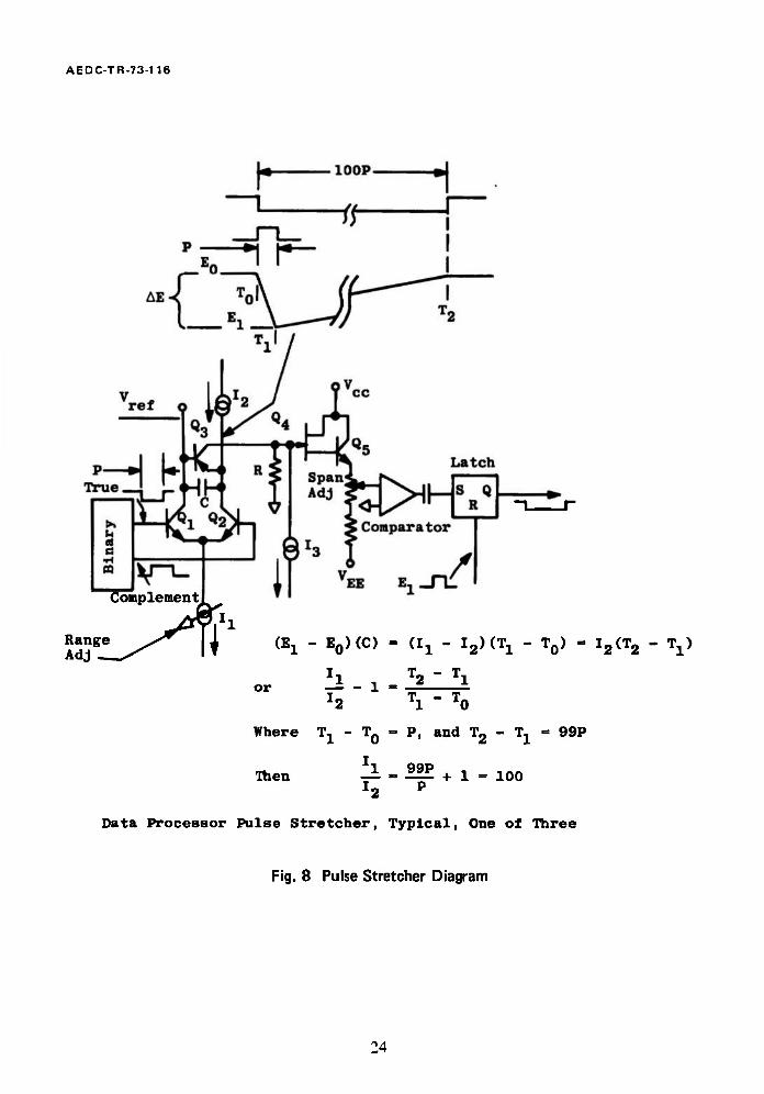
2.9 EXTENDED FREQUENCY COVERAGE
The limited sample interval of eight data pulses imposed by the short duration frequency burst type signals places severe demands on counter resolution at signal frequencies much above 500 kHz. Preci- sion pulse stretchers are employed to extend the time duration of the D and Ei and E2 interval pulses producing resultant counter gating pulses 100 times the duration of the unstretched pulse. This permits the extension of the processor upper limit frequency to 50 MHz.
The pulse stretcher is shown in Fig. 8. Qi and Q2 are high-speed current switches, direct coupled to the true-complement terminals of an ECL flip-flop. Two precision constant current sources, Ii and I2, and a reference voltage at the collector of Qj provide the initial condi- tions for stretch sequence. Qj is on, Q2 off, permitting I2 to cause Q3 to conduct. The initial positive voltage appearing across resistance R has caused the comparator to set the latch with Q at logic "l". At the beginning of a sample interval, the Ei binary (complement terminal)
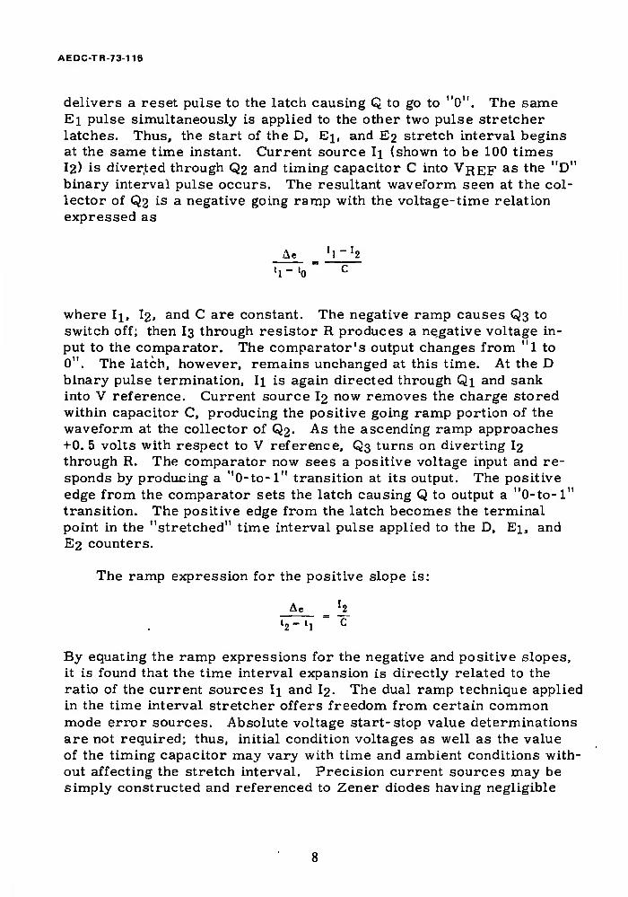
AEDC-TR-73-116
delivers a reset pulse to the latch causing Q to go to "O". The same Ei pulse simultaneously is applied to the other two pulse stretcher latches. Thus, the start of the D, E\, and E2 stretch interval begins at the same time instant. Current source Ii (shown to be 100 times l2) is diverted through Q2 and timing capacitor C into VR^F as the "D" binary interval pulse occurs. The resultant waveform seen at the col- lector of Q2 is a negative going ramp with the voltage-time relation expressed as
'l-'o
where 1^, I2, and C are constant. The negative ramp causes Q3 to switch off; then I3 through resistor R produces a negative voltage in- put to the comparator. The comparator's output changes from "l to 0". The latch, however, remains unchanged at this time. At the D binary pulse termination, Ii is again directed through Qi and sank into V reference. Current source I2 now removes the charge stored within capacitor C, producing the positive going ramp portion of the waveform at the collector of Q2. As the ascending ramp approaches + 0.5 volts with respect to V reference, Q3 turns on diverting I2 through R. The comparator now sees a positive voltage input and re- sponds by producing a "0-to-l" transition at its output. The positive edge from the comparator sets the latch causing Q to output a "0-to-l" transition. The positive edge from the latch becomes the terminal point in the "stretched" time interval pulse applied to the D, Ei, and E2 counters.
The ramp expression for the positive slope is:
l2-li
By equating the ramp expressions for the negative and positive slopes, it is found that the time interval expansion is directly related to the ratio of the current sources Ii and I2. The dual ramp technique applied in the time interval stretcher offers freedom from certain common mode error sources. Absolute voltage start-stop value determinations are not required; thus, initial condition voltages as well as the value of the timing capacitor may vary with time and ambient conditions with- out affecting the stretch interval. Precision current sources may be simply constructed and referenced to Zener diodes having negligible
AEDC-TR-73-1K
temperature coefficients. Calibration of the pulse stretcher is accom- plished by applying a stable frequency source and monitoring the BCD counter/visual display while adjusting calibration potentiometers. Two calibration adjustments are available for each stretcher on each range to achieve best linearity. On-board gating permits routing the three interval pulses to the BCD counter individually during the calibration cycle.
SECTION III LV PROCESSOR DATA HANDLING
A wide variety of digital handling peripheral equipment exists for acquiring, transferring, storing, manipulating, and compressing digi- tal data. The large amount of data that can be produced by a laser velocimeter coupled data processor makes some form of automatic data handling system mandatory.
3.1 DIGITAL PRINTER AND MAG TAPE RECORDER
The simplest approach employs a digital line printer. This in- strument can typically produce a twenty-column, twenty-line per second printout. It has the advantage of producing an on-line hard copy. It has the disadvantage of leaving the printed data in an awk- , ward form for further processing and is inadequate for fast data rates.
A buffered incremental digital tape recorder can increase the data rate to in excess of 1, 000 five digit data point groups per second. The buffer memory of the recorder can accept short duration signal bursts at the maximum rate of 50, 000 per second. The incremental feature is useful since the velocimeter data rate is often subject to erratic variations. A high-speed, continuous run tape system can continuously acquire 6, 000 five digit data points per second and with fast memory buffering achieve rates in excess of 100, 000 data points per second for short intervals. The digital tape recorder offers the advantage of large static storage capacity of data with some ease in recovering the data for digital computer reduction. The method does suffer the dis- advantage of not providing a quick look at the data in progress.
An on-line mini-computer offers a means of short time duration, high data rate acquisition. It may also serve as a buffer for a digital

AEDC-TR-73-116
tape system. The computer is versatile in the type of on-line manipula- tion it can perform on small data groups. The computer can convert the period data of the processor directly to frequency or to velocity units. Data grouping such as rms averaging can be performed, and time cor- relation of data points for subsequent tape storage can be achieved.
3.2 DATA COMPRESSION
A form of data compression may conveniently be exercised upon large data blocks by the use of a "stand alone" memory. Data outputted by the processor over a given frequency range occupies a known range of numbers. A word location in memory is assigned to each number; the number becomes the address for that specific word location. If the memory word is made to store or totalize the number to times it has been addressed, then at the end of a data taking interval the memory contains a distribution of data that can be displayed along a frequency or period scale. The contents of the memory can be serially read out by a counter sequentially addressing each word location within the ori- ginal range of numbers. The memory formatted data might typically appear as in Fig. 9. Data in this form can be block transferred to tape or computer at a considerable savings in data quantity handled. The data period and number of occurrences completely describe the data block when time averaged data is permitted. This is significant at high rates where the limiting factor is the acquisition speed of the re- corder or the memory capacity of the computer. A sequence counter and a pair of D/A converters would permit the stored data to be dis- played on an oscilloscope. The histogram display provides an on-line look at mean velocity variations. Sixty-four thousand occurrences of a given data period can be stored in one 16-bit memory word opposed to only one if the period value is individually recorded. Typical memory cycle time permits recording an occurrence rate in excess of one MHz.
3.3 ANALOG RECORDING OF TIME DEPENDENT DATA
Time dependent data recording at high data rates for extended in- tervals becomes a major task if done digitally. The task becomes worse if three velocity components plus positional data are required. A trade-off can be made by outputting processor data in analog form, employing analog computing techniques to produce velocity information with subsequent data storage in a multi-channel analog recorder. Existing D/A converters and analog dividers provide for conversion
10
AEDC-TR-73-116
rates through 50 kHz. This technique has been locally used for a "quick look" oscilloscope display of a velocimeter system at rates to 30, 000 samples per second. The register-stored data from the proc- essor directly applied to the D/A converter provides for a zero droop sample and hold technique.
3.4 MULTI-COMPONENT PROCESSING OF SIMULTANEOUS DATA
The processor is a single component data sampling device. Si- multaneous capture of multi-component velocimeter data has been ac- complished by multiple processors sampling individual data channels. A common gating signal may be applied to the multiple processors permitting simultaneous sampling of a common particle passage through the probe volume. This method has successfully been employed at AEDC for two-component data. A Hewlett Packard digital scanner and mag- netic tape system was used to handle the data. The scanner was pro- grammed to channel code the data and provide for transfer to the tape only when both component channels produced data.
3.5 VIDEO TAPE FREQUENCY BURST TEST GENERATOR
This device has been used within the lab for the analog recon- struction of velocimeter data. Sample information from an operational velocimeter is first recorded and may later be reconstructed as a test signal for performance testing the processor on the bench. The tape recorded video information offers a wealth of frequency burst signal types and waveform variations. Selection of a specific test signal in- volves the recorder being operated in an unorthodox manner. The tape is maintained stationary and the video reproduce head is permitted to repeatedly scan the same narrow slice of tape. The information con- tained on this slice is equivalent to one horizontal scan on a conven- tional video picture tube, yet it can contain numerous frequency burst signals. The horizontal sync pulse generated by the video recorder is used to trigger the PB'' time base of an oscilloscope. The oscilloscope is then operated in an "A" delayed by "B" time base mode. Selectable segments of the tape video information are then displayed against the A time base. The B time base delay control permits the dialing in of new video information. Thus, a frequency burst signal is selected on the scope display and the scope gate signal to the processor permits the processor to initiate a sample interval. The point along the burst signal where sampling begins is easily changed by the B delay control.
II

AEDC-TR-73-116
Figure 10 illustrates a tape reconstructed waveform.
SECTION IV LV FREQUENCY BURST SIGNAL SYNTHESIZER
The photodetected time domain signal for a single scatter particle traversing a fringe set for the conventional dual scatter LV is given by Ref. 3
N(t) = Ape-(2V2(t-to)/r)2 + ^ e-(2 V'2 (t - to)/r)2 CQS ^
where fj) is the Doppler frequency and T is the time required for the scatter particle to transit the probe volume outer boundary. The boundary is defined as the surface of an ellipsoid where the laser radiation intensity is e~^ times the maximum intensity near the geo- metric center of the probe volume. The signal is seen to consist of two distinct summed waveforms: (1) a Gaussian pedestal waveform with peak amplitude Ap, and (2) a Gaussian amplitude modulated sinu- soid with peak amplitude As.
A circuit used to synthesize the waveform described is shown in Fig. 11. Linear and digital integrated circuits are employed where possible to provide a low cost, high performance signal simulator. The synthesized signal produced by this circuit is shown in Fig. 12„ The figure illustrates the visibility ratio variations possible in the real time LV signal. Reference to Fig. 11, a voltage tunable oscillator furnishes the Doppler sinusoid signal source Ej which is attenuated and applied to a transconductance analog multiplier. Amplitude control by R3 varies the visibility ratio of the LV burst signal. The sinewave source is squared, frequency counted, and applied to a frequency divi- der consisting of three 7490 decade dividers, a 1-shot, and a JK flip- flop. The input pulse train, of period t, drives either the divide-by- 10 or divide-by-100 counters. The pulse route is controlled by the 7473 flip-flop, which inhibits one counter path while permitting the alternate counter to function. The 1-shot triggers the flip-flop at the end of a 10- or 100-pulse period, causing input pulse path diversion. The output of the counter circuit is an asymmetrical pulse train which is applied to a switched constant current source Iß. This source is directed away from timing capacitance CT during the 10t logic "l" state of the pulse train. During this interval, current source I.A. linearly charges C producing a positive slope ramp at the capacitor terminals. At the end of the 10t period the source Iß, which is set
12
AEDC-TR-73-116
equal to 21^, extracts the charge from C producing a negative slope ramp. The resultant triangle wave may be altered by a piecewise diode-resistor,wave-shaping circuit to function as a Gaussian approxi- mated pedestal E2. More simply, the triangle wave may be used to simulate the pedestal.
E2 enables the voltage-controlled current source I3 causing the output voltage E3 = IjR4 to exhibit the same Gaussian waveform as E2. This is true since the circuit is symmetrical and I3 = Ij + I2.
The differential pair Qi and Q2 amplify the Doppler frequency sinusoid input voltage E\. The differential gain is proportional to the amplifier transconductance dl^/dE^ = gm. The output current swing Ali ^ue to ^1 *s known to be equal to gm Ej, If the amplifier is re- stricted to operation in its linear region, the transconductance gm (and therefore the gain) increases linearly as E2 causes the collector current Ii to increase. The output voltage attributed to E^ is multi- plied by a term proportional to E2 and contributes a Gaussian ampli- tude modulated sinusoid burst. The composite output signal is that of a Gaussian modulated sinusoid super-imposed upon a Gaussian pedestal. Variation in the amplitude of E^ will vary the signal visi- bility ratio since the pedestal is controlled only by E2.
The inverted burst signal E3 is now applied to the video amplifier which provides dual polarity waveforms at its output. The amplifier further serves as a transmission line driver and adder for incorporat- ing the wide band noise source with the burst signal.
If the circuit is to be used over a wide frequency range, then the current sources Iß and 1^ may be voltage controlled and timing ca- pacitor CT switch selectable. Voltage control can be implemented by a phase splitter Q4 driven by the oscillator control voltage. This pro- vides for triangle wave amplitude compensation as the Doppler fre- quency is changed.
The analog multiplier may be used for frequency burst syntnesis to 50 MHz. The counter circuit coupling the VCO with the triangle generator provides phase locking the Doppler sinusoid with the burst event for a stable oscilloscope display. The single divide-by-10 counter may be programmed to divide by less than 10 and thus change the number of sinusoids within the burst signal. The decade counter as shown will produce a signal having a nominal 20 cycles per burst. The burst train generated by the circuit can be caused to occur at
13
AEDC-TR-73-116
random intervals by applying a random pulse source to the 1-shot in lieu of the divide-by-100 counters. The random pulse source is ob- tained by low pass filtering the white noise source.
REFERENCES
1. Lennert, A. E., Smith, F. H. , and Kalb, H. T. "Application of Dual Scatter, Laser, Doppler Velocimeters for Wind Tunnel Measurements. " International Congress on Instrumentation in Aerospace Simulation Facilities, IEEE-71-C-33 AES157, June 1971.
2. Brayton, D. B., Kalb, H. T., and Crosswy, F. L. "A Two- Component Dual-Scatter Laser Velocimeter with Frequency Burst Signal Readout, " Applied Optics, Vol. 12,- June 1973.
3. Crosswy, F. L. and Hornkohl, J. O. "Signal-Conditioning Elec- tronics for a Vector Velocity Laser Velocimeter. " AEDC- TR-72-192 (AD755842), February 1973.
4. Asher, J. A. "Laser Doppler Velocimeter System Development and Testing. " General Electric Corporation. Symposium on Instrumentation for Airbreathing Propulsion, Naval Post- graduate School, Monterey, California, September 19 to 21, 1972.
14
AEDC-TR-73-116
APPENDIXES I. ILLUSTRATIONS
II. TABLES III. ANALYSIS OF THE DUAL TIME INTERVAL
COMPARATOR TEST
15

AEDC-TR-73-116
»Time
a. Ideal Velocimeter Frequency Burst Waveform
b. Noise Superimposed on Waveform
c. Large Amplitude Noise on Burst Signal
Added Noise Pulses-,. Dropout 1 Periodic Data Pulse Train H —» U*- V#a/VM \t I rCi A.\J\AA.\, ftJCi \*tL rll A.OJZ
jiiJifuuYuW^ d. Zero Crossing Detector Output for Low S/N Signal
Fig. 1 Frequency Burst Waveforms
17

AEDC-TR-73-116
Number of Print-Out Occurrence in 1000 Samples
c « o u 0) a
e •H ■o «I a ttt
+25
+50
+75
+100
4/8 Tic Test 190 Total Readings Out of 1000 Samples of Which 180 Were Alias
True Reading
*■ +37.5 bJO c
5 +62.5 +75
0) « 09
M +100 <
o c .2 o cd ■H >
+50 -
40 Alias
22 Alias
True Reading
5/8 Tic Test 82 Total Readings Out of 1000 Samples of Which 74 Were Alias
Dual 4/8 - 5/8 Tic Test 10 Total Readings Out of 1000 Samples of Which 2 Were Alias
+100 ■
Fig. 2 Alias Reading Distribution Obtained from Low S/IM Signal Data; Input S/N Power Ratio = 0.07; Signal Level 9 mv (rms) at 250 kHz; Noise Level 34 mv (rms)
18

AEDC-TR-73-116
C 0) o u 0) a.
be a
■H
I« 0) a: a> P
B 0
to c •H T3 e«
«
0
o
■H
>
Number of Print-Out Occurrence in 1000 Samples
M to w o o o o
T 4/8 Tic Test 130 Total Readings Out of 1000 Samples of Which 117 Were Alias
95 Alias Readings in This Column
5/8 Tic Test 63 Total Readings Out of 1000 Samples of Which 48 Were Alias
Dual 4/8 - 5/8 Tic Test 16 Total Readings Out of 1000 Samples of Which 3 Were Alias
Fig. 3 Alias Reading Distribution Obtained from Low S/N Signal Data; Input S/N Power Ratio = 0.09; Signal Level 15 mv (rms) at 100 kHz; Noise Level 50 mv (rms)
19

AEDC-TR-73-116
Dual Test Processor Performance in Low S/N Regions
_ . _ , _ . . /T«,ri\ Total Tines Processor Prints Data Capture Ratio (OCR) - Total Sample Cycles Made
r.= +o r»„.n+„ .,Mn rrr>a> - Total "True" Readings Printed Data Quality Ratio (DQR) - Total Times Processor Prints
0.05 0.10 0.15 0.20
Input Signal-to-Noise (S/N) Power Ratio
0.25
Fig. 4 Processor Performance in Low S/N Signal Areas
20

Analog Output Proportional to Frequency or Velocity
"D" Time Interval Pulse. 8 Data Pulse Periods
Frequency Burst Signal
Oscilloscope
Multi-Band Analog Filter
Latch
Scope* Triggered Gate
A Binary
Ej Time
Interval Pulse 4 Data Pulne Periods
I) Binary
C Binary
"1 Binary
X
n D
Binary Gate
Gate
"2 Binary
1 I Latch
50-MHz Crystal Clock
Div by 4
Decoder''Nixie Visual Display
20-nCD Rit Data Res in t«r
5-Digit nrn Counter
D/A Converter Analog Divider
Digital Data Acquisition System
17-Bit Binary "D" Counter
16-Bit Binary Data Register
16-Bit Binary Ej Counter
Gate
Dlv by 5
16-Bit Binary E„ Counter
Mini- computer
Time Interval Comparator
Recycle Control Logic
8 —
E2 Time Interval Pulse, 5 Data Pulse Periods
r Print Command
Hold- Off
External DAS
Fig. 5 Laser Velocimeter Data Processor Block Diagram
> m O o
■si U
to t J
o b c 8
Time Interval Coraparator-
E1 T.I. Pulse
Recycle Sequence Starts on Trailing Edge of "D" Interval Pulse
16-Blnary-Bit
Multiplier
16-Binary-Bit E_ Counter
Multiplier
"D" T.I. Pulse
Interval Comparator Sequencer
Print Command
o
DAS- Holdoff Return Signal Input
16-Bit/Dual Input 2's Complement Output Multiplexer
> m a o ■H JO i »I CO
0)
17-Blnary-Bit D Counter
*=U 17-Bit Full Adder
i-Carry Out
Sign Bit Detector
2's Complementing Exclusive-OR Gates
I 7 Enable Bus
13-Bit Digital Comntrator *
3 Input Digital Multiplexer
12-Bit Data Window or Error Limit Selector Switch
1-Shot ~J \ rVTTfg Strobe Bus to All BCD and Binary Data Registers
Zero and Initial Condition Reset Bus to All Counters and Sampling Binaries
Sample Rate Control
Fig. 6 Time Interval Comparator Block Diagram

46 T
36 '■
Conversion Constant - 2.789 (cm/sec)/kHz
Number of Readings - 400
> m O O H
Fig. 7 Time Dependent Directional Burst Data at a 5-kHz Rate
AEDC-TR-73-116
T r
Complement
Range Adj
ii^y\\* (EI- E0)(C) = (Ix - IaMTj - T0) - I2(T2 - Tl>
or Jl J2
, T2 " Tl Ti-To
Where Tl - T0 - P, and T2 - Tx = 99P
Then _1 « 99P + i = 100 X2 P
Data Processor Pulse Stretcher, Typical, One of Three
Fig. 8 Pulse Stretcher Diagram
24

O
« o -a a u u P o
»4
,0
16
14
12
10
4 -
2 -
Ü J_ J_ 10 20 30 40 50
Period, nsec x 10
60 1
70 80 90 100 > m □ o
Fig. 9 Memory Formatted Data Display

AEDC-TR-73-116
Fig. 10 Reconstructed Burst Signal from Video Tape
26

AEDC-TR-73-116
Noise Source
3B>ij Burst Signal Out
♦-0+12 v
Random Pulse Train
A Voltage Controlled Sine Oscillator
I T E*"f Schmitt I ♦ l_A Trigger i -I v Rnuare
. Analog Multiplier RCA CA3028A
tt rigger
Square Wave Generator 7413
Jl IL
Decade Divider 7490
Divider 7490
h ir-i
doppler
^f] Frequency Counter
E_ . ,_ - I,(10T)/C_ triangle A T
!B " Vl/Rl
Fig. 11 Schematic Diagram of an LV Signal Systhesizer
27

AEDC-TR-73-1 16
Fig. 12 Synthesized Burst Signal Waveform
28
•C
> m a n
Fig. 13 Laser Velocimeter Data Processor Photograph

AEDC-TR-73-116
TABLE I COMPUTER PRINTOUT OF ERROR ANALYSIS FOR
4/5/8 TIME INTERVAL COMPARATOR
Ni = 5 N2 = 8
E = 50 N2 = 1 E = 50
Mi M2
P R
Po' Pi' Al'
P21
A2'
Mi M2
P R
Po' Pi' Pa' A2'
-10 200 200 200 200 -8 200 200 200 200 -16 0 0 0 0 -16 0 0 0 0
. "9 188 188 -7 175 175 175 175 -15 -3 38 -14 0 0 0 0
.0 175 175 180 -6 150 150 150 150 -14 2 -25 40 -12 0 0 0 0
-8 163 167 163 160 -5 125 125 125 125 -13 -1 -33 13 -20 -10 0 0 0 0
-7 138 133 138 140 -4 100 100 100 100 -11 1 33 -12 20 -8 0 0 0 o 1 -6 125 125 120 -3 75 75 75 75 -10 -2 25 -40 -6 0 0 0 0
-6 113 113 -2 50 50 50 50 -9 4 -37 -4 0 0 0 0
-5 100 100 100 100 -1 25 25 25 25 -8 0 0 0 0 -2 0 0 0 0
-4 88 88 1 -25 -25 -25 -25 -7 -4 38 2 0 0 0 0
-4 75 75 80 2 -50 -50 -50 -50 -6 3 -25 40 4 0 0 0 0
-3 63 67 63 60 3 -75 -75 -75 -75 -5
-2
-2
38
-33
33
13
38
-20
40
6 0 0 ° ° -3 2 33 -12 20
-1 25 25 20 -2 -4 25 -40
-1 13 13 -1 7 -37
1 -12 -12 1 -9 38
1 -25 -25 -20 2 7 -25 40
2 -37 -33 -37 -40 3 -4 -33 15 -20
3 -62 -67 -62 -60 5 7 33 -12 20
30
AEDC-TR-73-116
TABLE II COMPUTER PRINTOUT OF ERROR ANALYSIS FOR
6/7/8 TIME INTERVAL COMPARATOR
N'l = 6 N2 = 8
E = 50 percent Ni = 7 N2 = 8
E = 5 0 percent
Mi P Po' Pi' P2' Mi P Po' Pi' P2' M2 R Ao' Aj- A2' M2 R A0' Al' A2"
-12 200 200 200 200 -14 200 200 200 200 -16 0 0 0 0 -16 0 0 0 0
-11 188 188 183 -13 188 188 186 -15 -1 25 -33 -15 -1 13 -14
-10 163 163 167 -12 175 175 171 -13 2 -25 33 -14 -1 25 -29
-9 150 150 150 150 -11 163 163 157 -12 0 0 0 0 -13 -2 38 -43
-8 138 138 133 -10 138 138 143 -11 -2 25 -33 -11 2 -37 43
-7 113 113 117 -9 125 125 129 -9 2 -25 33 -10 2 -25 29
-6 100 100 100 100 -8 113 113 114 -8 0 0 0 0 -9 1 -12 14
-5 88 88 83 -7 100 100 100 100 -7 -2 25 -33 -8 0 0 0 0
-4 63 63 67 -6 88 88 86 -5 3 -25 33 -7 -1 13 -14
-3 50 50 50 50 -5 75 75 71 -4 0 0 0 0 -6 -2 25 -29
3 -50 -50 -50 -50 -2 25 25 29 4
* 0 0 0 0 -2
-1
3
13
-25
13
29
14 -1 2 -12 14
1 -12 -12 -14 1 -2 13 -14
3\
AEDC-TR-73-116
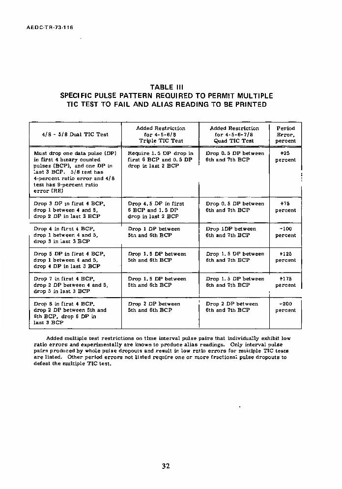
TABLE III SPECIFIC PULSE PATTERN REQUIRED TO PERMIT MULTIPLE
TIC TEST TO FAIL AND ALIAS READING TO BE PRINTED
4/8-5/8 DuaL TIC Test Added Restriction
for 4-5-6/8 Triple TIC Test
Added Restriction for 4-5-6-7/8 Quad TIC Test
Period Error, percent
Must drop one data pulse (DP) in first 4 binary counted pulses (BCP). and one DP in last 3 BCP. 5/8 test has 4-percent ratio error and 4/8 test has 9-percent ratio error (RE)
Require 1.5 DP drop in first 6 BCP and 0. 5 DP drop ir. last 2 BCP
Drop 0. 5 DP between 6th and 7th BCP
+25 percent
■
■
Drop 3 DP in first 4 BCP, drop 1 between 4 and 5, drop 2 DP in last 3 BCP
Drop 4. 5 DP in first 6 BCP and 1.5 DP drop in last 2 BCP
Drop 0. 5 DP between 6th and 7th BCP
+75 percent
Drop 4 in first 4 BCP, drop 1 between 4 and 5, drop 3 in last 3 BCP
Drop 1 DP between 5tn and 6th BCP
Drop 1DP between 6th and 7th BCP
-100 percent
Drop 5 DP in first 4 BCP, drop 1 between 4 and 5, drop 4 DP in last 3 BCP
Drop 1. 5 DP between 5th and 6th BCP
Drop 1. 5 DP between 6th and 7th BCP
+ 125 percent
Drop 7 in first 4 BCP, drop 2 DP between 4 and 5, drop 5 in last 3 BCP
Drop 1. 5 DP between 5th and 6th BCP
Drop 1. 5 DP between 6th and 7th BCP
+175 percent
Drop 8 in first 4 BCP, drop 2 DP between 5th and 6th BCP, drop 6 DP in last 3 BCP
Drop 2 DP between 5th and 6th BCP
Drop 2 DP between 6th and 7th BCP
-r200 percent
Added multiple test restrictions on time interval pulse pairs that individually exhibit low ratio errors and experimentally are known to produce alias readings. Only interval pulse pairs produced by whole pulse dropouts and result ir. low ratio errors for multiple TIC tests are listed. Other period errors not listed require one or more fractional pulse dropouts to defeat the multiple TIC test.
32

AEDC-TR-73-116
APPENDIX III ANALYSIS OF THE DUAL TIME INTERVAL COMPARATOR TEST
The purpose of the dual test is to detect and reject certain alias generating time interval pulse pairs that will pass the 4/8 TIC test or the 5/8 TIC test, but not both. Earlier analysis of the single time in- terval comparator test has been performed by Asher (Ref. 4). The unwanted addition of noise to signal information provides for the gen- eration of pulse patterns other than the periodic pattern produced by the particle traversing the LV probe volume. Consider the waveform shown in Fig. 10. Early triggering on the leading edge of this burst could provide for signal data having a 20 to 1 variation (for a constant noise base) in S/N ratio between the start and the midpoint of the wave- form. For burst signals of short duration (few fringe lines in the probe volume or particle traversing a probe volume corner), it is possible to start and end a sample interval in a low S/N area. It is precisely this signal area that can permit the generation of false or alias readings. To illustrate the mechanism whereby alias readings occur, the follow- ing examples and nomenclature are offered.
Data Pulse Period
LV-Produced Frequency Burst
Positive Edge Triggers Sampling Binaries
jmruwinniuL Resultant Data Pulse Train After Signal Conditioning
The LV-produced frequency burst is converted to a "data pulse" train by band pass filtering and zero crossing detection. The pulse train is now sampled by high-speed binaries responding to the positive edge transitions in the pulse train.
Three time interval pulses are created by the sampling binaries from the data pulse train shown below.
0 2 4 5 6 8
JnjihjTJiiihjiirLTL ^-Data Pulse Train —^ L-Data Pu! Pulse Period Number
33'
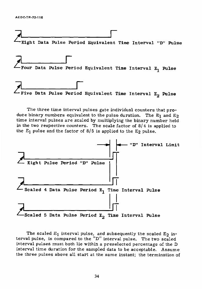
AEDC-TR-73-116
2 r Eight Data Pulse Period Equivalent Time Interval "D" Pulse
2 r Four Data Pulse Period Equivalent Time Interval E, Pulse
2 r Five Data Pulse Period Equivalent Time Interval E2 Pulse
The three time interval pulses gate individual counters that pro- duce binary numbers equivalent to the pulse duration. The Ei and E2 time interval pulses are scaled by multiplying the binary number held in the two respective counters. The scale factor of 8/4 is applied to the Ej pulse and the factor of 8/5 is applied to the E2 pulse.
2 h •D" Interval Limit
Eight Pulse Period "D" Pulse r
2 n Scaled 4 Data Pulse Period E, Time Interval Pulse
? JT Scaled 5 Data Pulse Period E„ Time Interval Pulse
The scaled Ej interval pulse, and subsequently the scaled E2 in- terval pulse, is compared to the "D" interval pulse. The two scaled interval pulses must both lie within a preselected percentage of the D interval time duration for the sampled data to be acceptable. Assume the three pulses above all start at the same instant; the termination of
34

AEDC-TR-73-116
the two scaled pulses must occur within the "D" interval limit "window" or data rejection occurs. The "D" interval limit may be selected to be ±3. 0, 1.5, or 0. 78 percent of the "£)'' interval pulse duration. A trade-off must be made between the selected limit value and the expect- ed data rate since the narrow window discriminates against many "good data'1 frequency bursts. Tnis condition occurs because of the practical limits to period averaging accuracies when sampling short duration pulse trains derived from frequency bursts whose amplitudes randomly vary over a 50 to 1 range.
The scaled time interval pulses used in the example above were employed for illustration only. Such a pulse does not occur within the processor. Rather, the quantized equivalent of the pulse is used in the time interval comparison with the "D" interval pulse. The com- parison is performed within a block of computing circuitry termed the time interval comparator (TIC). A dual comparison is performed: (1) The scaled Ei time interval pulse is compared to the "D" interval pulse; this is referred to as the 4/8 TIC test. (2) The scaled E2 time interval pulse is compared to the "D" interval pulse; this is called the 5/8 TIC test. This terminology will be used in the following discussion.
Consider that in the presence of noise, the frequency burst data may sustain alterations which appear in the resultant data pulse train in the form of data pulse dropout and/or added noise pulses. An ex- ample of the resulting non-periodic pulse train is shown in Fig. Id. The following examples are intended to show how this noise-altered pulse train can produce false or alias readings. Two terms used in these examples, the ratio error and the period error, are defined on page 39.
A data pulse train is shown where a three-pulse dropout occurs in the first half and a two-pulse dropout occurs in the last half of an "cight"-pulse sample interval.
Data Pulses
8 10 12 13
jxmMMhrihhhnhmhhr f t Pulses Actually
Detected by »> Sampling Binaries Data Pulse
Dropout
35

AEDC-TR-73-116
2 f 8 pulse "D" counter actual interval pulse lasts —■» for 13 data pulse periods. Period errpr of ±15 percent of „D1I
reading is ^"^ (100) = 62. 5 percent high Interval Limit o
z r_ n~~ 5 pulse E2 counter actual interval pulse lasts for 8 data pulse periods. The resultant 8 to 5 scaled interval is 98. 5 percent of the "D" interval or a difference of 1. 5 percent exists between the two. This time interval pair will marginally pass the 5/8 TIC test. Experimental data indicate this combination to be one of the most frequent error contributors in single test printed data.
•tit 6 percent
2 r_ vi \-r £— 4 pulse Ej counter actual internal pulse lasts ±1.5 percent "D"
for 7 data pulse periods. The resultant 8 to 4 Interval Limit scaled intervals is 107. 5 percent of the "D" interval or 6 percent greater than the "D" interval limit. Experimental tests show that this interval pair seldom passes the 4/8 TIC test and thus would be effective in the dual test toward rejecting those readings that pass the 5/8 TIC test.
A data pulse train is now shown where a dual pulse dropout occurs in the first half and a dual dropout occurs in the last half.
4^ Data Pulse Periods
6 8 10 ^12
Ji_p_kfLrinh|i|iJi-kmJn_n_ Pulses Counted -1 4 4 5 6 by Sampling I Binaries
36

2 1 n"
AEDC TR-73-116
1.5-percent Limit
8 pulse D counter actual interval pulse lasts for 12 data pulse 12-8
periods. Period error of reading is —-— (100) = 50 percent high.
ÜF D Interval Limit 2 c *— 4 pulse Ej counter actual interval pulse lasts for 6 data pulse
periods. The resultant 8 to 4 scaled interval is exactly 100 percent of the D interval. Experimental tests indicate this combination to be one of the most frequent error contributions in 4/8 single test printed data.
E2 Scaled Interval ±1.5 percent of v D Interval Limit
7 n__\__HV X ~"n r*— 5 percent 5 pulse E2 counter actual interval pulse
lasts for 1 data pulse periods. The resultant 8 to 5 scaled interval is 93. 4 percent of the D interval or 5 percent less than the D interval limit. Experimental tests show that this interval pair seldom passes the 5/8 TIC test and thus would be effective in the dual test toward rejecting those readings that pass the 4/8 TIC test.
In general, the dual test provides similar protection for other in- terval pairs that may pass the 4/8 TIC test or the 5/8 TIC test but not easily both.
An example is given of interval pairs that may pass both individual tests but have additional restrictions imposed when the dual test is performed.
2 4 6 8 10 12 14 16
S]MMMMJ\ß^l4lMMMM^\I\^L 4-Pulse Interval
5-Pulse Interval
37
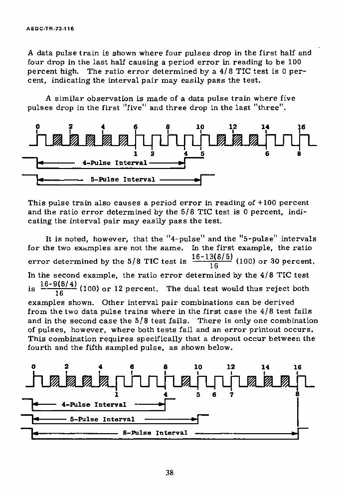
AEDC-TR-73-116
A data pulse train is shown where four pulses drop in the first half and four drop in the last half causing a period error in reading to be 100 percent high. The ratio error determined by a 4/8 TIC test is 0 per- cent, indicating the interval pair may easily pass the test.
A similar observation is made of a data pulse train where five pulses drop in the first "five" and three drop in the last "three".
0 2 4 6 8 10 12 14 16
1 2 A * «a |^ 4-Pulse Interval
5-Pulse Interval
This pulse train also causes a period error in reading of +100 percent and the ratio error determined by the 5/8 TIC test is 0 percent, indi- cating the interval pair may easily pass the test.
It is noted, however, that the "4-pulse" and the "5-pulse" intervals for the two examples are not the same. In the first example, the ratio
•IC_IO/Q/C\
error determined by the 5/8 TIC test is — , . (100) or 30 percent. lb
In the second example, the ratio error determined by the 4/8 TIC test
is — (100) or 12 percent. The dual test would thus reject both lb
examples shown. Other interval pair combinations can be derived from the two data pulse trains where in the first case the 4/8 test fails and in the second case the 5/8 test fails. There is only one combination of pulses, however, where both tests fail and an error printout occurs. This combination requires specifically that a dropout occur between the fourth and the fifth sampled pulse, as shown below.
0 2 4 6 8 10 12 14 16
1 4 5 6 7 p 4-Pulse Interval ^j
Y* 5-Pulse Interval »|
M 8-Pulse Interval
38

AEDC-TR-73-116
In this instance the ratio error for both the 4/8 and the 5/8 test can be shown to be 0 percent. In the experimental data shown in Fig. 2, this condition occurred twice in 1000 samples taken in a low S/N region. The added restriction of a specific pulse pattern imposed by the dual test exists for other interval pairs, as is shown in Table III (Appendix II). The table further shows that additional rejection protection from alias reading print-out could be obtained if a triple TIC test were employed.
In the examples shown above, it was convenient to consider that only integer dropouts occurred. In the very real world of noise/signal mixture, this simple assumption does not hold. The following analyti- cal discussion considers the modification of whole data pulse integer dropouts to include noise-generated added pulses.
Included white noise can cause the following signal modification: (1) a slight shifting or perturbation of a zero crossing position can be caused by small amplitude noise fluctuations; (2) the addition of zero crossings and the deletion of zero crossings can be caused by large amplitude noise.
A computer analysis has been completed which allows for the si- multaneous occurrence of both of these effects via the following gen- eralized equations for (1) the percent ratio error, R, of a time inter- val comparison, and (2) the percent period measurement error, P, as follows:
/(N, -M,- A0+ Aj)N„ \ R<VA,V - 4,;.M;.A;,A;„,; - >) «* <»
/N,-M2-A0+A2 \ /_M A0+AA
",VA2, - ™>( \ - ') - ""{ - ,,• -) Eq. (2)
In Eqs. CD and (2), N\, N2, Mj, and M2 are integers, and -l£ AjS 1 (j = 0, 1, 2). In the sequence of zero crossings generated by signal and noise, it is assumed that the three positive-going zero crossings 0, Ni and N2 (0 < Nj < N2) occur at correspondingly later times (to < tj < t2)> and that these are the critical pulses that gate timing clocks on (0) and off (Nj and N2) for purposes of period measurement and time interval comparison. The time interval tQ to t2 is measured, and time intervals tg to tj and tn to t2 are compared by a ratio test.
39-
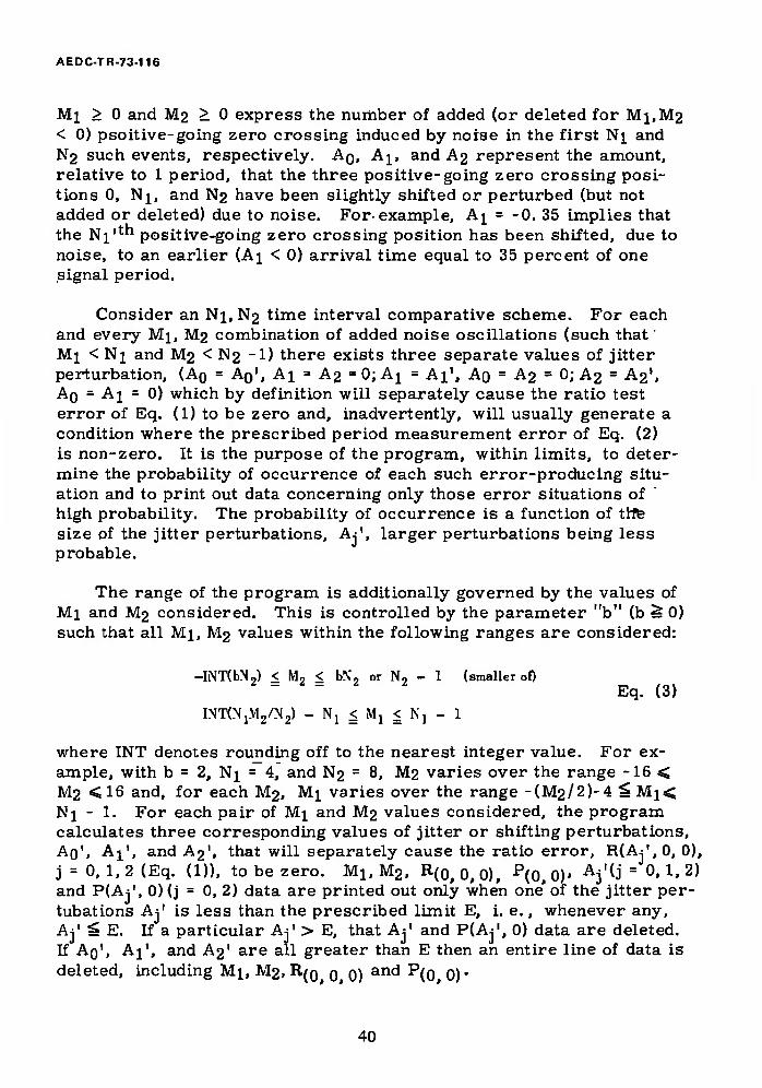
AEDC-TR-73-116
Mi > 0 and M2 > 0 express the number of added (or deleted for Mi,M2 < 0) psoitive-going zero crossing induced by noise in the first Nj and N2 such events, respectively. AQ, AJ, and A2 represent the amount, relative to 1 period, that the three positive-going zero crossing posi- tions 0, Nj, and N2 have been slightly shifted or perturbed (but not added or deleted) due to noise. For example, Aj = -0. 35 implies that the Ni'"1 positive-going zero crossing position has been shifted, due to noise, to an earlier (A\ < 0) arrival time equal to 35 percent of one signal period.
Consider an Nj, N2 time interval comparative scheme. For each and every Mj, M2 combination of added noise oscillations (such that Mi < Ni and M2 < N2 -1) there exists three separate values of jitter perturbation, (AQ = AQ', Al = A2 = 0; Ai = Ai', Ao = A2 = 0; A2 = A2', •^0 = Ai = 0) which by definition will separately cause the ratio test error of Eq. (1) to be zero and, inadvertently, will usually generate a condition where the prescribed period measurement error of Eq. (2) is non-zero. It is the purpose of the program, within limits, to deter- mine the probability of occurrence of each such error-producing situ- ation and to print out data concerning only those error situations of high probability. The probability of occurrence is a function of tlfe size of the jitter perturbations, Aj', larger perturbations being less probable.
The range of the program is additionally governed by the values of Mi and M2 considered. This is controlled by the parameter "b" (b is 0) such that all Mi, M2 values within the following ranges are considered:
-INTtbNn) < M, < bN9 or N, - 1 (smaller o0 2=2=22 Eq. (3)
INT(N,M2/N2) - Nj < Mj < Kj - 1
where INT denotes rounding off to the nearest integer value. For ex- ample, with b = 2, Ni = 4, and N2 = 8, M2 varies over the range -16 < M2 <16 and, for each M2, Mi varies over the range -(M2/2)-4 ^Mi< Ni - 1. For each pair of Mi and M2 values considered, the program calculates three corresponding values of jitter or shifting perturbations, Ao', Ai', and A21, that will separately cause the ratio error, R(Aj',0, 0), j = 0, 1, 2 (Eq. (1)), to be zero. Mi, M2. R(0, 0, 0), p(0, 0)> Aj'<3 = °> *■ 2)
and P(Aj\ 0) (j = 0, 2) data are printed out only when one' of the jitter per- tubations Aj' is less than the prescribed limit E, i. e., whenever any, Aj' ^ E. If a particular Aj' > E, that Aj' and P(Aj', 0) data are deleted. If AQ', AI', and A2' are all greater than E then an entire line of data is deleted, including Mi, M2, R(Q 0 0) and P(0 0)*
40
AEDC-TR-73-116
The program prints out data only for small A^' perturbation amplitudes, | Aj'| < E, where E is an input quantity. If A-j' > E, no data are printed out. If Aj' < E then the following quantities are printed out: M\, M2, P(0j 0) (Eq. (2)), R(0> 0, 0> (Eq. <U), Pj' <j = 0, 1, 2) and Aj' (j = 0, 1, 2). Table I shows typical printed outputs of the program for Nj, N2, and E values of 5, 8, 50 percent and 4, 8, 50 percent. Void places appear- ing in the A^1 and Pj' = PtAj', 0) column indicate that A-;1 > E. Rows are deleted when all Aj'(j = 0, 1. 2) > E. Values of E, P(o, 0)» R(0. 0. 0) and A-;1 are expressed as percentages in the tables.
Considerations which lead to a selection of E are as follows, E S 50 percent allows jitter perturbations of only ±1/2 of one signal period and thereby does not permit the programming and print out of redundant situations. A redundancy occurs when large E can be confused with the addition or loss of signal oscillations. For example, zero ratio error is produced for both (N^ = 5, N2 = 8, Mj = -2, M2 = -2, and Aj = -0. 75) and Nj = 5, N2 = 8, Mj = -1, M2 = -2, and Ai = 0. 25), which are equiv- alent and redundant situations. By restricting E £ 50 percent, redundant situations are eliminated. Small E (e. g. , 0 to 10 percent) permits only small jitter which is usually associated with high S/N, while large E (e. g., 40 to 50 percent) is usually associated with low S/N.
41
UNCLASSIFIED Security Classification
DOCUMENT CONTROL DATA -R&D (Security claaalftcation of litte, body ot abstract and Indexing annotation must be entered whmn the orerall report I» claealllad)
I ORIGINATING * C Ti VI T Y (Corporate author)
Arnold Engineering Development Center Arnold Air Force Station, Tennessee 37389
2«. REPORT SECURITY CLASSIFICATION
UNCLASSIFIED 2b. GROUP
N/A 3 REPORT TITLE
LASER VELOCIMETRY DATA PROCESSING
4 DESCRIPTIVE NOTES (Type ol report and Inclusive datet)
Final Report - 1969 to 1973 s AU THORISl (Flrel name, middle Initial, leal name)
H. T. Kalb, D. B. Brayton, and J. A. McClure, ARO, Inc.
S REPORT DATE
September 1973 7a. TOTAL NO. OF PAGES
47 76. NO. OF REFS
Sa. CONTRACT OR GRANT NO
b. PROJECT NO
e Program Element 65802F
Sa. ORIGINATOR'S REPORT NUMBERIS)
AEDC-TR-73-116
0b. OTHER REPORT NO(3) (Any other number« that may be aeitQned thla report)
AR0-0MD-TR-73-62 10 DISTRIBUTION STATEMENT
Approved for public release; distribution unlimited.
II SUPPLEMENTARY NOTES
Available in DDC
12. SPONSORING MILITARY ACTIVITY
AEDC/AFSC Arnold AFS, Tennessee 37389
13. ABSTRACT
The development of instrumentation for capture and processing of low signal density "frequency burst" data produced by a laser veloci- meter is described. This signal type typically occurs at high flow rates and/or with no artificial seeding. The extension of the instru- ment application into poor signal-to-noise areas is described.
DD FORM 1473 UNCLASSIFIED Security Classification
UNCLASSIFIED Security Classification
KKV WORDS
lasers speed indicators
data processing
density (low)
photomultiplier tubes
UNCLASSIFIED Security Classification