agata global trigger and synchronization...
TRANSCRIPT
Draft version 1.2 – 24 October 2004
M. Bellato – INFN Padova 1
AGATA Global Trigger and Synchronization Hardware
1. Introduction....................................................................................................................................3
2. The Front-end Model.....................................................................................................................4
3. GTS Functionalities .......................................................................................................................7
4. Front-end Simulation.....................................................................................................................9 4.1 Front-end system dead time ................................................................................................................. 9 4.2 The Derandomizer Size........................................................................................................................10 4.3 The Simulation Environment..............................................................................................................11
4.3.1 The carrier.....................................................................................................................................11 4.3.2 The Channel Structure.................................................................................................................13 4.3.3 Trigger Matching..........................................................................................................................14 4.3.4 Simulation Results ........................................................................................................................16
5. Global Timestamp Protocol ........................................................................................................16
6. Global Trigger Algorithms..........................................................................................................16
7. Implementation ............................................................................................................................17 7.1 The root node........................................................................................................................................18 7.2 The backplane.......................................................................................................................................19 7.3 The Fanin-fanout nodes.......................................................................................................................20 7.4 The fibre connections..........................................................................................................................20 7.5 The mezzanine interface ......................................................................................................................21
8. Phase equalization of GTS clocks ...............................................................................................23 8.1 Continuous resets method ...................................................................................................................23
8.1.1 Test results.....................................................................................................................................25 8.2 Direct Measurement.............................................................................................................................28
8.2.2 Test Results....................................................................................................................................28 9. References .....................................................................................................................................29
10. Revision History .........................................................................................................................29
Appendix A. GTS Mezzanine Interface Pin-out ...........................................................................30
Appendix B. Costs ............................................................................................................................31 B.1 Single Crystal prototype costs. ...........................................................................................................31 B.2 Demonstrator costs. .............................................................................................................................31
Draft version 1.2 – 24 October 2004
M. Bellato – INFN Padova 2
Appendix C. Timescale and manpower .........................................................................................33 C.1 GTS interface mezzanine....................................................................................................................33 C.2 Root Node.............................................................................................................................................33 C.3 Fanin-fanout Node...............................................................................................................................33
Draft version 1.2 – 24 October 2004
M. Bellato – INFN Padova 3
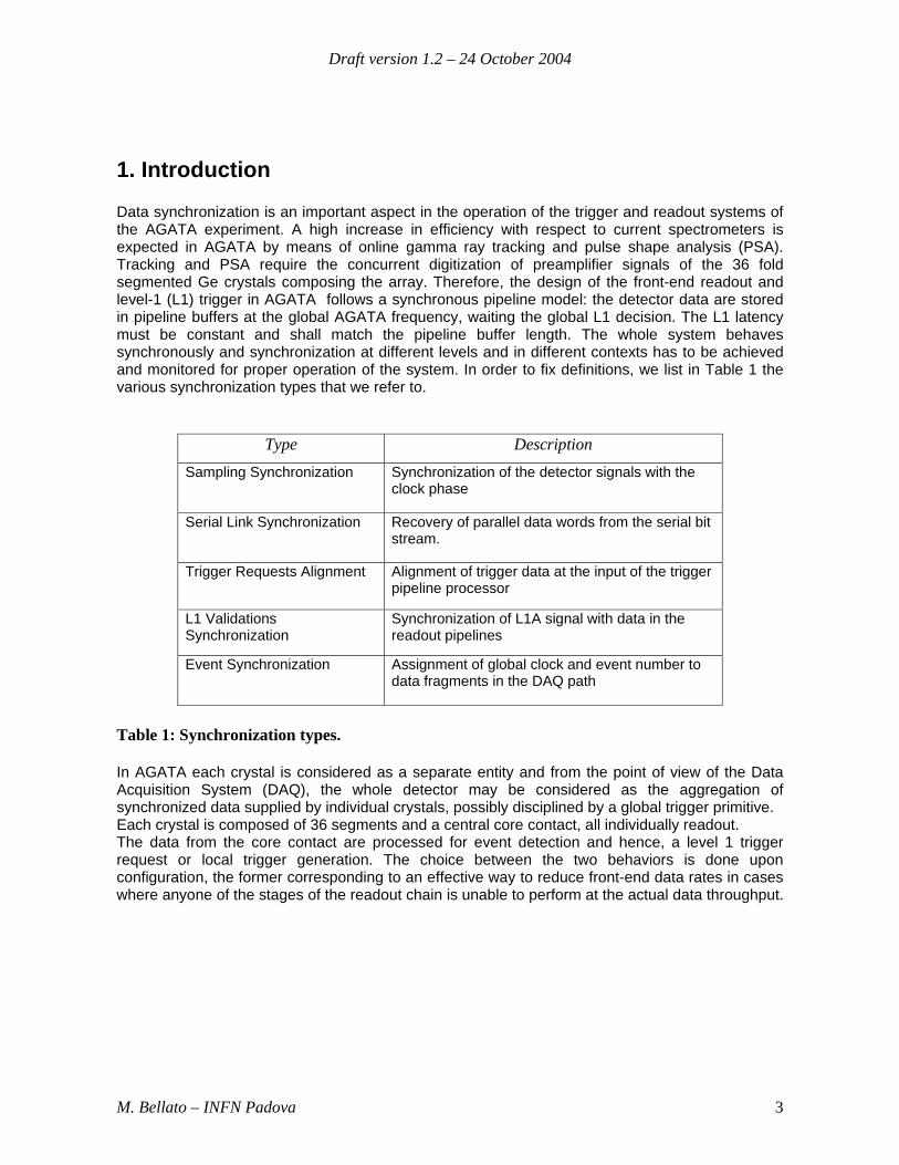
1. Introduction Data synchronization is an important aspect in the operation of the trigger and readout systems of the AGATA experiment. A high increase in efficiency with respect to current spectrometers is expected in AGATA by means of online gamma ray tracking and pulse shape analysis (PSA). Tracking and PSA require the concurrent digitization of preamplifier signals of the 36 fold segmented Ge crystals composing the array. Therefore, the design of the front-end readout and level-1 (L1) trigger in AGATA follows a synchronous pipeline model: the detector data are stored in pipeline buffers at the global AGATA frequency, waiting the global L1 decision. The L1 latency must be constant and shall match the pipeline buffer length. The whole system behaves synchronously and synchronization at different levels and in different contexts has to be achieved and monitored for proper operation of the system. In order to fix definitions, we list in Table 1 the various synchronization types that we refer to.
Type Description
Sampling Synchronization Synchronization of the detector signals with the clock phase
Serial Link Synchronization Recovery of parallel data words from the serial bit stream.
Trigger Requests Alignment Alignment of trigger data at the input of the trigger pipeline processor
L1 Validations Synchronization
Synchronization of L1A signal with data in the readout pipelines
Event Synchronization Assignment of global clock and event number to data fragments in the DAQ path
Table 1: Synchronization types. In AGATA each crystal is considered as a separate entity and from the point of view of the Data Acquisition System (DAQ), the whole detector may be considered as the aggregation of synchronized data supplied by individual crystals, possibly disciplined by a global trigger primitive. Each crystal is composed of 36 segments and a central core contact, all individually readout. The data from the core contact are processed for event detection and hence, a level 1 trigger request or local trigger generation. The choice between the two behaviors is done upon configuration, the former corresponding to an effective way to reduce front-end data rates in cases where anyone of the stages of the readout chain is unable to perform at the actual data throughput.
Draft version 1.2 – 24 October 2004
M. Bellato – INFN Padova 4
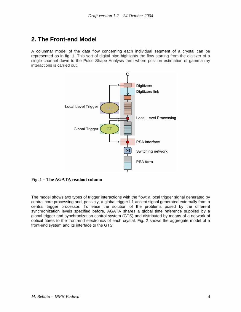
2. The Front-end Model A columnar model of the data flow concerning each individual segment of a crystal can be represented as in fig. 1. This sort of digital pipe highlights the flow starting from the digitizer of a single channel down to the Pulse Shape Analysis farm where position estimation of gamma ray interactions is carried out.
Fig. 1 – The AGATA readout column
The model shows two types of trigger interactions with the flow: a local trigger signal generated by central core processing and, possibly, a global trigger L1 accept signal generated externally from a central trigger processor. To ease the solution of the problems posed by the different synchronization levels specified before, AGATA shares a global time reference supplied by a global trigger and synchronization control system (GTS) and distributed by means of a network of optical fibres to the front-end electronics of each crystal. Fig. 2 shows the aggregate model of a front-end system and its interface to the GTS.
Draft version 1.2 – 24 October 2004
M. Bellato – INFN Padova 5
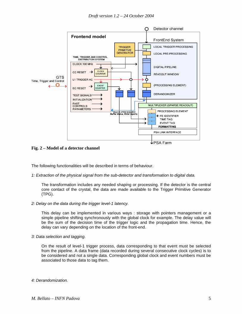
Fig. 2 – Model of a detector channel
The following functionalities will be described in terms of behaviour. 1: Extraction of the physical signal from the sub-detector and transformation to digital data.
The transformation includes any needed shaping or processing. If the detector is the central core contact of the crystal, the data are made available to the Trigger Primitive Generator (TPG).
2: Delay on the data during the trigger level-1 latency.
This delay can be implemented in various ways : storage with pointers management or a simple pipeline shifting synchronously with the global clock for example. The delay value will be the sum of the decision time of the trigger logic and the propagation time. Hence, the delay can vary depending on the location of the front-end.
3: Data selection and tagging.
On the result of level-1 trigger process, data corresponding to that event must be selected from the pipeline. A data frame (data recorded during several consecutive clock cycles) is to be considered and not a single data. Corresponding global clock and event numbers must be associated to those data to tag them.
4: Derandomization.

Draft version 1.2 – 24 October 2004
M. Bellato – INFN Padova 6
Once selected by a level-1 accept, the frame is saved in a multi-event buffer. This buffer stage is needed to allow a frequency derandomization between the level-1 rate and the readout process. The size of the multi-event buffer has to be defined in order to guarantee the smallest buffer-overflow probability possible. A FIFO-like behavior is needed for this buffer.
5: First level merge.
A given number of derandomizer buffers is attached to a merge engine that will readout data associated to a particular event. The engine produces a so called "Front End Event".
6: Front End Event formatting.
The data format of the Front End Event must include the global clock counter and event numbers to allow later data misalignment search [1]. The presence of a Front End identifier could also be required.
7: Transmission to FED
The FE Event is then sent out to the Front-end driver (FED) via a data link. The media and protocol used for this link should be a DAQ standard.
8: Monitoring of the derandomizer filling level
If the readout scheme is such that every derandomizer has the same status at the same time (after readout completion), this case is simple and the solution is straightforward (see below). If the readout scheme is such that every derandomizer can have a different status (e.g. variable event size), warning or worst status must be included to the "Front End Event" for later processing at the FED level.
9: Test facilities To have maximum efficiency in the problem detection, they have to be implemented as high as possible in the readout chain.
10: Processing.
Data processing (e.g. lossless compression) can also be needed in the front end. Location and exact functionality of the processing is to be defined.

Draft version 1.2 – 24 October 2004
M. Bellato – INFN Padova 7
3. GTS Functionalities From the logical description of the front-end operation given above it turns out that a certain number of global time referenced signals are needed. Among them:
1. common clock 2. global clock counter 3. global event counter 4. trigger controls:
i. Throttling of the L1 validation signal ii. Fast commands (fast reset, initialization, etc.) iii. Fast monitoring feedback from the crystals iv. Calibration and test trigger sequence commands v. Monitor of dead time
5. Trigger requests 6. Error reports
In AGATA, the transport medium of all these signals is shared by use of serial optical bidirectional links connecting the front-end electronics of each crystal with a central global trigger and synchronization control unit in a tree-like structure, thus actually merging together the three basic functionalities of synchronization distribution, global control and trigger processing. More in detail: 1: Common clock
This is a 100 MHz digital clock supplied by a central timing unit (possibly GPS disciplined) and used to clock the high speed optical transceivers reaching the front-end electronics of every crystal. At the crystal receiving side the clock is reconstructed and filtered for jitter. The clock signals of each crystal may be equalized for delay and phase, thus accounting for different fibre lengths and different crystal locations in the array.
2: Global clock counter
A 48 bit digital pattern used to tag event fragments before Front-end buffer formatting. The pattern is the actual count of the global clock. It will be used by PSA and global event builders to merge the event fragments in one single event.
3: Global event counter
A 16 bit digital pattern used to tag event fragments before Front-end buffer formatting. The pattern is the actual count of the L1 validations.
4: Trigger controls
The Trigger Control must guarantee that sub-systems are ready to receive every L1 Accept delivered. This is essential to prevent buffers overflows and/or trigger signals missed when the crystals are not ready to receive them. In either case, the consequence would be a loss of synchronization between event fragments.
Draft version 1.2 – 24 October 2004
M. Bellato – INFN Padova 8
Warning signals sent from the crystal through the GTS network, indicating that some of its buffers are almost full, may be received centrally. However this feedback signal can take few microseconds to reach the Trigger Control, which meanwhile could have delivered a number of L1A signals that originate a buffer overflow. This problem is particularly acute in the front-end derandomizers which have a small storage capacity. According to the front-end electronic logical model, the front-end derandomizers after the L1 latency pipelines are the first devices to overflow when the L1A rate is too high. Space and power constraints in the front-ends imply small derandomizer depth and hence these queues are very sensitive to bursty L1A. In general, the derandomizers behave like a first-in-first-out queue: the input/output frequency is directly the L1A rate. The overflow probability is strongly dependent on the ratio between the service time and the buffer depth. The consequence would be of resetting the whole front-end electronics which would cause a severe loss of efficiency in the DAQ. All front-end derandomizers behave identically. Therefore, their occupancy depend only on the L1A rate and on the service time. A state machine receiving the L1A signals can emulate the de-randomizer behavior and determine its occupancy at each new L1A. If a new L1A is estimated to cause a de-randomizer overflow, this L1A is throttled. In general, it would be very difficult to guarantee that the state machine reproduces exactly the buffer status at every time. However in the present case the L1A accept signals are synchronous with the clock and the write and read latencies are measured in multiples of the clock period. It is this time quantization that makes the de-randomizer emulation really possible. A complementary solution to the same problem is to oblige the delivery of L1A signals to comply with a set of trigger rules. These rules take the general form ’no more than n L1A signals in a given time interval’. Suitable rules, inducing a negligible dead time, would minimize the buffer overflow probability.
5: Trigger request
The central core contact signal might be considered as the overlap of all the signals in the segments of a crystal; in fact a deposit of energy in any of the segment will induce a signal in the central core, thus acting as a sort of analog sum of single segment signals. Therefore, the central core can be processed for event localization in a crystal. Suitable algorithms for this task have been identified [] and tested. The outcome of the algorithm may issue a trigger request to the central trigger processor by asserting this signal which is transmitted via the high speed serial links of the GTS network upwards to the central trigger unit. All the trigger requests collected from the crystals at each global clock cycle form a pattern that can be processed centrally for multiplicity or coincidence with ancillary detectors. The result of this processing stage constitutes the L1 validation.
6: Error reports
Abnormal conditions as buffer overflows, local faults, built-in self tests, etc. can be reported centrally for proper corrective actions.
Draft version 1.2 – 24 October 2004
M. Bellato – INFN Padova 9
4. Front-end Simulation The Front End System presents intrinsic inefficiencies by design, in the sense that all level-1 triggers might not be processed. The two major causes of these inefficiencies are the Front End System dead time following a trigger, and the limited size of the Front End Channel derandomizing buffers. For the complete readout chain of AGATA, a maximum acceptable inefficiency has to be defined: a value in the range of a few percents at 1 MHz trigger rate has to be achieved. Unfortunately, this trigger rate is not known as an absolute worst case, hence, to have a good safety margin for system design, we should regard it as the variance of a Gaussian process and take the 6σ value as our absolute worst case.
4.1 Front-end system dead time A dead time is induced after level-1 trigger reception by the hardware architecture of the Local Level Processing electronics. This dead time is due mainly to the time needed to read a frame out of the front-end fifo’s and to the time needed to sink the synchronization tags from the GTS interface mezzanine. As a consequence, triggers occurring during this period cannot be processed, and corresponding event data are lost. An estimation of the inefficiency induced by the Local Level Processing hardware can be calculated with the following assumptions. Let d be the dead time, r the trigger rate. If we consider a Poisson law for the trigger distribution, the probability of one event (at least) occurring during the dead time is:
( ) rderdxeP rdrdl ≈−=⎟⎟
⎠
⎞⎜⎜⎝
⎛−= −− 1
!01
0
assuming that rd is small relative to 1. Hence, at the level of each crystal, 1 microsecond of dead time after local trigger generation will account for 5% of local efficiency loss at 50 KHz trigger rate. Global system inefficiency due to hardware dead time is computed in the following way. Let’s remember how a global trigger is usually generated in AGATA: local triggers generated at the crystal level get routed to a central trigger processor which is configured for asserting a trigger validation whenever a programmable condition is met. The simplest of these conditions is a multiplicity, e.g. pretending that more than one (usually M = [2..30]) trigger requests are asserted in the same time window. It’s easy to realize that, at multiplicity M>1, dead time of one crystal electronics induces a dead time for the whole system. For sake of simplicity, let’s suppose M=2. An event firing crystals, say, no. 1 and 2 gets validated and those crystals enter a 1 microsecond dead time. Any subsequent event firing any two crystals will be validated only if crystals no.1 and 2 are not interested by the new event. The probability of the new event firing crystals no. 1 or 2 is computed by knowing the number of times that crystals no. 1 or 2 are present in all possible combinations without repetition of any two crystals out of 180 (this is the number of HPGe detectors foreseen for AGATA). Let’s take N = the total number of crystals, M = multiplicity: the total number T of combinations without repetition of any M crystals out of N is the well know formula:
( ) ⎟⎟⎠
⎞⎜⎜⎝
⎛−×
=!!
!MNM
NT
Draft version 1.2 – 24 October 2004
M. Bellato – INFN Padova 10
The number of times K that one crystal is present in all possible combinations without repetition of any M crystals out of N is given by :
)!()!1()!1(
MNMN
MNTK
−×−−
=⎟⎟⎟⎟
⎠
⎞
⎜⎜⎜⎜
⎝
⎛
=
So, the probability of the new event firing a crystal that entered a dead time is given by:
NM
TKMPd
2
=×=
It’s to note that, already at multiplicity M=13, with N=180, it’s almost certain that a new event occurring less than one microsecond after the preceding will hit a crystal whose electronics will not catch it…..
4.2 The Derandomizer Size The size allocated to the front-end derandomizing buffers is a crucial issue. On one hand, available space on silicon and power budget lead to minimize the size. On the other hand, data loss probability due to buffer overflow has to be minimized to avoid misalignment in the DAQ, thus inducing large inefficiencies caused by long recovery times. This constraint leads to maximize the derandomizer size. The model used for this study is mainly defined by 3 parameters:
the mean time between two triggers "t", i.e. the inverse of the trigger rate the fifo’s service time "s", i.e. the minimum time between two consecutive read access to
the fifo’s. The fifo depth "d". This parameter is expressed in terms of events (a constant event size is
assumed). With this model, P(n) , the probability of having n events waiting in the fifo is computed. P(n=d), is the probability for the fifo to be full and also the derandomizer inefficiency. To analyze the contribution of these parameters to the global system inefficiency a simulation environment has been setup. We made a faithful description of the Local Level Processing hardware and the GTS interface mezzanine operations by means of the SystemC hardware description language [ ]. Being both synchronous with the GTS distributed global clock, a cycle accurate description of the local trigger generation, GTS handshake mechanism, fifo’s storage and readout and trigger matching procedure has been easy to achieve and deploy.
Draft version 1.2 – 24 October 2004
M. Bellato – INFN Padova 11
4.3 The Simulation Environment
CARRIER
SCC
GTS_IF
ARBITERFAST_MEM
OUT_BUS
CPU
fiber_in (15:0)fiber_in (15:0)
fiber_out (15:0)fiber_out (15:0) timestamp (47:0)timestamp (47:0)
cmd (7:0)cmd (7:0)
L1AL1A
backpressurebackpressure
trigger_ch (13:0)trigger_ch (13:0)
trigger_requesttrigger_request
ch0
(13:
0)ch
0 (1
3:0)
event_num (23:0)event_num (23:0)
ch1
(13:
0)ch
1 (1
3:0)
ch2
(13:
0)ch
2 (1
3:0)
ch3
(13:
0)ch
3 (1
3:0)
bus_
port
bus_
port
Trigger Primitive Generator Frontend System
GTS Interface
rst
rst
rst
rst
trigger_thresh (11:0)trigger_thresh (11:0) local_triggerlocal_triggerhold_time (9:0)hold_time (9:0)
gclk
gclk
gclk
gclk
gclk
gclk
L1A_latency (15:0)L1A_latency (15:0)
matching_window (15:0)matching_window (15:0)
slave_port_Mslave_port_M arbiter_portarbiter_port
spy (15:0)spy (15:0)
ch7
(13:
0)ch
7 (1
3:0)
ch6
(13:
0)ch
6 (1
3:0)
ch5
(13:
0)ch
5 (1
3:0)
ch4
(13:
0)ch
4 (1
3:0)
ch11
(13
:0)
ch11
(13
:0)
ch10
(13
:0)
ch10
(13
:0)
ch9
(13:
0)ch
9 (1
3:0)
ch8
(13:
0)ch
8 (1
3:0)
cpu_portcpu_port
bus_clkbus_clk
bus_clk
bus_clk
bus_clkbus_clk
bus_clk
bus_clk
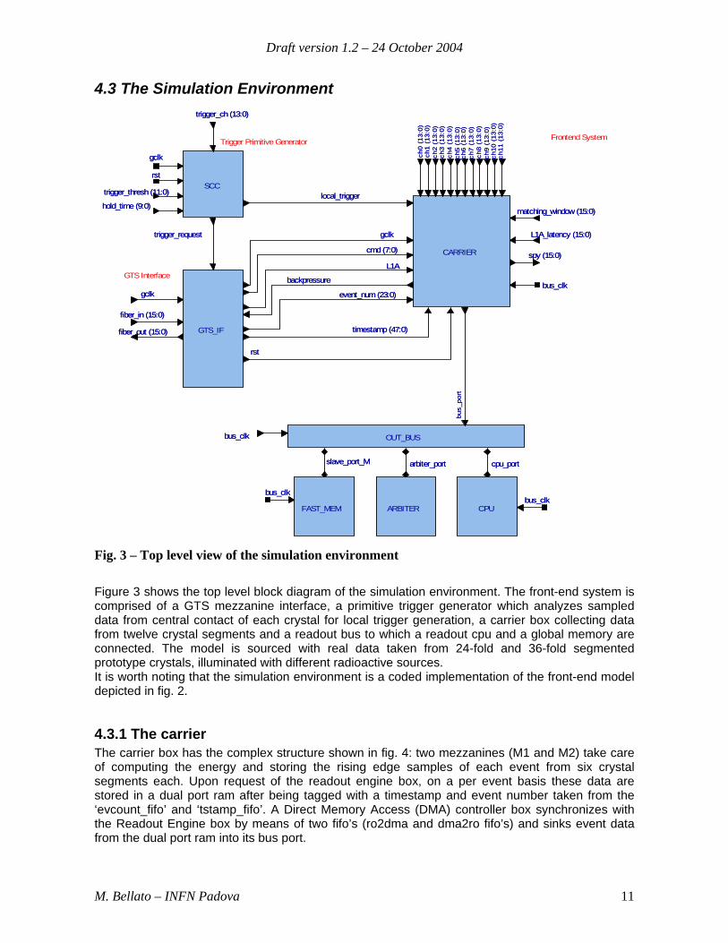
Fig. 3 – Top level view of the simulation environment
Figure 3 shows the top level block diagram of the simulation environment. The front-end system is comprised of a GTS mezzanine interface, a primitive trigger generator which analyzes sampled data from central contact of each crystal for local trigger generation, a carrier box collecting data from twelve crystal segments and a readout bus to which a readout cpu and a global memory are connected. The model is sourced with real data taken from 24-fold and 36-fold segmented prototype crystals, illuminated with different radioactive sources. It is worth noting that the simulation environment is a coded implementation of the front-end model depicted in fig. 2.
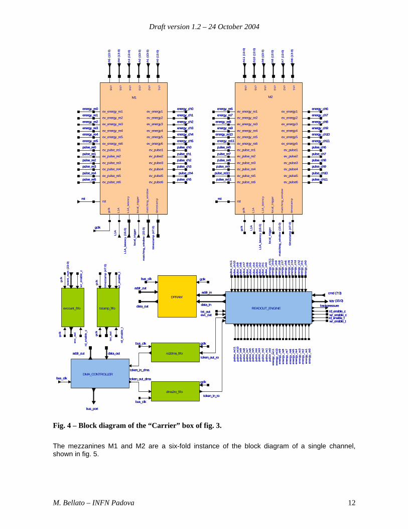
4.3.1 The carrier The carrier box has the complex structure shown in fig. 4: two mezzanines (M1 and M2) take care of computing the energy and storing the rising edge samples of each event from six crystal segments each. Upon request of the readout engine box, on a per event basis these data are stored in a dual port ram after being tagged with a timestamp and event number taken from the ‘evcount_fifo’ and ‘tstamp_fifo’. A Direct Memory Access (DMA) controller box synchronizes with the Readout Engine box by means of two fifo’s (ro2dma and dma2ro fifo’s) and sinks event data from the dual port ram into its bus port.
Draft version 1.2 – 24 October 2004
M. Bellato – INFN Padova 12
ev_energy_re1
ev_energy_re2
ev_energy_re3
ev_energy_re4
ev_energy_re5
ev_energy_re6
ev_pulse_re1
ev_pulse_re2
ev_pulse_re3
ev_pulse_re4
ev_pulse_re5
ev_pulse_re6
ev_energy1
ev_energy2
ev_energy3
ev_energy4
ev_energy5
ev_energy6
ev_pulse1
ev_pulse2
ev_pulse3
ev_pulse4
ev_pulse5
ev_pulse6
ch1
ch2
ch3
ch4
ch5
ch6
gclk
L1A
L1A
_lat
ency
loca
l_tr
igge
r
mat
chin
g_w
indo
w
rst
times
tam
p
M1
ev_energy_re1
ev_energy_re2
ev_energy_re3
ev_energy_re4
ev_energy_re5
ev_energy_re6
ev_pulse_re1
ev_pulse_re2
ev_pulse_re3
ev_pulse_re4
ev_pulse_re5
ev_pulse_re6
ev_energy1
ev_energy2
ev_energy3
ev_energy4
ev_energy5
ev_energy6
ev_pulse1
ev_pulse2
ev_pulse3
ev_pulse4
ev_pulse5
ev_pulse6
ch1
ch2
ch3
ch4
ch5
ch6
gclk
L1A
L1A
_lat
ency
loca
l_tr
igge
r
mat
chin
g_w
indo
w
rst
times
tam
p
M2
tstamp_fifoevcount_fifo
dma2ro_fifo
ro2dma_fifo
DPRAM
READOUT_ENGINE
DMA_CONTROLLER
cmd (7:0)cmd (7:0)
ch1
(13:
0)ch
1 (1
3:0)
ch2
(13:
0)ch
2 (1
3:0)
ch3
(13:
0)ch
3 (1
3:0)
ch0
(13:
0)ch
0 (1
3:0)
bus_portbus_port
backpressurebackpressure
even
t_nu
m (
23:0
)ev
ent_
num
(23
:0)
spy (15:0)spy (15:0)
ch7
(13:
0)ch
7 (1
3:0)
ch6
(13:
0)ch
6 (1
3:0)
ch5
(13:
0)ch
5 (1
3:0)
ch4
(13:
0)ch
4 (1
3:0)
ch11
(13
:0)
ch11
(13
:0)
ch10
(13
:0)
ch10
(13
:0)
ch9
(13:
0)ch
9 (1
3:0)
ch8
(13:
0)ch
8 (1
3:0)
rstrst rstrst
L1A
L1A L1
A
L1A
L1A
_lat
ency
(15
:0)
L1A
_lat
ency
(15
:0)
L1A
_lat
ency
(15
:0)
L1A
_lat
ency
(15
:0)
loca
l_tr
igge
r
loca
l_tr
igge
r
loca
l_tr
igge
r
loca
l_tr
igge
r
mat
chin
g_w
indo
w (
15:0
)
mat
chin
g_w
indo
w (
15:0
)
mat
chin
g_w
indo
w (
15:0
)
mat
chin
g_w
indo
w (
15:0
)
times
tam
p (4
7:0)
times
tam
p (4
7:0)
times
tam
p (4
7:0)
times
tam
p (4
7:0)
times
tam
p (4
7:0)
times
tam
p (4
7:0)
addr_inaddr_in
ener
gy_c
h0
energy_ch0
ener
gy_c
h0
energy_ch0
ener
gy_c
h1
energy_ch1
ener
gy_c
h1
energy_ch1
ener
gy_c
h2
energy_ch2
ener
gy_c
h2
energy_ch2
ener
gy_c
h3
energy_ch3
ener
gy_c
h3
energy_ch3
ener
gy_c
h4
energy_ch4
ener
gy_c
h4
energy_ch4
ener
gy_c
h5
energy_ch5
ener
gy_c
h5
energy_ch5
ener
gy_c
h6
energy_ch6
ener
gy_c
h6
energy_ch6
ener
gy_c
h7
energy_ch7
ener
gy_c
h7
energy_ch7
ener
gy_c
h8
energy_ch8
ener
gy_c
h8
energy_ch8
ener
gy_c
h9
energy_ch9
ener
gy_c
h9
energy_ch9
ener
gy_c
h10
energy_ch10
ener
gy_c
h10
energy_ch10
ener
gy_c
h11
energy_ch11
ener
gy_c
h11
energy_ch11
puls
e_ch
0
pulse_ch0
puls
e_ch
0
pulse_ch0
puls
e_ch
1
pulse_ch1
puls
e_ch
1
pulse_ch1
puls
e_ch
2
pulse_ch2
puls
e_ch
2
pulse_ch2
puls
e_ch
3
pulse_ch3
puls
e_ch
3
pulse_ch3
puls
e_ch
4
pulse_ch4
puls
e_ch
4
pulse_ch4
puls
e_ch
5
pulse_ch5
puls
e_ch
5
pulse_ch5
puls
e_ch
6
pulse_ch6
puls
e_ch
6
pulse_ch6
puls
e_ch
7
pulse_ch7
puls
e_ch
7
pulse_ch7
puls
e_ch
8
pulse_ch8
puls
e_ch
8
pulse_ch8
puls
e_ch
9
pulse_ch9
puls
e_ch
9
pulse_ch9
puls
e_ch
10
pulse_ch10
puls
e_ch
10
pulse_ch10
puls
e_ch
11
pulse_ch11
puls
e_ch
11
pulse_ch11
puls
e_re
10
pulse_re10
puls
e_re
10
pulse_re10
puls
e_re
9
pulse_re9
puls
e_re
9
pulse_re9
puls
e_re
8
pulse_re8
puls
e_re
8
pulse_re8
puls
e_re
7
pulse_re7
puls
e_re
7
pulse_re7
puls
e_re
6
pulse_re6
puls
e_re
6
pulse_re6
puls
e_re
5
pulse_re5
puls
e_re
5
pulse_re5
puls
e_re
4
pulse_re4
puls
e_re
4
pulse_re4
puls
e_re
3
pulse_re3
puls
e_re
3
pulse_re3
puls
e_re
2
pulse_re2
puls
e_re
2
pulse_re2
puls
e_re
1
pulse_re1
puls
e_re
1
pulse_re1
puls
e_re
0
pulse_re0
puls
e_re
0
pulse_re0
ener
gy_r
e11
energy_re11
ener
gy_r
e11
energy_re11
ener
gy_r
e10
energy_re10
ener
gy_r
e10
energy_re10
ener
gy_r
e9
energy_re9
ener
gy_r
e9
energy_re9
ener
gy_r
e8
energy_re8
ener
gy_r
e8
energy_re8
ener
gy_r
e7
energy_re7
ener
gy_r
e7
energy_re7
ener
gy_r
e6
energy_re6
ener
gy_r
e6
energy_re6
ener
gy_r
e5
energy_re5
ener
gy_r
e5
energy_re5
ener
gy_r
e4
energy_re4
ener
gy_r
e4
energy_re4
ener
gy_r
e3
energy_re3
ener
gy_r
e3
energy_re3
ener
gy_r
e2
energy_re2
ener
gy_r
e2
energy_re2
ener
gy_r
e1
energy_re1
ener
gy_r
e1
energy_re1
ener
gy_r
e0
energy_re0
ener
gy_r
e0
energy_re0
puls
e_re
11
pulse_re11
puls
e_re
11
pulse_re11
data_indata_in
token_out_dmatoken_out_dma
token_in_dmatoken_in_dma
addr_out
addr_out
addr_out
addr_out
data_out
data_out
data_out
data_out
token_out_rotoken_out_ro
token_in_rotoken_in_ro
bus_clk
bus_clk
bus_clk
bus_clk
bus_clk
bus_clk
bus_clk
bus_clk
gclk
gclk
gclk
gclk
gclk
gclkgc
lk
gclkgclk
gclk
gclk
gclk
gclk
gclk
gclkgc
lk
gclkgclk
rd_enable_c
rd_e
nabl
e_c
rd_enable_c
rd_e
nabl
e_c
wr_enable_c
wr_
enab
le_c
wr_enable_c
wr_
enab
le_c
rd_enable_t
rd_e
nabl
e_t
rd_enable_t
rd_e
nabl
e_t
wr_enable_t
wr_
enab
le_t
wr_enable_t
wr_
enab
le_t
tst_out
tst_
out
tst_out
tst_
out
evc_out
evc_
out
evc_out
evc_
out
Fig. 4 – Block diagram of the “Carrier” box of fig. 3.
The mezzanines M1 and M2 are a six-fold instance of the block diagram of a single channel, shown in fig. 5.
Draft version 1.2 – 24 October 2004
M. Bellato – INFN Padova 13
channel
ev_energy
ev_pulse
ch
ev_energy_re
ev_pulse_re
gclk
L1A
L1A_latency
local_trigger
matching_window
timestamp
rst
C1
ch1ch1
ev_pulse1ev_pulse1
ev_pulse_re1ev_pulse_re1ev_energy_re1ev_energy_re1
ev_energy1ev_energy1gclkgclk
matching_windowmatching_window
timestamp (15:0)timestamp (15:0)
L1AL1A
L1A_latencyL1A_latency
local_triggerlocal_trigger
rstrst
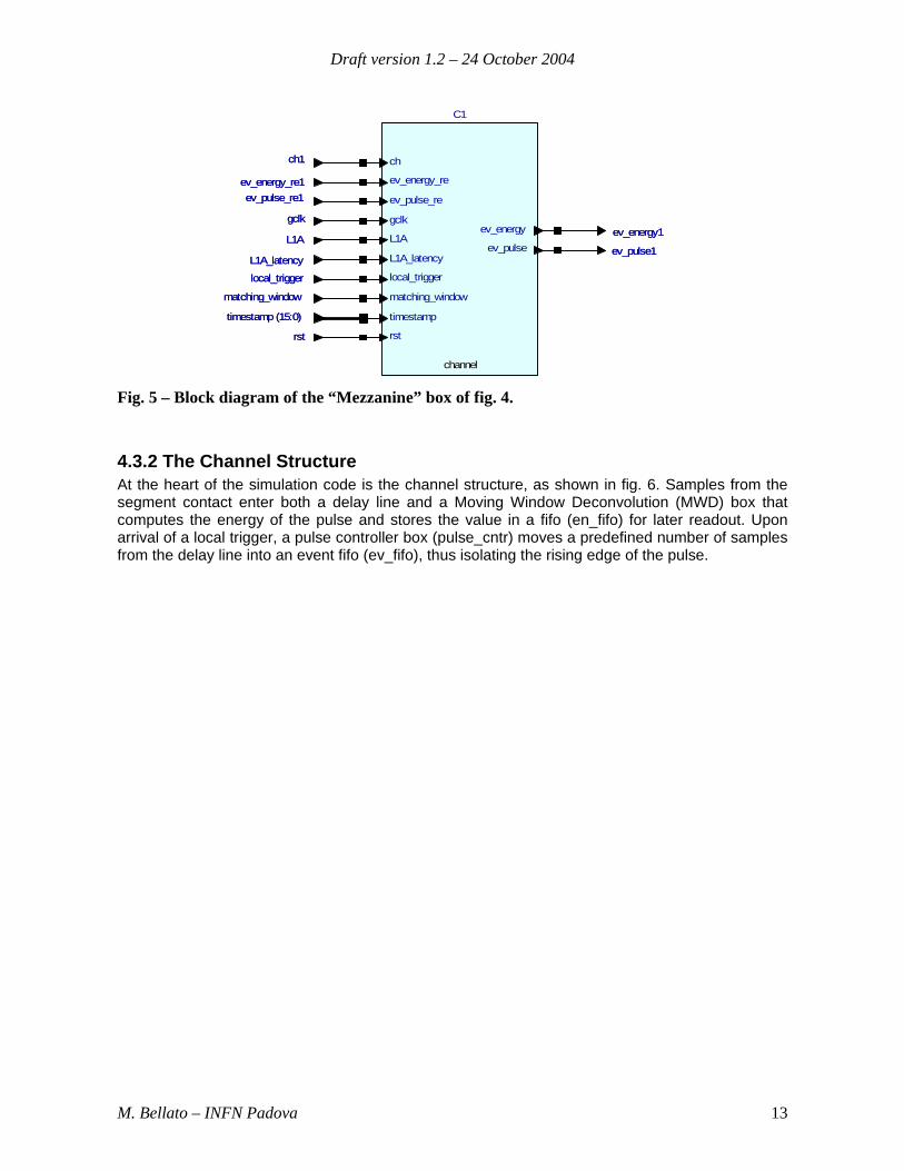
Fig. 5 – Block diagram of the “Mezzanine” box of fig. 4.
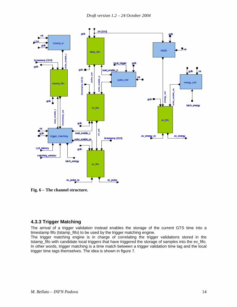
4.3.2 The Channel Structure At the heart of the simulation code is the channel structure, as shown in fig. 6. Samples from the segment contact enter both a delay line and a Moving Window Deconvolution (MWD) box that computes the energy of the pulse and stores the value in a fifo (en_fifo) for later readout. Upon arrival of a local trigger, a pulse controller box (pulse_cntr) moves a predefined number of samples from the delay line into an event fifo (ev_fifo), thus isolating the rising edge of the pulse.
Draft version 1.2 – 24 October 2004
M. Bellato – INFN Padova 14
tstamp_fifo
delay_fifo
ch_fifo
ev_fifo
en_fifo
pulse_cntr
trigger_matching
MWD
energy_cntr
tstamp_in
ch (13:0)ch (13:0)
L1AL1A
writ
e_en
able
_tw
rite_
enab
le_t
puls
e_ou
tpu
lse_
out
times
tam
p_ou
ttim
esta
mp_
out
writ
e_en
able
_pw
rite_
enab
le_p
local_triggerlocal_trigger
read
_ena
ble_
tre
ad_e
nabl
e_t
ener
gy_o
uten
ergy
_out
writ
e_en
able
_en
writ
e_en
able
_en
read_enable_dread_enable_d
read_enable_cread_enable_c
write_enable_evwrite_enable_ev timestamp (15:0)
times
tam
p (1
5:0)
timestamp (15:0)
timestamp (15:0)
times
tam
p (1
5:0)
timestamp (15:0)
ch_o
utch
_out
gclk
gclk
gclk
gclk
gclk
gclkgclk
gclk
gclk
gclk
gclk
gclk
gclk
gclk
gclk
gclk
gclk
gclkgclk
gclk
gclk
gclk
gclk
gclk
ev_pulseev_pulseev_pulse_reev_pulse_re
ev_energyev_energyev_energy_reev_energy_re
L1A_latencyL1A_latency
matching_windowmatching_window
latch_energy
latch_energy
latch_energy
latch_energy
rst
rst
rst
rst
rst
rst
rst
rst
rst
rst
Fig. 6 – The channel structure.
4.3.3 Trigger Matching The arrival of a trigger validation instead enables the storage of the current GTS time into a timestamp fifo (tstamp_fifo) to be used by the trigger matching engine. The trigger matching engine is in charge of correlating the trigger validations stored in the tstamp_fifo with candidate local triggers that have triggered the storage of samples into the ev_fifo. In other words, trigger matching is a time match between a trigger validation time tag and the local trigger time tags themselves. The idea is shown in figure 7.
Draft version 1.2 – 24 October 2004
M. Bellato – INFN Padova 15
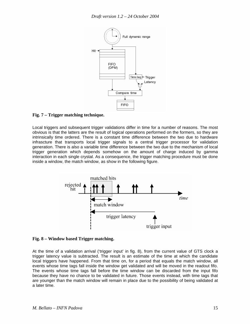
Fig. 7 – Trigger matching technique.
Local triggers and subsequent trigger validations differ in time for a number of reasons. The most obvious is that the latters are the result of logical operations performed on the formers, so they are intrinsically time ordered. There is a constant time difference between the two due to hardware infrascture that transports local trigger signals to a central trigger processor for validation generation. There is also a variable time difference between the two due to the mechanism of local trigger generation which depends somehow on the amount of charge induced by gamma interaction in each single crystal. As a consequence, the trigger matching procedure must be done inside a window, the match window, as show in the following figure.
Fig. 8 – Window based Trigger matching.
At the time of a validation arrival (‘trigger input’ in fig. 8), from the current value of GTS clock a trigger latency value is subtracted. The result is an estimate of the time at which the candidate local triggers have happened. From that time on, for a period that equals the match window, all events whose time tags fall inside the window get validated and will be moved in the readout fifo. The events whose time tags fall before the time window can be discarded from the input fifo because they have no chance to be validated in future. Those events instead, with time tags that are younger than the match window will remain in place due to the possibility of being validated at a later time.
Draft version 1.2 – 24 October 2004
M. Bellato – INFN Padova 16
4.3.4 Simulation Results
5. Global Timestamp Protocol
To be filled …
6. Global Trigger Algorithms
To be filled …
Draft version 1.2 – 24 October 2004
M. Bellato – INFN Padova 17
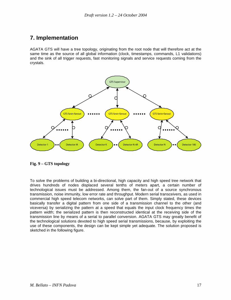
7. Implementation AGATA GTS will have a tree topology, originating from the root node that will therefore act at the same time as the source of all global information (clock, timestamps, commands, L1 validations) and the sink of all trigger requests, fast monitoring signals and service requests coming from the crystals.
Fig. 9 – GTS topology
To solve the problems of building a bi-directional, high capacity and high speed tree network that drives hundreds of nodes displaced several tenths of meters apart, a certain number of technological issues must be addressed. Among them, the fan-out of a source synchronous transmission, noise immunity, low error rate and throughput. Modern serial transceivers, as used in commercial high speed telecom networks, can solve part of them. Simply stated, these devices basically transfer a digital pattern from one side of a transmission channel to the other (and viceversa) by serializing the pattern at a speed that equals the input clock frequency times the pattern width; the serialized pattern is then reconstructed identical at the receiving side of the transmission line by means of a serial to parallel conversion. AGATA GTS may greatly benefit of the technological solutions devoted to high speed serial transmissions, because, by exploiting the use of these components, the design can be kept simple yet adequate. The solution proposed is sketched in the following figure.
Draft version 1.2 – 24 October 2004
M. Bellato – INFN Padova 18
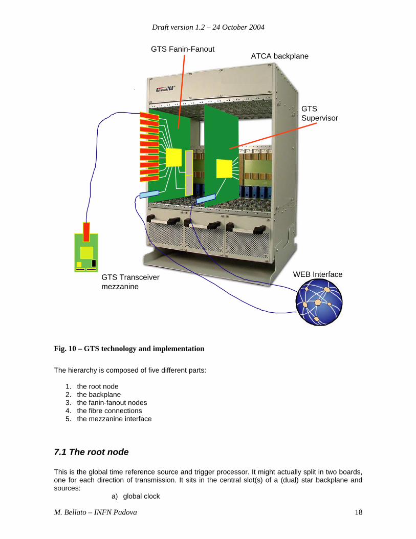
GTSSupervisor
GTS Fanin-Fanout
GTS Transceivermezzanine
WEB Interface
ATCA backplane
Fig. 10 – GTS technology and implementation
The hierarchy is composed of five different parts:
1. the root node 2. the backplane 3. the fanin-fanout nodes 4. the fibre connections 5. the mezzanine interface
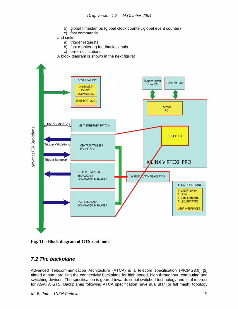
7.1 The root node This is the global time reference source and trigger processor. It might actually split in two boards, one for each direction of transmission. It sits in the central slot(s) of a (dual) star backplane and sources:
a) global clock
Draft version 1.2 – 24 October 2004
M. Bellato – INFN Padova 19
b) global timestamps (global clock counter, global event counter) c) fast commands
and sinks: a) trigger requests b) fast monitoring feedback signals c) error notifications
A block diagram is shown in the next figure:
Fig. 11 – Block diagram of GTS root node
7.2 The backplane Advanced Telecommunication Architecture (ATCA) is a telecom specification (PICMG3.0) [2] aimed at standardizing the connectivity backplane for high speed, high throughput computing and switching devices. The specification is geared towards serial switched technology and is of interest for AGATA GTS. Backplanes following ATCA specification have dual star (or full mesh) topology
Draft version 1.2 – 24 October 2004
M. Bellato – INFN Padova 20
with the two central slots as the centres of the two stars and 6+6 slots on the periphery (14 peripheral slots is also an option). Each slot is connected to the centre by means of a certain number of matched impedance PCB traces (whose differential skew is less than 10ps) and routed to sustain a bit rate in excess of 3 gigabits/s per pair.
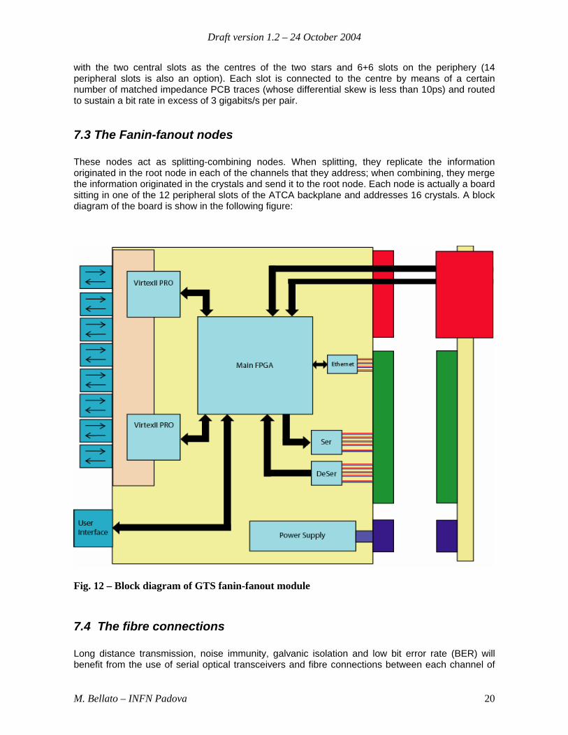
7.3 The Fanin-fanout nodes These nodes act as splitting-combining nodes. When splitting, they replicate the information originated in the root node in each of the channels that they address; when combining, they merge the information originated in the crystals and send it to the root node. Each node is actually a board sitting in one of the 12 peripheral slots of the ATCA backplane and addresses 16 crystals. A block diagram of the board is show in the following figure:
Fig. 12 – Block diagram of GTS fanin-fanout module
7.4 The fibre connections Long distance transmission, noise immunity, galvanic isolation and low bit error rate (BER) will benefit from the use of serial optical transceivers and fibre connections between each channel of
Draft version 1.2 – 24 October 2004
M. Bellato – INFN Padova 21
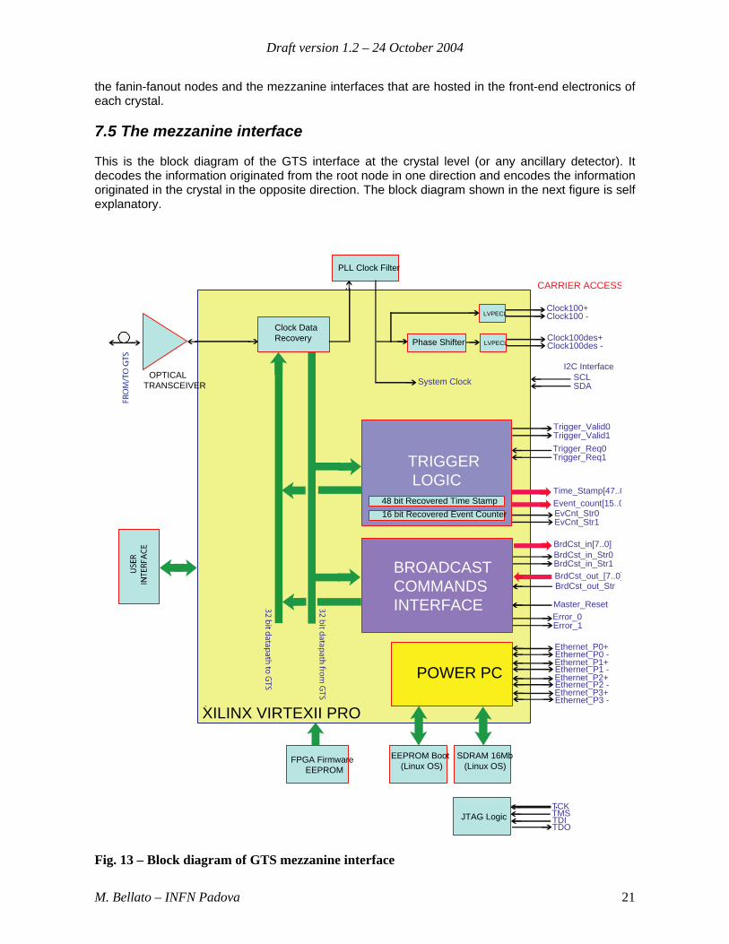
the fanin-fanout nodes and the mezzanine interfaces that are hosted in the front-end electronics of each crystal. 7.5 The mezzanine interface This is the block diagram of the GTS interface at the crystal level (or any ancillary detector). It decodes the information originated from the root node in one direction and encodes the information originated in the crystal in the opposite direction. The block diagram shown in the next figure is self explanatory.
SDRAM 16Mb (Linux OS)
EEPROM Boot (Linux OS)
CARRIER ACCESS
XILINX VIRTEXII PRO
Clock100+Clock100 -
Clock100des+Clock100des -
Trigger_Valid0Trigger_Valid1Trigger_Req0Trigger_Req1
Time_Stamp[47..0Event_count[15..0EvCnt_Str0EvCnt_Str1
BrdCst_in[7..0]BrdCst_in_Str0BrdCst_in_Str1
BrdCst_out_StrBrdCst_out_[7..0]
Ethernet_P0+Ethernet_P0 -Ethernet_P1+Ethernet_P1 -Ethernet_P2+Ethernet_P2 -Ethernet_P3+Ethernet_P3 -
TCKTMSTDITDO
Master_ResetError_0Error_1
Clock DataRecovery Phase Shifter LVPECL
LVPECL
PLL Clock Filter
POWER PC
FPGA Firmware EEPROM
OPTICALTRANSCEIVER
48 bit Recovered Time Stamp16 bit Recovered Event Counter
TRIGGER LOGIC
BROADCASTCOMMANDSINTERFACE
System Clock SCLSDA
I2C Interface
JTAG Logic
Fig. 13 – Block diagram of GTS mezzanine interface
Draft version 1.2 – 24 October 2004
M. Bellato – INFN Padova 22
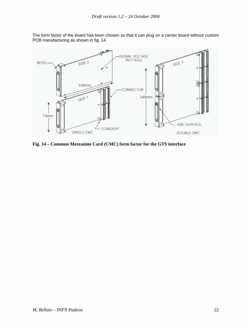
The form factor of the board has been chosen so that it can plug on a carrier board without custom PCB manufacturing as shown in fig. 14
Fig. 14 – Common Mezzanine Card (CMC) form factor for the GTS interface
74mm
149mm
149mm
Draft version 1.2 – 24 October 2004
M. Bellato – INFN Padova 23
8. Phase equalization of GTS clocks The GTS clock, together with its associated timestamp, constitute the time reference for the whole AGATA system. In each crystal, a replica of the main GTS clock, sourced through a dedicated GTS interface mezzanine, feeds the analog-to-digital converters for digitization of segments signals from the charge preamplifiers. The same clock feeds also the communication devices that transfer the relevant information from the crystals up to the local level processing hardware. Moreover, as the whole data acquisition process relies totally on timestamps for the event building process, it is easy to understand that the GTS system must source replicas of its main clock and timestamp that are time aligned at each crystal level. Failing to do so would imply a number of consequences, the most obvious of which is the incorrect time tagging of event fragments and hence incorrect event building, but also potentially incorrect trigger processing. Hence, the problem of clock phase equalization is a crucial issue in AGATA. The reasons behind the misalignment of clock phases among different crystals are multiple. To cite a few there are: different PCB trace lengths, different fiber lengths, different propagation delays of active devices, different routes inside programmable logic devices, different process-voltage-temperature corners of active devices, different equalization fifo’s depths of serializer-deserializer (serdes) devices used throughout the GTS system and many others. While a detailed model of clock phase mismatches is beyond the scope of this document, from what stated above it is obvious that we need to devise a method for diagnose and take care of phase misalignement. An analysis of the problem shows that the contributions to the phase mismatch can be divided in four categories:
Type of Contribution Reason 1 Fixed PCB trace lengths, propagation delays, …
2 Static Equalization fifo’s of serdes devices
3 Slowly changing Temperature, optical phase dispersion, …
4 Rapidly changing Power supply ripple, …
Table 2: Contributions to phase mismatch. While the contributions that fall in the first category can be measured once, those falling in the last three categories must be diagnosed at run-time and fixed with a fast and automated procedure, so that the contribution to the global system inefficiency is negligible. In AGATA, two different methods of phase equalization are currently under investigation:
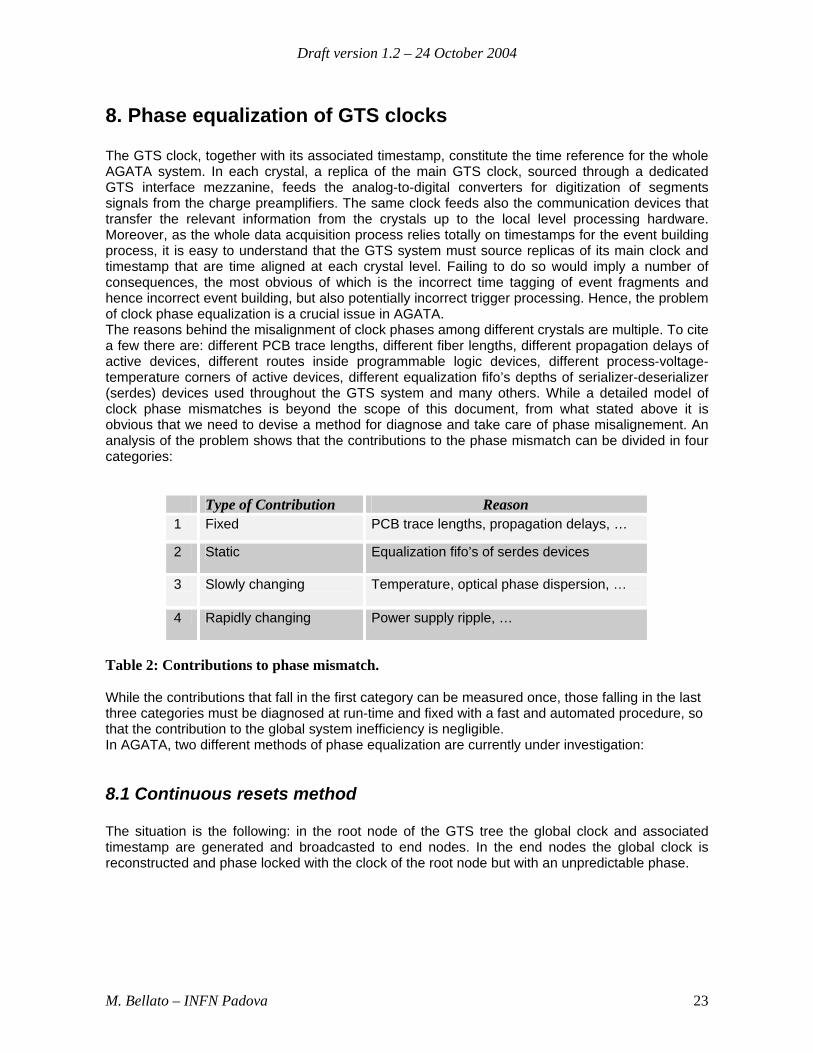
8.1 Continuous resets method The situation is the following: in the root node of the GTS tree the global clock and associated timestamp are generated and broadcasted to end nodes. In the end nodes the global clock is reconstructed and phase locked with the clock of the root node but with an unpredictable phase.
Draft version 1.2 – 24 October 2004
M. Bellato – INFN Padova 24
Fig. 15 – Root node – End node pair with loopback
The main reason of phase uncertainty is contributions of type 2, e.g. due to the nature of clock data recovery circuit (CDR) of serdes devices. By putting a loopback in one end node, from the root node we measure the round trip time of a pulse and try to devise a method from which we can safely assume that the downlink and uplink channels are symmetric and hence the measurement (divided by two) equals the time of flight of a pulse from the root node to that end node. By repeating the measurement for each end node we will know how to setup programmable delay lines at the end nodes in order to reach phase equalization for all crystals. From laboratory test, we can basically assume that the phase of recovered clock at one end node is almost uniformly distributed in one clock period. If we take the phase of recovered clock as a random variable, its probability density function looks like in figure 16 Fig. 16 – Ideal probability density function of recovered clock phase at the end node
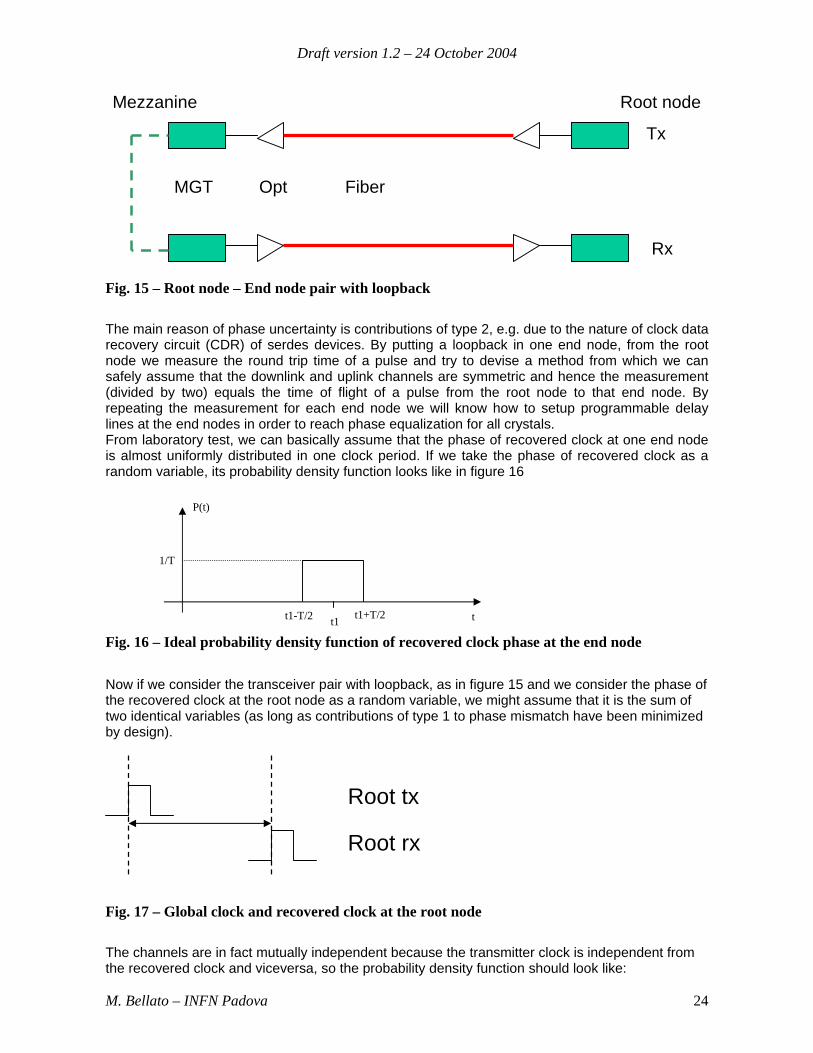
Now if we consider the transceiver pair with loopback, as in figure 15 and we consider the phase of the recovered clock at the root node as a random variable, we might assume that it is the sum of two identical variables (as long as contributions of type 1 to phase mismatch have been minimized by design).
Fig. 17 – Global clock and recovered clock at the root node
The channels are in fact mutually independent because the transmitter clock is independent from the recovered clock and viceversa, so the probability density function should look like:
Root node
MGT Opt Fiber
Mezzanine
Tx
Rx
Root tx
Root rx
t1 t1+T/2 t1-T/2
P(t)
1/T
t
Draft version 1.2 – 24 October 2004
M. Bellato – INFN Padova 25
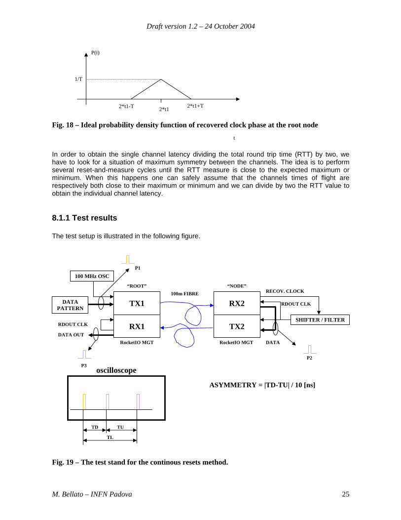
Fig. 18 – Ideal probability density function of recovered clock phase at the root node
In order to obtain the single channel latency dividing the total round trip time (RTT) by two, we have to look for a situation of maximum symmetry between the channels. The idea is to perform several reset-and-measure cycles until the RTT measure is close to the expected maximum or minimum. When this happens one can safely assume that the channels times of flight are respectively both close to their maximum or minimum and we can divide by two the RTT value to obtain the individual channel latency.
8.1.1 Test results The test setup is illustrated in the following figure.
Fig. 19 – The test stand for the continous resets method.
TX1
RX1
RX2
TX2 SHIFTER / FILTER
RECOV. CLOCK
DATA
100m FIBRE
100 MHz OSC
DATA PATTERN
DATA OUT
RDOUT CLK
RDOUT CLK
TD
P1
P3 oscilloscope
RocketIO MGT
“ROOT”
TU
TL
P2
RocketIO MGT
“NODE”
ASYMMETRY = |TD-TU| / 10 [ns]
2*t1 2*t1+T 2*t1-T
P(t)
1/T
t
Draft version 1.2 – 24 October 2004
M. Bellato – INFN Padova 26
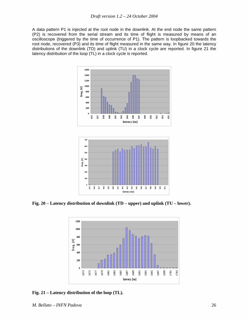
A data pattern P1 is injected at the root node in the downlink. At the end node the same pattern (P2) is recovered from the serial stream and its time of flight is measured by means of an oscilloscope (triggered by the time of occurrence of P1). The pattern is loopbacked towards the root node, recovered (P3) and its time of flight measured in the same way. In figure 20 the latency distributions of the downlink (TD) and uplink (TU) in a clock cycle are reported. In figure 21 the latency distribution of the loop (TL) in a clock cycle is reported.
0
200
400
600
800
1000
1200
1400
1600
835
837
838
840
841
843
844
846
847
849
850
852
853
855
latency [ns]
freq
. [#]
0
100
200
300
400
500
600
700
835
836
837
838
839
840
841
842
843
844
845
846
847
848
849
850
851
latency [ns]
freq
. [#]
Fig. 20 – Latency distribution of downlink (TD – upper) and uplink (TU – lower).
0
200
400
600
800
1000
1200
1673
1675
1677
1679
1681
1683
1685
1687
1689
1691
1693
1695
1697
1699
1701
1703
latency [ns]
freq
. [#]
Fig. 21 – Latency distribution of the loop (TL).
Draft version 1.2 – 24 October 2004
M. Bellato – INFN Padova 27
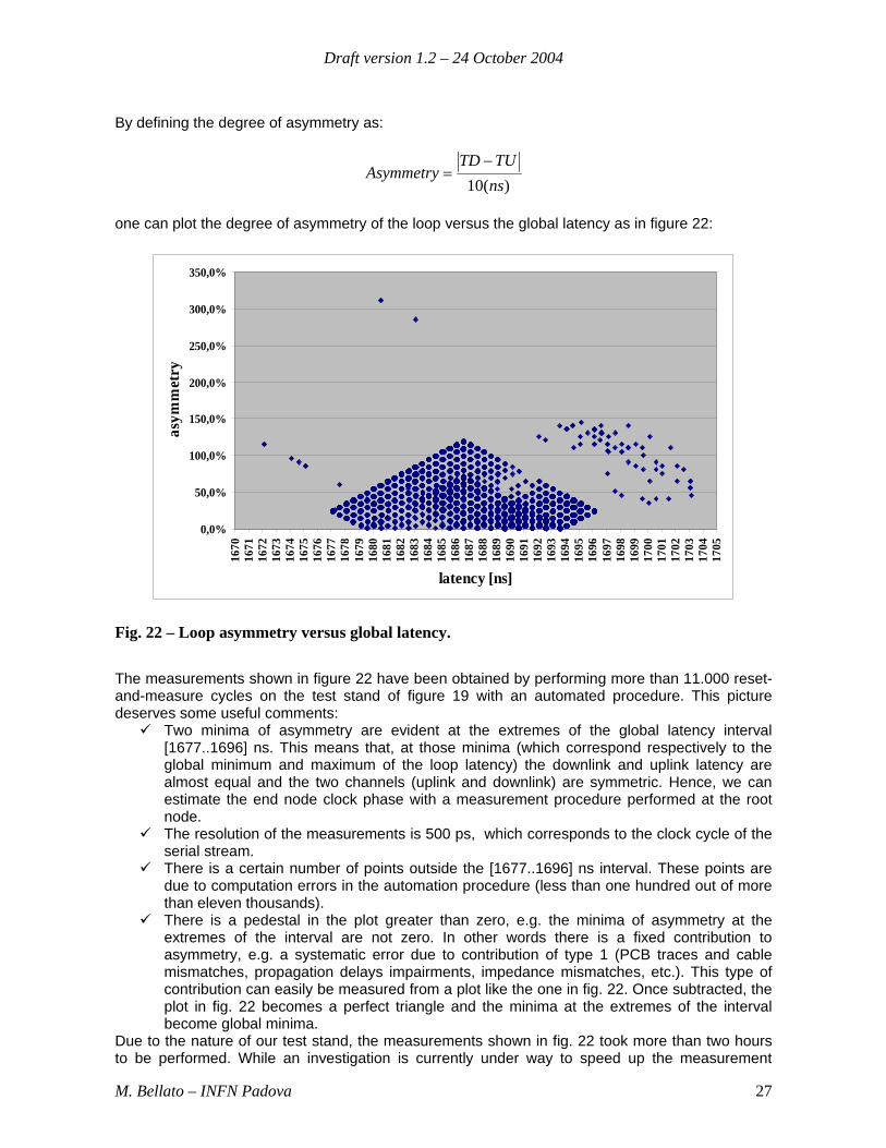
By defining the degree of asymmetry as:
)(10 nsTUTD
Asymmetry−
=
one can plot the degree of asymmetry of the loop versus the global latency as in figure 22:
0,0%
50,0%
100,0%
150,0%
200,0%
250,0%
300,0%
350,0%
1670
1671
1672
1673
1674
1675
1676
1677
1678
1679
1680
1681
1682
1683
1684
1685
1686
1687
1688
1689
1690
1691
1692
1693
1694
1695
1696
1697
1698
1699
1700
1701
1702
1703
1704
1705
latency [ns]
asym
met
ry
Fig. 22 – Loop asymmetry versus global latency.
The measurements shown in figure 22 have been obtained by performing more than 11.000 reset-and-measure cycles on the test stand of figure 19 with an automated procedure. This picture deserves some useful comments:
Two minima of asymmetry are evident at the extremes of the global latency interval [1677..1696] ns. This means that, at those minima (which correspond respectively to the global minimum and maximum of the loop latency) the downlink and uplink latency are almost equal and the two channels (uplink and downlink) are symmetric. Hence, we can estimate the end node clock phase with a measurement procedure performed at the root node.
The resolution of the measurements is 500 ps, which corresponds to the clock cycle of the serial stream.
There is a certain number of points outside the [1677..1696] ns interval. These points are due to computation errors in the automation procedure (less than one hundred out of more than eleven thousands).
There is a pedestal in the plot greater than zero, e.g. the minima of asymmetry at the extremes of the interval are not zero. In other words there is a fixed contribution to asymmetry, e.g. a systematic error due to contribution of type 1 (PCB traces and cable mismatches, propagation delays impairments, impedance mismatches, etc.). This type of contribution can easily be measured from a plot like the one in fig. 22. Once subtracted, the plot in fig. 22 becomes a perfect triangle and the minima at the extremes of the interval become global minima.
Due to the nature of our test stand, the measurements shown in fig. 22 took more than two hours to be performed. While an investigation is currently under way to speed up the measurement

Draft version 1.2 – 24 October 2004
M. Bellato – INFN Padova 28
process, it is evident that it is in the nature of the method itself to perform repetitive resets of serdes devices until a preferred latency is measured. That is, the method can be time consuming because we cannot foresee the time it takes to converge. For this reason it is not obvious that it might be used online, for periodic calibrations of the whole GTS distribution tree at beam time.
8.2 Direct Measurement
8.2.2 Test Results
Draft version 1.2 – 24 October 2004
M. Bellato – INFN Padova 29
9. References [1] – I. Lazarus editor - AGATA Pre-Processing Hardware – Draft. Document – 17/12/2003 [2] – PICMG 3.0 – Advanced Telecommunication Computing Architecture – http://www.picmg.org
10. Revision History 12 Jan 2004 -- Draft version 1.0. 10 Aug 2004 -- Draft version 1.1. 24 Oct 2004 -- Draft version 1.2.
Draft version 1.2 – 24 October 2004
M. Bellato – INFN Padova 30
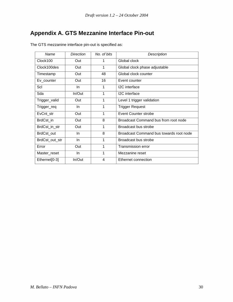
Appendix A. GTS Mezzanine Interface Pin-out The GTS mezzanine interface pin-out is specified as:
Name Direction No. of bits Description
Clock100 Out 1 Global clock
Clock100des Out 1 Global clock phase adjustable
Timestamp Out 48 Global clock counter
Ev_counter Out 16 Event counter
Scl In 1 I2C interface
Sda In/Out 1 I2C interface
Trigger_valid Out 1 Level 1 trigger validation
Trigger_req In 1 Trigger Request
EvCnt_str Out 1 Event Counter strobe
BrdCst_in Out 8 Broadcast Command bus from root node
BrdCst_in_str Out 1 Broadcast bus strobe
BrdCst_out In 8 Broadcast Command bus towards root node
BrdCst_out_str In 1 Broadcast bus strobe
Error Out 1 Transmission error
Master_reset In 1 Mezzanine reset
Ethernet[0-3] In/Out 4 Ethernet connection
Draft version 1.2 – 24 October 2004
M. Bellato – INFN Padova 31
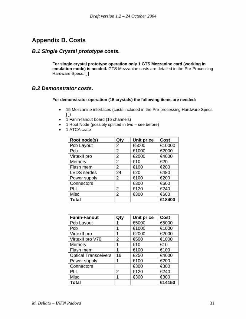
Appendix B. Costs
B.1 Single Crystal prototype costs.
For single crystal prototype operation only 1 GTS Mezzanine card (working in emulation mode) is needed. GTS Mezzanine costs are detailed in the Pre-Processing Hardware Specs. [ ]
B.2 Demonstrator costs.
For demonstrator operation (15 crystals) the following items are needed:
• 15 Mezzanine interfaces (costs included in the Pre-processing Hardware Specs [ ])
• 1 Fanin-fanout board (16 channels) • 1 Root Node (possibly splitted in two – see before) • 1 ATCA crate
Root node(s) Qty Unit price Cost Pcb Layout 2 €5000 €10000 Pcb 2 €1000 €2000 VirtexII pro 2 €2000 €4000 Memory 2 €10 €20 Flash mem 2 €100 €200 LVDS serdes 24 €20 €480 Power supply 2 €100 €200 Connectors €300 €600 PLL 2 €120 €240 Misc 2 €300 €600 Total €18400
Fanin-Fanout Qty Unit price Cost Pcb Layout 1 €5000 €5000 Pcb 1 €1000 €1000 VirtexII pro 1 €2000 €2000 VirtexII pro V70 2 €500 €1000 Memory 1 €10 €10 Flash mem 1 €100 €100 Optical Transceivers 16 €250 €4000 Power supply 1 €100 €200 Connectors €300 €300 PLL 2 €120 €240 Misc 1 €300 €300 Total €14150
Draft version 1.2 – 24 October 2004
M. Bellato – INFN Padova 32
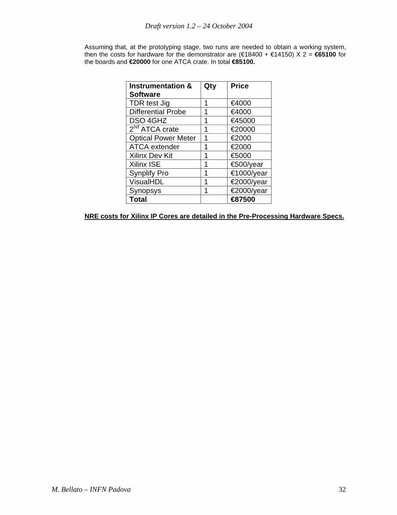
Assuming that, at the prototyping stage, two runs are needed to obtain a working system, then the costs for hardware for the demonstrator are (€18400 + €14150) X 2 = €65100 for the boards and €20000 for one ATCA crate. In total €85100.
Instrumentation & Software
Qty Price
TDR test Jig 1 €4000 Differential Probe 1 €4000 DSO 4GHZ 1 €45000 2nd ATCA crate 1 €20000 Optical Power Meter 1 €2000 ATCA extender 1 €2000 Xilinx Dev Kit 1 €5000 Xilinx ISE 1 €500/year Synplify Pro 1 €1000/yearVisualHDL 1 €2000/yearSynopsys 1 €2000/yearTotal €87500
NRE costs for Xilinx IP Cores are detailed in the Pre-Processing Hardware Specs.
Draft version 1.2 – 24 October 2004
M. Bellato – INFN Padova 33
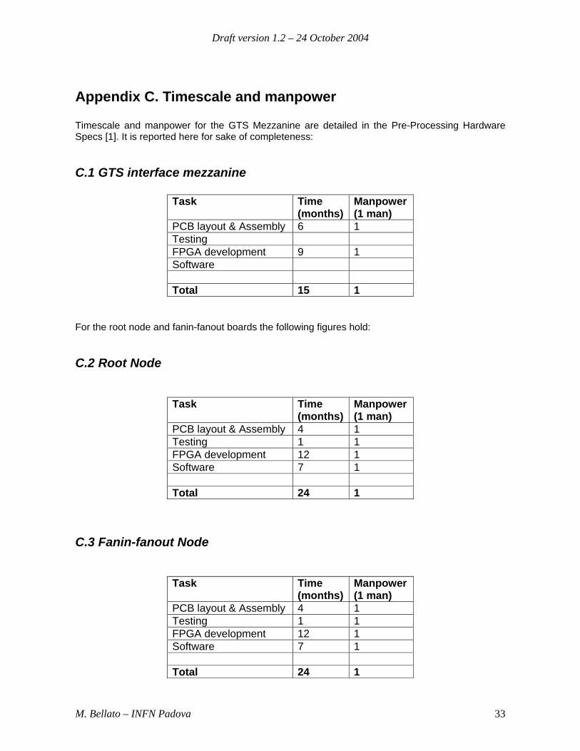
Appendix C. Timescale and manpower Timescale and manpower for the GTS Mezzanine are detailed in the Pre-Processing Hardware Specs [1]. It is reported here for sake of completeness:
C.1 GTS interface mezzanine
Task Time (months)
Manpower (1 man)
PCB layout & Assembly 6 1 Testing FPGA development 9 1 Software Total 15 1
For the root node and fanin-fanout boards the following figures hold:
C.2 Root Node
Task Time (months)
Manpower (1 man)
PCB layout & Assembly 4 1 Testing 1 1 FPGA development 12 1 Software 7 1 Total 24 1
C.3 Fanin-fanout Node
Task Time (months)
Manpower (1 man)
PCB layout & Assembly 4 1 Testing 1 1 FPGA development 12 1 Software 7 1 Total 24 1