agenda -...
TRANSCRIPT

EE141
1
EECS141EECS141Spring 2003Spring 2003
Power Power MinimizationMinimization
Dejan Markovic
Discussion 4Feb 19, 2003
Adapted from “Digital Integrated Circuits2nd Ed”, J.M.Rabaey, A.Chandrakasan, B.Nikolic, © 2003 Prentice Hall/Pearson
AgendaAgenda
Power Dissipation
Circuit Optimization
Technology Scaling
Adapted from “Digital Integrated Circuits2nd Ed”, J.M.Rabaey, A.Chandrakasan, B.Nikolic, © 2003 Prentice Hall/Pearson

EE141
2
Power DissipationPower Dissipation
Adapted from “Digital Integrated Circuits2nd Ed”, J.M.Rabaey, A.Chandrakasan, B.Nikolic, © 2003 Prentice Hall/Pearson
Design for PerformanceDesign for Performance
Keep capacitances smallIncrease transistor sizes
watch out for self-loading!Increase VDD (???)
Adapted from “Digital Integrated Circuits2nd Ed”, J.M.Rabaey, A.Chandrakasan, B.Nikolic, © 2003 Prentice Hall/Pearson
EE141
3
Where Does Power Go in CMOS?Where Does Power Go in CMOS?• Dynamic Power Consumption
• Short Circuit Currents
• Leakage
Charging and Discharging Capacitors
Short Circuit Path between Supply Rails during Switching
Leaking diodes and transistors
Adapted from “Digital Integrated Circuits2nd Ed”, J.M.Rabaey, A.Chandrakasan, B.Nikolic, © 2003 Prentice Hall/Pearson
Dynamic Power DissipationDynamic Power Dissipation
Energy/transition = CL * Vdd2
Power = Energy/transition * f = CL * Vdd2 * f
Need to reduce CL, Vdd, and f to reduce power.
Vin Vout
CL
Vdd
Not a function of transistor sizes!
Adapted from “Digital Integrated Circuits2nd Ed”, J.M.Rabaey, A.Chandrakasan, B.Nikolic, © 2003 Prentice Hall/Pearson

EE141
4
CL
Vdd
Vdd
Vdd -Vt
E0 1→ CL Vdd Vdd Vt–( )••=
Can exploit reduced swing to lower power(e.g., reduced bit-line swing in memory)
Adapted from “Digital Integrated Circuits2nd Ed”, J.M.Rabaey, A.Chandrakasan, B.Nikolic, © 2003 Prentice Hall/Pearson
Circuits with Reduced SwingCircuits with Reduced Swing
Consider switching a CMOS gate for N clock cycles
EN CL Vdd• 2 n N( )•=
n(N): the number of 0->1 transition in N clock cycles
EN : the energy consumed for N clock cycles
Pavg N ∞→lim
ENN-------- fclk•= n N( )
N------------N ∞→
lim C•
LVdd•
2 fclk•=
α0 1→n N( )
N------------N ∞→
lim=
Pavg = α0 1→ C• LVdd• 2 fclk•
Adapted from “Digital Integrated Circuits2nd Ed”, J.M.Rabaey, A.Chandrakasan, B.Nikolic, © 2003 Prentice Hall/Pearson
Node Transition Activity and PowerNode Transition Activity and Power

EE141
5
Short Circuit CurrentsShort Circuit Currents
Vin Vout
CL
Vdd
I VD
D (m
A)
0.15
0.10
0.05
Vin (V)5.04.03.02.01.00.0
Adapted from “Digital Integrated Circuits2nd Ed”, J.M.Rabaey, A.Chandrakasan, B.Nikolic, © 2003 Prentice Hall/Pearson
How to keep ShortHow to keep Short--Circuit Currents Low?Circuit Currents Low?
Short circuit current goes to zero if tfall >> trise,but can’t do this for cascade logic, so ...
Adapted from “Digital Integrated Circuits2nd Ed”, J.M.Rabaey, A.Chandrakasan, B.Nikolic, © 2003 Prentice Hall/Pearson
EE141
6
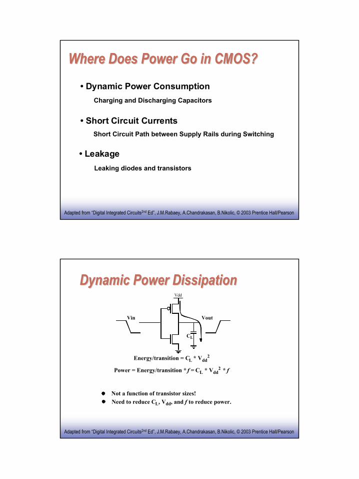
Minimizing ShortMinimizing Short--Circuit PowerCircuit Power
0 1 2 3 4 50
1
2
3
4
5
6
7
8
tsin/tsout
P norm
Vdd =1.5
Vdd =2.5
Vdd =3.3
Adapted from “Digital Integrated Circuits2nd Ed”, J.M.Rabaey, A.Chandrakasan, B.Nikolic, © 2003 Prentice Hall/Pearson
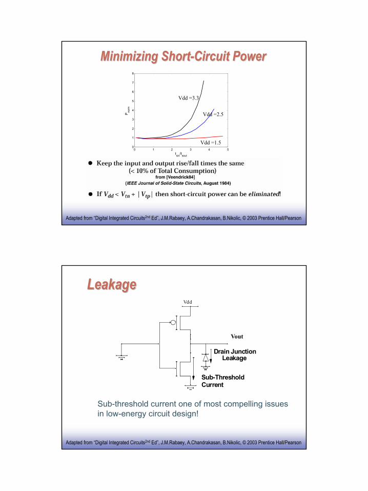
LeakageLeakage
Vout
Vdd
Sub-ThresholdCurrent
Drain JunctionLeakage
Sub-threshold current one of most compelling issuesin low-energy circuit design!
Adapted from “Digital Integrated Circuits2nd Ed”, J.M.Rabaey, A.Chandrakasan, B.Nikolic, © 2003 Prentice Hall/Pearson

EE141
7
ReverseReverse--Biased Diode LeakageBiased Diode Leakage
Np+ p+
Reverse Leakage Current
+
-Vdd
GATE
IDL = JS × A
JS = 10-100 pA/µm2 at 25 deg C for 0.25µm CMOSJS doubles for every 9 deg C!
Adapted from “Digital Integrated Circuits2nd Ed”, J.M.Rabaey, A.Chandrakasan, B.Nikolic, © 2003 Prentice Hall/Pearson
SubthresholdSubthreshold Leakage ComponentLeakage Component
Adapted from “Digital Integrated Circuits2nd Ed”, J.M.Rabaey, A.Chandrakasan, B.Nikolic, © 2003 Prentice Hall/Pearson

EE141
8
Principles for Power ReductionPrinciples for Power ReductionPrime choice: Reduce voltage!
Recent years have seen an acceleration in supply voltage reductionDesign at very low voltages still open question (0.6 … 0.9 V by 2010!)
Reduce switching activityReduce physical capacitance
Device Sizing: for F=20– fopt (energy)=3.53, fopt (performance)=4.47
Adapted from “Digital Integrated Circuits2nd Ed”, J.M.Rabaey, A.Chandrakasan, B.Nikolic, © 2003 Prentice Hall/Pearson
CircuitCircuitOptimizationOptimization
Adapted from “Digital Integrated Circuits2nd Ed”, J.M.Rabaey, A.Chandrakasan, B.Nikolic, © 2003 Prentice Hall/Pearson

EE141
9
♦ Maximize throughput for a given energy
♦ Minimize energy for a given throughput
System Architecture
Micro-Architecture
Logic & Latches
IntroductionIntroduction
Adapted from “Energy-Delay Tradeoffs in Combinational Logic Using Gate Sizing and Supply Voltage Optimization”, V.Stojanovic, D.Markovic, B.Nikolic, M.Horowitz, R.Brodersen, ESSCIRC’02
♦ Boundary curve indicates the best energy-delay tradeoff
♦ Tuning variables• W• Vdd
♦ Interesting problems• number of Vdd’s• utilize W or Vdd
• ↑ or ↓ Vdd for lowest energy
topology A
topology BDelay
Ener
gy
Circuit OptimizationCircuit Optimization
Adapted from “Energy-Delay Tradeoffs in Combinational Logic Using Gate Sizing and Supply Voltage Optimization”, V.Stojanovic, D.Markovic, B.Nikolic, M.Horowitz, R.Brodersen, ESSCIRC’02
EE141
10
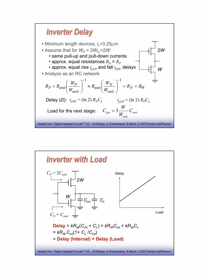
Inverter DelayInverter Delay• Minimum length devices, L=0.25µm• Assume that for WP = 2WN =2W
• same pull-up and pull-down currents• approx. equal resistances RN = RP• approx. equal rise tpLH and fall tpHL delays
• Analyze as an RC network
WNunit
Nunit
unit
PunitP RR
WWR
WWRR ==
≈
=
−− 11
tpHL = (ln 2) RNCL tpLH = (ln 2) RPCLDelay (D):
2W
W
unitunit
gin CWWC 3=Load for the next stage:
Adapted from “Digital Integrated Circuits2nd Ed”, J.M.Rabaey, A.Chandrakasan, B.Nikolic, © 2003 Prentice Hall/Pearson
Inverter with LoadInverter with Load
Load
Delay
Cint CL
Delay = kRW(Cint + CL) = kRWCint + kRWCL
= kRW Cint(1+ CL /Cint)= Delay (Internal) + Delay (Load)
CN = Cunit
CP = 2Cunit
2W
W
Adapted from “Digital Integrated Circuits2nd Ed”, J.M.Rabaey, A.Chandrakasan, B.Nikolic, © 2003 Prentice Hall/Pearson

EE141
11
Delay FormulaDelay Formula
( )
( ) ( )γ/1/1
~
0int ftCCCkRt
CCRDelay
pintLWp
LintW
+=+=
+
Cint = γCgin with γ ≈ 1f = CL/Cgin - effective fanoutR = Runit/W ; Cint =WCunit
tp0 = 0.69RunitCunit
Adapted from “Digital Integrated Circuits2nd Ed”, J.M.Rabaey, A.Chandrakasan, B.Nikolic, © 2003 Prentice Hall/Pearson
Apply to Inverter ChainApply to Inverter Chain
CL
In Out
1 2 N
tp = tp1 + tp2 + …+ tpN
+ +
jgin
jginunitunitpj C
CCRt
,
1,1~γ
LNgin
N
i jgin
jginp
N
jjpp CC
CC
ttt =
+== +
=
+
=∑∑ 1,
1 ,
1,0
1, ,1
γ
Adapted from “Digital Integrated Circuits2nd Ed”, J.M.Rabaey, A.Chandrakasan, B.Nikolic, © 2003 Prentice Hall/Pearson

EE141
12
( ) d
pard dd outp nom
in indd on
WK V W pt g hW W gV V α τ
⋅= ⋅ + = ⋅ ⋅ +
−
♦ Fitting parametersVon, αd, Kd
♦ Effective fanout
effh g h= ⋅
0.5 0.6 0.7 0.8 0.9 1.0 0
0.51.01.5
2.02.53.03.5
Vdd / Vddnom
dela
y in
crea
se
invnand2model
AlphaAlpha--power based Delay Modelpower based Delay Model
Adapted from “Energy-Delay Tradeoffs in Combinational Logic Using Gate Sizing and Supply Voltage Optimization”, V.Stojanovic, D.Markovic, B.Nikolic, M.Horowitz, R.Brodersen, ESSCIRC’02
( ) 2e par out ddE K W W V= ⋅ + ⋅
i i+1
Wwirepnom,i WiWi
( )2 2, 1 , ,i e i dd i nom i dd iec K W V p V−= ⋅ ⋅ + ⋅
,dd iV , 1dd iV +
Wi+1
Wout
Wpar,i
Wi
Siz
ing
Sup
ply
= energy stored on the logic gate i
Switching Component of EnergySwitching Component of Energy
Adapted from “Energy-Delay Tradeoffs in Combinational Logic Using Gate Sizing and Supply Voltage Optimization”, V.Stojanovic, D.Markovic, B.Nikolic, M.Horowitz, R.Brodersen, ESSCIRC’02

EE141
13
♦ Reference/nominal circuit• sized for Dmin @ Vdd
nom
♦ Define delay constraint• Dcon=Dmin(1+dinc/100)
♦ Minimize energy under delay constraint• Vdd scaling (global, discrete, per-stage)• gate sizing• optional buffering
Dmin Delay
Ener
gy
Optimization SetupOptimization Setup
Adapted from “Energy-Delay Tradeoffs in Combinational Logic Using Gate Sizing and Supply Voltage Optimization”, V.Stojanovic, D.Markovic, B.Nikolic, M.Horowitz, R.Brodersen, ESSCIRC’02
♦ Gate Sizing
, , 1
i e i
d eff i eff ii
EW K ec
D K h hW −
∂∂
= − ⋅∂ −
∂
2 1
1
on
dddd
onddd
dd
VE
VV ED VDV V
α
⋅ −∂
∂ = − ⋅∂
− +∂
♦ Supply Voltage
∞ for equal heff
(Dmin)
max at Dmin
Profitability of Optimization Profitability of Optimization Depends on Sensitivity (Depends on Sensitivity (∂∂E/E/∂∂DD))
Adapted from “Energy-Delay Tradeoffs in Combinational Logic Using Gate Sizing and Supply Voltage Optimization”, V.Stojanovic, D.Markovic, B.Nikolic, M.Horowitz, R.Brodersen, ESSCIRC’02
EE141
14
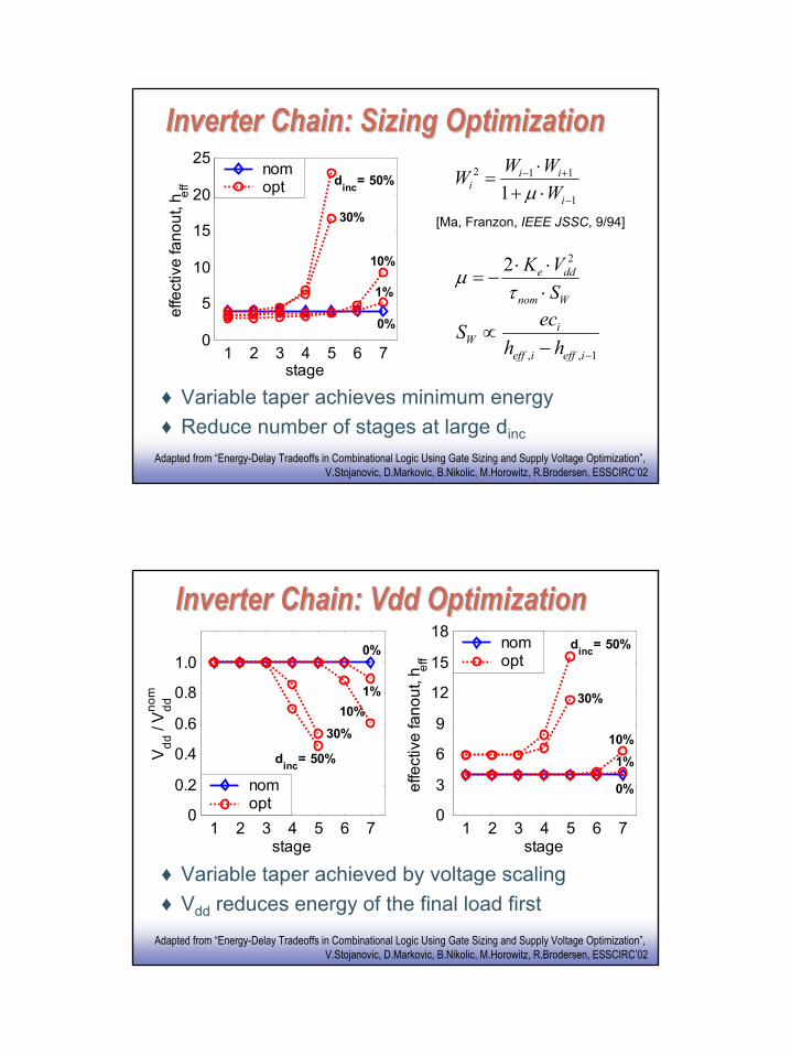
♦ Variable taper achieves minimum energy♦ Reduce number of stages at large dinc
2 1 1
11i i
ii
W WWWµ
− +
−
⋅=
+ ⋅[Ma, Franzon, IEEE JSSC, 9/94]
22 e dd
nom W
K VS
µτ⋅ ⋅
= −⋅
1 2 3 4 5 6 70
5
10
15
20
25
stage
effe
ctiv
e fa
nout
, hef
f
0%
1%
10%
30%
dinc= 50%nomopt
, , 1
iW
eff i eff i
ecSh h −
∝−
Inverter Chain: Sizing OptimizationInverter Chain: Sizing Optimization
Adapted from “Energy-Delay Tradeoffs in Combinational Logic Using Gate Sizing and Supply Voltage Optimization”, V.Stojanovic, D.Markovic, B.Nikolic, M.Horowitz, R.Brodersen, ESSCIRC’02
♦ Variable taper achieved by voltage scaling♦ Vdd reduces energy of the final load first
1 2 3 4 5 6 70
0.2
0.4
0.6
0.8
1.0
stage
Vdd
/ V
ddnom
0%
1%10%
30%
dinc= 50%
nomopt
1 2 3 4 5 6 70
3
6
9
12
15
18
stage
effe
ctiv
e fa
nout
, hef
f
0%
1%10%
30%
dinc= 50%nomopt
Inverter Chain: Vdd OptimizationInverter Chain: Vdd Optimization
Adapted from “Energy-Delay Tradeoffs in Combinational Logic Using Gate Sizing and Supply Voltage Optimization”, V.Stojanovic, D.Markovic, B.Nikolic, M.Horowitz, R.Brodersen, ESSCIRC’02

EE141
15
♦ Parameter with the largest sensitivity has the largest potential for energy reduction
♦ Two discrete supplies mimic per-stage Vdd
0 10 20 30 40 500
20
40
60
80
100
dinc (%)
ener
gy re
duct
ion
(%) cW
gVdd2VddcVdd
0 10 20 30 40 500
0.2
0.4
0.6
0.8
1.0
dinc (%)
Sen
sitiv
ity (n
orm
)
cWgVdd2Vdd
Inverter Chain: Optimization ResultsInverter Chain: Optimization Results
Adapted from “Energy-Delay Tradeoffs in Combinational Logic Using Gate Sizing and Supply Voltage Optimization”, V.Stojanovic, D.Markovic, B.Nikolic, M.Horowitz, R.Brodersen, ESSCIRC’02
∆E = Sens(Vdd)•(-∆D) + Sens(W)•∆D
Delay
Ener
gy/o
p Nominal design
minnomD
( , )nomddf W V
( , )newddf W V
( )ddf V
Joint Optimization: Sizing and VddJoint Optimization: Sizing and Vdd
Adapted from “Methods for True Power Minimization”, R.Brodersen, M.Horowitz, D.Markovic, B.Nikolic, V.Stojanovic, ICCAD’02

EE141
16
♦ Choose a more efficient variable♦ Power vs. reliability limit on Vdd
nom
0 20 40 60 80 1000
20
40
60
80
100
dinc (%)
ener
gy re
duct
ion
(%)
2Vdd + cW2VddgVdd + cWgVddcW
1.0 1.150
10
20
30
40
50
Vdd / Vddnom
ener
gy re
duct
ion
(%) @
Dm
in
Dev
ice
failu
re
42%
67%
Tree Adder: Joint OptimizationTree Adder: Joint Optimization
Adapted from “Energy-Delay Tradeoffs in Combinational Logic Using Gate Sizing and Supply Voltage Optimization”, V.Stojanovic, D.Markovic, B.Nikolic, M.Horowitz, R.Brodersen, ESSCIRC’02
Takeaway PointsTakeaway PointsDesigning for peak performance is VERY power hungry!
Sizing is the most effective for small delay increments while Vdd is better for large delay increments
To reduce energy, it is not always the best to reduce voltage
Adapted from “Energy-Delay Tradeoffs in Combinational Logic Using Gate Sizing and Supply Voltage Optimization”, V.Stojanovic, D.Markovic, B.Nikolic, M.Horowitz, R.Brodersen, ESSCIRC’02

EE141
17
Impact ofImpact ofTechnology Technology ScalingScaling
Adapted from “Digital Integrated Circuits2nd Ed”, J.M.Rabaey, A.Chandrakasan, B.Nikolic, © 2003 Prentice Hall/Pearson
Goals of Technology ScalingGoals of Technology ScalingMake things cheaper:
Want to sell more functions (transistors) per chip for the same moneyBuild same products cheaper, sell the same part for less moneyPrice of a transistor has to be reduced
But also want to be faster, smaller, lower power
Adapted from “Digital Integrated Circuits2nd Ed”, J.M.Rabaey, A.Chandrakasan, B.Nikolic, © 2003 Prentice Hall/Pearson

EE141
18
Technology ScalingTechnology ScalingGoals of scaling the dimensions by 30%:
Reduce gate delay by 30% (increase operating frequency by 43%)Double transistor densityReduce energy per transition by 65% (50% power savings @ 43% increase in frequency
Die size used to increase by 14% per generationTechnology generation spans 2-3 years
Adapted from “Digital Integrated Circuits2nd Ed”, J.M.Rabaey, A.Chandrakasan, B.Nikolic, © 2003 Prentice Hall/Pearson
Technology Evolution (2000 data)Technology Evolution (2000 data)International Technology Roadmap for Semiconductors
18617717116013010690Max µP power [W]1.4
1.2
6-7
1.5-1.8
180
1999
1.7
1.6-1.4
6-7
1.5-1.8
2000
14.9-3.611-37.1-2.53.5-22.1-1.6Max frequency
[GHz],Local-Global
2.52.32.12.42.0Bat. power [W]
109-10987Wiring levels
0.3-0.60.5-0.60.6-0.90.9-1.21.2-1.5Supply [V]
30406090130Technology node [nm]
20142011200820042001Year of Introduction
Node years: 2007/65nm, 2010/45nm, 2013/33nm, 2016/23nm
Adapted from “Digital Integrated Circuits2nd Ed”, J.M.Rabaey, A.Chandrakasan, B.Nikolic, © 2003 Prentice Hall/Pearson
EE141
19
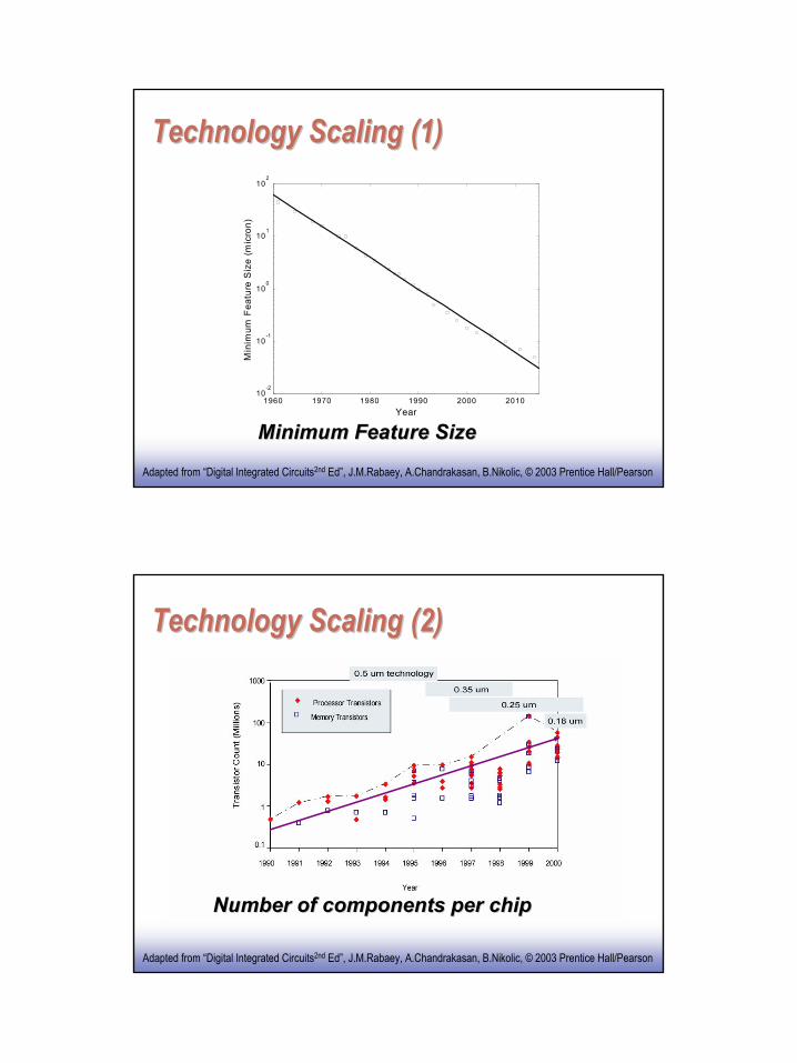
Technology Scaling (1)Technology Scaling (1)
Minimum Feature SizeMinimum Feature Size
1960 1970 1980 1990 2000 201010
-2
10-1
100
101
102
Year
Min
imum
Fea
ture
Siz
e (m
icro
n)
Adapted from “Digital Integrated Circuits2nd Ed”, J.M.Rabaey, A.Chandrakasan, B.Nikolic, © 2003 Prentice Hall/Pearson
Technology Scaling (2) Technology Scaling (2)
Number of components per chipNumber of components per chip
Adapted from “Digital Integrated Circuits2nd Ed”, J.M.Rabaey, A.Chandrakasan, B.Nikolic, © 2003 Prentice Hall/Pearson

EE141
20
Technology Scaling (3)Technology Scaling (3)
Propagation DelayPropagation Delay
Adapted from “Digital Integrated Circuits2nd Ed”, J.M.Rabaey, A.Chandrakasan, B.Nikolic, © 2003 Prentice Hall/Pearson
Technology Scaling Models Technology Scaling Models • Full Scaling (Constant Electrical Field)
• Fixed Voltage Scaling
• General Scaling
ideal model — dimensions and voltage scaletogether by the same factor S
most common model until recently —only dimensions scale, voltages remain constant
most realistic for todays situation —voltages and dimensions scale with different factors
Adapted from “Digital Integrated Circuits2nd Ed”, J.M.Rabaey, A.Chandrakasan, B.Nikolic, © 2003 Prentice Hall/Pearson

EE141
21
Scaling Relationships for Long Channel DevicesScaling Relationships for Long Channel Devices
Adapted from “Digital Integrated Circuits2nd Ed”, J.M.Rabaey, A.Chandrakasan, B.Nikolic, © 2003 Prentice Hall/Pearson
µµProcessorProcessor ScalingScaling
P.Gelsinger: µProcessors for the New Millenium, ISSCC 2001
Adapted from “Digital Integrated Circuits2nd Ed”, J.M.Rabaey, A.Chandrakasan, B.Nikolic, © 2003 Prentice Hall/Pearson
EE141
22
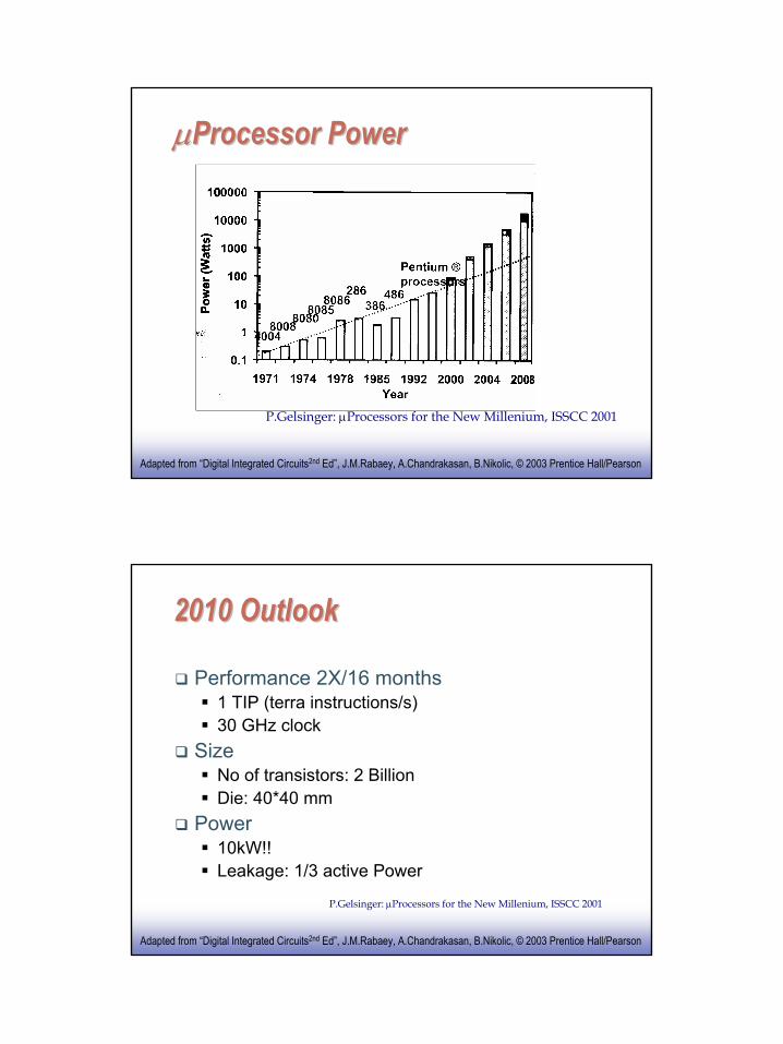
µµProcessorProcessor PowerPower
P.Gelsinger: µProcessors for the New Millenium, ISSCC 2001
Adapted from “Digital Integrated Circuits2nd Ed”, J.M.Rabaey, A.Chandrakasan, B.Nikolic, © 2003 Prentice Hall/Pearson
2010 Outlook2010 Outlook
Performance 2X/16 months1 TIP (terra instructions/s)30 GHz clock
SizeNo of transistors: 2 BillionDie: 40*40 mm
Power10kW!!Leakage: 1/3 active Power
P.Gelsinger: µProcessors for the New Millenium, ISSCC 2001
Adapted from “Digital Integrated Circuits2nd Ed”, J.M.Rabaey, A.Chandrakasan, B.Nikolic, © 2003 Prentice Hall/Pearson

EE141
23
Some interesting questionsSome interesting questions
What will cause this model to break?When will it break?Will the model gradually slow down?
Power and power densityLeakageProcess Variation
Adapted from “Digital Integrated Circuits2nd Ed”, J.M.Rabaey, A.Chandrakasan, B.Nikolic, © 2003 Prentice Hall/Pearson