aif2 programming
TRANSCRIPT

Application Report
Lit. Number – September, 2012
1
AIF2 Programming
Brighton Feng Communication Infrastructure
ABSTRACT
This document is intended to provide some complementary information about the usage of the AIF2. AIF2 examples based on C6670 EVM are introduced.

Overwrite this text with the Lit. Number
2 AIF2 Programming
Contents
1 Introduction .................................................................................................................................. 4 2 AIF2 configuration ....................................................................................................................... 7
2.1 Serdes configuration ............................................................................................................... 7 2.2 AIF2 synchronization configuration ......................................................................................... 9 2.3 DB configuration ................................................................................................................... 14 2.4 PE/PD configuration ............................................................................................................. 15
2.4.1 Bandwidth allocation between channels .................................................................... 15 2.4.2 Radio framing counter configuration .......................................................................... 18 2.4.3 TDD configuration (with packet DMA only) ................................................................ 19
2.5 DIO engines configuration .................................................................................................... 20 2.5.1 DIO configuration for AIF2 Data buffer ...................................................................... 21 2.5.2 DIO configuration for RAC ........................................................................................ 22 2.5.3 DIO configuration for TAC ......................................................................................... 23 2.5.4 DIO configuration for antenna data buffer in DSP memory ........................................ 24
3 Generic packet data over AIF2 .................................................................................................. 26 4 AIF2 debug tips .......................................................................................................................... 27 5 Example Projects ....................................................................................................................... 29
5.1 Packet DMA based example projects ................................................................................... 33 5.2 DIO based example projects ................................................................................................ 37 5.3 To use these example code on other boards ........................................................................ 40
References ......................................................................................................................................... 41
Figures
Figure 1. AIF2 in a LTE baseband solution .................................................................................... 5 Figure 2. AIF2 in a WCDMA baseband solution ............................................................................ 5 Figure 3. AIF2 block diagram ......................................................................................................... 6 Figure 4. AIF2 Serdes configuration .............................................................................................. 8 Figure 5. AIF2 Timer block diagram ............................................................................................... 9 Figure 6. C6670 Antenna Interface Synchronization .................................................................. 10 Figure 7. Synchronization of two DSPs on C6670 EVM .............................................................. 11 Figure 8. Typical delay of AIF2 events ......................................................................................... 12 Figure 9. PE OBSAI Transmission Rules ..................................................................................... 15 Figure 10. Example of Dual Bit Map Rule ...................................................................................... 16 Figure 11. Example of bandwidth equally allocated between channels ...................................... 16 Figure 12. CPRI DBM rules ............................................................................................................. 17 Figure 13. Example of 16 antenna streams pack into 4x CPRI Link ............................................ 17 Figure 14. Radio framing counters ................................................................................................ 18 Figure 15. DIO configuration for AIF2 data buffer ......................................................................... 21 Figure 16. RAC antenna data buffer structure .............................................................................. 22 Figure 17. DIO configuration for RAC ............................................................................................ 23 Figure 18. TAC antenna data buffer structure ............................................................................... 24 Figure 19. DIO configuration for TAC ............................................................................................ 24 Figure 20. DIO configuration for antenna buffer in DSP memory ................................................ 25 Figure 21. AIF2 EE (Error and Exception) Module ........................................................................ 28 Figure 22. AIF connections between two DSPs on C6670 EVM ................................................... 30 Figure 23. Internal loopback test .................................................................................................... 31

Overwrite this text with the Lit. Number
AIF2 Programming 3
Figure 24. External redirection test ................................................................................................ 31 Figure 25. Directory structure of example codes .......................................................................... 32
Tables
Table 1. OBSAI v.s. CPRI ............................................................................................................... 6 Table 2. Number of antenna streams per link .............................................................................. 7 Table 3. Serdes configuration example for different link speed ................................................. 8 Table 4. C6670 AIF2 Synchronization Events .............................................................................. 9 Table 5. Event offset calculation example ................................................................................. 13 Table 6. Event offset calculation example for daisy chain ........................................................ 13 Table 7. Recommended FIFO size for packet DMA channel with different bandwidth ........... 14 Table 8. Utilization of rules for different cases .......................................................................... 16 Table 9. Unit of radio framing counters ...................................................................................... 19 Table 10. DIO configuration parameters ...................................................................................... 20 Table 11. DIO configuration for AIF2 data buffer ......................................................................... 21 Table 12. DIO configuration for RAC ............................................................................................ 22 Table 13. DIO configuration for TAC ............................................................................................ 24 Table 14. DIO configuration for antenna buffer in DSP memory ................................................ 25 Table 15. Generic data transfer in different cases ....................................................................... 26 Table 16. AIF2 common errors and possible resaons ................................................................. 29 Table 17. Source files of the example codes ............................................................................... 32
Overwrite this text with the Lit. Number
4 AIF2 Programming
1 Introduction
The Antenna InterFace version 2 (AIF2) on Keystone DSPs is a peripheral that supports transfers of baseband antenna IQ data between uplink and downlink baseband DSP processors and a high speed SERDES interface. Control data is the secondary data type that is transferred through AIF2 and is nomarlly utilized by the Control & Managment unit of the base station.
The Keystone Communications Infrastructure SoC (System on Chip) is designed to support multiple radio standards including LTE, WCDMA, TD-SCDMA, Wimax, GSM (OBSAI only).
AIF2 is very flexible; it provides a lot of options for customer to configure it. The “KeyStone Architecture Antenna Interface 2 (AIF2) User Guide” describes a lot about AIF configurations. This document is intended to provide some complementary information about the usage of the AIF2.
For WCDMA baseband processing, because of legacy compatibility, the data transfer between AIF2 and RAC (Receiver Accelerator Coprocessor for WCDMA) and TAC (Transmitter Accelerator Coprocessor for WCDMA) use DIO (Direct IO) mode, which is a mode like using the EDMA in the AIF version 1. The DIO engines are optimized for WCDMA processing. DIO requires less memory overhead than the packet DMA and accommodates circular buffering much more favorably than the packet DMA.
For other radio standards, such as LTE and TD-SCDMA, because these standards favor chunk based processing, as opposed to WCDMA which favors streaming, it is recommended to use packet DMA to transfer data between AIF2 and internal processing modules, which is called CPPI (Common Port Programming Interface) mode. The Packet DMA, together with QMSS (Queue Manager SubSystem) are called Multicore Navigator, which control and implement high-speed data packet movement within the DSP, these are new features on Keystone DSPs. These reduce the traditional internal communications load on the DSP core significantly, increasing overall system performance.
Example codes for LTE, WCDMA and TD-SCDMA are provided with this application notes.
The functional block diagrams of a LTE solution and a WCDMA solution with AIF2 is shown in below figures.

Overwrite this text with the Lit. Number
AIF2 Programming 5
Figure 1. AIF2 in a LTE baseband solution
Figure 2. AIF2 in a WCDMA baseband solution
There are 6 AIF2 links on Keystone DSPs, following figure shows the block diagram of AIF2. For more details about the functionality of every module, please refer to Antenna interface user’s guide.

Overwrite this text with the Lit. Number
6 AIF2 Programming
AT
AIF
TimerRP
1/T
RT
VC
VBUSP
(Slave)
RM
RX
MAC
RT
Re-
Transmitter
PE
Protocol
Encoder
SCR
SD
SERDES
TM
TX
MAC
PD
Protocol
Decoder
Serial
RX
Data
Rx
Byte_Clk
AIF2 (Antenna Interface Mega-Module)CI
CPRI
Input
Format
Convert
Serial
TX
Data
CO
CPRI
Output
Format
Convert
AD
AIF2
DMA
Interface
EE
Errors &
Events Events
from all
modules
to and from
all modulesSCR
DB
Data Buffer
FIFOs
CPPI
I/FCPPI
DMA
Sched.CPPI
QM
Rd/Wr
Ra
dio
Sta
nd
ard
Clo
ck
Time
Input
Tx
Byte_Clk
VBUS_Clk
Figure 3. AIF2 block diagram
The AIF2 supports both the OBSAI (Open Base Station Architecture Initiative) and CPRI (Common Public Radio Interface) protocols. Following table compares OBSAI and CPRI.
Table 1. OBSAI v.s. CPRI
OBSAI CPRI
Link rate 2x 1.536Gbps 1.2288Gbps,
4x 3.072Gbps 2.4576Gbps
8x 6.144Gbps 4.9152Gbps
Data precision 8 bits, 16 bits 7 bits, 15 bits (support same number of streams as OBSAI)
8 bits, 16 bits (support less streams than OBSAI)
Packet Efficiency for antenna streams
(16/19)*(399/400)*(20/21)= 0.8
(15/16)= 0.9375
Generally speaking, OBSAI offers more flexibility. For example, when using OBSAI we can configure the DBMRs in conjunction with the modulo rules to provide more flexibility than when using CPRI. With CPRI we only have 1 DBMR per link, and no modulo rules. See section 2.4.1 for more details. But OBSAI has more overhead and requires higher link speed.

Overwrite this text with the Lit. Number
AIF2 Programming 7
CPRI and OBSAI are originally designed for WCDMA, the link rate are tailored to carrier just multiple of WCDMA antenna streams.
Sample rate of TD-SCDMA and typical LTE cases is multiple of WCDMA, so they fit into OBSAI and CPRI very well (Do not really require the feature of DBM (Dual Bit Map)). Following table summarizes number of antenna streams carried by an AIF2 link with typical configuration.
Table 2. Number of antenna streams per link
Radio Standards
Sample
Rate
AxC per Link (Typical case)
2x 4x 8x
TD-SCDMA 1.28MHz 24 48 96
WCDMA 3.84MHz 8 16 32
LTE 5MHz 7.68MHz 4 8 16
LTE 10MHz 15.36MHz 2 4 8
LTE 20MHz 30.72MHz 1 2 4
Please note, total antenna carrier channels support by AIF2 is up to 128 channels per link.
Sample rate of GSM, Wimax or 15MHz LTE is not multiple of WCDMA, DBM (Dual Bit Map) mechanism is required for rate matching.
2 AIF2 configuration
This section provides some complementary information for the configuration of some AIF2 modules.
2.1 Serdes configuration
Serdes need be configured to achieve expected link speed. Following figure shows the relationship between input reference clock and clocks derived from it.

Overwrite this text with the Lit. Number
8 AIF2 Programming
Serdes Macro B4/10
Serdes Macro B8
Serdes PLL
x4, x5, x6 x8, x8.25, x10,
x12 x12.5, x15, x16, x16.5,
x20, x22, x25
Link Rate
8x (x2)
4x (x1)
5x (x1.25)
2x (/2)
OBSAI
3.072GHz
CPRI
2.4576GHz
/10
Dual byte clock
(AIF2 internal system clock)
Link Rate
8x (x2)
4x (x1)
5x (x1.25)
2x (/2)
Link Rate
8x (x2)
4x (x1)
5x (x1.25)
2x (/2)
Link Rate8x (x2)
4x (x1)
5x (x1.25)
2x (/2)
Serdes Tx ClocksAIF2 input
reference clock
0 1
Figure 4. AIF2 Serdes configuration
Input clock are recommended to be between 122.88MHz and 800MHz, the Serdes multiply factor should be setup to generate 3.072GHz internal clock for OBSAI or 2.4576GHz for CPRI. So, the PLL multiply factor should be calculated as:
(PLL multiply factor) = (3.072GHz or 2.4576GHz) / (input clock speed)
The final link speed are derived from the 3.072GHz (for OBSAI) or 2.4576GHz (for CPRI) internal clock according to the link rate configuration. Please note, each link can be configured with different link rate. Following table summarizes the PLL and link rate configuration on TCI6614 EVM with 122.88MHz input clock for AIF2 Serdes.
Table 3. Serdes configuration example for different link speed
Standard PLL x
Link Rate
SerDes Clock Speed
OBSAI 25 8x 122.88*25*2= 6.144Gbps
4x 122.88*25*1= 3.072Gbps
2x 122.88*25/2= 1.536Gbps
CPRI 20 8x 122.88*20*2= 4.9152Gbps
4x 122.88*20*1= 2.4576Gbps
2x 122.88*20/2= 1.2288Gbps
Please note, the dual byte clock (internal clock for TM, AT, PE, PD…) is 307.2MHz for OBSAI or 245.76MHz for CPRI.

Overwrite this text with the Lit. Number
AIF2 Programming 9
2.2 AIF2 synchronization configuration
Antenna data require strict synchronization, in AIF2, the antenna frame synchronization are handled by the AIF2 Timer (AT) module. AIF2 timers run at the AIF2 dual-byte clock (307.2MHz for OBSAI, 245.76MHz for CPRI), and is synchronized to external system frame synchronization signal. Following figure shows the block diagram of AT.
Figure 5. AIF2 Timer block diagram
Basically, PHYT generates events for AIF2 internal timing control, including TM delta, RM Pi, PE1 event and PE2 event. The period of PHYT should be 10ms corresponding to the OBSAI or CPRI frame structure, the offset of these events are programmable with respect to the PHYT frame boundary.
RADT supports various frame size for various radio standards, it generates events mainly for the modules out of AIF2 to facilitate the implementation of different radio standards or different application, and it also generates events to trigger DIO channels to transfer data between AIF2 and other modules. Both period and offset of these events are programmable.
Both the PHYT and RADT must be armed by software and receive sync pulses before they can start counting.
Following table summarize these events generated from AIF2 timers on C6670.
Table 4. C6670 AIF2 Synchronization Events
Events Typical Period
Event 0~7 to DSP cores and EDMA
Frame, Slot or symbol according to application’s requirements
Event 8 for TAC 4 chips

Overwrite this text with the Lit. Number
10 AIF2 Programming
Event 9 for RAC_A
Event 10 for RAC_B
32 chips
6 DIO events for AIF2 4~32 chips
Delta, PE1, PE2 and Pi for AIF2
10ms
Following figure show the block diagram of C6670 antenna interface synchronization.
RP1_SYNC
PHYT_SYNC
RADT_SYNC
EXT_FRAME_EVENT
EDMA
Delta
Clocks
and
Syncs
Derived
from
Same
Clock
Source
TM
PE
AD
RM
Serdes
TACRAC
RAC
Serdes
PE1 Event
PE2 Event
Pi
PHYT
(PHY Timer)
RADT
(Radio Timer)
GEM Core x
RSA for DL
GEM Core x
RSA for DLDSP Core xDSP Core x
Event 9, 10
Event 8
DIO events
Event 0~7
Serdes reference clock
Figure 6. C6670 Antenna Interface Synchronization
To transfer antenna data between two devices, the two devices should be synchronized. Following figure shows the block diagram of the synchronization between two DSPs on C6670 EVM.

Overwrite this text with the Lit. Number
AIF2 Programming 11
TCI6618 EVM
DSP 0Serdes clock
PHYT_SYNC/RADT_SYNC
AIF2
Timer
153.6MHz
Clock
One shot trigger
DSP 1Serdes clock
PHYT_SYNC/RADT_SYNC
AIF2
SW
6
TIMO0
Figure 7. Synchronization of two DSPs on C6670 EVM
On C6670 EVM, the timer output pin TIMO0 of DSP0 can be connected to the single end frame synchronization pins (PHYT_SYNC and RADT_SYNC) of two DSPs through SW6 switch. To run the examples along with this application note, all switches on SW6 should be set to ON state.
In the example, DSP0 timer is configured to generate one shot pulse, which triggers both AIF2 on the DSP0 and DSP1 to run simultaneously. AIF2 timers on both DSP are configured to run freely, external periodical frame synchronization signal is not required for this test. This configuration is for test on EVM only, in a real system, an external periodical Frame synchronization signal should globally trigger AIF2 for keeping synchronization.
Since the basestation is a timing sensitive system, the timing configuration for AIF2 events is very important for AIF to work properly. Blow figure shows the typical delay of the key AIF2 events.

Overwrite this text with the Lit. Number
12 AIF2 Programming
DSP0
Packet DMA
Trigger by first
Sync Frame
boundary
PE
1TM
Delta
PDRM
Pi
TX
SERDES
RX
SERDES
SERDES
DSP1
DB
PE
1
TM
Delta
PDRM
Pi
TX
SERDES
RX
SERDES
SERDESDB
DB -> PE
OBSAI: 28 clocks
CPRI: 0 clocks
PE
2
PE
2
PE1 -> PE2
10 clocks
PE2 -> TM
60 clocks
TM <- PE2
60 clocks
TM->RM including Serdes Delay:
24 clocks for 2x
15 clocks for 4x
10 clocks for 8x
TM->RM including Serdes Delay:
24 clocks for 2x
15 clocks for 4x
10 clocks for 8x
RM -> PE1
100 clocks
DIO triggerred
by DIO eventDMA -> DB
PktDMA (L2): 150+30*channels
PktDMA (DDR): 150+50*channels
DIO (RAC/TAC): 150+10*channels
DIO (L2): 150+30*channels
DIO (DDR): 150+50*channels
DB <- PD <- RM
180 clocks
Figure 8. Typical delay of AIF2 events
The delay values in above figures are typical values that can be used for most cases. The unit of the delay is dual-bye clock.
Please note, the TM->RM delay in above figure does not consider the propagation delay between two devices, this is OK for internal loopback or two devices closely connected in a board. For the connection between two boards or through fiber, additional propagation delay should be added.
For antenna data stream, the packet DMA begins fill DB (Data Buffer) in first frame boundary after TM/RM state machines enter the synchronized state (normally, this will take one frame for loopback test; for real application, it depends on the device on the other end of AIF2 link). So, the antenna data should be pushed into the packet DMA TX queue at least one packet before that frame boundary.
If DIO mode is used, DIO events should be configured properly to trigger the DIO engines to transfer data to/from DB.
Antenna data for all channels should arrive at the DB before PE1 event triggered. The delay for DMA fill DB FIFO depends on number of channels, the more channels, the longer the delay. Additionally, if the DMA of AIF2 competes against other masters for same bus or memory, the delay of DMA may become much longer. Since AIF2 is sensitive to delay, so it is recommended to give the packet DMA of AIF2 highest priority on DSP internal bus system. Smaller DMA delay number can be used if the delay in your application is very deterministic, otherwise, you should use larger number for safe.
Overwrite this text with the Lit. Number
AIF2 Programming 13
The DB will push back to packet DMA when the egress buffer is full, so we do not need worry the packet DMA is start too early than PE.
However, in DIO mode, the DB can not push back to the DIO, so, the DIO can not be started too early, otherwise, the data in the DB will be over written before PE read it. Normally, AIF2 timing events can be setup to make PE start when the egress DB is half-full; ingress DIO starts when the ingress DB is half-full.
Please note, packet data transferred over the OBSAI control messages or CPRI control words always use packet DMA, no matter the antenna data is transferred by DIO or packet DMA. The packet data channel does not like antenna stream channel, the packet DMA begin transfer data packet immediately when the descriptor is pushed into the TX queue. So, packet to the control data channel must be pushed into the TX queue after the first frame boundary after TM/RM state machines enter the synchronized state.
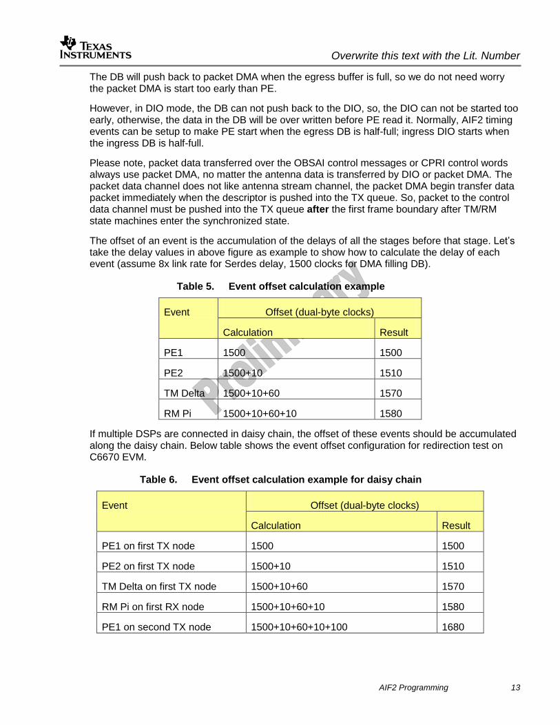
The offset of an event is the accumulation of the delays of all the stages before that stage. Let’s take the delay values in above figure as example to show how to calculate the delay of each event (assume 8x link rate for Serdes delay, 1500 clocks for DMA filling DB).
Table 5. Event offset calculation example
Event Offset (dual-byte clocks)
Calculation Result
PE1 1500 1500
PE2 1500+10 1510
TM Delta 1500+10+60 1570
RM Pi 1500+10+60+10 1580
If multiple DSPs are connected in daisy chain, the offset of these events should be accumulated along the daisy chain. Below table shows the event offset configuration for redirection test on C6670 EVM.
Table 6. Event offset calculation example for daisy chain
Event Offset (dual-byte clocks)
Calculation Result
PE1 on first TX node 1500 1500
PE2 on first TX node 1500+10 1510
TM Delta on first TX node 1500+10+60 1570
RM Pi on first RX node 1500+10+60+10 1580
PE1 on second TX node 1500+10+60+10+100 1680

Overwrite this text with the Lit. Number
14 AIF2 Programming
PE2 on second TX node 1500+10+60+10+100+10 1690
TM Delta on second TX node 1500+10+60+10+100+10+60 1750
RM Pi on second RX node 1500+10+60+10+100+10+60+10 1760
… … …
2.3 DB configuration
The total size of the data buffer RAM for all channels is 16KB for ingress and 16KB for egress, which can be flexible allocated between channels. The FIFO/Buffer for each channel is allocated with following parameters:
Base address. The actual address = 128 * (configured value for this field)
FIFO depth for Packet DMA (each channel can be configured differently). The actual size = 128 << (configured value for this field)
DIO buffer length (128 bytes or 256 bytes, global configuration for all DIO channels)
If only a few channels are used with packet DMA, the FIFO size of these channels may be set as large as possible. Otherwise, the FIFO size of each channel should be configured according to the bandwidth of the channel, following table recommends the minimal FIFO size for different bandwidth of packet DMA channel.
Table 7. Recommended FIFO size for packet DMA channel with different bandwidth
Equivalent Bandwidth of channel Value for FIFO size configuration
Actual FIFO size (Bytes)
8x link (e.g. 80MHz LTE stream) 4 2048
4x link (e.g. 40MHz LTE stream) 3 1024
2x link (e.g. 20MHz LTE stream) 2 512
1x link (e.g. 10MHz LTE stream) 1 256
Less than 1x link bandwidth (e.g. control slot/words of a link)
0 128
Following pseudo code show the configuration for multiple channels.
dbFifoBaseAddress= 0;
for(i=0; i< (number of channels); i++)
{
DbChannel[i].BaseAddress= dbFifoBaseAddress;
DbChannel[i].BufDepth= (FIFO size according to bandwidth of this channel);

Overwrite this text with the Lit. Number
AIF2 Programming 15
dbFifoBaseAddress += (FIFO size);
}
2.4 PE/PD configuration
PE/PD configuration is the relative complicated part of AIF2 configuration. PD/PE was designed to meet different requirements of multiple radio standards. So, for some typical radio standards, the AIF2 seems been over designed, and the configuration for these typical radio standard actually can be simplified.
2.4.1 Bandwidth allocation between channels
AIF2 implements two methods to allocate bandwidth between channels: modulo rules and DBM (Dual Bit Map) rules.
Rules 63
Modulo rule
parameters
DBM rule
parameters
Channel LUT 0
Channel LUT 1
Channel LUT 63
…...
mod
ctl_msg
index
link
dbm_x
Bit map 1
Bit map 2
dbm_1mult
dbm_1size
dbm_2size
Rules 1
Modulo rule
parameters
DBM rule
parameters
Channel LUT 0
Channel LUT 1
Channel LUT 63
…...
mod
ctl_msg
index
link
dbm_x
Bit map 1
Bit map 2
dbm_1mult
dbm_1size
dbm_2size
64x
Frame
FSM
Rules 0
Modulo rule
parameters
DBM rule
parameters
Channel LUT 0
Channel LUT 1
Channel LUT 63
…...
mod
ctl_msg
index
link
dbm_x
Bit map 1
Bit map 2
dbm_1mult
dbm_1size
dbm_2size
Figure 9. PE OBSAI Transmission Rules
Module rules can allocate bandwidth equally between channels. To use this method solely, it requires that available link bandwidth is multiple of the bandwidth for an individual antenna carrier channel; this is the case for some radio stream channels, such as WCDMA, TD-SCDMA and LTE (5MHz, 10MHz, 20MHz). Refer to Table 2 for more information.
DBM rules can also allocate bandwidth equally between channels. The real enhancement of DBM rules is to support radio stream, such as GSM, Wimax, or 15MHz LTE, the available link bandwidth is not multiple of these radio stream channels. The DBM rules actually implement rate matching by insert some dummy data (called “bubble”).
For example, if (available link bandwidth)/(antenna stream bandwidth) = 10/3= 3.33333…
Following figure shows how the 3 antenna streams fit into the AIF2 link with DBM rules.
Bubb
le
AxC
1
AxC
3
AxC
2
AxC
1
AxC
3
AxC
2
AxC
1
AxC
3
AxC
2
AxC
1
AxC
3
AxC
2
AxC
1
AxC
3
AxC
2
AxC
1
AxC
3
AxC
2
Bubb
le
One message group

Overwrite this text with the Lit. Number
16 AIF2 Programming
Figure 10. Example of Dual Bit Map Rule
For above example, the key DBM configuration is: X=3, bit map= 001, bit map size =3
On the other hand, if the link bandwidth is exact multiple of antenna streams, for example, (available link bandwidth)/(antenna stream bandwidth) = 4, then this can be handled by either modulo rules or DBM rules.
AxC
1
AxC
4
AxC
3
AxC
2
AxC
1
AxC
4
AxC
3
AxC
2
AxC
1
AxC
4
AxC
3
AxC
2
AxC
1
AxC
4
AxC
3
AxC
2
AxC
1
AxC
4
AxC
3
AxC
2
One message group
Figure 11. Example of bandwidth equally allocated between channels
For above example, if DBM rules is used, the configuration is: X=4, bit map = 0, bit map size=1; if modulo rules is used, the configuration is: modulo= 4.
If only one method is really needed, the other one can be bypassed. To bypass modulo rules, just set modulo = 0, this is the case of the example code for this application note; to bypass DBM rules, just set X=0;
If both methods are used, the modulo rule will get the bandwidth of 1/mod, and then this bandwidth is further divided by DBM rule by 1/X.
The utilization of these rules for PD or PE is different, and they are also different for OBSAI or CPRI mode. Following table summarizes it.
Table 8. Utilization of rules for different cases
PE (TX) PD (RX)
OBSAI Module, DBM N/A
CPRI AxC slots DBM DBM
Only PE in OBSAI mode can utilize both methods. Additionally, OBSAI control slot and AxC (Antenna stream Carrier) slots must use different modulo rule configuration entry. There are totally 64 rule configuration entries.
For CPRI mode, DBM rules only apply to CPRI AxC slots. The mapping between CPRI control words and data channels are handled with different method, refer to AIF2 user’s guide for more details.
Please note, PD channel receives OBSAI message according to the message header. A channel receives a message only if the information (such as type and address) in the header matches the setup for that channel. This requires the TX side uses different header information for different channels. In the examples for this application note, address field of the OBSAI message is set different for different channel at TX side (PE).
While for CPRI, since channel or stream can not be differentiated with in-band information, so PD in CPRI mode still needs the DBM rules, and both TX side and RX side of the link must use same predefined position for a specific stream or channel.

Overwrite this text with the Lit. Number
AIF2 Programming 17
Rules for link 5
Channel LUT 0
Channel LUT 1
Channel LUT 127
…...
DBM rule
parameters
dbm_x
Bit map 1
Bit map 2
dbm_1mult
dbm_1size
dbm_2size
Rules for link 1
Channel LUT 0
Channel LUT 1
Channel LUT 127
…...
DBM rule
parameters
dbm_x
Bit map 1
Bit map 2
dbm_1mult
dbm_1size
dbm_2size
Frame
FSM
6x
Rules for link 0
Channel LUT 0
Channel LUT 1
Channel LUT 127
…...
DBM rule
parameters
dbm_x
Bit map 1
Bit map 2
dbm_1mult
dbm_1size
dbm_2size
Figure 12. CPRI DBM rules
For following example of CPRI, the DBM configuration is: X=16, bit map = 0, bit map size=1
Figure 13. Example of 16 antenna streams pack into 4x CPRI Link
Please note, in PE, an internal RAM is used to store channels LUT for both OBSAI mode and CPRI mode. The size of the RAM is design for 64x64 channel LUTs, it can be looked as a two dimension channel LTU array for OBSAI mode:
ChannelLutStruct channelLuts[64][64];
This just match the channel LUT numbers of OBSAI rules. Based on this structure definition, the LUT for a channel of a rule can be indexed as:
channelLUT[ruleIndex][channelIndex];
For CPRI, only part of the channel LUT RAM is used. For this case, the RAM can be looked as a two dimension channel LTU array:
ChannelLutStruct channelLuts[8][512];
Based on this structure definition, the LUT for a channel of a link can be indexed as:
channelLUT[linkIndex][channelIndex]; (linkIndex<6; channelIndex<64)
Overwrite this text with the Lit. Number
18 AIF2 Programming
So, index 6 and 7 of the second dimension are not used, index 64~511 of the first dimension are not used.
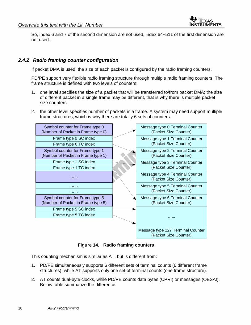
2.4.2 Radio framing counter configuration
If packet DMA is used, the size of each packet is configured by the radio framing counters.
PD/PE support very flexible radio framing structure through multiple radio framing counters. The frame structure is defined with two levels of counters:
1. one level specifies the size of a packet that will be transferred to/from packet DMA; the size of different packet in a single frame may be different, that is why there is multiple packet size counters.
2. the other level specifies number of packets in a frame. A system may need support multiple frame structures, which is why there are totally 6 sets of counters.
Symbol counter for Frame type 0
(Number of Packet in Frame type 0)
Frame type 0 TC index
Frame type 0 SC index
Message type 0 Terminal Counter
(Packet Size Counter)
Message type 1 Terminal Counter
(Packet Size Counter)
Message type 2 Terminal Counter
(Packet Size Counter)
Message type 3 Terminal Counter
(Packet Size Counter)
Message type 4 Terminal Counter
(Packet Size Counter)
Message type 5 Terminal Counter
(Packet Size Counter)
Message type 6 Terminal Counter
(Packet Size Counter)
…...
Message type 127 Terminal Counter
(Packet Size Counter)
Symbol counter for Frame type 1
(Number of Packet in Frame type 1)
Frame type 1 TC index
Frame type 1 SC index
…...
…...
…...
Symbol counter for Frame type 5
(Number of Packet in Frame type 5)
Frame type 5 TC index
Frame type 5 SC index
Figure 14. Radio framing counters
This counting mechanism is similar as AT, but is different from:
1. PD/PE simultaneously supports 6 different sets of terminal counts (6 different frame structures); while AT supports only one set of terminal counts (one frame structure).
2. AT counts dual-byte clocks, while PD/PE counts data bytes (CPRI) or messages (OBSAI). Below table summarize the difference.

Overwrite this text with the Lit. Number
AIF2 Programming 19
Table 9. Unit of radio framing counters
AT Dual-byte clocks
OBSAI OBSAI messages (16 bytes payload)
CPRI Groups of 4 bytes (PE) Groups of 16 bytes (PD)
An application may define up to 6 frame structures with above counters. Each channel can be configured to use one of these frame structures. For one channel, it can switch between one frame structure to another frame structure on any frame boundary.
Each AxC stream channel can be programmed with different AxC offset, the framing counters for that channel begin counting from the AxC offset, and packet are actually transferred from that AxC offset. Please note, in PD in CPRI mode, AxC Offset programmed in the number of four samples (QW), relative to the received CPRI link frame boundary (sync byte K28.5), so it is normally programmed as 0. For all other cases, the AxC offset is relative to AT frame boundary.
2.4.3 TDD configuration (with packet DMA only)
The actual TDD air channel is simplex but the SERDES is full duplex. What this results in is the impact that only half of the available SERDES bandwidth of AIF2 is usable when in TDD mode.
TDD mode can be supported by packet DMA, it is implement in following ways:
TX: only sends packet in active TDD time slots
RX: only receive packets in active TDD time slots
For TX, TDD_AXC mode should be enabled in PE, if it is turned on, PE will insert symbol only when it receives the packet from packet DMA. So, it is user’s responsibility to not push packets into the packet DMA TX queue during inactive TDD time slots; and for active TDD timer slots, user should take care the time to push packet into the TX queue. A packet should only be pushed into TX queue just one packet ahead, for example, if packet of LTE symbol N need be sent in active TDD time slot, then packet N must be pushed into the TX queue in the time period of symbol (N-1).
For RX, PD implements programmable bit map for each channel, each bit corresponds to one packet in a radio Frame, “1” means corresponding packet will be received, “0” means that packet will be dropped. Please note, in LTE protocol level, the TDD is controlled in the unit of sub frame, but the AIF2 PD TDD bit map is defined in the unit of packets, and one LTE sub frame includes multiple packets (symbols), so the LTE TDD “bit map” in sub frame should be expanded to PD TDD “bit map” in packets, that is, we need to program multiple bits to select each LTE symbol in a sub frame.
Overwrite this text with the Lit. Number
20 AIF2 Programming
2.5 DIO engines configuration
Data structure is the basis of software programming, understanding the antenna data buffer structure is very important for programming DIO.
There are three egress DIO engines and three ingress DIO engines. Each engine can be configured to support:
Uplink WCDMA antenna data format for RAC. It is also called “UL RSA” data format in some documents for compatibility with old AIF1.
Downlink WCDMA antenna data format for TAC.
User defined antenna data structure. For some application, WCDMA antenna stream may be processed by DSP core or RSA (Rake Search Accelerator) instead of RAC or TAC. For the case, the antenna data structure in DSP memory can be freely defined by software. A typical structure is collect antenna data for each stream into a separate buffer instead of interleaving antenna streams into a single buffer link RAC or TAC buffer.
The DIO example code with this application note defined three tests corresponding to above three data formats:
typedef enum
{
/*test (simulate) antenna data from AIF2 to RAC*/
WCDMA_AIF2_RAC_TEST = 0,
/*test (simulate) antenna data from TAC to AIF2*/
WCDMA_AIF2_TAC_TEST,
/*test AIF2 antenna data to/from DSP core buffer*/
WCDMA_AIF2_CORE_TEST
} WcdmaAif2TestType;
DIO can be looked as a customized EDMA for AIF2. Following table summarizes the DIO configuration parameters and compares to EDMA.
Table 10. DIO configuration parameters
DIO parameter Equivalent EDMA parameter
Number of quad words (at AIF2 DB buffer) ACNT
Number of AxC (at AIF2 DB buffer) BCNT
DBCN (Dio Buffer Channel Number) table (addressing inside AIF2 DB buffer)
N/A
Number of blocks CCNT
burst size (1,2,4 QW) (at DSP memory) ACNT
Burst address stride (at DSP memory) BIDX
Block address stride (at DSP memory) CIDX
DIO base address (at DSP memory) SRC, DST
Following sections describe the structure of each data format and corresponding configurations of DIO engine.

Overwrite this text with the Lit. Number
AIF2 Programming 21
2.5.1 DIO configuration for AIF2 Data buffer
Following figure and table show the key DIO configuration for AIF2 data buffer.
AIF2 data buffer
DIO buffer length for each channel (128 or 256 bytes)
Channel 0
Channel 1
Channel 2
Channel 3
Channel 4
Number of Quad word
per AxC per transfer
(1, 2 or 4)
…...
AxC 0 Channel number
AxC 1 Channel number
AxC N Channel number
Number
of AxC
per DIO
Buffer Channel
Number Table
Figure 15. DIO configuration for AIF2 data buffer
Table 11. DIO configuration for AIF2 data buffer
Parameters Configuration Comments
DIO buffer length 128 or 256 bytes For WCDMA stream, 128 bytes is OK. For LTE stream, 256 bytes should be used.
Number of Quad word per AxC
1, 2 or 4 Number of quad word (16 bytes) transferred by one trigger.
Number of AxC <= 64 Support maximum 64 antenna streams per DIO engine.
Each DIO engine has a DMA Buffer Channel Number Table (DBCNT), which is used to select channels be serviced by this DIO engine. With this flexible mechanism, the DIO does NOT require the channels to be continuous in AIF2 data buffer.
Each DIO engine is trigger by corresponding DIO events from AIF2 timer. With each trigger event, the DIO engine transfers a block of (number of quad word) x (number of AxC). For the next event, the DIO engine will increase the access pointer in each channel buffer by (number of quad word), if the address reaches the end of the buffer, the DIO will automatically wrap it to the beginning of the buffer. So, the buffer for each channel is actually used as a circular buffer by DIO engine.

Overwrite this text with the Lit. Number
22 AIF2 Programming
Please note, some configuration register fields should be configured with expected value minus one. For example, if you want to support 4 AxC, the num_axc field should be set as 4-1 = 3.
2.5.2 DIO configuration for RAC
The RAC supports 54 streams, but the buffer is organized for the size of 64 streams, the location for stream 54~63 are not used. The RAC input buffer is a circular buffer which can hold 32 chips of data. Following figure shows the RAC front end buffer organization.
Stream 0 Sample 0
Stream 0 Sample 1 …….
Stream 53 Sample 0
Stream 53 Sample 1
Stream 54 Sample 0 …….
Stream 63 Sample 1
Chip0~7 S0S0C0~7 S0S1C0~7 …… S53S0C0~7 S53S1C0~7 Not used …… Not used
Chip8~15 S0S0C8~15 S0S1C8~15 …… S53S0C8~15 S53S1C8~15 Not used …… Not used
Chip16~23 S0S0C16~23 S0S1C16~23 …… S53S0C16~23 S53S1C16~23 Not used …… Not used
Chip24~31 S0S0C24~31 S0S1C24~31 …… S53S0C24~31 S53S1C24~31 Not used …… Not used
16 Bytes
Chip 8n+0 Chip 8n+1 Chip 8n+3 …… Chip 8n+6 Chip 8n+7
2 bytes
8 bits I 8 Bits Q
Figure 16. RAC antenna data buffer structure
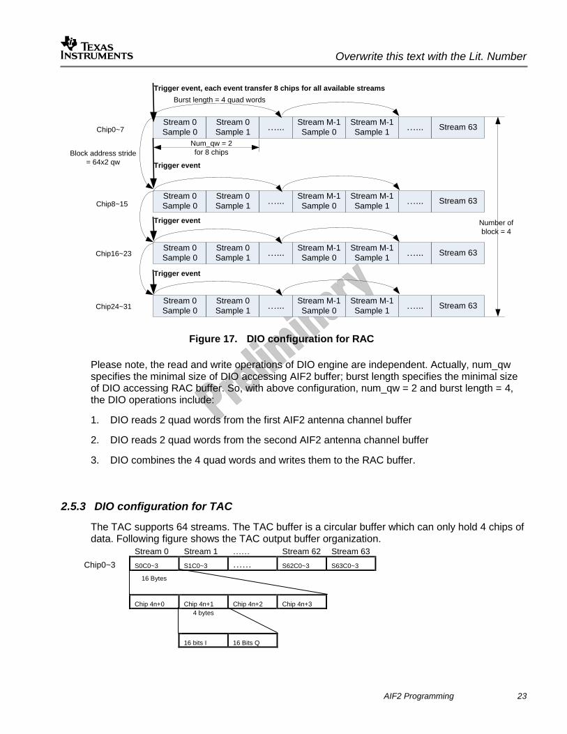
DIO is triggered every 8 chips for antenna data transferred to RAC. DIO transfers 8 chips for multiple streams with each trigger event. Following table shows the configuration of key DIO parameters for this case.
Table 12. DIO configuration for RAC
Parameters Configuration Comments
Number of Quad word per AxC
2 Corresponding to 8 chips
Number of AxC <= 54 Support maximum 54 antenna streams per RAC.
Number of blocks 4 4 x 8 = 32 chips, this is the size of RAC input buffer.
DMA burst length 4 quad words One burst include data of two antennas
burst address stride 4 quad words
block address stride 64 x 2 quad words
Following figure illustrates DIO transfer for RAC.
Overwrite this text with the Lit. Number
AIF2 Programming 23
Stream 0
Sample 0
Num_qw = 2
for 8 chips
Stream 0
Sample 1…...
Stream M-1
Sample 0…... Stream 63
Burst length = 4 quad words
Chip0~7
Block address stride
= 64x2 qw
Chip8~15
Number of
block = 4
Stream M-1
Sample 1
Stream 0
Sample 0
Stream 0
Sample 1…...
Stream M-1
Sample 0…... Stream 63
Stream M-1
Sample 1
Stream 0
Sample 0
Stream 0
Sample 1…...
Stream M-1
Sample 0…... Stream 63
Stream M-1
Sample 1
Stream 0
Sample 0
Stream 0
Sample 1…...
Stream M-1
Sample 0…... Stream 63
Stream M-1
Sample 1
Chip16~23
Chip24~31
Trigger event
Trigger event
Trigger event
Trigger event, each event transfer 8 chips for all available streams
Figure 17. DIO configuration for RAC
Please note, the read and write operations of DIO engine are independent. Actually, num_qw specifies the minimal size of DIO accessing AIF2 buffer; burst length specifies the minimal size of DIO accessing RAC buffer. So, with above configuration, num_qw = 2 and burst length = 4, the DIO operations include:
1. DIO reads 2 quad words from the first AIF2 antenna channel buffer
2. DIO reads 2 quad words from the second AIF2 antenna channel buffer
3. DIO combines the 4 quad words and writes them to the RAC buffer.
2.5.3 DIO configuration for TAC
The TAC supports 64 streams. The TAC buffer is a circular buffer which can only hold 4 chips of data. Following figure shows the TAC output buffer organization.
Stream 0 Stream 1 …… Stream 62 Stream 63
Chip0~3 S0C0~3 S1C0~3 …… S62C0~3 S63C0~3
16 Bytes
Chip 4n+0 Chip 4n+1 Chip 4n+2 Chip 4n+3
4 bytes
16 bits I 16 Bits Q

Overwrite this text with the Lit. Number
24 AIF2 Programming
Figure 18. TAC antenna data buffer structure
DIO is triggered every 4 chips for antenna data transferred from TAC. DIO transfers 4 chips for multiple streams with each trigger event. Following table shows the configuration of key DIO parameters for this case.
Table 13. DIO configuration for TAC
Parameters Configuration Comments
Number of Quad word per AxC
1 Corresponding to 4 chips
Number of AxC <= 64 Support maximum 64 antenna streams per TAC.
DMA burst length 4 quad words One burst include data of 4 antennas
burst address stride 4 quad words
block address stride 0 Wrap around to the beginning after every transfer
Number of blocks 32 Since block stride =0, any value for this field should be OK. But a relative larger number may reduce average DIO overhead.
Following figure illustrates DIO transfer for TAC.
Stream 0
num_qw = 1
for 4 chips
Stream 1 …... Stream M-1 …... Stream 64Chip0~3
Trigger event, each event transfer 4 chips for all available streams
Burst length = 4 quad words
Block
address
stride = 0
Figure 19. DIO configuration for TAC
Please note, the TAC buffer is a circular buffer, after one transfer, the next transfer will restart from the beginning of the buffer when next trigger event happens.
2.5.4 DIO configuration for antenna data buffer in DSP memory
For antenna stream be processed by DSP core or RSA (Rake Search Accelerator), the antenna data structure in DSP memory can be freely defined by software. Above buffer structure for RAC and TAC can also be used, but those structures interleave antenna streams, which is not good for DSP core to process them efficiently. A typical structure is to collect antenna data for each stream into separate buffers.

Overwrite this text with the Lit. Number
AIF2 Programming 25
For this case, the period of DIO trigger event can also be freely configured. The largest period, 16 chips, can be used to improve the throughput because the largest burst size can be utilized. Following table shows the configuration of key DIO parameters for this case.
Table 14. DIO configuration for antenna buffer in DSP memory
Parameters Configuration Comments
Number of Quad word per AxC
4 Corresponding to 16 chips
Number of AxC <= 64 Support maximum 64 antenna streams per DIO.
Number of blocks <= 8192 num_blks is a 13-bit field. So, the maximum buffer
size is limited to 8192*16= 131072 chips≈ 3.4
frames
DMA burst length 4 quad words One burst include data of 4 antennas
burst address stride Size of the buffer per AxC
brst_addr_stride is a 12-bit field. So, the maximum
buffer size is limited to 4096*4= 16384 chips≈ 6.4
WCDMA slots≈ 0.43 frames
block address stride 4 quad words
Following figure illustrates DIO transfer for antenna data buffer in DSP memory.
Chip 0~15 Chip 16~31 …...
Burst length =
block stride =
4 quad words
num_blks depends on buffer size
Stream 0
Burst address stride =
Size of the buffer per AxC
Stream 1 num_axc = M
Trigger event , each event transfer 16 chips for all available streams
Stream M-1
Chip 0~15 Chip 16~31 …...
Chip 0~15 Chip 16~31 …...
Trigger event
Chip 32~47 Chip 48~63
Chip 32~47 Chip 48~63
Chip 32~47 Chip 48~63
Trigger event Trigger event Trigger event
Figure 20. DIO configuration for antenna buffer in DSP memory

Overwrite this text with the Lit. Number
26 AIF2 Programming
3 Generic packet data over AIF2
AIF2 supports generic data transfer with packet DMA. Generic data can be transferred over control message slot (for OBSAI) or control words (for CPRI) in parallel with antenna stream. If one link is not used for antenna stream, generic data can also be transferred over AxC (Antenna stream Carrier) slots. Following table summarize the bandwidth for generic packet transfers in different cases.
Table 15. Generic data transfer in different cases
OBSAI CPRI
Over control message slots or control words
Bandwidth utilization is about 1/21 (one control message slot in every 21 message slots).
For 8x link, bandwidth is about 6.144*0.8*(16/19)*(399/400)/21= 196Mbps
(16/19 means 16 byte payload in a message with 19 bytes; 399/400 excludes the K28.5 in a message group with 400 bytes)
Packet Size = n*16 bytes (n>0)
Can use 4B/5B or NULL delimiter. Bandwidth utilization is about 1/16*(64-P)/64 (1/16 means one control word in every 16 words. P is the start pointer of generic data in the control words array with 64 rows).
For 8x link, assume NULL delimiter, P=20, bandwidth is about 4.9152*0.8/16*44/64= 168Mbps
Over AxC slots
Bandwidth utilization is about 20/21
For 8x link, bandwidth is about 6.144*0.8*(16/19) *(399/400)*(20/21)= 3.9Gbps
Packet Size = n*16 bytes (n>0)
4B/5B delimiter must be used; Bandwidth utilization is about (4/5)*(15/16).
For 8x link, bandwidth is about 4.9152*0.8*15/16*(4/5)= 2.9Gbps
Notes: The factor 0.8 in above formula is for 8B/10B coding.
OBSAI support generic message in nature. To support generic data transfer, CPRI need additional delimiter, 4B/5B or NULL delimiter can be used for generic data over control words, since 4B/5B introduce more overhead, so NULL delimiter can be used for generic data over control words to improve it. But for generic data over AxC slots in CPRI mode, 4B/5B must be used, which waste 20% bandwidth.
Generic packet mode does not support concept of time stamps in OBSAI. It does not support terminal counters such as those used when processing antenna carrier data. When transferring generic packet data the user does not need to follow strict concept of timing or packet size without worrying about PD or PE failing to process.
Additionally, CPRI packets cannot be starved, that is, packet DMA must transfer the data in time, if the latter data of a packet is not transfer in time by packet DMA, the PE will truncate the packet, thus RX side may receive a smaller packet without special notification. OBSAI has a mechanism for handling generic packet starvation, so, user does not need worry about this in OBSAI mode.
Overwrite this text with the Lit. Number
AIF2 Programming 27
AIF2 Egress Scheduler (ESCH) has a configuration (AD_ESCH_CFG.PRI) to control the priority between AxC channel and generic packet channel. For CPRI, this field should be set to 1, which actually gives same priority for AxC channel and generic packet channel. For OBSAI, this field can be leave as 0, which gives higher priority to AxC channel.
So, generally speaking, OBSAI mode supports generic data transfer better.
4 AIF2 debug tips
AIF2 is very complicated and relative hard for debug.
Some common debug methods, such as breakpoint, step through, or printf() during AIF2 running, may affects the operation of AIF2, because AIF2 is very timing sensitive, once these debug operation happens, AIF2 timing may be broken, so, after these operations, AIF2 may not function properly.
So, normally, for debug purpose, AIF2 status is checked after expected data have been transferred. Additionally, some AIF2 status registers are volatile after normal data transfer, when you manually check them, they may have changed. So, the best way is to dump AIF2 status registers to a data buffer or structure by software right after the expected data transfer completes. And then, user can check the data structure manually, or software can print these statuses later. The example code in “aif_debug.c” in the example projects for this application notes is implemented in this way.
The AIF2 statuses may be helpful for debug include:
AD EOP counter (24-bit), this counter will wrap when it reaches its maximum value.
In packet DMA mode, it counts the packet number.
In DIO mode, it counts the ingress data burst (normally, 64 bytes) only; egress DIO data is not counted.
AT frame, symbol/slot, clock count.
RM/TM state
Captured RM Pi offset
All other error/status
AIF2 EE module detects/monitors error/status of 18 AIF2 internal modules. For each of these modules, there is a set of registers defined for error/status reporting. Error happens in any module will trigger interrupt, and corresponding bit in ERR_ALRM_ORGN is set.

Overwrite this text with the Lit. Number
28 AIF2 Programming
EV0 Enable Set Register
EVO Enable Clear Register
Raw Status Set Register
Raw Status Clear Register
EV1 Enable Set Register
EV1 Enable Clear Register
Error Enabled Status
Register
Ra
w S
tatu
s R
eg
iste
rE
V0
En
ab
le R
eg
iste
rE
V1
En
ab
le R
eg
iste
r
Alarm Enabled Status
Register
VBUS interface
IRS_SET
IRS_CLR
EN
_E
V0
EN_SET_EV0
EN_CLR_EV0
EN_SET_EV1
EN_CLR_EV1
IRS
EN
_E
V1
EN
_S
TS
_E
V0
EN
_S
TS
_E
V1
Clock
Errors interrupt to DSP core
Alarms
ERR_ALRM_ORGN
Figure 21. AIF2 EE (Error and Exception) Module
The Interrupt Service Routine should:
1. check the ERR_ALRM_ORGN to determine which module has error
2. Check the EN_STS of that mondule to determine what the error is.
3. Clear the IRS
The common error and possible reason are summarized in following table.
Overwrite this text with the Lit. Number
AIF2 Programming 29
Table 16. AIF2 common errors and possible resaons
Errors Possible reasons
RM Line Code Violations, or RM not in SYNC state.
Hardware signal integrity is not good, or the other side of the AIF link does not run properly.
PI out of window The AIF2 event timing is not configured properly.
data shift the AIF2 AxC offset is not configured properly
PE DB did not have data for a channel
The packet DMA does not transfer data in time.
PE Symbol index in Navigator protocol specific header did not match for one or more symbol.
The packet is not pushed into the TX queue in correct time, or the symbol index in the protocol specific header is not set correctly.
Packet DMA descriptor starvation
The descriptors are not returned to the FDQ in time, or RX data is generated faster than processing.
5 Example Projects
The example codes along with this application note were originally developed on the dual C6670 EVM, which has two C6670 DSPs. Following figure shows the AIF connection between two DSPs on C6670 EVM. The 6 AIF links are used to allow the following in the default configuration:
Support 2 full DSP to DSP connections. The 2 connections can be used to test antenna data transfer between DSPs.
Support 4 full links connection to the AMC Connector.

Overwrite this text with the Lit. Number
30 AIF2 Programming
TCI6618 EVM
DSP 0
PHYT_SYNC/RADT_SYNC
Serdes clock
AIF2
Timer
153.6MHz
Clock
One shot trigger
DSP 1PHYT_SYNC/RADT_SYNC
Serdes clock
AIF2
SW
6
TIMO0
Lin
k 0
Lin
k 1
Link 2Link3
Link 4Link 5
Link 2Link 3
Link 4Link 5
To AMC
Connector
Figure 22. AIF connections between two DSPs on C6670 EVM
The example codes along with this application note demonstrate diversiform working modes of AIF2:
Protocol: OBSAI, CPRI
Radio Standard: LTE (FDD/TDD, normal/extended symbol), WCDMA, TD-SCDMA
Link rate: 2x, 4x, 8x
Change data buffer between LL2, SL2, DDR
Data Type
Antenna data only (on AxC slots)
Generic data only (on AxC slots)
Antenna data (on AxC slots) and generic data (on control slots)
Data Path
Internal loopback
External redirection (between 2 DSPs)
Following figures show different test data path.

Overwrite this text with the Lit. Number
AIF2 Programming 31
DSP 0
PE TM
PD RM
TX
SERDES
RX
SERDES
SERDES
RT
Figure 23. Internal loopback test
DSP 0
PE TM
PD RM
TX
SERDES
RX
SERDES
SERDES DSP 1
PETM
PDRM
TX
SERDES
RX
SERDES
SERDES
RT
RT
Figure 24. External redirection test
Please note, link 2~5 of two DSPs are not directly connected to each other on C6670 EVM, without external connection, they can only be used for internal loopback test.
The example can also be run on other TI EVMs, but since there is only one DSP on them, only internal loopback test can be run on them.
The directory structure of the projects is as below:
Overwrite this text with the Lit. Number
32 AIF2 Programming
Figure 25. Directory structure of example codes
Each of below folder is a project for a specific case:
AIF2_CPRI_LTE_FDD
AIF2_CPRI_LTE_TDD
AIF2_CPRI_TDSCDMA
AIF2_OBSAI_LTE_FDD
AIF2_OBSAI_LTE_TDD
The “AIF2_PktDMA” is a combined project supporting all above cases.
The “AIF2_CPRI_WCDMA” is examples for WCDMA in CPRI mode.
“common” folder includes some common code such as DDR initialization, Multicore navigator driver…
There is a “src” folder in each project. The contents of the codes are list in following table.
Table 17. Source files of the example codes
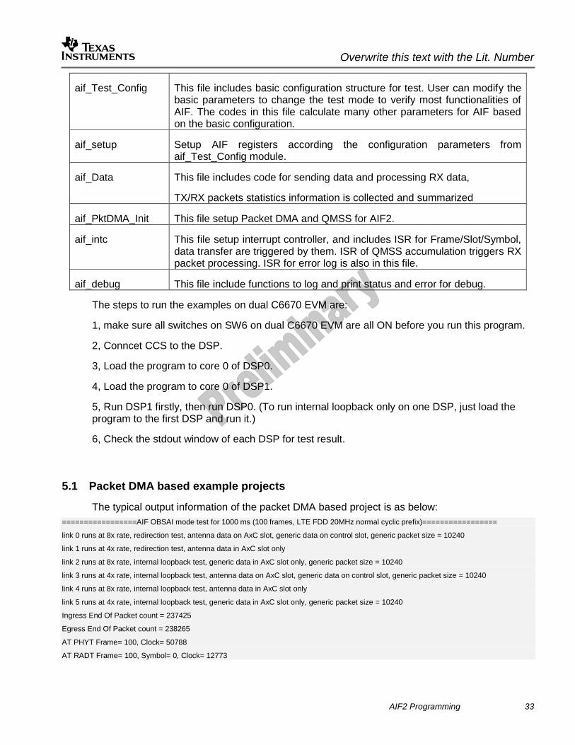
Files Descriptions
aif_main main() function and the top level control codes
Overwrite this text with the Lit. Number
AIF2 Programming 33
aif_Test_Config This file includes basic configuration structure for test. User can modify the basic parameters to change the test mode to verify most functionalities of AIF. The codes in this file calculate many other parameters for AIF based on the basic configuration.
aif_setup Setup AIF registers according the configuration parameters from aif_Test_Config module.
aif_Data This file includes code for sending data and processing RX data,
TX/RX packets statistics information is collected and summarized
aif_PktDMA_Init This file setup Packet DMA and QMSS for AIF2.
aif_intc This file setup interrupt controller, and includes ISR for Frame/Slot/Symbol, data transfer are triggered by them. ISR of QMSS accumulation triggers RX packet processing. ISR for error log is also in this file.
aif_debug This file include functions to log and print status and error for debug.
The steps to run the examples on dual C6670 EVM are:
1, make sure all switches on SW6 on dual C6670 EVM are all ON before you run this program.
2, Conncet CCS to the DSP.
3, Load the program to core 0 of DSP0.
4, Load the program to core 0 of DSP1.
5, Run DSP1 firstly, then run DSP0. (To run internal loopback only on one DSP, just load the program to the first DSP and run it.)
6, Check the stdout window of each DSP for test result.
5.1 Packet DMA based example projects
The typical output information of the packet DMA based project is as below:
=================AIF OBSAI mode test for 1000 ms (100 frames, LTE FDD 20MHz normal cyclic prefix)=================
link 0 runs at 8x rate, redirection test, antenna data on AxC slot, generic data on control slot, generic packet size = 10240
link 1 runs at 4x rate, redirection test, antenna data in AxC slot only
link 2 runs at 8x rate, internal loopback test, generic data in AxC slot only, generic packet size = 10240
link 3 runs at 4x rate, internal loopback test, antenna data on AxC slot, generic data on control slot, generic packet size = 10240
link 4 runs at 8x rate, internal loopback test, antenna data in AxC slot only
link 5 runs at 4x rate, internal loopback test, generic data in AxC slot only, generic packet size = 10240
Ingress End Of Packet count = 237425
Egress End Of Packet count = 238265
AT PHYT Frame= 100, Clock= 50788
AT RADT Frame= 100, Symbol= 0, Clock= 12773

Overwrite this text with the Lit. Number
34 AIF2 Programming
AT RADT captures Frame= 3, Symbol= 19, Clock= 153599 at PHYT boundary
----------------link 0 status----------------
captured PI value = 3250
RM ST3 State FRAME_SYNC
RM captured scrambling code = 0x0
TM FSM in FRAME_SYNC state
----------------link 1 status----------------
captured PI value = 3264
RM ST3 State FRAME_SYNC
TM FSM in FRAME_SYNC state
----------------link 2 status----------------
captured PI value = 3080
RM ST3 State FRAME_SYNC
RM captured scrambling code = 0x2
TM FSM in FRAME_SYNC state
----------------link 3 status----------------
captured PI value = 3085
RM ST3 State FRAME_SYNC
TM FSM in FRAME_SYNC state
----------------link 4 status----------------
captured PI value = 3080
RM ST3 State FRAME_SYNC
RM captured scrambling code = 0x4
TM FSM in FRAME_SYNC state
----------------link 5 status----------------
captured PI value = 3085
RM ST3 State FRAME_SYNC
TM FSM in FRAME_SYNC state
SL2_FDQ entry count = 133 (initial value 192)
AIF TX queue 0 entry count = 4
AIF TX queue 7 entry count = 2
AIF TX queue 8 entry count = 4
AIF TX queue 15 entry count = 3
generic Channel 0 transfer 1180 packets, receive 1175 packets (1175 good, 0 bad), 12032000 bytes in SL2, achieve 12 MB/s
AxC Channel 1 transfer 13861 packets, receive 13719 packets (13719 good, 0 bad), 120413632 bytes in SL2, achieve 121 MB/s
AxC Channel 2 transfer 13861 packets, receive 13719 packets (13719 good, 0 bad), 120413632 bytes in SL2, achieve 121 MB/s
AxC Channel 3 transfer 13861 packets, receive 13719 packets (13719 good, 0 bad), 120413632 bytes in SL2, achieve 121 MB/s
AxC Channel 4 transfer 13861 packets, receive 13719 packets (13719 good, 0 bad), 120413632 bytes in SL2, achieve 121 MB/s
Throughput of link 0 = 496 MB/s (56051 good packets, 0 bad packets)
AxC Channel 5 transfer 13861 packets, receive 13719 packets (13719 good, 0 bad), 120413632 bytes in SL2, achieve 121 MB/s
AxC Channel 6 transfer 13861 packets, receive 13719 packets (13719 good, 0 bad), 120413632 bytes in SL2, achieve 121 MB/s
Throughput of link 1 = 242 MB/s (27438 good packets, 0 bad packets)
generic Channel 7 transfer 46678 packets, receive 46673 packets (46673 good, 0 bad), 477931520 bytes in SL2, achieve 482 MB/s
Throughput of link 2 = 482 MB/s (46673 good packets, 0 bad packets)
Overwrite this text with the Lit. Number
AIF2 Programming 35
generic Channel 8 transfer 592 packets, receive 587 packets (587 good, 0 bad), 6010880 bytes in SL2, achieve 6 MB/s
AxC Channel 9 transfer 13861 packets, receive 13859 packets (13859 good, 0 bad), 121642432 bytes in SL2, achieve 122 MB/s
AxC Channel 10 transfer 13861 packets, receive 13859 packets (13859 good, 0 bad), 121642432 bytes in SL2, achieve 122 MB/s
Throughput of link 3 = 250 MB/s (28305 good packets, 0 bad packets)
AxC Channel 11 transfer 13861 packets, receive 13859 packets (13859 good, 0 bad), 121642432 bytes in SL2, achieve 122 MB/s
AxC Channel 12 transfer 13861 packets, receive 13859 packets (13859 good, 0 bad), 121642432 bytes in SL2, achieve 122 MB/s
AxC Channel 13 transfer 13861 packets, receive 13859 packets (13859 good, 0 bad), 121642432 bytes in SL2, achieve 122 MB/s
AxC Channel 14 transfer 13861 packets, receive 13859 packets (13859 good, 0 bad), 121642432 bytes in SL2, achieve 122 MB/s
Throughput of link 4 = 488 MB/s (55436 good packets, 0 bad packets)
generic Channel 15 transfer 23512 packets, receive 23507 packets (23507 good, 0 bad), 240711680 bytes in SL2, achieve 243 MB/s
Throughput of link 5 = 243 MB/s (23507 good packets, 0 bad packets)
Total throughput of AIF = 2201 MB/s (237410 good packets, 0 bad packets)
User can change the initialization values of basic configuration structure in “aif_Test_Config.c” as following and rebuild the project to verify most functionalities of AIF.
AifLinkConfig aifLinkCfg[6]=
{
/*Configuration for link 0*/
{
1, /*Link Enable: 1=enable, 0=disable*/
CSL_AIF2_LINK_RATE_8x,
TEST_PATH_INTERLNAL_LOOPBACK, /*test data path*/
AIF2_AXC_DATA_ONLY, /*testDataType*/
AIF_MONO_PACKET_SIZE-16, /*genericPacketSize*/
0, /*numberAxC: 0 means maximum number*/
LTE_20MHZ /*lteBandwidth*/
},
/*Configuration for link 1*/
{
1, /*Link Enable: 1=enable, 0=disable*/
CSL_AIF2_LINK_RATE_4x,
TEST_PATH_INTERLNAL_LOOPBACK, /*test data path*/
AIF2_AXC_DATA_ONLY, /*testDataType*/
AIF_MONO_PACKET_SIZE-16, /*genericPacketSize*/
2, /*numberAxC: 0 means maximum number*/
LTE_10MHZ /*lteBandwidth*/
},
/*Configuration for link 2*/
{
1, /*Link Enable: 1=enable, 0=disable*/
CSL_AIF2_LINK_RATE_2x,
TEST_PATH_INTERLNAL_LOOPBACK, /*test data path*/
AIF2_AXC_AND_GENERIC_DATA, /*testDataType*/
AIF_MONO_PACKET_SIZE-16, /*genericPacketSize*/
2, /*numberAxC: 0 means maximum number*/
LTE_5MHZ /*lteBandwidth*/
},
/*Configuration for link 3*/
{
1, /*Link Enable: 1=enable, 0=disable*/
CSL_AIF2_LINK_RATE_4x,
TEST_PATH_INTERLNAL_LOOPBACK, /*test data path*/
AIF2_GENERIC_DATA_ONLY, /*testDataType*/
Overwrite this text with the Lit. Number
36 AIF2 Programming
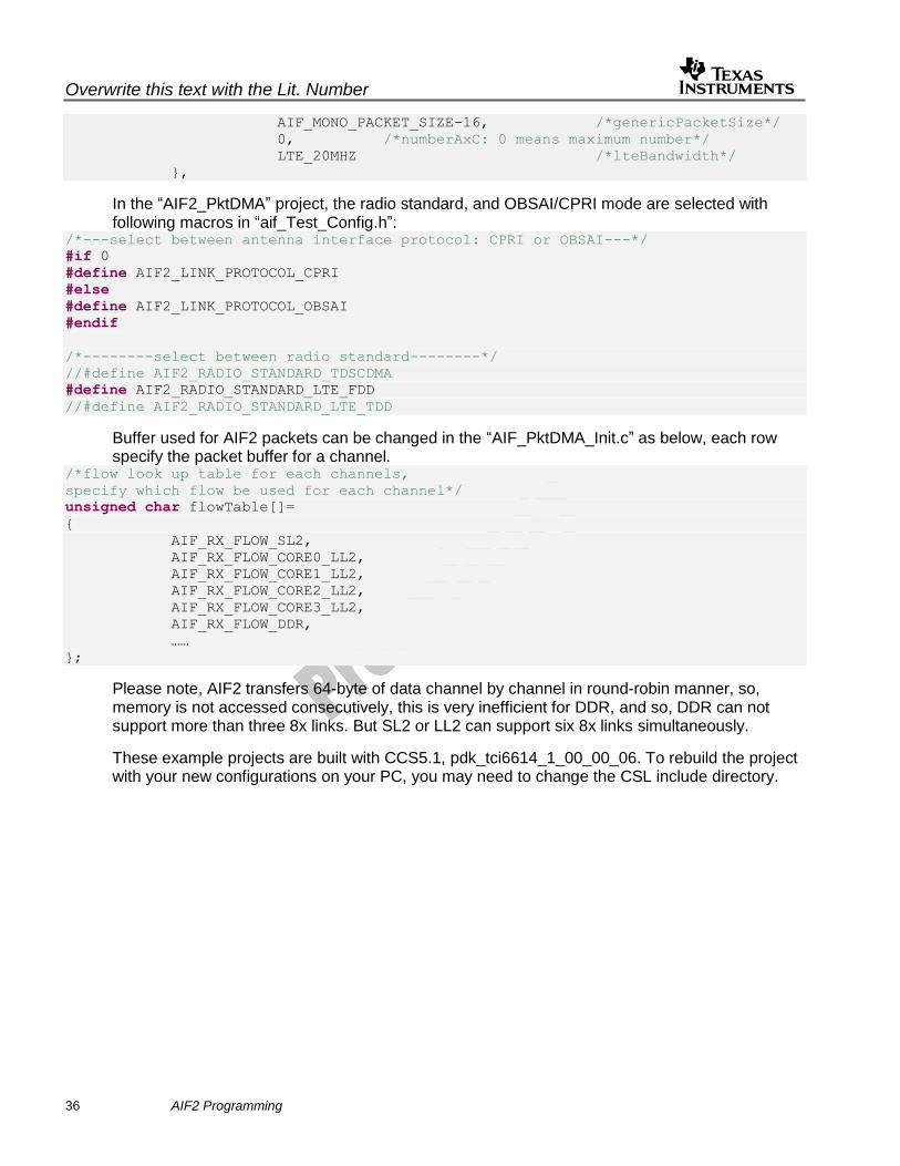
AIF_MONO_PACKET_SIZE-16, /*genericPacketSize*/
0, /*numberAxC: 0 means maximum number*/
LTE_20MHZ /*lteBandwidth*/
},
In the “AIF2_PktDMA” project, the radio standard, and OBSAI/CPRI mode are selected with following macros in “aif_Test_Config.h”:
/*---select between antenna interface protocol: CPRI or OBSAI---*/
#if 0
#define AIF2_LINK_PROTOCOL_CPRI
#else
#define AIF2_LINK_PROTOCOL_OBSAI
#endif
/*--------select between radio standard--------*/
//#define AIF2_RADIO_STANDARD_TDSCDMA
#define AIF2_RADIO_STANDARD_LTE_FDD
//#define AIF2_RADIO_STANDARD_LTE_TDD
Buffer used for AIF2 packets can be changed in the “AIF_PktDMA_Init.c” as below, each row specify the packet buffer for a channel.
/*flow look up table for each channels,
specify which flow be used for each channel*/
unsigned char flowTable[]=
{
AIF_RX_FLOW_SL2,
AIF_RX_FLOW_CORE0_LL2,
AIF_RX_FLOW_CORE1_LL2,
AIF_RX_FLOW_CORE2_LL2,
AIF_RX_FLOW_CORE3_LL2,
AIF_RX_FLOW_DDR,
……
};
Please note, AIF2 transfers 64-byte of data channel by channel in round-robin manner, so, memory is not accessed consecutively, this is very inefficient for DDR, and so, DDR can not support more than three 8x links. But SL2 or LL2 can support six 8x links simultaneously.
These example projects are built with CCS5.1, pdk_tci6614_1_00_00_06. To rebuild the project with your new configurations on your PC, you may need to change the CSL include directory.
Overwrite this text with the Lit. Number
AIF2 Programming 37
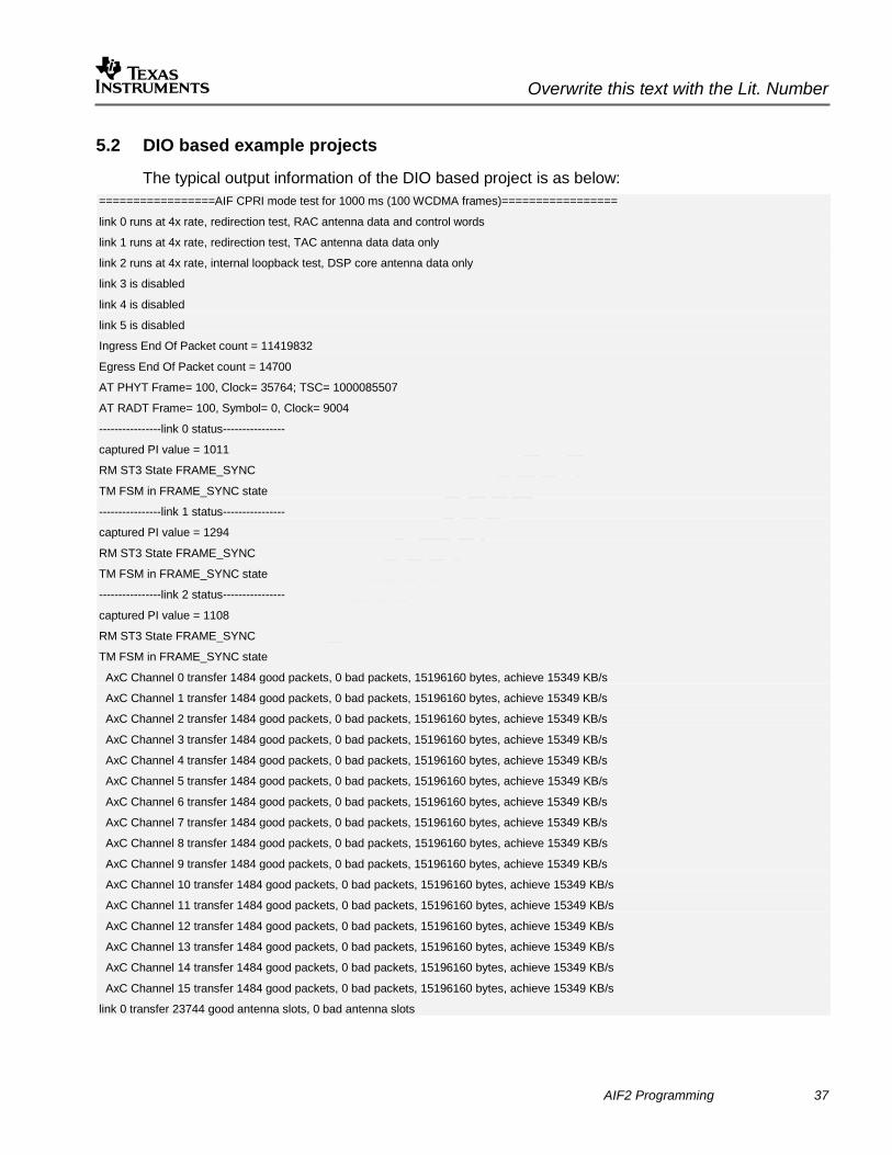
5.2 DIO based example projects
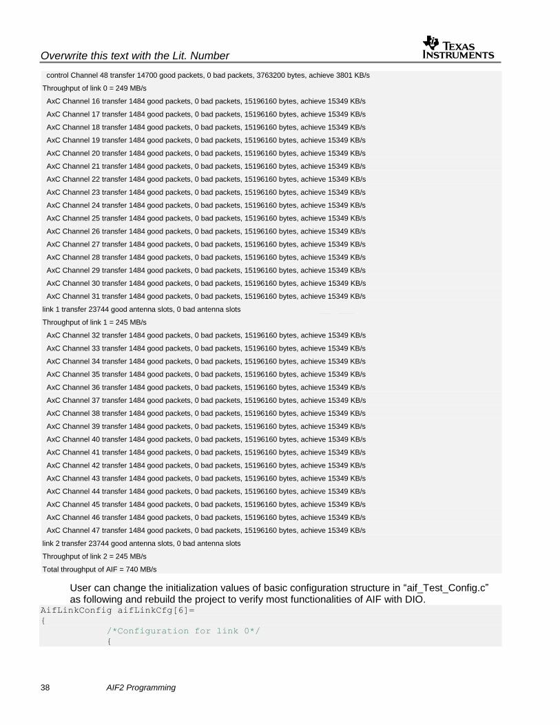
The typical output information of the DIO based project is as below:
=================AIF CPRI mode test for 1000 ms (100 WCDMA frames)=================
link 0 runs at 4x rate, redirection test, RAC antenna data and control words
link 1 runs at 4x rate, redirection test, TAC antenna data data only
link 2 runs at 4x rate, internal loopback test, DSP core antenna data only
link 3 is disabled
link 4 is disabled
link 5 is disabled
Ingress End Of Packet count = 11419832
Egress End Of Packet count = 14700
AT PHYT Frame= 100, Clock= 35764; TSC= 1000085507
AT RADT Frame= 100, Symbol= 0, Clock= 9004
----------------link 0 status----------------
captured PI value = 1011
RM ST3 State FRAME_SYNC
TM FSM in FRAME_SYNC state
----------------link 1 status----------------
captured PI value = 1294
RM ST3 State FRAME_SYNC
TM FSM in FRAME_SYNC state
----------------link 2 status----------------
captured PI value = 1108
RM ST3 State FRAME_SYNC
TM FSM in FRAME_SYNC state
AxC Channel 0 transfer 1484 good packets, 0 bad packets, 15196160 bytes, achieve 15349 KB/s
AxC Channel 1 transfer 1484 good packets, 0 bad packets, 15196160 bytes, achieve 15349 KB/s
AxC Channel 2 transfer 1484 good packets, 0 bad packets, 15196160 bytes, achieve 15349 KB/s
AxC Channel 3 transfer 1484 good packets, 0 bad packets, 15196160 bytes, achieve 15349 KB/s
AxC Channel 4 transfer 1484 good packets, 0 bad packets, 15196160 bytes, achieve 15349 KB/s
AxC Channel 5 transfer 1484 good packets, 0 bad packets, 15196160 bytes, achieve 15349 KB/s
AxC Channel 6 transfer 1484 good packets, 0 bad packets, 15196160 bytes, achieve 15349 KB/s
AxC Channel 7 transfer 1484 good packets, 0 bad packets, 15196160 bytes, achieve 15349 KB/s
AxC Channel 8 transfer 1484 good packets, 0 bad packets, 15196160 bytes, achieve 15349 KB/s
AxC Channel 9 transfer 1484 good packets, 0 bad packets, 15196160 bytes, achieve 15349 KB/s
AxC Channel 10 transfer 1484 good packets, 0 bad packets, 15196160 bytes, achieve 15349 KB/s
AxC Channel 11 transfer 1484 good packets, 0 bad packets, 15196160 bytes, achieve 15349 KB/s
AxC Channel 12 transfer 1484 good packets, 0 bad packets, 15196160 bytes, achieve 15349 KB/s
AxC Channel 13 transfer 1484 good packets, 0 bad packets, 15196160 bytes, achieve 15349 KB/s
AxC Channel 14 transfer 1484 good packets, 0 bad packets, 15196160 bytes, achieve 15349 KB/s
AxC Channel 15 transfer 1484 good packets, 0 bad packets, 15196160 bytes, achieve 15349 KB/s
link 0 transfer 23744 good antenna slots, 0 bad antenna slots
Overwrite this text with the Lit. Number
38 AIF2 Programming
control Channel 48 transfer 14700 good packets, 0 bad packets, 3763200 bytes, achieve 3801 KB/s
Throughput of link 0 = 249 MB/s
AxC Channel 16 transfer 1484 good packets, 0 bad packets, 15196160 bytes, achieve 15349 KB/s
AxC Channel 17 transfer 1484 good packets, 0 bad packets, 15196160 bytes, achieve 15349 KB/s
AxC Channel 18 transfer 1484 good packets, 0 bad packets, 15196160 bytes, achieve 15349 KB/s
AxC Channel 19 transfer 1484 good packets, 0 bad packets, 15196160 bytes, achieve 15349 KB/s
AxC Channel 20 transfer 1484 good packets, 0 bad packets, 15196160 bytes, achieve 15349 KB/s
AxC Channel 21 transfer 1484 good packets, 0 bad packets, 15196160 bytes, achieve 15349 KB/s
AxC Channel 22 transfer 1484 good packets, 0 bad packets, 15196160 bytes, achieve 15349 KB/s
AxC Channel 23 transfer 1484 good packets, 0 bad packets, 15196160 bytes, achieve 15349 KB/s
AxC Channel 24 transfer 1484 good packets, 0 bad packets, 15196160 bytes, achieve 15349 KB/s
AxC Channel 25 transfer 1484 good packets, 0 bad packets, 15196160 bytes, achieve 15349 KB/s
AxC Channel 26 transfer 1484 good packets, 0 bad packets, 15196160 bytes, achieve 15349 KB/s
AxC Channel 27 transfer 1484 good packets, 0 bad packets, 15196160 bytes, achieve 15349 KB/s
AxC Channel 28 transfer 1484 good packets, 0 bad packets, 15196160 bytes, achieve 15349 KB/s
AxC Channel 29 transfer 1484 good packets, 0 bad packets, 15196160 bytes, achieve 15349 KB/s
AxC Channel 30 transfer 1484 good packets, 0 bad packets, 15196160 bytes, achieve 15349 KB/s
AxC Channel 31 transfer 1484 good packets, 0 bad packets, 15196160 bytes, achieve 15349 KB/s
link 1 transfer 23744 good antenna slots, 0 bad antenna slots
Throughput of link 1 = 245 MB/s
AxC Channel 32 transfer 1484 good packets, 0 bad packets, 15196160 bytes, achieve 15349 KB/s
AxC Channel 33 transfer 1484 good packets, 0 bad packets, 15196160 bytes, achieve 15349 KB/s
AxC Channel 34 transfer 1484 good packets, 0 bad packets, 15196160 bytes, achieve 15349 KB/s
AxC Channel 35 transfer 1484 good packets, 0 bad packets, 15196160 bytes, achieve 15349 KB/s
AxC Channel 36 transfer 1484 good packets, 0 bad packets, 15196160 bytes, achieve 15349 KB/s
AxC Channel 37 transfer 1484 good packets, 0 bad packets, 15196160 bytes, achieve 15349 KB/s
AxC Channel 38 transfer 1484 good packets, 0 bad packets, 15196160 bytes, achieve 15349 KB/s
AxC Channel 39 transfer 1484 good packets, 0 bad packets, 15196160 bytes, achieve 15349 KB/s
AxC Channel 40 transfer 1484 good packets, 0 bad packets, 15196160 bytes, achieve 15349 KB/s
AxC Channel 41 transfer 1484 good packets, 0 bad packets, 15196160 bytes, achieve 15349 KB/s
AxC Channel 42 transfer 1484 good packets, 0 bad packets, 15196160 bytes, achieve 15349 KB/s
AxC Channel 43 transfer 1484 good packets, 0 bad packets, 15196160 bytes, achieve 15349 KB/s
AxC Channel 44 transfer 1484 good packets, 0 bad packets, 15196160 bytes, achieve 15349 KB/s
AxC Channel 45 transfer 1484 good packets, 0 bad packets, 15196160 bytes, achieve 15349 KB/s
AxC Channel 46 transfer 1484 good packets, 0 bad packets, 15196160 bytes, achieve 15349 KB/s
AxC Channel 47 transfer 1484 good packets, 0 bad packets, 15196160 bytes, achieve 15349 KB/s
link 2 transfer 23744 good antenna slots, 0 bad antenna slots
Throughput of link 2 = 245 MB/s
Total throughput of AIF = 740 MB/s
User can change the initialization values of basic configuration structure in “aif_Test_Config.c” as following and rebuild the project to verify most functionalities of AIF with DIO.
AifLinkConfig aifLinkCfg[6]=
{
/*Configuration for link 0*/
{
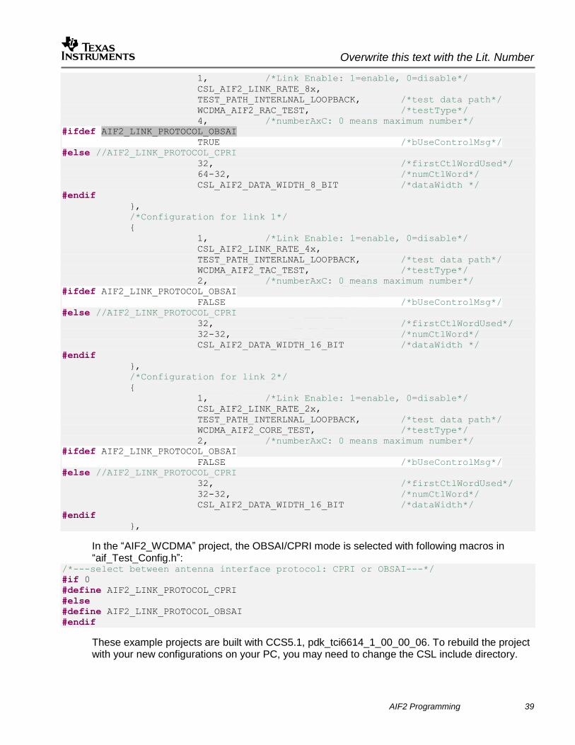
Overwrite this text with the Lit. Number
AIF2 Programming 39
1, /*Link Enable: 1=enable, 0=disable*/
CSL_AIF2_LINK_RATE_8x,
TEST_PATH_INTERLNAL_LOOPBACK, /*test data path*/
WCDMA_AIF2_RAC_TEST, /*testType*/
4, /*numberAxC: 0 means maximum number*/
#ifdef AIF2_LINK_PROTOCOL_OBSAI
TRUE /*bUseControlMsg*/
#else //AIF2_LINK_PROTOCOL_CPRI
32, /*firstCtlWordUsed*/
64-32, /*numCtlWord*/
CSL_AIF2_DATA_WIDTH_8_BIT /*dataWidth */
#endif
},
/*Configuration for link 1*/
{
1, /*Link Enable: 1=enable, 0=disable*/
CSL_AIF2_LINK_RATE_4x,
TEST_PATH_INTERLNAL_LOOPBACK, /*test data path*/
WCDMA_AIF2_TAC_TEST, /*testType*/
2, /*numberAxC: 0 means maximum number*/
#ifdef AIF2_LINK_PROTOCOL_OBSAI
FALSE /*bUseControlMsg*/
#else //AIF2_LINK_PROTOCOL_CPRI
32, /*firstCtlWordUsed*/
32-32, /*numCtlWord*/
CSL_AIF2_DATA_WIDTH_16_BIT /*dataWidth */
#endif
},
/*Configuration for link 2*/
{
1, /*Link Enable: 1=enable, 0=disable*/
CSL_AIF2_LINK_RATE_2x,
TEST_PATH_INTERLNAL_LOOPBACK, /*test data path*/
WCDMA_AIF2_CORE_TEST, /*testType*/
2, /*numberAxC: 0 means maximum number*/
#ifdef AIF2_LINK_PROTOCOL_OBSAI
FALSE /*bUseControlMsg*/
#else //AIF2_LINK_PROTOCOL_CPRI
32, /*firstCtlWordUsed*/
32-32, /*numCtlWord*/
CSL_AIF2_DATA_WIDTH_16_BIT /*dataWidth*/
#endif
},
In the “AIF2_WCDMA” project, the OBSAI/CPRI mode is selected with following macros in “aif_Test_Config.h”:
/*---select between antenna interface protocol: CPRI or OBSAI---*/
#if 0
#define AIF2_LINK_PROTOCOL_CPRI
#else
#define AIF2_LINK_PROTOCOL_OBSAI
#endif
These example projects are built with CCS5.1, pdk_tci6614_1_00_00_06. To rebuild the project with your new configurations on your PC, you may need to change the CSL include directory.

Overwrite this text with the Lit. Number
40 AIF2 Programming
5.3 To use these example code on other boards
To use these example code on other boards, below may need be changed:
1. on other board, if timer is not used to trigger the AIF2, other methods must be used. For example, for simple test, the AIF2 can be triggered by manually writing specific registers. This can be enabled by the macro defined in the “aif_Test_Config.h”:
//#define AIF2_TRIGGER_MANUALLY
2. on other boards, the reference clock for AIF2 may be different, this can be configured with following code in “aif_setup.c”
#ifdef AIF2_LINK_PROTOCOL_OBSAI
pllMpy= CSL_AIF2_PLL_MUL_FACTOR_20X; /*153.6*20=3072*/
#else
pllMpy= CSL_AIF2_PLL_MUL_FACTOR_16X; /*153.6*16=2457.6*/
#endif
3. DSP core PLL and DDR configuration may need be changed in “aif_main.c”, or GEL or other methods should be used to initialize them.
//DSP core speed: 122.88*236/29= 999.9889655MHz
KeyStone_main_PLL_init(122.88, 236, 29);
//DDR init 66.667*20/1= 1333
KeyStone_DDR_init (66.667, 20, 1);

Overwrite this text with the Lit. Number
AIF2 Programming 41
References 1. KeyStone Architecture Antenna Interface 2 (AIF2) User Guide (sprugv7)
2. Multicore Navigator for KeyStone Devices User's Guide (sprugr9)
3. TMS320C66x CorePac User's Guide (sprugw0)
4. TMS320C6670 datasheet (SPRS688)