aixtron investor presentation · aixtron investor presentation ir presentation – h1/2015 ......
TRANSCRIPT

AIXTRON Investor Presentation IR Presentation – H1/2015 (FSE: AIXA, ISIN DE000A0WMPJ6, NASDAQ: AIXG, ISIN: US0096061041)
© AIXTRON Investor Relations, September 2015
Forward-Looking Statements
This document may contain forward-looking statements regarding the business, results of operations, financial condition and earnings outlook of AIXTRON within the meaning of the safe harbor provisions of the US Private Securities Litigation Reform Act of 1995. These statements may be identified by words such as “may”, “will”, “expect”, “anticipate”, “contemplate”, “intend”, “plan”, “believe”, “continue” and “estimate” and variations of such words or similar expressions. These forward-looking statements are based on our current views and assumptions and are subject to risks and uncertainties. You should not place undue reliance on these forward-looking statements. Actual results and trends may differ materially from those reflected in our forward-looking statements. This could result from a variety of factors, such as actual customer orders received by AIXTRON, the level of demand for deposition technology in the market, the timing of final acceptance of products by customers, the condition of financial markets and access to financing for AIXTRON, general conditions in the market for deposition plants and macroeconomic conditions, cancellations, rescheduling or delays in product shipments, production capacity constraints, extended sales and qualification cycles, difficulties in the production process, the general development in the semi-conductor industry, increased competition, fluctuations in exchange rates, availability of public funding, fluctuations and/or changes in interest rates, delays in developing and marketing new products, a deterioration of the general economic situation and any other factors discussed in any reports or other announcements field by AIXTRON with the U.S. Securities and Exchange Commission. Any forward-looking statements contained in this document are based on current expectations and projections of the Executive Board and on information currently available to it and are made as at the date hereof. AIXTRON undertakes no obligation to revise or update any forward-looking statements as a result of new information, future events or otherwise, unless expressly required to do so by law.
AIXTRON INVESTOR PRESENTATION
2

Who we are
Headquarters based in Herzogenrath, Germany
Worldwide presence with 12 sales/representatives offices
and production facilities
Company founded in 1983 – over 30 years of experience
~760 employees
Technology leader in deposition systems
More than 3,000 deposition systems delivered
all over the world
State of the art R&D center and demo facilities
Annual R&D budget of approx. € 55-65 Million
3 ABOUT AIXTRON

Our Technology. Your FUTURE.
AIXTRON TECHNOLOGIES 4
Compound Semiconductors
Silicon Semiconductors
Organic
Carbon
LED Lighting Memory & Logic
OLED Power Management

Equipment Order Intake per Quarter
OPERATIONS 5
Source: Deutsche Bank Equity Research, AIXTRON SE
0
50
100
150
200
250
1Q98
2Q98
3Q98
4Q98
1Q99
2Q99
3Q99
4Q99
1Q00
2Q00
3Q00
4Q00
1Q01
2Q01
3Q01
4Q01
1Q02
2Q02
3Q02
4Q02
1Q03
2Q03
3Q03
4Q03
1Q04
2Q04
3Q04
4Q04
1Q05
2Q05
3Q05
4Q05
1Q06
2Q06
3Q06
4Q06
1Q07
2Q07
3Q07
4Q07
1Q08
2Q08
3Q08
4Q08
1Q09
2Q09
3Q09
4Q09
1Q10
2Q10
3Q10
4Q10
1Q11
2Q11
3Q11
4Q11
1Q12
2Q12
3Q12
4Q12
1Q13
2Q13
3Q13
4Q13
1Q14
2Q14
3Q14
4Q14
1Q15
2Q15
Compound Semiconductor Market China Investments
driven by notebook
backlighting
driven by LED TV
driven by strategic China investments
(EUR million)
driven by mobile phone
penetration
driven by telecom/datacom and mobile phone

LED Lighting Market: Multiple Tipping Points
INDUSTRY & MARKETS 6
Various Applications
Different Regions
Numerous Players
LED Lighting Cycle
Source: : AIXTRON, McKinsey 2012

Compound Semiconductors
MOCVD ALD/MOCVD
LEDs, Lasers and
Optoelectronics
• LEDs for display: TVs, mobile phones, tablets, etc.
• LEDs for lighting
• LEDs for automotive
• LEDs for datacom
• Lasers for telecom,
consumer electronics
• Photovoltaics
Increasing Equipment
Demand Expected by:
2015
Our Technology Portfolio
7
Silicon Semiconductors
• RF transistors
• AC-DC converters
• DC-DC converters
• Solar inverters
• Motor drives in industrial applications automotive and consumer electronics
Power Management GaN / SiC
• DRAM Dielectric and Metal Electrode
• Flash Inter Poly Dielectric and Metals
• Logic Gate stack
• ReRAM and PCRAM Active element and Electrode
• Logic High Mobility Channel
Silicon Semiconductors
Increasing Equipment
Demand Expected by:
2015
Increasing Equipment
Demand Expected by:
2015/2016
• OLEDs for display: TVs, mobile phones, tablets, etc.
• Thin Film Encapsulation
• OLEDs for lighting
• Organic, flexible electronics
• Organic Photovoltaics
• Transistors
• Interconnects
• Flexible Electronics
• Energy Storage
• Sensors, etc.
Organic Electronics Graphene,
CNTs and CNWs
Organic Carbon
OVPD®/PVPD®/TFE PECVD
Increasing Equipment
Demand Expected by:
2016/2017
Increasing Equipment
Demand Expected by:
Beyond 2018
AIXTRON TECHNOLOGIES AND PRODUCTS

H1/2015 Financial Highlights
Sales: Volume below expectations due to delays in AIX R6 shipments
Gross Margin: Lower than expected due to impact from AIX R6 qualification process
OPEX on track: EUR 39.1m (target run-rate around EUR 80m on an annual basis)
Solid Cash Position: EUR 255.4m as of June 30, 2015 (EUR 268.1m as of Dec 31, 2014)
Order Backlog: EUR 91.2m as of June 30, 2015 (EUR 69.0m as of Jan 1st, 2015)
FINANCIALS 8
Market Prospects
Short-Term • Further increasing adoption of LEDs for exterior, public infrastructure & commercial lighting
• Increased adoption of LEDs for consumer & residential lighting
• Market positioning of the new AIX R6 MOCVD tool for LED manufacturing
• Increasing adoption of GaN for power electronics
• Increased emergence of silicon carbide (SiC) hybrid automotive & photovoltaic applications
• Next generation NAND, DRAM & PRAM memory applications
Mid- to Long-Term • Development of organic semiconductors applications using efficient deposition and thin-film
encapsulation technologies
• Development of GaN-on-Si based power electronics or LEDs
• Further development of plastic electronics/flexible TFT backplanes
• Increased development for specialized compound solar cells
• Higher demand for High-k as well as interconnect components
• Progress in the convergence of compound material applications, e. g. substituting materials in the silicon semiconductor industry
• Development of applications using carbon nanostructures including graphene
FUTURE MARKETS 9

AIXTRON INVESTOR PRESENTATION 10

Technology Position
AIXTRON TECHNOLOGIES AND PRODUCTS 11
R&D Demo &Qualification Pilot Production High Volume Production
MOCVD for III-V on Silicon
Carbon
Thin-Film Encapsulation for
OLED
OVPD for OLED deposition
ALD for Memory Customer B & C
ALD for Memory Customer A
MOCVD for LEDs, Lasers and
Optoelectronics
MOCVD for Power Management

0
10,000
20,000
30,000
40,000
50,000
60,000
2014e
2015e
2016e
2017e
2018e
HB L
ED
Mark
et (2
" Equiv
ale
nt W
afe
r in
000)
Mobile & Others Display Lighting
Increasing LED Area Demand Driving Growth
INDUSTRY & MARKETS 12
0
50
100
150
2014e
2015e
2016e
2017e
2018e
HB L
ED
Mark
et (b
n u
nits)
Mobile & Others Display Lighting
• Growth through increasing LED-unit and area demand
• Consistent epitaxial area growth will trigger equipment demand
• LED-lighting gaining further momentum
Based on compilation of latest opinions by: DisplaySearch; Strategies Unlimited; Displaybank; Gartner Dataquest; IMS Research.; McKinsey Lighting Report
(0.1mm²) (0.25mm²) (0.75-1mm²)
LED Units 2” Equivalent Wafer
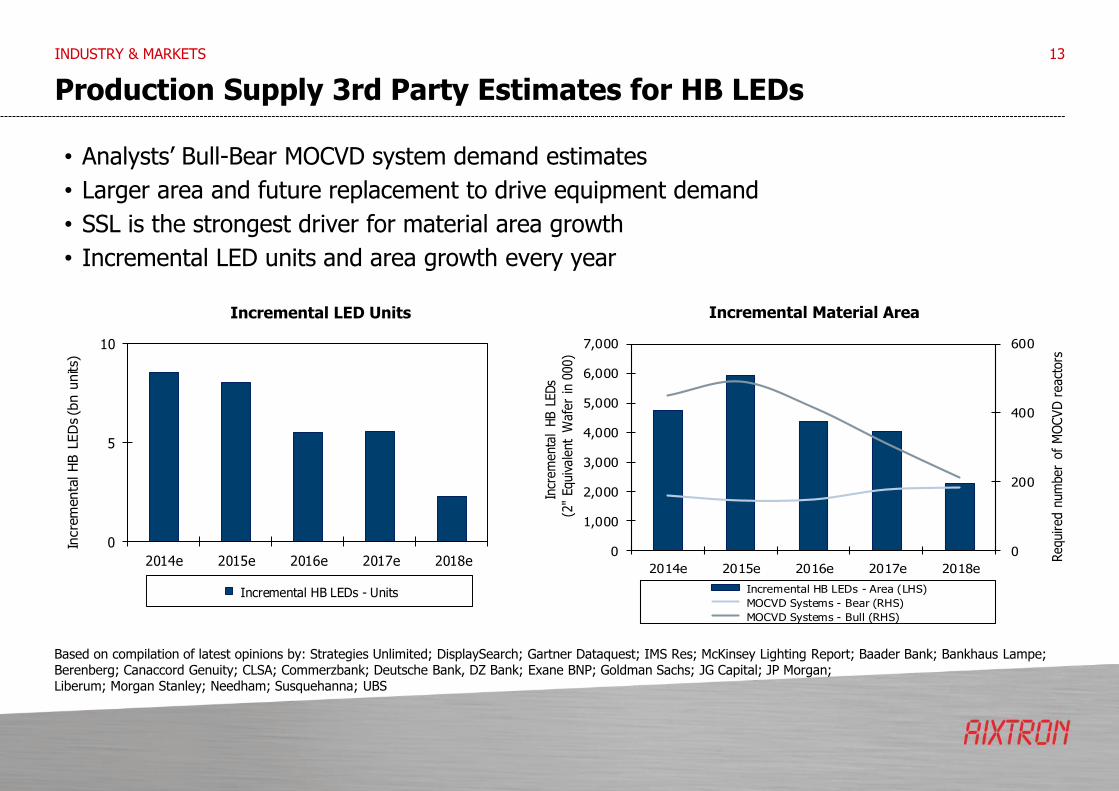
Production Supply 3rd Party Estimates for HB LEDs
INDUSTRY & MARKETS 13
• Analysts’ Bull-Bear MOCVD system demand estimates
• Larger area and future replacement to drive equipment demand
• SSL is the strongest driver for material area growth
• Incremental LED units and area growth every year
Based on compilation of latest opinions by: Strategies Unlimited; DisplaySearch; Gartner Dataquest; IMS Res; McKinsey Lighting Report; Baader Bank; Bankhaus Lampe; Berenberg; Canaccord Genuity; CLSA; Commerzbank; Deutsche Bank, DZ Bank; Exane BNP; Goldman Sachs; JG Capital; JP Morgan; Liberum; Morgan Stanley; Needham; Susquehanna; UBS
Incremental LED Units Incremental Material Area
0
5
10
2014e 2015e 2016e 2017e 2018e
Incre
menta
l H
B L
ED
s (b
n u
nits)
Incremental HB LEDs - Units
0
200
400
600
0
1,000
2,000
3,000
4,000
5,000
6,000
7,000
2014e 2015e 2016e 2017e 2018e
Required n
um
ber
of
MO
CVD r
eact
ors
Incr
em
enta
l HB L
EDs
(2"
Equiv
ale
nt
Wafe
r in
000)
Incremental HB LEDs - Area (LHS)
MOCVD Systems - Bear (RHS)
MOCVD Systems - Bull (RHS)

Compound Semiconductors – Power Electronics
AIXTRON TECHNOLOGIES AND PRODUCTS 14
Consumer Electronics & IT Automotive Energy Industrial
Power Management
GaN
• Electronic appliances
• Computing
• Wireless charging
• Power supplies
• PFC
• Infotainment
• GPS
• Connected car
• Autonomous driving
• EMI/EMC
• Adaptive cruise control
GaN / SiC
• General Automotive
Electronics
• HEV/EV
• Charging stations
• Inverter / motor drives
• Converter
• Radar test applications
• Power Grid / Smart Meter / Appliances
• Solar / Wind inverters
• Solar / Wind Power
DC distribution
• Power Storage
• UPS
• UPS
• Industrial machines
• Building
• Mining, oil, gas power
generation
• Shipping/Rail
SiC
Power Switching
30V 600V 1.2 kV ≥2kV
Volume segment Niche segment

Compound Semiconductors – MOCVD System Generations
• Extendibility: Extensive choice of configurations and enhancements
• Scalability: Multiple technologies on one platform
• Productivity: Highest throughput, best yield, fastest growth rates
Two Reactor Technologies Planetary Reactor® & Close Coupled Showerhead® (CCS)
AIXTRON TECHNOLOGIES AND PRODUCTS
15
Year of Introduction Technology Chambers
2002 • G3 Planetary
• 19x2” CCS
• 24x2”, 8x4”
• 19x2”
2006 • G4 HT Planetary
• CRIUS® CCS
• 42x2”, 11x4”, 6x6”
• 31x2”, 12x3”, 7x4”, 3x6”, 1x12”
2010/ 2011 • G5 HT Planetary
• CRIUS® II-eXL CCS
• 56x2”, 14x4”, 8x6’’, 5x8’’
• 75x2”, 19x4”
2012 • G5+ HT Planetary • 5x8” GaN-on-Si Technology
2014 • G5 WW
• AIX R6
• 12x4”, 8x6”
• 121x2”, 31x4”, 12x6”

Compound Semiconductors – MOCVD
• Addressing multiple industries
• Established industry standard & market leading
• Configurable, extendable common platform
• Introduced the latest MOCVD technology - AIX R6
Two Reactor Technologies Planetary Reactor® & Close Coupled Showerhead® (CCS)
AIXTRON TECHNOLOGIES AND PRODUCTS 16
Planetary Reactor®
AIX G5+, 5x8 Close Coupled Showerhead®
AIX R6, 31x4”
• Unique Planetary reactor design
• Horizontal reactor type
• Patented CCS Technology
• Vertical reactor design

Organic Electronics – OVPD® + Encapsulation
AIXTRON TECHNOLOGIES AND PRODUCTS 17
Source: DisplaySearch, AIXTRON
Front-end Array process equipment
Front-end Cell process equipment
Coating
Etching
Stripping
Test and repair
ITO deposition
Cleaning
Organic material deposition
Encapsulation
Cathode deposition
Cleaning Glass cutting
Bonding
Aging
Final test
Back-end Module process equipment
Targeted technology
OLED manufacturing process

Organic Electronics – Front-end Process Equipment
AIXTRON TECHNOLOGIES AND PRODUCTS
18
Cleaning Deposition Cathode
deposition Encapsulation Module
preparation Automation
5%
40%
10% 20%
5%
20%
Cumulative Capex
45%
55%
75%
80%
100%
Focus Activities
Key competency: Thin-film deposition
Value creation: 60%
Source: IHS; AIXTRON internal estimates

Organic Electronics – OVPD®
19
• Proprietary carrier-gas enhanced gas phase deposition approach for organic thin films
• Based on AIXTRON‘s core competence of carrier gas enhanced vapor phase deposition
• Free scalability: suitable for all relevant substrate generations
• Manufacturing technology applicable for OLED displays, OLED lighting, organic semiconductors, and organic photovoltaic
• High deposition rates for high throughput • Reduced thermal stress for organic materials
• High material utilization efficiency • Flexible process control
• Simplified scaling due to
• Close Coupled Showerhead and • Decoupled source technology
• Flexible integration solutions for batch and inline
• Reduced number of deposition chamber and footprint
Product Description – OVPD®
Product Features
“Disruptive deposition technology for cost efficient OLED manufacturing”
AIXTRON TECHNOLOGIES AND PRODUCTS

Carbon Nanostructures – PECVD
20
Product features
• Proprietary thermal and plasma enhanced chemical vapour deposition technology
• Excellent uniformity and reproducibility with fast turnaround cycle times
• BM platform: BM R&D (2-inch), BM Pro (4-inch and 6-inch), BM GB (4-inch glovebox), BM HT (high temperature, 1,700C), BM300T (300mm)
• Graphene and carbon nanotube films for electronics, energy storage, thermal management, sensors and flexible/transparent applications
Graphene and Carbon Nanotube Deposition Systems
• Fast response heater and turnaround
• Thermal CVD
• Substrate and top heating
• Closed loop infrared wafer temperature control
• Plasma enhanced CVD with frequency control
• Flexible processing for different applications
• Low cost of ownership
• Easy maintenance and cleaning
• User management features and growth library
Graphene (2D) and Carbon nanotube (1D)
Unique combination of high electrical/ thermal conductivity, mobility, flexibility and transparency
Serving R&D market today
AIXTRON BM Pro
Production ready for tomorrow
AIXTRON BM300T
Material Properties
AIXTRON Technology
Enabling Applications
AIXTRON TECHNOLOGIES AND PRODUCTS

Silicon Semiconductors – ALD
21
Product Description – ALD
• Up to 3 patented TriJet vaporizers
• Small volume confined process space ensure short ALD cycle time
• > 40 % less precursor consumption • Efficient purge
• Isolated multi wafer processing with
> 40% higher throughput
• Close Coupled Showerhead for uniform distribution
• Flexibility and ease of maintenance
• 300mm ALD Technology
• QXP-8300 Mini-batch system
• High throughput : 2 Process Chambers – 8 stations
• Up to 3 vaporizers and one bubbler
• Applications : DRAM, Logic and Flash High k Dielectric Metal electrode : ReRAM and PCRAM Active elements
• Proven in HVM with >40% lower CoO and >90% Uptime in DRAM and Flash Fabs
“Best-in class technology, state of the art deposition system, lowest CoO”
AIXTRON TECHNOLOGIES AND PRODUCTS
Product Features
Silicon Semiconductors – ALD and MOCVD
22
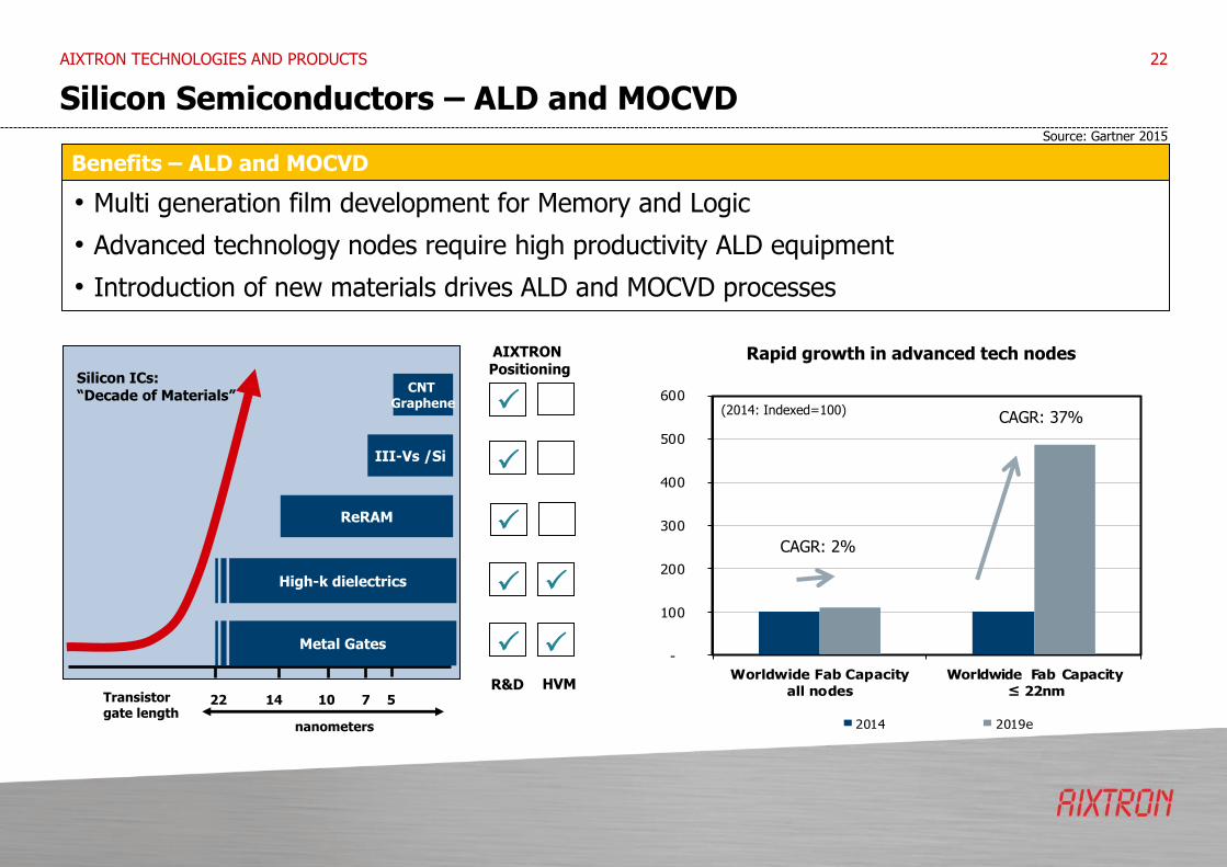
Benefits – ALD and MOCVD
• Multi generation film development for Memory and Logic
• Advanced technology nodes require high productivity ALD equipment
• Introduction of new materials drives ALD and MOCVD processes
AIXTRON TECHNOLOGIES AND PRODUCTS
-
100
200
300
400
500
600
Worldwide Fab Capacity
all nodes
Worldwide Fab Capacity
≤ 22nm
2014 2019e
ReRAM
III-Vs /Si
nanometers
22 Transistor gate length
10
CNT Graphene
14 7
Silicon ICs: “Decade of Materials”
R&D HVM
AIXTRON Positioning
Source: Gartner 2015
(2014: Indexed=100) CAGR: 37%
CAGR: 2%
Rapid growth in advanced tech nodes
5
Metal Gates
High-k dielectrics
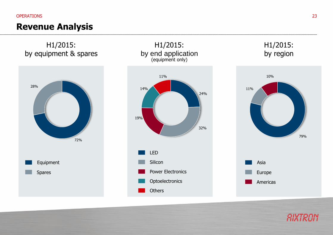
Revenue Analysis
OPERATIONS 23
H1/2015: by region
H1/2015: by equipment & spares
72%
28%
Spares
Equipment
H1/2015: by end application
(equipment only)
24%
32%
19%
14%
11%
79%
11%
10%
Americas
Europe
Asia
Power Electronics
Silicon
LED
Optoelectronics
Others

Consolidated Income Statement*
24
(€ million) H1/15 H1/14
Restated +/- Q2/15 Q1/15 +/-
Revenues 80.7 90.1 -10% 40.4 40.3 0%
Cost of sales 68.3 67.61 1% 36.8 31.5 17%
Gross profit 12.4 22.61 -45% 3.6 8.8 -59%
Gross Margin 15% 25%1 -10 pp 9% 22% -13 pp
Selling expenses 6.3 6.41 -2% 3.0 3.3 -9%
General & admin expenses 8.5 9.6 -11% 4.2 4.3 -2%
R&D 27.6 29.2 -6% 14.6 12.9 13%
Net other op.(income)/expenses -3.3 -1.3 -154% -0.3 -3.0 -90%
EBITDA -21.8 -13.4 -63% -15.3 -6.4 -139%
EBIT -26.7 -21.5 -24% -17.9 -8.8 -103%
EBIT Margin -33% -24% -9 pp -44% -22% -22 pp
Result before tax -26.2 -20.8 -26% -17.7 -8.5 -108%
Pre-Tax Margin -33% -23% -10 pp -44% -21% -23 pp
Net result -27.6 -23.4 -18% -18.1 -9.5 -91%
Net Return on Sales -34% -26% -8 pp -45% -23% -22 pp
FINANCIALS
*) rounded figures; may not add up 1) Restated; please refer to “Accounting Policies” in H1-Report

Consolidated Statement of Financial Position*
25
(€ million) 30/6/15 31/12/14 30/6/14
Property, plant & equipment 80.6 77.3 78.3
Goodwill 77.1 64.8 64.5
Other intangible assets 5.7 2.5 2.7
Others 4.8 4.6 5.8
Non-current assets 168.2 149.2 151.3
Inventories, WIP & Finished Goods 85.8 81.7 72.7
Trade receivables 23.5 26.3 30.3
Others 9.4 8.3 9.3
Cash & Cash Equivalents incl. CD 255.4 268.1 275.6
Current Assets 374.1 384.4 387.8
Shareholders' equity 398.6 415.7 443.6
Non-current liabilities 3.8 1.3 2.0
Trade payables 12.6 16.4 14.4
Advance payments from customers 95.1 66.9 51.1
Others 32.2 33.2 28.1
Current liabilities 139.9 116.5 93.7
Balance Sheet total 542.3 533.5 539.2
Financials
*) rounded figures; may not add up

Consolidated Statement of Cash Flows*
26
(€ million) H1/15 H1/14 Q2/15 Q1/15
Cash Flow from operating activities -6.4 -25.1 3.7 -10.1
Cash Flow from investing activities 8.9 -19.9 -2.4 11.3
Cash Flow from financing activities -0.2 -0.2 -0.2 0.0
Exchange rate changes 5.2 0.6 -1.0 6.2
Net change in Cash & Cash Equivalents 7.5 -44.6 0.1 7.4
Cash & Cash Equivalents (beginning of period) 116.6 167.5 124.0 116.6
Cash & Cash Equivalents (end of period) 124.1 122.8 124.1 124.0
Change in Cash deposits -22.5 13.8 -7.6 -14.8
Free Cash Flow1 -12.3 -31.3 -0.1 -12.1
Capex -7.4 -6.2 -3.8 -3.5
FINANCIALS
*) rounded figures; may not add up 1) Operating CF + Investing CF + Changes in Cash Deposits, adjusted for acquisition effects (upfront payments and loan)

AIXTRON SE Dornkaulstr. 2 52134 Herzogenrath Germany Phone +49 (2407) 9030-0 Fax +49 (2407) 9030-40 E-Mail [email protected]
Thank you very much for your attention.