ak9750 english datasheet - akm · pdf fileir sensor’s configurations ... ir output code...
TRANSCRIPT

[AK9750]
015002896-E-01 2015/10 - 1 -
1. General Description
The AK9750 is an ultra-low power and compact infrared-ray (IR) sensor module. It is composed of four quantum IR sensors and an integrated circuit (IC) for characteristic compensation. The four IR sensors’ offset and gain variations are calibrated at shipment. An integral analog-to-digital converter provides 16-bits data outputs. Additional integrated features include a field of view limiter and an optical filter. The AK9750 is suitable for applications including stationary human detection.
2. Features
Quantum-type IR Sensor with Four IR Elements
16-bits Digital Outputs to I
2C bus
Integrated temperature sensor: -10 ~ 60ºC output on I
2C bus
Interrupt Function
INT pin can be used as a read-trigger or an interrupt request of signal level monitoring.
Built in Switch Mode (Standalone Mode) By writing the threshold into the internal EEPROM at the customer’s production testing, the presence detection state will be output to the INT pin. In this mode, neither the control by I
2C bus
nor Host MCU is necessary.
Low Voltage Operation: VDD: 1.71 ~ 3.63V DVDD: 1.65V ~ VDD
Low Current Consumption: Max. 100 µA (@Continuous Mode “0”)
Max. 1µA (@ Power down Mode)
Small and Thin Package: 10-pin SON Built in a field of view limiter and an optical filter
IR Sensor IC with I2C I/F
AK9750

[AK9750]
015002896-E-01 2015/10 - 2 -
3. Table of Contents
1. General Description ............................................................................................................................ 1 2. Features .............................................................................................................................................. 1 3. Table of Contents ................................................................................................................................ 2 4. Block Diagram and Functions ............................................................................................................. 4
4.1. Block Diagram .............................................................................................................................. 4 4.2. Block Functions............................................................................................................................ 4
5. Pin Configurations and Functions ....................................................................................................... 5 5.1. Pin Configurations ....................................................................................................................... 5 5.2. Pin Functions ............................................................................................................................... 5
6. IR Sensors Configuration / Observable Area ...................................................................................... 6 6.1. IR Sensor’s Configurations .......................................................................................................... 6 6.2. IR Sensor’s Observable Area ...................................................................................................... 6
7. Absolute Maximum Ratings ................................................................................................................ 7 8. Recommended Operating Conditions ................................................................................................. 7 9. Power Supply Conditions .................................................................................................................... 8 10. Electrical Characteristics ................................................................................................................. 9
10.1. Analog Characteristics ............................................................................................................. 9 10.2. Digital Characteristics ............................................................................................................ 10
10.2.1. EEPROM......................................................................................................................... 10 10.2.2. DC Characteristics .......................................................................................................... 10 10.2.3. AC Characteristics (1): Standard Mode (100 kHz) .......................................................... 11 10.2.4. AC Characteristics (2): Fast Mode (400 kHz) .................................................................. 11
11. Functional Descriptions ................................................................................................................. 13 11.1 Power Supply States ................................................................................................................. 13 11.2 Reset functions .......................................................................................................................... 13 11.3 Operating Mode ......................................................................................................................... 14
11.3.1. Normal Mode/Switch Mode ................................................................................................ 14 11.3.2. Normal Mode ...................................................................................................................... 15 11.3.3. Switch Mode ....................................................................................................................... 16
11.4 Descriptions for each Operating Mode ...................................................................................... 17 11.4.1. Power down Mode (PDN pin= “L”) ..................................................................................... 17 11.4.2. Stand-by Mode (EMODE [2:0] = “000”) .............................................................................. 17 11.4.3. EEPROM Access Mode (EMODE [2:0] = “001” and EEPMODE= “1”) .............................. 17 11.4.4. Single Shot Mode (EMODE [2:0] = “010”) .......................................................................... 17 11.4.5. Continuous Mode 0 (EMODE [2:0] = “100”) ....................................................................... 18 11.4.6. Continuous Mode 1,2,3 (EMODE [2:0] = “101”, “110”, “111”) ............................................ 18
11.5 Read Measurement Data........................................................................................................... 19 11.5.1. Normal Read-out Procedure .............................................................................................. 19 11.5.2. Read-out Data within a measurement Period .................................................................... 20 11.5.3. Skipping Data ..................................................................................................................... 20 11.5.4. End Operation .................................................................................................................... 21 11.5.5. Example of Read-out Procedure ........................................................................................ 21
12. Serial Interface .............................................................................................................................. 23 12.1. Data Transfer.......................................................................................................................... 23
12.1.1. Changing state of the SDA line ....................................................................................... 23 12.1.2. Start / Stop Conditions .................................................................................................... 23 12.1.3. Acknowledge ................................................................................................................... 24 12.1.4. Slave Address ................................................................................................................. 25 12.1.5. WRITE Command ........................................................................................................... 26 12.1.6. READ Command ............................................................................................................ 27 12.1.7. EEPROM Write Timing ................................................................................................... 28
13. Memory Map .................................................................................................................................. 29 14. Registers Functional Descriptions ................................................................................................. 31 15. EEPROM Functional Descriptions ................................................................................................ 40

[AK9750]
015002896-E-01 2015/10 - 3 -
16. First data Determination Time ....................................................................................................... 41 17. Data Sampling Period ................................................................................................................... 41 18. Sensor’s Output (Reference) ........................................................................................................ 42 19. Spectrum Sensitivity (Reference) .................................................................................................. 42 20. Field of View (Reference) .............................................................................................................. 43 21. Recommended External Circuits ................................................................................................... 44 22. Package ......................................................................................................................................... 45
22.1. Outline Dimensions ................................................................................................................ 45 22.2. Pad Dimensions ..................................................................................................................... 46 22.3. Marking ................................................................................................................................... 47
23. Ordering Guide .............................................................................................................................. 48 24. Revision History ............................................................................................................................. 48 IMPORTANT NOTICE .......................................................................................................................... 49

[AK9750]
015002896-E-01 2015/10 - 4 -
4. Block Diagram and Functions
4.1. Block Diagram
Figure 4.1 AK9750 Block Diagram
4.2. Block Functions
Table 4.1. Block Functions
Block Function
4 x IR Four IR Sensor
MUX Matrix Switch
TIA Photocurrents of IR Sensor are converted to voltage signals.
AMP Programmable gain amplifier to adjust the outputs.
Temperature Sensor Built-in Temperature Sensor
ADC The amplifier output and the built-in temperature sensor output are converted to digital signals.
I2C Interface
Interface to external host controller. SCL and SDA pins are provided for I
2C Interface. The interface operates up
to 400kHz rate and down to 1.65V low voltage condition.
EEPROM EEPROM
OSC Internal Oscillator.
POR Power On Reset circuit.

[AK9750]
015002896-E-01 2015/10 - 5 -
5. Pin Configurations and Functions
5.1. Pin Configurations
VDD
CAD0
CAD1
INT
PDN
VSS
TEST
DVDD
SCL
SDA
1
2
3
4
5
10
9
8
7
6
Top View
Figure 5.1 Pin Configurations
5.2. Pin Functions
Table 5.1 Pin Functions
Pin No.
Name I/O Function
1 VDD - Analog Power Supply Pin
2 CAD0 I Slave address 0. CAD0 pin should be connected to VDD or VSS. Set up an address so that two or more same address of devices do not exist on the same bus.
3 CAD1 I Slave address 1. CAD0 pin should be connected to VDD or VSS. Set up an address so that two or more same address of devices do not exist on the same bus.
4 INT O
Functions are selected by INTEN register. INT pin goes “Active”, when the ADC output are ready to be read or the differential signal of two IR sensor(one observes the upper (or left)side and another observes lower (or right) side) exceeds threshold levels. It is composed of an open drain output (N-type transistor). INT pin is connected to DVDD voltage through a pull-up resister, with other open drain or open collector output of the other devices to form “wired-OR”.
5 PDN I Power down pin. When PDN pin= “H”, AK9750 can operate. PDN pin is not connected to VDD (or VSS) through a pull-up (or pull-down) resister. This pin must be connected to “H” or “L” voltage level.
6 SDA I/O
I2C Data Output Pin. SDA is a bidirectional pin which is used to transmit data into and
out of the device. It is composed of a signal input and an open drain output (N-type transistor). SDA is connected to DVDD voltage through a pull-up resistor, and to open drain outputs or open collector outputs of the other devices as “wired-OR”
7 SCL I I2C Clock Input pin. Signal processing is executed at the rising and falling edge of SCL
clock. Observe rise time tR and fall time tF. SCL is connected to DVDD voltage through a pull-up resistor.
8 DVDD - Digital I/F Power Supply pin.
9 TEST I Test pin. TEST pin should be connected to VSS.
10 VSS - Ground pin.

[AK9750]
015002896-E-01 2015/10 - 6 -
6. IR Sensors Configuration / Observable Area
6.1. IR Sensor’s Configurations The four IR sensors which AK9750 includes are arranged as shown in Figure 6.1 IR1(2, 3, 4) is defined as the measurement data of IR sensor 1(2, 3, 4). The upper (left, lower, right) side is defined as the side on which IR sensor 1(2, 3, 4) is arranged.
Figure 6.1. IR Sensor’s Configurations
6.2. IR Sensor’s Observable Area The each IR sensor’s Observable Area is limited by the field of view limiter as shown Figure 6.2. Area1 (2, 3, 4) is defined as the area which IR Sensor 1(2, 3, 4) can observe. Each sensor detects the diagonal area.
Figure 6.2. IR Sensor’s Observable Area

[AK9750]
015002896-E-01 2015/10 - 7 -
7. Absolute Maximum Ratings
(VSS= 0V)
Parameter Symbol Min. Max. Unit
Power Supply VDD pin, DVDD pin V+ -0.6 4.6 V
Input Current All pins Iin -10 10 mA
Input Voltage (* 1) CAD0 pin, CAD1 pin, INT pin, PDN pin, TEST pin, SCL pin, SDA pin
Vin -0.6 4.6 V
Storage Temperature Tst -30 85 ºC
Note: * 1. Vin should be always lower than (V+) + (0.6V). WARNING: Operation at or beyond these limits may result in permanent damage to the device.
Normal operation is not guaranteed at these extremes.
8. Recommended Operating Conditions
(VSS= 0V)
Parameter Symbol Min. Typ. Max. Unit
Power Supply (* 2)
During normal operation VDD 1.71 3.3 3.63 V
During the EEPROM write EVDD 3.00 3.3 3.63 V
Digital Power Supply DVDD 1.65 3.3 VDD V
Operating Temperature Ta -30 25 85 ºC
Notes: * 2. VDD should always be higher than DVDD. * 3. Keep environment no dew condensation.

[AK9750]
015002896-E-01 2015/10 - 8 -
9. Power Supply Conditions
(Unless otherwise specified, VDD=1.71 ~ 3.63V, DVDD= 1.65V ~ VDD, Ta= -30 ~ 85ºC)
Parameter Symbol Min. Typ. Max. Unit
Power Supply Rise Time (* 4, * 5)
Time until VDD, DVDD, and PDN are set to the operating voltage from 0.2V.
VDD pin, DVDD pin
PSUP 50 ms
Power-on Reset Time (* 4, * 5)
Time until AK9750 becomes Power down Mode after PSUP.
VDD pin PORT 3000 µs
Shutdown Voltage (* 5, * 6)
Shutdown Voltage for POR re-starting.
VDD pin, DVDD pin
SDV 0.2 V
Power Supply Interval Time (* 4, * 5, * 6)
Voltage retention time below SDV1 for POR re-starting.
VDD pin, DVDD pin
PSINT 3000 µs
Notes: * 4. Reference data only, not tested. * 5. Power-on Reset circuit detects the rising edge of VDD, resets the internal circuit, and initializes the
registers. After Power-on reset, Stand-by Mode is selected. * 6. The condition that POR surely works at the power-up the power-up again after power supply goes
down. Unless this condition is satisfied, the reset may not be correctly expected.
0V
PSINT: 3000µs PSUP: 50ms
PORT: 3000µs Stand-by Mode
VDD/DVDD/PDN
SDV: 0.2V
Stand-by Mode
Figure 9.1. Power Supply Conditions

[AK9750]
015002896-E-01 2015/10 - 9 -
10. Electrical Characteristics
10.1. Analog Characteristics (Unless otherwise specified, VDD= 1.71 ~ 3.63V, DVDD= 1.65V ~ VDD, Ta= -30 ~ 85ºC)
Parameter Symbol Min. Typ. Max. Unit
IR output resolution 16 bit
IR offset code All output currents of four IR sensors are Zero.
・Reference data only, not tested. -36 0 36 Code
IR output code ・Ttgt= 50ºC, Ta= 23ºC ±3ºC
・2’s complement 2940H 2A1CH 2AF8H Code
Relative sensitivity variations of four IR sensors
Ta= 23ºC ±3ºC -3.5 3.5 %
Temperature output resolution 10 bit
Temperature sensor range ・Linear to internal temperature
(excludes noise)
・2’s complement
-10 60 ºC
B980H 4380H Code
Temperature sensor accuracy (* 7)
Ta= 35ºC -5.5 5.5 ºC
Field of View The combined range observed by Upper/Lower (Left/Right)
・Reference data only, not tested. FOV ±48 ±55 ±66 deg(º)
Averaged current consumption
Power Down Mode PDN= “L”
SIDD 1 µA
Stand-by Mode
PDN= “H”, EMODE [2:0] = “000” IDD0 10 µA
Continuous Mode 0
PDN= “H”, EMODE [2:0] = “100” IDD1 100 µA
Continuous Mode 1
PDN= “H”, EMODE [2:0] = “101” IDD2 60 µA
Continuous Mode 2
PDN= “H”, EMODE [2:0] = “110” IDD3 38 µA
Continuous Mode 3
PDN= “H”, EMODE [2:0] = “111” IDD4 25 µA
Digital filter cut-off frequency
Eight levels can be selected by setting register.
Typ. Fc=8.8/2n(n=0 ~ 5)
Fc 0.2 9.7 Hz
Note: * 7. Temperature sensor’s output is as the following
Ta= 35ºC, (Temperature sensor’s output)= (VDD-1.71) × 1.45+33.5±4.0 [ºC]

[AK9750]
015002896-E-01 2015/10 - 10 -
10.2. Digital Characteristics 10.2.1. EEPROM (Unless otherwise specified, VDD= 1.71 ~ 3.63V, DVDD= 1.65V ~ VDD, Ta= -30 ~ 85ºC)
Parameter Symbol Min. Typ. Max. Unit
Retention Time @Ta= 85ºC Ehold 10 years
Endurance 1000 times
Note: * 8. VDD (EVDD) should be greater than 3.0V, when writing EEPROM.
10.2.2. DC Characteristics
(Unless otherwise specified, VDD= 1.71 ~ 3.63V, DVDD= 1.65V ~ VDD, Ta= -30 ~ 85ºC)
Parameter Symbol Min. Typ. Max. Unit
High Level Input Voltage 1 PDN pin VIH1 80%DVDD V
Low Level Input Voltage 1 PDN pin VIL1 20%DVDD V
High Level Input Voltage 2 SCL pin, SDA pin
VIH2 70%DVDD V
Low Level Input Voltage 2 SCL pin, SDA pin
VIL2 -0.5 30%DVDD V
High Level Input Voltage 3 CAD1 pin, CAD0 pin
VIH3 80%VDD V
Low Level Input Voltage 3 CAD1 pin, CAD0 pin
VIL3 20%VDD V
High Level Input Voltage 4
DVDD Monitor Function
DVDD pin VIH4 80%VDD V
Low Level Input Voltage 4
DVDD pin VIL4 0.2 V
Hysteresis Voltage (* 9)
DVDD ≥ 2V SCL pin, SDA pin
VHS 5%DVDD V
DVDD < 2V 10%DVDD V
Low Level Output Voltage 1
IOL= 3mA DVDD ≥ 2V
SDA pin, INT pin
VOL1 0.4 V
Low Level Output Voltage 2
IOL= 3mA DVDD < 2V
SDA pin, INT pin
VOL2 20%DVDD V
Note: * 9. Reference data only, not tested.

[AK9750]
015002896-E-01 2015/10 - 11 -
10.2.3. AC Characteristics (1): Standard Mode (100 kHz)
(Unless otherwise specified, VDD= 1.71 ~ 3.63V, DVDD= 1.65V ~ VDD, Ta= -30 ~ 85ºC)
Parameter Symbol Min. Typ. Max. Unit
SCL frequency fSCL 100 kHz
SDA bus idle time to the next command input
fBUF 4.7 µs
Start condition Hold time tHD:STA 4.0 µs
Clock Low period tLOW 4.7 µs
Clock High period tHIGH 4.0 µs
Start condition set-up time tSU:STA 4.7 µs
Data hold time tHD:DAT 0 µs
Data set-up time tSU:DAT 250 ns
Rise time SDA, SCL (* 10)
SDA pin, SCL pin
tR 1.0 µs
Fall time SDA, SCL (* 10)
SDA pin, SCL pin
tF 0.3 µs
Stop condition set-up time tSU:STO 4.0 µs
EEPROM write time tWR 10 ms
Note: * 10. Reference data only, not tested.
10.2.4. AC Characteristics (2): Fast Mode (400 kHz)
(Unless otherwise specified, VDD= 1.71 ~ 3.63V, DVDD= 1.65V ~ VDD, Ta= -30 ~ 85ºC)
Parameter Symbol Min. Typ. Max. Unit
SCL frequency fSCL 400 kHz
SDA bus idle time to the next command input
fBUF 1.3 µs
Start condition Hold time tHD:STA 0.6 µs
Clock Low period tLOW 1.3 µs
Clock High period tHIGH 0.6 µs
Start condition set-up time tSU:STA 0.6 µs
Data hold time tHD:DAT 0 µs
Data set-up time tSU:DAT 100 ns
Rise time SDA, SCL (* 11)
SDA pin, SCL pin
tR 0.3 µs
Fall time SDA, SCL (* 11)
SDA pin, SCL pin
tF 0.3 µs
Stop condition set-up time tSU:STO 0.6 µs
EEPROM write time tWR 10 ms
Note: * 11. Reference data only, not tested.

[AK9750]
015002896-E-01 2015/10 - 12 -
SCL
SDAIN
SDA OUT
tSU:STA tHD:STA
tF tHIGH tLOW
tHD:DATtSU:DAT
tDH
tSU:STO
tBUF
tR
Figure 10.1. Bus Timing
SCL
SDA 8th bit ACK STOP START
WORDn tWR ≧ 10ms
Figure 10.2. EEPROM write time

[AK9750]
015002896-E-01 2015/10 - 13 -
11. Functional Descriptions
11.1 Power Supply States When VDD, DVDD and PDN turn on from the state of VDD= DVDD= OFF(0V), Power-on Reset(POR) automatically operates, all registers will be initialized, and the AK9750 will be set to Stand-by Mode. Although all states of the Following table can exist, the state 2 is prohibited.
Table 11.1. Power Supply States and Functions
State VDD pin DVDD pin PDN pin I2C INI pin Analog Circuit IDD
1 OFF(0V) OFF(0V) “L” Disable Unfixed Power Down Unknown
2 OFF(0V) 1.65 ~ 3.63V “H” or “L” Disable Unfixed Power Down Unknown
3 1.71 ~ 3.63V OFF(0V) “L” Disable Unfixed Power Down Unknown
4 1.71 ~ 3.63V OFF(0V) “H” Disable Unfixed Power Down Unknown
5 1.71 ~ 3.63V 1.65V ~ VDD “L” Disable “H” Power Down < 1µA
6 1.71 ~ 3.63V 1.65V ~ VDD “H” Enable “H” POR circuit
only operates < 10µA
11.2 Reset functions When VDD turns ON, set up DVDD lower than VDD(DVDD ≤ VDD). Power-on Reset (POR) operates unit VDD reaches the operating voltage (1.4V Typ.). After POR, all registers are set to initial values, and Stand-by Mode is selected. AK9750 has five reset functions. (1) Power-on Reset(POR)
Power-on Reset circuit resets AK9750 by detecting VDD and DVDD rising. When VDD and DVDD turns ON with PDN pin= “L”, POR does not operate, because POR circuit is also in PD state.
(2) Hardware Reset AK9750 is reset by PDN pin= “L”
(3) Software Reset AK9750 is reset by setting SRST bit.
(4) DVDD Monitor Reset
When DVDD turns OFF (DVDD ≤ 0.2V), AK9750 is reset. (5) Power Supply Reset
AK9750 is reset by VDD= 0V. When AK9750 is reset, all registers are set to initial values.

[AK9750]
015002896-E-01 2015/10 - 14 -
11.3 Operating Mode 11.3.1. Normal Mode/Switch Mode AK9750 has two Modes, Normal Mode and Switch Mode. Normal Mode is the mode which controls AK9750 by using I
2C interface. The digital output the four IR
sensors and the internal temperature sensor can be used through the I2C interface in Normal Mode.
INT output also can be used. Switch Mode is the mode which uses only INT output without using I
2C interface. When the differential
output of two sensors (IR1 - IR3 / IR2 - IR4) exceeds the upper / lower thresholds which are set to EEPROM, INT output turns “active”. When the differential output of two sensors (IR1 - IR3 / IR2 - IR4) is in the range which is set to EEPROM, INT output is “non-active”. The hysteresis for the thresholds can be set to EEPROM for avoiding the chattering of INT output. When Switch Mode is used, the threshold and the hysteresis should be set to EEPROM beforehand. When the accuracy of HumanSensing is not cared, Switch Mode can be used. Normal Mode / Switch Mode selection is controlled by the CAD1 pin and CAD2 pin. When CAD1 pin and CAD0 pin are set as CAD1 pin= CAD0 pin= “H”, the digital output can be used through the I
2C interface.
When CAD1 pin and CAD0 pin are set as CAD1 pin= CAD0 pin= “H”, Switch Mode is selected. When Switch Mode is selected, SCL pin and SDA pin should be tied to “H”. (Do not access the AK9750 through the I
2C interface in Switch Mode.)
Table 11.2. CAD0 / CAD1 pin Setting and Slave Address
CAD1 CAD0 I2C output Slave address Mode
0 0 Enable 64H Normal Mode
0 1 Enable 65H Normal Mode
1 0 Enable 66H Normal Mode
1 1 Disable (67H) Switch Mode

[AK9750]
015002896-E-01 2015/10 - 15 -
11.3.2. Normal Mode There are the eight Modes in Normal Mode. <Normal Mode (CAD0 pin= “L” or CAD1 pin= “L”)> (1) Power down Mode (2) Stand-by Mode (3) Single shot Mode (4) Continuous Mode 0 (5) Continuous Mode 1 (6) Continuous Mode 2 (7) Continuous Mode 3 (8) EEPROM access Mode Power down Mode:
The all circuits are powered down for saving the current consumption.
Single shot Mode: The measurement is done, and Saving the data on the register. Stand-by Mode is automatically selected after reading data.
Continuous Mode0: Measurement is automatically repeated.
EEPROM Access Mode: EEPROM rea/write circuit is on . EEPROM can be accessed only in this Mode.
PDN= “H” PDN= “L”
EMODE [2:0]= “010”
EMODE [2:0]= “000”
Automatic shift
EMODE [2:0]= “100”
EMODE [2:0]=“000”
Continuous Mode 1: Measurement is automatically repeated in intermittent manner (Measurement time: Wait time= 1:1). The data updating period is eight times longer than Continuous Mode 0.
EMODE [2:0]= “101”
EMODE [2:0]= “000”
Continuous Mode 2: Measurement is automatically repeated in intermittent manner (Measurement time: Wait time= 1:3). The data updating period is twice longer than Continuous Mode 1.
EMODE [2:0]= “110”
EMODE [2:0]= “000”
Continuous Mode 3: Measurement is automatically repeated in intermittent manner (Measurement time: Wait time= 1:7). The data updating period is twice times longer than Continuous Mode 2.
EMODE [2:0]= “111”
EMODE [2:0]= “000”
EEPMODE= “1” and EMODE [2:0]= “001” EMODE [2:0]= “000”
Stand-by
Mode
Figure 11.1. Various Modes in normal Mode.

[AK9750]
015002896-E-01 2015/10 - 16 -
On initial power-on with PDN pin= “H”, AK9750 is in Stand-by Mode. Based on EMODE [2:0] setup, the AK9750 shifts to the selected Mode, and starts operating. Any Mode changing should be done via Stand-by Mode.
11.3.3. Switch Mode There are two Modes in Switch Mode. <Switch Mode (CAD0 pin= CAD1 pin= “H”)> (1) Power down Mode (2) Measurement Mode
Power down Mode: The all Circuits are powered down for decreasing the current consumption.
PDN= “H” PDN= “L”
Measurement Mode: Measurement is automatically repeated. The measurement is done in the conditions which are set to the EEPROM beforehand.
The measurement conditions should be set to the EEPROM in the customer ’s mass production line.
Figure 11.2. Various Modes in Switch Mode

[AK9750]
015002896-E-01 2015/10 - 17 -
11.4 Descriptions for each Operating Mode 11.4.1. Power down Mode (PDN pin= “L”) All circuits are powered off with PDN pin= “L”. The all functions of AK9750 do not work in this Mode.
11.4.2. Stand-by Mode (EMODE [2:0] = “000”) All circuits are powered off except for POR circuit. All registers can be accessed in this Mode. Read / Write register data are retained, and reset by software reset. However, EEPROM data cannot be read / written in this Mode. Reading/Writing EEPROM data must be done in EEPROM access Mode. The data registers (ST1 to ST2) should not be accessed in Stand-by Mode. It causes the malfunction of AK9750.
11.4.3. EEPROM Access Mode (EMODE [2:0] = “001” and EEPMODE= “1”) When EMODE [2:0] bits are changed from Stand-by Mode (EMODE [2:0] = “000”) to EMODE [2:0] = “100” and EEPROM bit is set as “1”, EEPROM Access Mode is selected. Reading / Writing EEPROM data should be done in EEPROM Access Mode. When EKEY [7:0] bit is set as “A5H” in EEPROM Access Mode, the data can be written to EEPROM. Data measurement is not done in EEPROM Access Mode.
11.4.4. Single Shot Mode (EMODE [2:0] = “010”) When AK9750 is set to Single shot Mode (EMODE [2:0] = “010”), measurement is done once, and the Measurement data is stored to the measurement data registers (IR1L to TMPH). Then the analog circuits except for POR circuit are automatically powered off. When the registers from ST1 to ST2 are read, the AK9750 automatically shifts to Stand-by Mode (EMODE [2:0] = “000”).
EMODE[2:0]
000
Analog Circuit
Power down
Change the register
001 010 000
Power down Power on
010 010 000
Power on
4.5ms 4.5ms
Ready
Measurement
(Depended on EFC[2:0]) Ready
Wait Wait
Power down
Read the data Change the register
Digital calculation
Wait Measurement
Figure 11.3. Single shot Mode

[AK9750]
015002896-E-01 2015/10 - 18 -
11.4.5. Continuous Mode 0 (EMODE [2:0] = “100”) When Continuous Mode 0 (EMODE [2:0] = “100”) is selected the measurement is automatically repeated at the cycle which is determined by the digital filter cut-off frequency (EFC [2:0]). When a measurement have been done, the measurement data is stored to the measurement register (IR1L to TMPH), and new measurement is started. This Mode is terminated by setting the AK9750 to Stand-by Mode (EODE [2:0] = “000”). When EMODE [2:0] is re-written during a measurement, the measurement is interrupted. Then the last data is retained to the register. When Continuous Mode 0 is selected, a register write command should be executed. If register write command should be executed during a measurement, a right measurement data cannot be gotten.
EMODE[2:0]
000
Analog circuit
Power down
Change the register
100
Power on
000
4.5ms
Ready
Measurement
(Depended on EFC [2:0])
Wait
Power down
Digital calculation
Wait
When a command enters measurement is interrupted.
Last data is retained to the register.
Measurement Measurement Measurement Measurement
Change the register
Figure 11.4. Continuous Mode 0
11.4.6. Continuous Mode 1,2,3 (EMODE [2:0] = “101”, “110”, “111”) When Continuous Mode 1, 2, and 3 (EMODE [2:0] = “101”, “110”, “111”) are selected, a measurement and a wait are automatically repeated at the cycle according to the selected measurement Mode (EMODE [2:0]) and the digital filter cut-off frequency (EFC [2:0]). A wait time length depends on the measurement Mode. When a measurement has been done, the measurement data is stored to the measurement register (IR1L to TMPH). This Mode is terminated by setting the AK9750 to Stand-by Mode (EMODE [2:0] = “000”). When EMODE [2:0] is re-written during a measurement, the measurement is interrupted. Then the last data is retained to the register. When Continuous Mode 1, 2, and 3 is selected, a register write command should be executed. If a register write command should be executed during a measurement, a right measurement data cannot be gotten.
EMODE [2:0]
000
Analog circuit
Power down
Change the register
101 or 110 or 111
Power down Power on
000
Power on
4.5ms 4.5ms
Ready
Measurement Measurement Wait
Power down
Digital Calculation
Wait Wait Measurement
Power down Power on
4.5ms
Wait
Ready Ready
Measurement is interrupted. Register retains the last data.
Change the register
Figure 11.5. Continuous Mode 1, 2, and 3

[AK9750]
015002896-E-01 2015/10 - 19 -
11.5 Read Measurement Data When a measurement data is stored to the measurement register, DRDY bit of ST1 register changes to “1”. This state is called “Data Ready”. It can be set up so that INT output “H”, when the DRDY bit is “1”, by setting up the interruption register. The read-out procedure is detailed here. (Single shot Mode is used as an example.) The same procedure can also be applied the Continuous Mode 0 (1, 2, and 3).
11.5.1. Normal Read-out Procedure (1) Read-out ST1 registers
DRDY: DRDY shows whether the state is “Data Ready” or not. DRDY = “0” means “No Data Ready”. DRDY = “1” means “Data Ready”. It is recommended that measurement data is read-out with DRDY = “1”. DOR: DOR shows whether there are any data which was not read out before initiating the current read. DOR= “0” means that there are no data which was not read out before initiating the current read. DOR= “1” means that there are data which was not read out before initiating the current read.
(2) Reading measurement data Once a data read is initiated from one of the measurement data registers (IR1L to TMP) or the ST2 register, the AK9750 recognizes that a data read-out has begun. When a data read-out is initiated, DRDY and DOR change to “0”.
(3) Reading ST2 Resisters (Required Operation) The AK9750 recognizes that a data read-out has finished out the ST2 registers. Because the measurement data registers are protected while reading out, data is not updated. Data protection of the measurement data registers is canceled by reading out the ST2 register. The ST2 register must be read out after accessing the measurement data register.
PD Measurement PD Measurement PD
(N) (N-1) (N+1)
Internal Buffer
data(N-1) data(N)
Measurement data register
data(N-1) data(N)
data(N+1)
data(N+1)
DRDY
Read-out data ST1 data(N) ST2 ST1 data(N+1) ST2
Figure 11.6. Normal Read-out Procedure
[AK9750]
015002896-E-01 2015/10 - 20 -
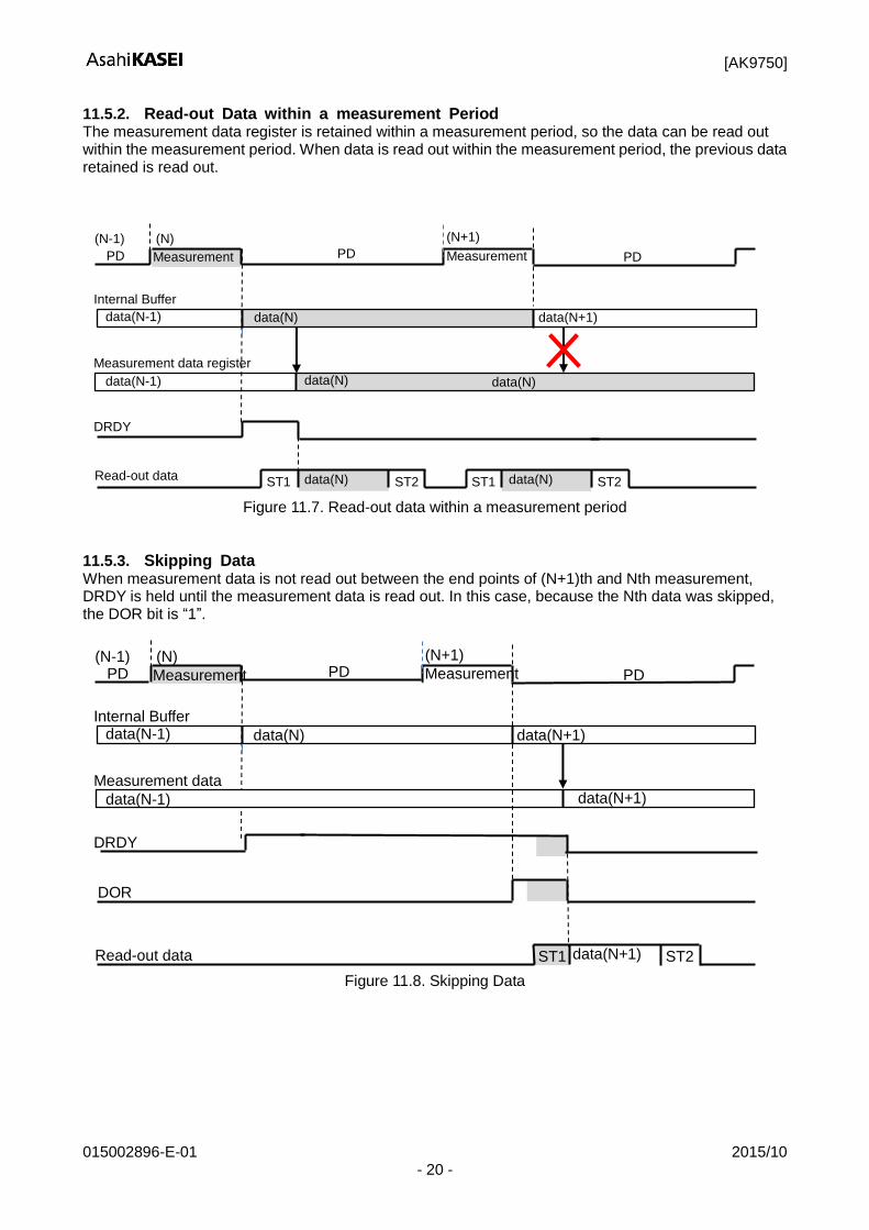
11.5.2. Read-out Data within a measurement Period The measurement data register is retained within a measurement period, so the data can be read out within the measurement period. When data is read out within the measurement period, the previous data retained is read out.
PD Measurement PD Measurement PD
(N) (N-1) (N+1)
Internal Buffer
data(N-1) data(N)
Measurement data register
data(N-1) data(N)
data(N+1)
DRDY
Read-out data ST1 data(N) ST2 ST1 data(N) ST2
data(N)
Figure 11.7. Read-out data within a measurement period
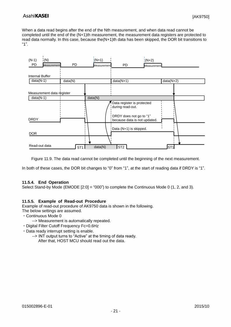
11.5.3. Skipping Data When measurement data is not read out between the end points of (N+1)th and Nth measurement, DRDY is held until the measurement data is read out. In this case, because the Nth data was skipped, the DOR bit is “1”.
PD Measurement PD Measurement PD
(N) (N-1) (N+1)
Internal Buffer data(N-1) data(N)
Measurement data
data(N-1) data(N+1)
data(N+1)
DRDY
Read-out data ST1 data(N+1) ST2
DOR
Figure 11.8. Skipping Data
[AK9750]
015002896-E-01 2015/10 - 21 -
When a data read begins after the end of the Nth measurement, and when data read cannot be completed until the end of the (N+1)th measurement, the measurement data registers are protected to read data normally. In this case, because the(N+1)th data has been skipped, the DOR bit transitions to “1”.
PD Measurement PD Measurement
(N) (N-1) (N+1)
Internal Buffer
data(N-1) data(N)
Measurement data register
data(N-1) data(N)
data(N+2)
DRDY
Read-out data ST1 data(N) ST2 ST1
PD Measurement
(N+2)
data(N+1)
Data (N+1) is skipped.
DOR
Data register is protected during read-out.
DRDY does not go to “1” because data is not updated.
Figure 11.9. The data read cannot be completed until the beginning of the next measurement.
In both of these cases, the DOR bit changes to “0” from “1”, at the start of reading data if DRDY is “1”.
11.5.4. End Operation Select Stand-by Mode (EMODE [2:0] = “000”) to complete the Continuous Mode 0 (1, 2, and 3).
11.5.5. Example of Read-out Procedure Example of read-out procedure of AK9750 data is shown in the following. The below settings are assumed.
・Continuous Mode 0
--> Measurement is automatically repeated.
・Digital Filter Cutoff Frequency Fc=0.6Hz
・Data ready interrupt setting is enable.
--> INT output turns to “Active” at the timing of data ready. After that, HOST MCU should read out the data.

[AK9750]
015002896-E-01 2015/10 - 22 -
Power On
Register Write (1) Soft Reset Address : 1DH Data : 01H (2) Mode and Fc setting Address : 1CH Data : 0CH (3) Interrupt Source setting Address : 1BH Data : 01H
Register Read (4) INT Status Address : 04H (5) Status1 Address : 05H (6) A/D Converted data of IR1 Address : 06H, 07H (7) A/D Converted data of IR2 Address : 08H, 09H (8) A/D Converted data of IR3 Address : 0AH, 0BH (9) A/D Converted data of IR4 Address : 0CH, 0DH (10) A/D Converted data of
Integrated Temperature Sensor Address : 0EH, 0FH (11) Status2 Address : 10H
INT output turns to “Active”
Wait Time 3.0 msec

[AK9750]
015002896-E-01 2015/10 - 23 -
12. Serial Interface
The I2C bus interface of the AK9750 supports Standard Mode (Max. 100kHz) and High Speed Mode
(Max. 400kHz).
12.1. Data Transfer Initially the start condition should be input to access the AK9750 through the bus. Next, send a one byte slave address, which includes the device address. The AK9750 compares the a¥slave address, and if these addresses match, the AK9750 generates an acknowledge signal and executes a Read / Write command. The stop condition should be input after executing a command.
12.1.1. Changing state of the SDA line The SDA line state should be changed only while the SCL line is “L”. The SDA line state must be maintained while the SCL line is “H”. The SDA line state can be changed while the SCL line is “H”, only when a Start Condition or a Stop Condition is input.
SCL
SDA
Constant Changing Stare Enable
Figure 12.1.Changing state of SDA line
12.1.2. Start / Stop Conditions A Start Condition is generated when the SDA line state is changed from “H” to “L” while the SCL line is “H”. All command start from a Start condition. A Stop condition is generated when the SDA line state is changed from “L” to “H” while the SCL line is “H”. All command end after a Stop condition.
SCL
SDA
Start Condition Stop Condition
Figure 12.2. Start / Stop Conditions

[AK9750]
015002896-E-01 2015/10 - 24 -
12.1.3. Acknowledge The device transmitting data will release the SDA line after transmitting one byte of data (SDA line state is “H”). The device receiving data will pull the SDA line to “L” during the next clock. This operation is called “Acknowledge”. The Acknowledge signal can be used to indicate successful data transfers. The AK9750 will output an acknowledge signal after receiving a Start condition and Slave address. The AK9750 will output an acknowledge signal after receiving each byte, when the WRITE instruction is transmitted. The AK9750 will transmit the data stored in the selected address after outputting an acknowledge signal, when a READ instruction is transmitted. Then the AK9750 will monitor the SDA line after releasing the SDA line. If the master device generates an Acknowledge instead of Stop condition, the AK9750 transmits an 8-bit data stored in the next address. When the Acknowledge is not generated, transmitting data is terminated.
SCL of Master Device.
Data Output of Transmitter
Data Output of Receiver
Start Condition
1 8 9
Clocl pulse for Acknowledge
Non-Acknowledge
Acknowledge
Figure 12.3. Acknowledge

[AK9750]
015002896-E-01 2015/10 - 25 -
12.1.4. Slave Address The Slave address of the AK9750 can be selected from the following list by setting the CAD0/1 pins. When the CAD0/1 pins are connected to VSS, the Slave address bit is = “0”. When the CAD0/1 pins are connected to VDD, the Slave address bit is “1”. Do not set up “CAD1 pin = CAD0 pin = 1” while the I
2C
interface is used, because the “CAD1 pin = CAD0 pin = 1” state is only for Switch Mode.
Table 12.1. CAD0/1 pin setting and Slave Address
CAD1 pin CAD0 pin Slave Address
0 0 64H
0 1 65H
1 0 66H
1 1 Switch Mode
When the first one byte data including the Slave address is transmitted after a Start condition, the device, which is specified as the communicator by the Slave address on bus, selected. After transmitting the Slave address, the device that has the corresponding device address will execute a command after transmitting an Acknowledge signal. The 8-bit (Least Significant bit-LSB) of the first one byte is the R/W bit. When the R/W bit is set to “1”, a READ command is executed. When the R/W bit is set to “0”, a WRITE command is executed. MSB LSB
1 1 0 0 1 CAD1 CAD0 R/W
Figure 12.4. Slave Address

[AK9750]
015002896-E-01 2015/10 - 26 -
12.1.5. WRITE Command When the R/w bit set to “0”, the AK9750 executes a WRITE Operation. The AK9750 will out an Acknowledge signal and receive the second byte, after receiving a Start condition and first one byte (Slave address) in a WRITE Operation. The second byte has an MSB-first configuration, and specifies the address of the internal control register.
MSB LSB
A7 A6 A5 A4 A3 A2 A1 A0
Figure 12.5. Register Address The AK9750 will generate an Acknowledge and receive the third byte after receiving the second byte (Register Address). The data after the third byte is the control data. The control data consists of 8-bit and has an MSB-first configuration. The AL9750 generates an Acknowledge for each byte received. The data transfer is terminated by a Stop condition, generated by the master device. MSB LSB
D7 D6 D5 D4 D3 D2 D1 D0
Figure 12.6. Control data Two or more bytes can be written at once. The AK9750 generates an Acknowledge and receives the next data after receiving the third byte (Control Data). When the following data is transmitted without a Stop condition, after transmitting one byte, the internal address counter is automatically incremented, and data is written in the next address. The automatic increment function works in the address from 11H to 1CH.Wthen the start address is “11H”, the address is repeatedly incremented as. “11H -> 12H ->…..-> 1CH -> 11H -> 12H…”
SDA S Slave Address
R/W= 0
AC
K
Register Address(n)
AC
K
DATA(n) DATA(n+1) DATA(n+x) P
Sta
rt
Sto
p
AC
K
AC
K
AC
K
AC
K
Figure 12.7. WRITE Operation

[AK9750]
015002896-E-01 2015/10 - 27 -
12.1.6. READ Command When the R/W bit is set to “1”, the AK9750 executes a READ Operation. When the AK9750 transmits data from the specified address, the master device generates an Acknowledge instead of a Stop condition and the next address data can be read out. The AK9750 supports both current address read and random address read. The automatic increment function works in the address of 05H to 10H. When the address 10H is read out, the next address returns to 05H. (1) Current Address Read The AK9750 has an integrated address counter. The data specified by the counter is read out in the current address read operation. The internal address counter retains the next address which is accessed at last. For example, when the address which was accessed last is “n”, the data of address “n+1” is read out by the current address read instruction. The AK9750 will generate an Acknowledge after receiving a Slave address for a Read command (R/W bit = “1”) in the current address read operation. Then the AK9750 will start to transmit the data specified by the internal address counter at the next clock, and will increment the internal address counter by one. When the AK9750 generates a Stop condition instead of an Acknowledge after transmitting the one byte data, a Read out operation is terminated.
SDA S Slave Address
R/W= “1”
AC
K
AC
K
DATA(n) DATA(n+2) DATA(n+x) P
Sta
rt
Sto
p
AC
K
AC
K
AC
K
AC
K
DATA(n+1)
Figure 12.8. Current Address Read
(2) Random Read Data from an arbitrary address can be read out by a random read operation. A random read requires the input of a dummy WRITE instruction before the input of a slave address of a RED instruction (R/W bit = “1”). To execute a random read, first generate a start condition, then input the slave address for a WRITE instruction (R/W bit = “0”) and a read address, sequentially. After the AK9750 generates an Acknowledge in response to this address input, generate a start condition and the slave address for a READ instruction (R/W)R/W bit = “1”) again. The AK9750 generates an Acknowledge in response to the input of this slave address. Next, the AK9750 output the data at the specified address, then increments the internal address counter by one. When a Stop condition from the master device is generated in generated instead of an Acknowledge after the AK9750 outputs data, Read operation stops.
SDA S Slave Address
R/W= “0”
AC
K
AC
K
DATA(n) DATA(n+x) P
Sta
rt
Sto
p
AC
K
AC
K
AC
K
AC
K
DATA(n+1) Register Address(n)
Slave Address
S
R/W= “1”
Sta
rt
Figure 12.9. Random Read

[AK9750]
015002896-E-01 2015/10 - 28 -
12.1.7. EEPROM Write Timing Writing data to EEPROM should be done at shown timing as the following.
tWR ≥ 10ms
SCL
SDA 8th bit
WORD n
ACK STOP START
SDA S Slave Address
R/W= “0”
AC
K
AC
K
DATA EKEY Register Address
P
Sta
rt
Sto
p
AC
K
AC
K
AC
K
EMODE Register Address
AC
K
Data Slave Address
S
R/W= “0”
Sta
rt
P
Sto
p
Slave Address
R/W= “0”
Sta
rt
S EEPROM Address
AC
K
DATA
AC
K
AC
K
S
Sta
rt
P
Sto
p
tWR ≥ 10ms
Figure 12.10. EEPROM Write Timing
Writing data to EEPROM should be done as the sequence that is shown in Figure 12.10. Writing data to EEPROM can be done after setting EMODE [2:0] = “001”, EEPMODE = “1” and EKEY [7:0] = “A5H”. Writing data to EEPROM is started at the Stop Condition after inputting the data, and terminated at the Start Condition. EEPROM write time (tWR) should be longer than 10ms. Two or more bytes cannot be written at once in writing data to EEPROM should be done after setting EKEY [7:0] = “A5H” again. On the other hand, reading data from EEPROM is able to be continuously done.

[AK9750]
015002896-E-01 2015/10 - 29 -
13. Memory Map
Table 13.1. Register Map
Name Address Soft Reset R/W Data
Content bit
WIA1 00H Disable R Company Code 8
WIA2 01H Disable R Device ID 8
INFO1 02H Disable R Information 8
INFO2 03H Disable R Information 8
INTST 04h Enable R Interrupt Status 3
ST1 05H Enable R Status 1 2
IR1L 06H Enable R IR1 A/D Converted data (Low) 8
IR1H 07H Enable R IR1 A/D Converted data (High) 8
IR2L 08H Enable R IR2 A/D Converted data (Low) 8
IR2H 09H Enable R IR2 A/D Converted data (High) 8
IR3L 0AH Enable R IR3 A/D Converted data (Low) 8
IR3H 0BH Enable R IR3 A/D Converted data (High) 8
IR4L 0CH Enable R IR4 A/D Converted data (Low) 8
IR4H 0DH Enable R IR4 A/D Converted data (High) 8
TMPL 0EH Enable R Integrated Temperature Sensor Output (Low) 8
TMPH 0FH Enable R Integrated Temperature Sensor Output (High) 8
ST2 10H Disable R Status 2 (dummy) -
ETH13H 11H Enable R/W IR1 – IR3 Upper Threshold level (Low) 6
ETH13H 12H Enable R/W IR1 – IR3 Upper Threshold level (High) 6
ETH13L 13H Enable R/W IR1 – IR3 Lower Threshold level (low) 6
ETH13L 14H Enable R/W IR1 – IR3 Lower Threshold level (High) 6
ETH24H 15H Enable R/W IR2 – IR4 Upper Threshold level (Low) 6
ETH24H 16H Enable R/W IR2 – IR4 Upper Threshold level (High) 6
ETH24L 17H Enable R/W IR2 – IR4 Lower Threshold level (Low) 6
ETH24L 18H Enable R/W IR2 – IR4 Lower Threshold Level (High) 6
EHYS13 19H Enable R/W IR1 – IR3 Hysteresis of Threshold 5
EHYS24 1AH Enable R/W IR2 – IR4 Hysteresis of Threshold 5
EINTEN 1BH Enable R/W Interrupt Source Setting 5
ECNTL1 1CH Enable R/W Mode Setting
Fc Setting 7
CNTL2 1DH Enable R/W Soft Reset 3
Note: * 12. When Switch Mode (CAD1 = CAD0 = “H”) is selected, “ETH13H to ECNTL1” of registers data (Address 11H to 1CH) copies “ETH13H to ECNTL1” of EEPROM data (Address 51H to 5CH).

[AK9750]
015002896-E-01 2015/10 - 30 -
Table 13.2. EEPROM Map
Name Address R/W Data
Content bit
EKEY 50H R/W EEPROM Access key (* 13) 8
ETH13H 51H R/W IR1 – IR3 Upper Threshold level (Low) 6
ETH13H 52H R/W IR1 – IR3 Upper Threshold level (High) 6
ETH13L 53H R/W IR1 – IR3 Lower Threshold level (Low) 6
ETH13L 54H R/W IR1 – IR3 Lower Threshold level (High) 6
ETH24H 55H R/W IR2 – IR4 Upper Threshold level (Low) 6
ETH24H 56H R/W IR2 – IR4 Upper Threshold level (High) 6
ETH24L 57H R/W IR2 – IR4 Lower Threshold level (Low) 6
ETH24L 58H R/W IR2 – IR4 Lower Threshold level (High) 6
EHYS13 59H R/W IR1 – IR3 Hysteresis of Threshold 5
EHYS24 5AH R/W IR2 – IR4 Hysteresis of Threshold 5
EINTEN 5BH R/W Interrupt Factor Setting 5
ECNTL1 5CH R/W Mode Setting
Fc Setting 7
Note: * 13. EKEY is registers. When EEPROM Access Mode (EMODE [2:0] bits = “001” and EEPMODE bit = “1”) is selected, EEPROM can be written by setting EKEY [7:0] bits = “A5H”.

[AK9750]
015002896-E-01 2015/10 - 31 -
14. Registers Functional Descriptions
Table 14.1. Register Detail Map
Address Name D7 D6 D5 D4 D3 D2 D1 D0
00H WIA1 0 1 0 0 1 0 0 0
01H WIA2 0 0 0 1 0 0 1 1
02H INFO1 0 0 0 0 0 0 0 0
03H INFO2 0 0 0 0 0 0 0 0
04H INTST 1 1 1 IR13H IR13L IR24H IR24L DR
05H ST1 1 1 1 1 1 1 DOR DRDY
06H IR1L IR1_7 IR1_6 IR1_5 IR1_4 IR1_3 IR1_2 IR1_1 IR1_0
07H IR1H IR1_15 IR1_14 IR1_13 IR1_12 IR1_11 IR1_10 IR1_9 IR1_8
08H IR2L IR2_7 IR2_6 IR2_5 IR2_4 IR2_3 IR2_2 IR2_1 IR2_0
09H IR2H IR2_15 IR2_14 IR2_13 IR2_12 IR2_11 IR2_10 IR2_9 IR2_8
0AH IR3L IR3_7 IR3_6 IR3_5 IR3_4 IR3_3 IR3_2 IR3_1 IR3_0
0BH IR3H IR3_15 IR3_14 IR3_13 IR3_12 IR3_11 IR3_10 IR3_9 IR3_8
0CH IR4L IR4_7 IR4_6 IR4_5 IR3_4 IR4_3 IR4_2 IR4_1 IR4_0
0DH IR4H IR4_15 IR4_14 IR4_13 IR4_12 IR4_11 IR4_10 IR4_9 IR4_8
0EH TMPL TMP_7 TMP_6 TMP_5 TMP_4 TMP_3 TMP_2 TMP_1 TMP_0
0FH TMPH TMP_15 TMP_14 TMP_13 TMP_12 TMP_11 TMP_10 TMP_9 TMP_8
10H ST2 1 1 1 1 1 1 1 1
11H ETH13H ETH13H_4 ETH13H_3 ETH13H_2 ETH13H_1 ETH13H_0 0 0 0
12H ETH13H 0 ETH13H_11 ETH13H_10 ETH13H_9 ETH13H_8 ETH13H_7 ETH13H_6 ETH13H_5
13H ETH13L ETH13L_4 ETH13L_3 ETH13L_2 ETH13L_1 ETH13L_0 0 0 0
14H ETH13L 0 ETH13L_11 ETH13L_10 ETH13L_9 ETH13L_8 ETH13L_7 ETH13L_6 ETH13L_5
15H ETH24H ETH24H_4 ETH24H_3 ETH24H_2 ETH24H_1 ETH24H_0 0 0 0
16H ETH24H 0 ETH24H_11 ETH24H_10 ETH24H_9 ETH24H_8 ETH24H_7 ETH24H_6 ETH24H_5
17H ETH24L ETH24L_4 ETH24L_3 ETH24L_2 ETH24L_1 ETH24L_0 0 0 0
18H ETH24L 0 ETH24L_11 ETH24L_10 ETH24L_9 ETH24L_8 ETH24L_7 ETH24L_6 ETH24L_5
19H EHYS13 1 1 1 EHYS13_4 EHYS13_3 EHYS13_2 EHYS13_1 EHYS13_0
1AH EHYS24 1 1 1 EHYS24_4 EHYS24_3 EHYS24_2 EHYS24_1 EHYS24_0
1BH EINTEN 1 1 0 IR13HI IR13LI IR24HI IR24LI DRI
1CH ECNTL1 1 EEPMODE EFC_2 EFC_1 EFC_0 EMODE_2 EMODE_1 EMODE_0
1DH CNTL2 1 1 1 1 1 1 1 SRST
[Functional Descriptions] 1). WIA1: Company Code (Read Only Registers)
Address Name D7 D6 D5 D4 D3 D2 D1 D0
00H WIA1 0 1 0 0 1 0 0 0
1 Byte fixed code as Company code of AKM. 2). WIA2: Device ID (Read Only Registers)
Address Name D7 D6 D5 D4 D3 D2 D1 D0
01H WIA2 0 0 0 1 0 0 1 1
1 Byte fixed code as AKM device ID.

[AK9750]
015002896-E-01 2015/10 - 32 -
3). INFO1: Information (Read Only Registers)
Address Name D7 D6 D5 D4 D3 D2 D1 D0
02H INFO1 0 0 0 0 0 0 0 1
INFO1 [7:0]: Information for AKM use only. 4). INFO2: Information (Read Only Registers)
Address Name D7 D6 D5 D4 D3 D2 D1 D0
03H INFO2 0 0 0 0 0 0 0 0
INFO2 [7:0]: Reserve 5). INTST: Interrupt Status (Read Only Registers)
Address Name D7 D6 D5 D4 D3 D2 D1 D0
04H INTST IR13H IR13L IR24H IR24L DR
Reset 1 1 1 0 0 0 0 0
When the correspondent bit in the Interrupt Source Register (EINTEN) is enabled, the interrupt to the host MCU is available. When the interruption happens, the interrupt source is confirmed by reading the interrupt status register. When INST register is read out, INT pin turns to “non-active”. This register is rest, when the differential signal of two IR sensors (IR1 - IR3 / IR2 - IR4) are below “the upper threshold levels - hysteresis” or the differential signal of two IR sensors (IR1 - IR3 / IR2 – IR4) are above “the lower threshold levels + hysteresis” or the software reset is done or Write accessing to ECNTL1 register is done. DR: Data Ready “0”: Normal state “1”: Data Ready DR bit goes “1”, when the data is ready with DRI bit = “1” IR13H / IR24H: The differential signals of two IR sensors (IR1 - IR3 / IR2 - IR4) are equal to or above the upper threshold levels. “0”: The differential signals (IR1 – IR3/IR2 – IR4) are below the upper threshold levels. “1”: The differential signals (IR1 – IR3/IR2 – IR4) are below the upper threshold levels. When IR13H / IR24HI bit is set to “1” in the interrupt source registers(EINTEN), IR13H / IR24H bit turns to “1”, when the differential signals (IR1 - IR3 / IR2 - IR4) are equal to or above the upper threshold levels which are set in ETH13 / ETH24H registers. Otherwise it stays at “0”. IR13L / IR24L: The differential signals of two IR sensors (IR1 - IR3 / IR2 - IR4) are equal to or below the lower threshold levels. “0”: The differential signals (IR1 - IR3 / IR2 - IR4) are above the lower threshold levels. “1”: The differential signals (IR1 - IR3 / IR2 - IR4) are equal to or below the lower threshold levels. When IR13LI / IR24LI bit set to “1” in the interrupt source registers (EINTEN), IR13L / IR24L bit turns to “1”, when the differential signals (IR1 - IR3 / IR2 - IR4) are equal to or below the lower threshold levels which are set in ETH13L / ETH24L registers. Otherwise it stays at “0”.

[AK9750]
015002896-E-01 2015/10 - 33 -
6). ST1: Status 1 (Read Only Registers)
Address Name D7 D6 D5 D4 D3 D2 D1 D0
05H ST1 DOR DRDY
Reset 1 1 1 1 1 1 0 0
DRDY: Data Ready “0”: Normal State “1”: Data Ready The DRDY bit turns to “1”, when the data is ready to be read. This bit turns back to “0”, when either the ST2 register or one of the measured data (IRS1L to TMPH) is read. DOR: Data Overrun “0”: Normal State “1”: Data Overrun The DOR bit turns to “1”, when the data reading is skipped. This bit turns back to “0”, when either the ST2 register or one of the measured data (IRS1L to TMPH) is read.

[AK9750]
015002896-E-01 2015/10 - 34 -
7). IRxL, IRxH: Measurement Data of IR sensor (x= 1, 2, 3, 4) (Read Only Registers)
Address Name D7 D6 D5 D4 D3 D2 D1 D0
06,08,0A,0C H IRxL IRxL_7 IRxL_6 IRxL_5 IRxL_4 IRxL_3 IRxL_2 IRxL_1 IRxL_0
07,09,0B,0D H IRxH IRxH_15 IRxH_14 IRxH_13 IRxH_12 IRxH_11 IRxH_10 IRxH_9 IRxH_8
Reset 0 0 0 0 0 0 0 0
Measurement Data of IR sensor IRxL [7:0]: Least significant 8-bits in output data IRxH [15:8]: Most significant 8-bits in output data 16-bit data is stored in tow’s compliment format.
Table 14.2. Measurement Data of IR sensor
Measurement Data IR Sensor [15:0] Output Current of IR Sensor Unit
Two’s Complement Hex Decimal
0111 1111 1111 1111 7FFF 32767 14286.4
pA
⁞ ⁞ ⁞ ⁞
0101 1001 1001 1000 5998 22936 10000.1
⁞ ⁞ ⁞ ⁞
0100 0000 1000 0010 4082 16514 7000.1
⁞ ⁞ ⁞ ⁞
0000 1000 1111 0110 08F6 2294 1000.2
⁞ ⁞ ⁞ ⁞
0000 0000 0010 0000 0020 32 14.0
⁞ ⁞ ⁞ ⁞
0000 0000 0000 0000 0000 0 0
⁞ ⁞ ⁞ ⁞
1111 1111 1110 0000 FFE0 -31 13.5
⁞ ⁞ ⁞ ⁞
1111 0111 0000 1001 F709 -2294 -1000.2
⁞ ⁞ ⁞ ⁞
1011 1111 0111 1101 BF7D -16514 -7200.1
⁞ ⁞ ⁞ ⁞
1010 0110 0110 0111 9667 -22936 -10000.1
⁞ ⁞ ⁞ ⁞
1000 0000 0000 0000 8000 -32768 -14286.8
Note: * 14. When the digital filter cutoff frequency is set to Fc= 1.1Hz, the output current under 15.8pA cannot
be measured by the noise.
[AK9750]
015002896-E-01 2015/10 - 35 -
8). TMPL, TMPH: Measurement Data of the Integrated temperature Sensor (Read / Write Registers)
Address Name D7 D6 D5 D4 D3 D2 D1 D0
0EH TMPL TMPL_7 TMPL_6 TMPL_5 TMPL_4 TMPL_3 TMPL_2 TMPL_1 TMPL_0
0FH TMPH TMPH_15 TMPH_14 TMPH_13 TMPH_12 TMPH_11 TMPH_10 TMPH_9 TMPH_8
Reset 0 0 0 0 0 0 0 0
Note: * 15. TMPL_0 bit to TMPL_5 bit are fixed to “0”. Measurement Data of the Integrated Temperature Sensor TMPL [7:0]: Least significant 8-bits in output data TMPH [15:8]: Most significant 8-bits in output data 16-bit data is stored in tow’s compliment format.
Table 14.3. Measurement Data of the Integrated Temperature Sensor
Measurement Data of the Integrated Temperature Sensor [15:0] Temperature Unit
Two’s Complement Hex Decimal
0100 0011 1000 0000 4380 17792 60
ºC
⁞ ⁞ ⁞ ⁞
0000 0001 0000 0000 0100 256 26.75+0.5
⁞ ⁞ ⁞ ⁞
0000 0000 0100 0000 0040 64 26.75+0.125
0000 0000 0000 0000 0000 0 26.75
1111 1111 1100 0000 FFC0 -64 26.75-0.125
⁞ ⁞ ⁞ ⁞
1111 1111 0000 0000 FF00 -256 26.75-0.5
⁞ ⁞ ⁞ ⁞
1011 1001 1000 0000 B980 -18048 -10
The Resolution of the Integrated Temperature Sensor
Table 14.4. The Resolution of the Integrated Temperature Sensor
EFC[2:0] Setting EFC= All Setting
Resolution 10-bit (0.125ºC)
9). ST2: Status 2 (Read Only Registers)
Address Name D7 D6 D5 D4 D3 D2 D1 D0
10H ST2
Reset 1 1 1 1 1 1 1 1
Note: * 16. ST2 register is the dummy data register for the measured data reading routine.ST2 register MUST
be read after reading out the measured data.

[AK9750]
015002896-E-01 2015/10 - 36 -
10). ETH13H, ETH24H, ETH12L, ETH24L: Threshold level setting for the differential outputs (IR1 - IR3 / IR2 - IR4) (Read / Write Registers)
Address Name D7 D6 D5 D4 D3 D2 D1 D0
11H ETH13H TEH13H_4 TEH13H_3 ETH13H_2 ETH13H_1 ETH13H_0 0 0 0
12H ETH13H 0 ETH13H_11 ETH13H_10 ETH13H_9 ETH13H_8 ETH13H_7 ETH13H_6 ETH13H_5
13H ETH13L ETH13L_4 ETH13L_3 ETH13L_2 ETH13L_1 ETH13L_0 0 0 0
14H ETH13L 0 ETH13L_11 ETH13L_10 ETH13L_9 ETH13L_8 ETH13L_7 ETH13L_6 ETH13L_5
15H ETH24H ETH24H_4 ETH24H_3 ETH24H_2 ETH24H_1 ETH24H_0 0 0 0
16H ETH24H 0 ETH24H_11 ETH24H_10 ETH24_9 ETH24H_8 ETH24H_7 ETH24H_6 ETH24H_5
17H ETH24L ETH24L_4 ETH24L_3 ETH24L_2 ETH24L_1 ETH24L_0 0 0 0
18H ETH24L 0 ETH24L_11 ETH24L_10 ETH24L_9 ETH24L_8 ETH24L_7 ETH24L_6 ETH13L_5
Reset 0 0 0 0 0 0 0 0
Threshold Level setting for the differential output (IR1 - IR3 / IR2 - IR4) TH13H [11:0], TH24H [11:0]: Upper Threshold Level setting for the differential output (IR1 - IR3 / IR2 - IR4) TH13L [11:0], TH24L [11:0]: Lower Threshold Level setting for the differential output (IR1 - IR3 / IR2 - IR4)
The setting range is shown in Table 14.5.
Table 14.5. Threshold Level setting for the differential output (IR1 - IR3 / IR2 - IR4)
Threshold level [11:0] Differential Current Output Unit
Two’s Complement Hex Decimal
0111 1111 1111 7FF 2047 7139.32
pA
⁞ ⁞ ⁞ ⁞
0000 0000 0001 001 1 3.4877
0000 0000 0000 000 0 0
1111 1111 1111 FFF -3.4877
⁞ ⁞ ⁞ ⁞
1000 0000 0000 800 -2048 -7142.81
Differential current output is calculated by the following formula,
Differential current output = 3.4877 x Threshold level [11:0](Decimal) pA Note:
* 17. The threshold levels should be set as “ETH13H > ETH13L, ETH24H > ETH24L”. Otherwise, AK9750
cannot operate normally.

[AK9750]
015002896-E-01 2015/10 - 37 -
11). EHYS13, EHYS24: Hysteresis setting of Threshold Level / Polarity setting of INT output. (Read / Write Registers)
Address Name D7 D6 D5 D4 D3 D2 D1 D0
19H EHYS13 EHYS13_4 EHYS13_3 EHYS13_2 EHYS13_1 EHYS13_0
1AH EHYS24 EHYS24_4 EHYS24_3 EHYS24_2 EHYS24_1 EHYS24_0
Reset 1 1 1 0 0 0 0 0
Hysteresis setting for Threshold levels ETHYS13, EHYS24: Hysteresis setting for threshold levels 5-bit This register is used only in Switch Mode (ECOPY).
Table 14.6. Hysteresis setting of Threshold Level
Hysteresis [4:0] Differential Current Output Unit
Binary Hex Decimal
11111 1F 31 108.12
pA
11110 1E 30 104.63
⁞ ⁞ ⁞ ⁞
00001 01 1 3.4877
00000 00 0 0
The relationship between the hysteresis and the threshold level is shown in Figure 14.1.
INT Output
“H” Level
“L” Level
EHYS13
or
EHYS24
EHYS13
or
EHYS24
The Differential Output (IR1 - IR3 / IR2 - IR4)
Figure 14.1. Hysteresis setting for threshold levels.
Detection is defined as the situation in which the differential output (IR1 - IR3 / IR2 - IR4) exceeds the threshold level.
[AK9750]
015002896-E-01 2015/10 - 38 -
12). EINTEN: Interrupt Source setting (Read / Write Registers)
Address Name D7 D6 D5 D4 D3 D2 D1 D0
1BH EINTEN IR13HI IR13LI IR24HI IR24LI DRI
Reset 1 1 0 0 0 0 0 0
The interrupt to the HOST MCU via the INT output can be obtained by the following methods: INT output turns to “Active”, when at least one of the enabled interrupt source conditions is satisfied. HOST MCU can identify the interrupt source by reading the Interrupt Source Status (INST). When DRI and threshold Level interrupt (IR13HI, IR13LI, IR24HI and IR24LI) are simultaneously set to “Enable”, the priority is given to threshold level interrupt. DRI: Data ready interrupt setting “0”: Interrupt Disable “1”: Interrupt Enable Setting DRI bit to “1” enables the interrupt function at the timing of data ready. IR13HI / IR24HI: Upper threshold level interrupt setting “0”: Interrupt Disable “1”: Interrupt Enable Setting IR13H / IR24HI bit to “1” enables the interrupt function at the timing in which the differential output (IR1 - IR3 / IR2 - IR4) changes from the level which is below the upper threshold level to the level which is above the upper threshold level, or at the timing in which the differential output (IR1 - IR3 / IR2 - IR4) changes from the level which is above “the upper threshold level - hysteresis” to the level which is below “the upper threshold level - hysteresis”. IR13LI / IR24LI: Lower threshold level interrupt setting. “0”: Interrupt Disable “1”: Interrupt Enable Setting IR13LI/IR24LI bit to “1” enables the interrupt function at the timing in which the differential output (IR1 - IR3 / IR2 - IE4) changes from the level which is above the lower threshold level to the level which is below the lower threshold level, or at the timing in which the differential output (IR1 - IR3 / IR2 - IR4) changes from the level which is below “the lower threshold level +hysteresis” to the level which is above “the lower threshold level +hysteresis.

[AK9750]
015002896-E-01 2015/10 - 39 -
13). ECNTL1: Mode setting/ Digital Filter Cutoff Frequency (Fc) setting (Read / Write registers)
Address Name D7 D6 D5 D4 D3 D2 D1 D0
1CH ECNTL1 EEPMODE EFC_2 EFC_1 EFC_0 EMODE_2 EMODE_1 EMODE_0
Reset 1 0 0 0 0 0 0 0
EMODE [2:0]: Mode setting “000”: Stand-by Mode “001”: EEPROM Access Mode (EEPMODE bit should be set to “1” simultaneously) “010”: Shingle Shot Mode “011”: Be prohibited “100”: Continuous Mode 0 (Normal operation) “101”: Continuous Mode 1 (Intermittent operation => Measurement time: Wait time = 1:1) “110”: Continuous Mode 2 (Intermittent operation => Measurement time: Wait time = 1:3) “111”: Continuous Mode 3 (Intermittent operation => Measurement time: Wait time = 1:7) EFC [2:0]: Digital Filter Cutoff Frequency (Fc) setting “000”: Fc = 0.3Hz “001”: Fc = 0.6Hz “010”: Fc = 1.1Hz “011”: Fc = 2.2Hz “100”: Fc = 4.4Hz “101”: Fc = 8.8Hz “11x”: Be prohibited The digital filter is “sinc function” type. The Fc is defined as the frequency at which Gain is -3dB. EEPMODE Setting “0”: Normal Mode “1”: EEPROM Access Mode (EMODE [2:0] bits should be set to “001” simultaneously) 14). CNTL2: Soft Reset (Read / Write Registers)
Address Name D7 D6 D5 D4 D3 D2 D1 D0
1DH CNTL2 SRST
Reset 1 1 1 1 1 1 1 0
SRST: Soft Reset “0”: Normal State “1”: Reset All registers are reset by setting SRST bit to “1”. SRST bit automatically returns to “0” after reset is activated.
[AK9750]
015002896-E-01 2015/10 - 40 -
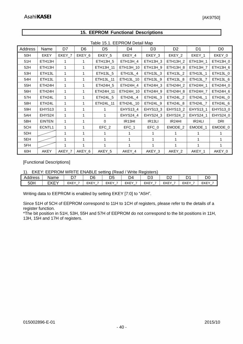
15. EEPROM Functional Descriptions
Table 15.1. EEPROM Detail Map
Address Name D7 D6 D5 D4 D3 D2 D1 D0
50H EKEY EKEY_7 EKEY_6 EKEY_5 EKEY_4 EKEY_3 EKEY_2 EKEY_1 EKEY_0
51H ETH13H 1 1 ETH13H_5 ETH13H_4 ETH13H_3 ETH13H_2 ETH13H_1 ETH13H_0
52H ETH13H 1 1 ETH13H_11 ETH13H_10 ETH13H_9 ETH13H_8 ETH13H_7 ETH13H_6
53H ETH13L 1 1 ETH13L_5 ETH13L_4 ETH13L_3 ETH13L_2 ETH13L_1 ETH13L_0
54H ETH13L 1 1 ETH13L_11 ETH13L_10 ETH13L_9 ETH13L_8 ETH13L_7 ETH13L_6
55H ETH24H 1 1 ETH24H_5 ETH24H_4 ETH24H_3 ETH24H_2 ETH24H_1 ETH24H_0
56H ETH24H 1 1 ETH24H_11 ETH24H_10 ETH24H_9 ETH24H_8 ETH24H_7 ETH24H_6
57H ETH24L 1 1 ETH24L_5 ETH24L_4 ETH24L_3 ETH24L_2 ETH24L_1 ETH24L_0
58H ETH24L 1 1 ETH24L_11 ETH24L_10 ETH24L_9 ETH24L_8 ETH24L_7 ETH24L_6
59H EHYS13 1 1 1 EHYS13_4 EHYS13_3 EHYS13_2 EHYS13_1 EHYS13_0
5AH EHYS24 1 1 1 EHYS24_4 EHYS24_3 EHYS24_2 EHYS24_1 EHYS24_0
5BH EINTEN 1 1 0 IR13HI IR13LI IR24HI IR24LI DRI
5CH ECNTL1 1 1 EFC_2 EFC_1 EFC_0 EMODE_2 EMODE_1 EMODE_0
5DH 1 1 1 1 1 1 1 1
5EH 1 1 1 1 1 1 1 1
5FH 1 1 1 1 1 1 1 1
60H AKEY AKEY_7 AKEY_6 AKEY_5 AKEY_4 AKEY_3 AKEY_2 AKEY_1 AKEY_0
[Functional Descriptions] 1). EKEY: EEPROM WRITE ENABLE setting (Read / Write Registers)
Address Name D7 D6 D5 D4 D3 D2 D1 D0
50H EKEY EKEY_7 EKEY_7 EKEY_7 EKEY_7 EKEY_7 EKEY_7 EKEY_7 EKEY_7
Writing data to EEPROM is enabled by setting EKEY [7:0] to “A5H”. Since 51H of 5CH of EEPROM correspond to 11H to 1CH of registers, please refer to the details of a register function. *The bit position in 51H, 53H, 55H and 57H of EEPROM do not correspond to the bit positions in 11H, 13H, 15H and 17H of registers.

[AK9750]
015002896-E-01 2015/10 - 41 -
16. First data Determination Time
The First data determination time is defined as the time between “setting the registers” and “determining the measurement data”. It depends on Measurement Mode setting and Digital Filter setting. Since the first data determination time also depends on the OCS frequency, Min./Max. is Typ. ±10%. <First data Determination Time (Typ.) in each Measurement Mode>
Table 16.1. First data Determination Time
EFC [2:0] Unit
EMODE [2:0] EFC= “0H” EFC= “1H” EFC= “2H” EFC= “3H” EFC= “4H” EFC= “5H”
Single Shot Mode 2.309 1.157 0.581 0.293 0.149 0.077
sec
Continuous Node0 2.309 1.157 0.581 0.293 0.149 0.077
Continuous Mode1 2.309 1.157 0.581 0.293 0.149 0.077
Continuous Mode2 2.309 1.157 0.581 0.293 0.149 0.077
Continuous Mode3 2.309 1.157 0.581 0.293 0.149 0.077
Note: * 18. In Switch Mode, the first data determination time is defined as the time between “Power on Reset
and determining INT output measurement data”. The first data determination time is 0.02 second longer than time shown in Table 16.1, in Switch Mode.
17. Data Sampling Period
The data sampling period is defined as the time in which AK9750 updates an IR measurement data periodically after determining the first data. The data sampling period depends on Measurement Mode setting and Digital Filter setting. Since the data sampling period also depends on the OCS frequency, Min / Max. is Typ. ±10%. <Data Sampling Period of IR Sensor in each Measurement Mode>
Table 17.1. Data Sampling Period (Typ.) of IR Sensor
EFC [2:0] Unit
EMODE [2:0] EFC= “0H” EFC= “1H” EFC= “2H” EFC= “3H” EFC= “4H” EFC= “5H”
Continuous Mode 0 0.576 0.288 0.144 0.072 0.036 0.018
sec Continuous Mode 1 4.608 2.304 1.152 0.576 0.288 0.144
Continuous Mode 2 9.216 4.608 2.304 1.152 0.576 0.288
Continuous Mode 3 18.432 9.216 4.608 2.304 1.152 0.576
<Data Sampling Period of Temperature Sensor data in each Measurement Mode> The data sampling period of the temperature sensor is changed by changing EMODE [2:0] as shown in Table 17.2. The data sampling period of the temperature sensor does not depend on the digital filter setting (EFC [2:0]).
Table 17.2. Data Sampling Period (Typ.) of Temperature Sensor
EMODE [2:0] Period Unit
Continuous Mode 0 0.576
sec Continuous Mode 1 4.608
Continuous Mode 2 9.216
Continuous Mode 3 18.432

[AK9750]
015002896-E-01 2015/10 - 42 -
18. Sensor’s Output (Reference)
Ts: Sensor Temperature Ttgt: Target Temperature
Figure 18.1. IR Output
19. Spectrum Sensitivity (Reference)
Figure 19.1. Spectrum Sensitivity
<Measurement Conditions> Sensor Temperature Ts= 25ºC (298K)

[AK9750]
015002896-E-01 2015/10 - 43 -
20. Field of View (Reference)
Parameter Symbol Min. Typ. Max. Unit
Field of View (* 19) FOV ±48 ±55 ±66 deg(º)
Note: * 19. The combined range observed by Upper/Lower (Left/Right) sensors. Reference data only, not
tested.
Figure 20.1. Field of View (Typ.)
<Measurement Conditions>
Ambient Temperature: Ta=25
Block Body: Φ12.7mm Tb= 500K Distance between Black Body and AK9750: 140mm
Figure 20.2. Measurement Conditions
140mm
θ
Rotation Axis (Sensor Chip)
Black Body
AK9750

[AK9750]
015002896-E-01 2015/10 - 44 -
21. Recommended External Circuits
CAD1
CAD0
INT
SDA
SCL
TEST
VSS
VDD
DVDD
AKM
AK9750 Slave Address Select: CAD0 and CAD1 must be connected to VDD or VSS.
INT INPUT
I2C I/F
HOST MCU
Digital Output
PDN GND
330Ω
1.0µF
1.0µF
DVDD DVDD DVDD DVDD DVDD
Power for I/F
VDD1
VSS VSS VSS VSS
Figure 21.1. Recommended External Circuits

[AK9750]
015002896-E-01 2015/10 - 45 -
22. Package
22.1. Outline Dimensions 10-pin SON (Unit mm) Unless otherwise specified: ±0.1mm
1

[AK9750]
015002896-E-01 2015/10 - 46 -
22.2. Pad Dimensions (Unit: mm)

[AK9750]
015002896-E-01 2015/10 - 47 -
22.3. Marking
Year Month Day Lot
Mark Year Mark Month Mark Day Mark Lot
0 2020 C January 1 1st 1 1 Lot
1 2021 D February 2 2nd 2 2 Lot
2 2022 E March 3 3rd 3 3 Lot
3 2023 F April 4 4th 4 4 Lot
4 2024 G May 5 5th 5 5 Lot
5 2015 H June 6 6th 6 6 Lot
6 2016 J July 7 7th 7 7 Lot
7 2017 K August 8 8th 8 8 Lot
8 2018 L September 9 9th 9 9 Lot
9 2019 M October 0 10th 0 10 Lot
N November A 11th A 11 Lot
P December B 12th B 12 Lot
C 13th C 13 Lot
D 14th D 14 Lot
E 15th E 15 Lot
F 16th F 16 Lot
G 17th G 17 Lot
H 18th H 18 Lot
J 19th J 19 Lot
K 20th K 20 Lot
L 21th L 21 Lot
N 22th M 22 Lot
P 23th N 23 Lot
R 24th P 24 Lot
S 25th R 25 Lot
T 26th S 26 Lot
U 27th T 27 Lot
V 28th U 28 Lot
W 29th V 29 Lot
X 30th W 30 Lot
Y 31th X 31 Lot
Y 32 Lot
Z 33 Lot
1 5 C 1 1
Year
Month
Day
Lot

[AK9750]
015002896-E-01 2015/10 - 48 -
23. Ordering Guide
AK9750 -30 ~ 85ºC 10-pin SON
24. Revision History
Date (Y/M/D) Revision Reason Page Contents
15/03/02 00 First Edition Registration
- -
15/10/07 01
Removed 14 Removing the description of the case that AKM software is used.
Added 21, 22 Describing an example of the procedure and the flow chart to read out AK9750 data.
Added 36 Describing the formula obtaining differential current output from threshold level codes.
Corrected 43 Correcting the unit of blackbody temperature.
(Tb=500→500K)

[AK9750]
015002896-E-01 2015/10 - 49 -
IMPORTANT NOTICE
0. Asahi Kasei Microdevices Corporation (“AKM”) reserves the right to make changes to the information contained in this document without notice. When you consider any use or application of AKM product stipulated in this document (“Product”), please make inquiries the sales office of AKM or authorized distributors as to current status of the Products.
1. All information included in this document are provided only to illustrate the operation and application examples of AKM Products. AKM neither makes warranties or representations with respect to the accuracy or completeness of the information contained in this document nor grants any license to any intellectual property rights or any other rights of AKM or any third party with respect to the information in this document. You are fully responsible for use of such information contained in this document in your product design or applications. AKM ASSUMES NO LIABILITY FOR ANY LOSSES INCURRED BY YOU OR THIRD PARTIES ARISING FROM THE USE OF SUCH INFORMATION IN YOUR PRODUCT DESIGN OR APPLICATIONS.
2. The Product is neither intended nor warranted for use in equipment or systems that require extraordinarily high levels of quality and/or reliability and/or a malfunction or failure of which may cause loss of human life, bodily injury, serious property damage or serious public impact, including but not limited to, equipment used in nuclear facilities, equipment used in the aerospace industry, medical equipment, equipment used for automobiles, trains, ships and other transportation, traffic signaling equipment, equipment used to control combustions or explosions, safety devices, elevators and escalators, devices related to electric power, and equipment used in finance-related fields. Do not use Product for the above use unless specifically agreed by AKM in writing.
3. Though AKM works continually to improve the Product’s quality and reliability, you are responsible for complying with safety standards and for providing adequate designs and safeguards for your hardware, software and systems which minimize risk and avoid situations in which a malfunction or failure of the Product could cause loss of human life, bodily injury or damage to property, including data loss or corruption.
4. Do not use or otherwise make available the Product or related technology or any information contained in this document for any military purposes, including without limitation, for the design, development, use, stockpiling or manufacturing of nuclear, chemical, or biological weapons or missile technology products (mass destruction weapons). When exporting the Products or related technology or any information contained in this document, you should comply with the applicable export control laws and regulations and follow the procedures required by such laws and regulations. The Products and related technology may not be used for or incorporated into any products or systems whose manufacture, use, or sale is prohibited under any applicable domestic or foreign laws or regulations.
5. Please contact AKM sales representative for details as to environmental matters such as the RoHS compatibility of the Product. Please use the Product in compliance with all applicable laws and regulations that regulate the inclusion or use of controlled substances, including without limitation, the EU RoHS Directive. AKM assumes no liability for damages or losses occurring as a result of noncompliance with applicable laws and regulations.
6. Resale of the Product with provisions different from the statement and/or technical features set forth in this document shall immediately void any warranty granted by AKM for the Product and shall not create or extend in any manner whatsoever, any liability of AKM.
7. This document may not be reproduced or duplicated, in any form, in whole or in part, without prior written consent of AKM.