akai combo tv ctd1390
TRANSCRIPT
1
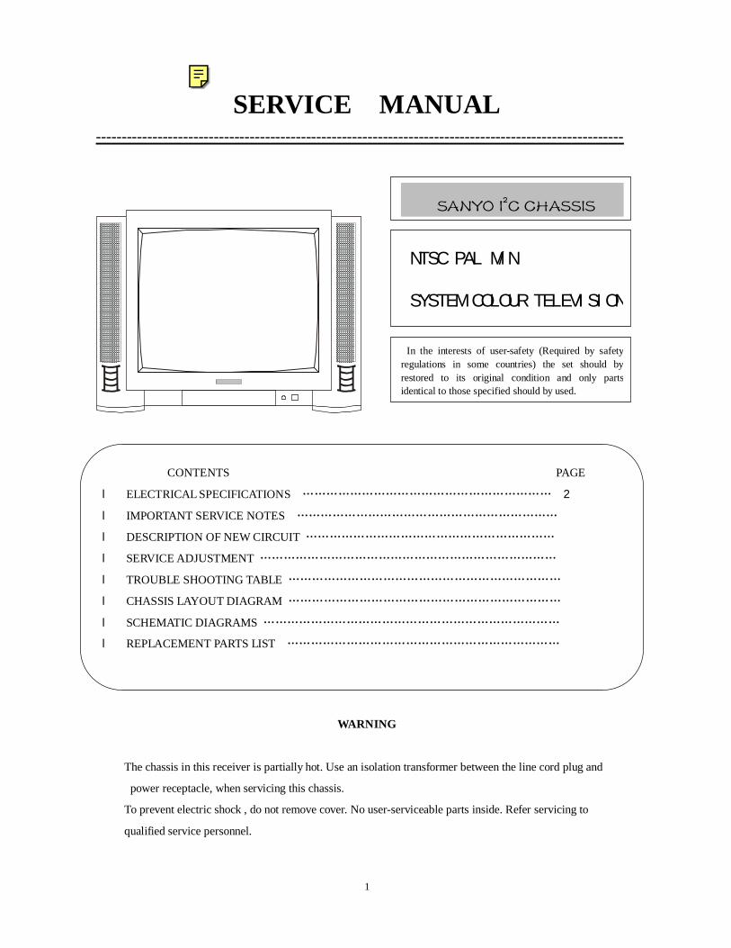
SERVICE MANUAL -------------------------------------------------------------------------------------------------------
WARNING
The chassis in this receiver is partially hot. Use an isolation transformer between the line cord plug and
power receptacle, when servicing this chassis.
To prevent electric shock , do not remove cover. No user-serviceable parts inside. Refer servicing to
qualified service personnel.
In the interests of user-safety (Required by safety regulations in some countries) the set should by restored to its original condition and only parts identical to those specified should by used.
CONTENTS PAGE
l ELECTRICAL SPECIFICATIONS ……………………………………………………… 2
l IMPORTANT SERVICE NOTES …………………………………………………………
l DESCRIPTION OF NEW CIRCUIT ………………………………………………………
l SERVICE ADJUSTMENT …………………………………………………………………
l TROUBLE SHOOTING TABLE ……………………………………………………………
l CHASSIS LAYOUT DIAGRAM ……………………………………………………………
l SCHEMATIC DIAGRAMS …………………………………………………………………
l REPLACEMENT PARTS LIST ……………………………………………………………
SANYO I2C CHASSIS
NTSC PAL M/N
SYSTEM COLOUR TELEVISION
2
ELECTRICAL SPECIFICATIONS Aerial Input Impedance…………………………………………………………………… 750hm unbalanced Convergence…………………………………………………………………………… self-converging system Focus……………………………………………………………………… Electrostatic focus high bi-potential Audio Power Output Rating………………………………………………………………………… 3WX2 at max Picture IF.Freq.………………………………………………………………………… 45.75MHz Sound carrier Trap………………………………………………………………………… 41.25MHz Power Source…………………………………………………………………………… 110/220V AC 60HZ/50HZ Power Consumption……………………………………………………………………… 120W Speaker Size………………………………………………………………………… Round DynamicX2pcs. Sweep Deflection………………………………………………………………………………… Magnetic Tuning Ranges………………………………………………………………………… VHF-Channels 2-13
UHF-Channels 14-83
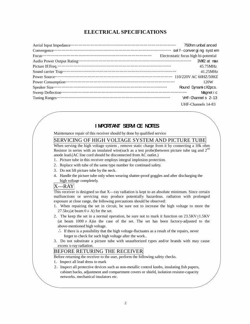
IMPORTANT SERVICE NOTES
Maintenance repair of this receiver should by done by qualified service
SERVICING OF HIGH VOLTAGE SYSTEM AND PICTURE TUBE When serving the high voltage system , remove static charge from it by connecting a 10k ohm Resistor in series with an insulated wire(such as a test probe)between picture tube tag and 2nd
anode lead.(AC line cord should be disconnected from AC outlet.) 1.Picture tube in this receiver employs integral implosion protection. 2.Replace with tube of the same type number for continued safety. 3.Do not lift picture tube by the neck. 4.Handle the picture tube only when wearing shatter-proof goggles and after discharging the high voltage completely. X---RAY This receiver is designed so that X---ray radiation is kept to an absolute minimum. Since certain malfunctions or servicing may produce potentially hazardous. radiation with prolonged exposure at close range, the following precautions should be observed: 1. When repairing the set in circuit, be sure not to increase the high voltage to more the
27.5kv,(at beam 0μA) for the set. 2. The keep the set in a normal operation, be sure not to mark it function on 23.5KV+1.5KV
(at beam 1000μA)in the case of the set. The set has been factory-adjusted to the above-mentioned high voltage.
∴ If there is a possibility that the high voltage-fluctuates as a result of the repairs, never forget to check for such high voltage after the work.. 3. Do not substitute a picture tube with unauthorized types and/or brands with may cause
excess x-ray radiation. BEFORE RETURING THE RECEIVER Before returning the receiver to the user, perform the following safety checks. 1.Inspect all lead dress to mark
2.Inspect all protective devices such as non-metallic control knobs, insulating fish papers, cabinet backs, adjustment and compartment covers or shield, isolation resistor-capacity networks, mechanical insulators etc.
3
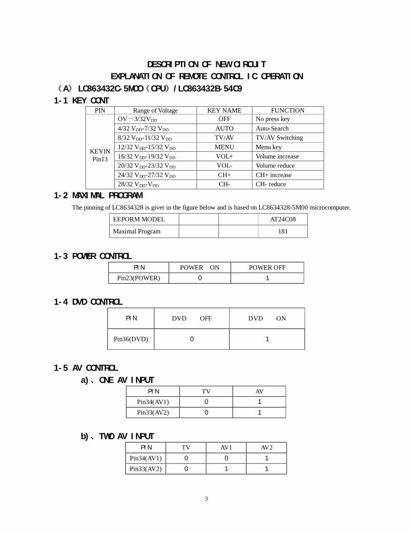
DESCRIPTION OF NEW CIRCUIT
EXPLANATION OF REMOTE CONTROL IC OPERATION
(A) LC863432C-5MOO(CPU)/LC863432B-54C9
1-1 KEY CONT PIN Range of Voltage KEY NAME FUNCTION
OV~3/32VDD OFF No press key 4/32 VDD-7/32 VDD AUTO Auto-Search 8/32 VDD-11/32 VDD TV/AV TV/AV Switching 12/32 VDD-15/32 VDD MENU Menu key 16/32 VDD-19/32 VDD VOL+ Volume increase 20/32 VDD-23/32 VDD VOL- Volume reduce 24/32 VDD-27/32 VDD CH+ CH+ increase
KEYIN Pin13
28/32 VDD-VDD CH- CH- reduce
1-2 MAXIMAL PROGRAM
The pinning of LC8634328 is giver in the figure below and is based on LC8634328-5M00 microcomputer.
EEPORM MODEL AT24C08
Maximal Program 181
1-3 POWER CONTROL
PIN POWER ON POWER OFF Pin23(POWER) 0 1
1-4 DVD CONTROL
PIN DVD OFF DVD ON
Pin36(DVD) 0 1
1-5 AV CONTROL
a)、ONE AV INPUT PIN TV AV
Pin34(AV1) 0 1
Pin33(AV2) 0 1
b)、TWO AV INPUT
PIN TV AV1 AV2 Pin34(AV1) 0 0 1
Pin33(AV2) 0 1 1

4
c)、THREE AV INPUT PIN TV AV1 AV2 AV3
Pin34(AV1) 0 1 0 1
Pin33(AV2) 0 0 1 1
1-6 50/60 CONTROL OUTPUT PIN 50 60
Pin35(50/60) 0 1
1-7 LC863432C Pin Connection(top view)
WOOF
YUV
SDA1 DVD ON/OFF
DEGAUSS
VOLUME-
1 36
CLK1
SDA0
CLK0
VDD
VSSXT1
XT2
KEY-IN
AFT-IN
NC
X-RAY
RESET
FILT
CVIN
BALNK2
V-SYNC
H-SYNC
2
3 4 5
6
7
8
9
10
11
12
13
14
15
16
17
18
DVD
AV1
AV2
VOLUME-
REMOT
SD
ENABL
MUTE POWER
BLANK
BLUE
GREEN
RED
35
34
33
32
31
3029
28
27
26
25
2423
22
21
2019
5
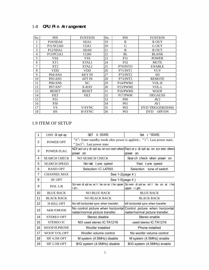
1-8 CPU Pin Arrangement
No. PIN FUNTION No. PIN FUNTION 1 P10/SDA0 SDA1 19 R R OUT 2 P11/SCLK0 CLK1 20 G G OUT 3 P12/SDA1 SDA0 21 B B OUT 4 P13/PCLK1 CLK0 22 BL BLANK 5 VSS VSS 23 P31 POWER 6 XT1 XTAL1 24 P32 MUTE 7 XT2 XTAL2 25 P70/INTO ENABLE 8 VDD VDD 26 P71/INT1 YUV 9 P04/AN4 KEY IN 27 P72/INT2 SD
10 P05/AN5 AFT IN 28 P73/INT3 REMOTE 11 P06/AN6 NC 29 P14/PWM1 VOL-R 12 P07/AN7 X-RAY 30 P15/PWM2 VOL-L 13 RESET RESET 31 P16/PWM3 WOOF 14 FILT FILT 32 P17/PWM DEGAUSS 15 P33 33 P00 AV2 16 P30 34 P01 AV1 17 VS V-SYNC 35 P02 DVD TRIGGER(50/60) 18 HS H-SYNC 36 P03 DVD OFF/ON
1.9 ITEM OF SETUP
1 OSD Display SET 0 STATE Set 1 ”STATE
2 POWER OPT “0”:Enter standby mode after power is applied.;“1”:Last power state;“2or3”:Last power state.
3 POWER FLAG NO factory display on screen when
power on
Factory display on screen when
power on
4 SEARCH CHECK NO SEARCH CHECK Search check when power on
5 SEARCH SPEED Normal tune speed Fast tune speed
6 BAND OPT Selection IC LA7910 Selection tune of switch 7 CHANNEL MAX See 1-2(page 4 ) 8 AV OPT See 1-5(page 4 )
9 POS. L/R Screen display will be on at the upper
left.
Screen display will be on at the
upper right.
10 BLUE BACK NO BLUE BACK BLUE BACK 11 BLACK BACK NO BLACK BACK BLACK BACK 12 H-KILL OPT No kill horizontal sync when transfer. kill horizontal sync when transfer.
13 AKB P.MODE No control picture when horizontal raster/normal picture transfer.
Control picture when horizontal raster/normal picture transfer.
14 STEREO OPT Stereo disable Stereo enable 15 STEREO IC NO used stereo IC:TA1216 used stereo IC:TA1216 16 WOOF/H.PHONE Woofer installed Phone installed 17 WOOF VOL.OPT Woofer volume control No woofer volume control 18 SIF 4.5M OPT M system (4.5MHz) disable M system (4.5MHz) enable 19 SIF 5.5M OPT B/G system (4.5MHz) disable B/G system (4.5MHz) enable
6
20 SIF 6.0M OPT I system (4.5MHz) disable I system (4.5MHz) enable 21 SIF 6.5M OPT D/K system (4.5MHz) disable D/K system (4.5MHz) enable 22 SIF AUTO OPT No auto sound system detecting Auto sound system detecting 23 PAL OPT PAL system disable PAL system enable 24 N3.58 OPT N3.58 system disable N3.58 system enable 25 N4.43 OPT N4.43 system disable N4.43 system enable 26 SECAM OPT SECAM system disable SECAM system enable 27 COL-AUTO OPT NO auto color system detecting Auto color system detecting 28 IC TEST NORMAL“0”
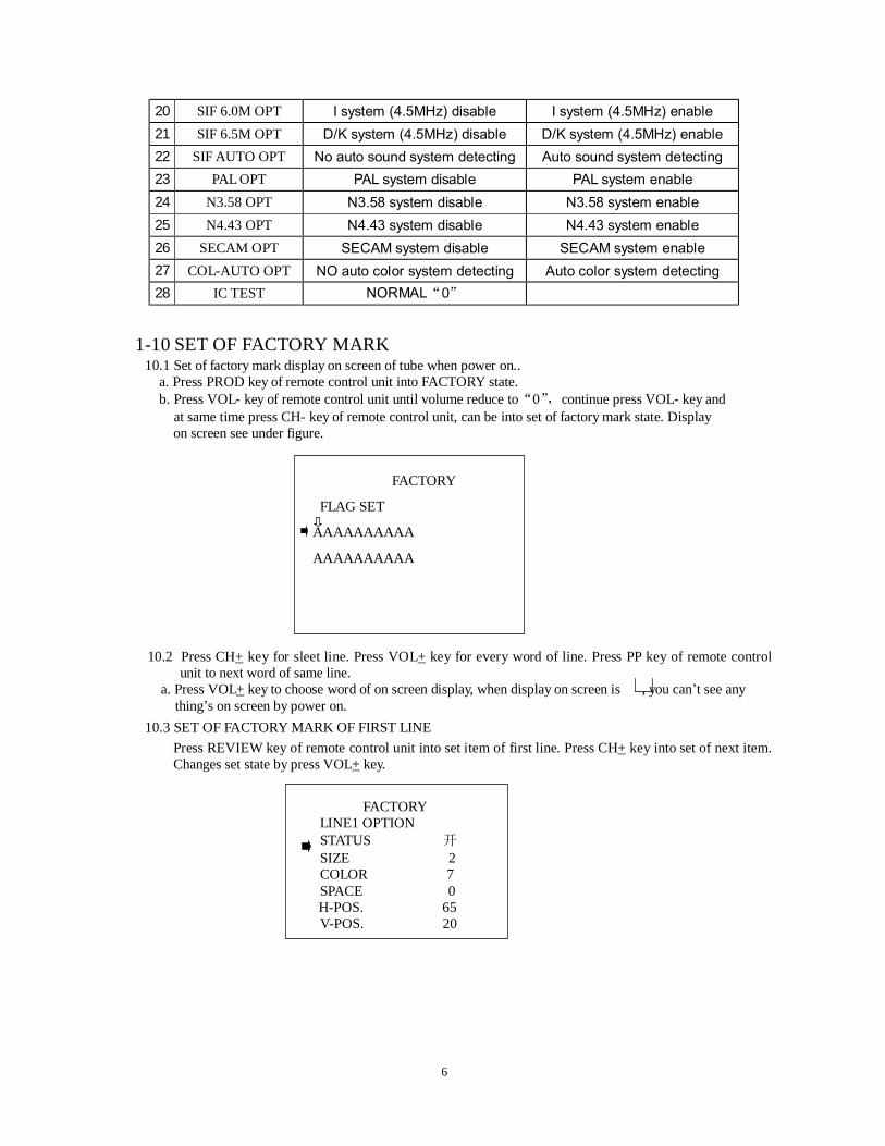
1-10 SET OF FACTORY MARK
10.1 Set of factory mark display on screen of tube when power on.. a. Press PROD key of remote control unit into FACTORY state.
b. Press VOL- key of remote control unit until volume reduce to“0”,continue press VOL- key and at same time press CH- key of remote control unit, can be into set of factory mark state. Display
on screen see under figure. FACTORY
FLAG SET
AAAAAAAAAA
AAAAAAAAAA
10.2 Press CH+ key for sleet line. Press VOL+ key for every word of line. Press PP key of remote control
unit to next word of same line. a. Press VOL+ key to choose word of on screen display, when display on screen is , you can’t see any
thing’s on screen by power on. 10.3 SET OF FACTORY MARK OF FIRST LINE
Press REVIEW key of remote control unit into set item of first line. Press CH+ key into set of next item. Changes set state by press VOL+ key.
FACTORY LINE1 OPTION STATUS 开 SIZE 2 COLOR 7 SPACE 0 H-POS. 65 V-POS. 20
7
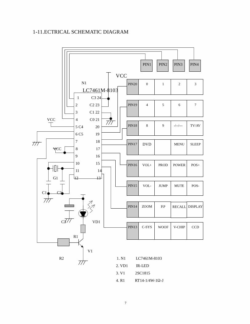
1-11.ECTRICAL SCHEMATIC DIAGRAM VCC N1
LC7461M-8103 1 C3 24
2 C2 23
3 C1 22
VCC 4 C0 21
5 C4 20
6 C5 19
7 18
VCC 8 17
9 16
10 15
11 14
G1 12 13
C1 C2
C3 VD1
R1
V1
R2 1. N1 LC7461M-8103
2. VD1 IR-LED
3. V1 2SC1815
4. R1 RT14-1/4W-1Ω-J
PIN1 PIN4 PIN2 PIN3
3 1 2 0 PIN20
7 5 6 4 PIN19
TV/AV 9 -/--/--- 8 PIN18
SLEEP
MENU
DVD
PIN17
POS+
PROD
POWER
VOL+
PIN16
POS-
JUMP
MUTE
VOL-
PIN15
DISPLAY
P.P
RECALL
ZOOM PIN14
CCD
WOOF
V-CHIP
C-SYS PIN13
8
User code: 5. R2 RT14-1/4W-220Ω-J
C5 C4 C3 C2 C1 C0 6. C1 C2 CT1-05B-2B4-63V-220PF-K
0 1 1 1 0 0 7. C3 CD110X-6.3V-100UF-M
8. G1 455KHZ 9.VCC 2 pcs. AA batteries
Infrared remote control unit for service code:
C5 C4 C3 C2 C1 C0
1 1 1 1 0 1
Infrared remote control unit for use code:
C5 C4 C3 C2 C1 C0
0 1 1 1 0 0
Infrared remote control unit for users:
Pin1 Pin2 Pin3 Pin4
Pin20 0 1 2 3
19 4 5 6 7
18 8 9 -- TV/AV
17 NICAM AUDIO WOOF
16 VOL+ PROD MUTE CH+
15 VOL- CHANNEL POWER CH-
14 PICTURE PP REVIEW CALL
13 SLEEP CLOCK PRESET SYSTEM
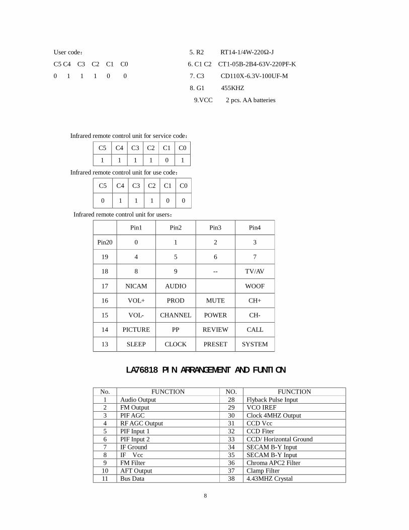
LA76818 PIN ARRANGEMENT AND FUNTION
No. FUNCTION NO. FUNCTION 1 Audio Output 28 Flyback Pulse Input 2 FM Output 29 VCO IREF 3 PIF AGC 30 Clock 4MHZ Output 4 RF AGC Output 31 CCD Vcc 5 PIF Input 1 32 CCD Fiter 6 PIF Input 2 33 CCD/ Horizontal Ground 7 IF Ground 34 SECAM B-Y Input 8 IF Vcc 35 SECAM B-Y Input 9 FM Filter 36 Chroma APC2 Filter
10 AFT Output 37 Clamp Filter 11 Bus Data 38 4.43MHZ Crystal
9
12 Bus Clock 39 Chroma APC1 Filter 13 ABL 40 Selected Video Output 14 Red Input 41 Video /Vertical /Bus Ground 15 Greed Input 42 External Video Input(Y-IN) 16 Blue Input 43 Video/Vertical Vcc 17 Fast Blanking Input 44 Internal Video Input(C-IN) 18 RGB Vcc 45 Black Lever Detector 19 Red Output 46 Video Output 20 Green Output 47 VCO Filter 21 Blue Output 48 VCO Coil 2 22 Fsc output or c_sync output 49 VCO Coil 1 23 Vertical Output 50 APC Filter 24 RAMP ALC Filter 51 Ext.Audio Input 25 Horizontal /Bus Vcc 52 SIF Output 26 Horizontal AFC Filter 53 SIF APC Filter 27 Horizontal Output 54 SIF Input
SERVICE ADJUSTMENT
1. Adjustment +B Voltage RP551 1.1 Test point--------- Two point of C561
1.2 Adjust RP551 so that the voltage (DC) becomes: 14 110V(CHAI HONG Tube) 21’’ 110V(CHAI HONG Tube) 25’’ 125V/130V(CHAI HONG Tube/HUA FEI Tube) 29’’ 125V(CHAI HONG Tube)
2. Adjustment of AFT: T101 2.1 Connect signal generator to the test point C101 CW…..38MHz/38.9MHz 80db 2.2 Connect digital voltmeter on point of R113 and R114. 2.3 Adjust T101(PIF detector coil) so that the detection output voltage(DC) becomes 3.6+0.02V。 3. Adjustment of RF-AGC 3.1 Receive Philips pattern signal. 3.2 Sweep output ......62+1db 3.3 Connect digital voltmeter on point TP-A. 3.4 Press PROD key of remote control unit into ADTUST state. 3.5 Press CH+ key until adjustment item becomes RF—AGC. Press VOL+ key of remote control unit so that voltage of digital voltmeter display becomes 5.5+0.1V 3.6 Press PROD key of remote control unit until normal.
4. Adjustment of Vertical size 4.1 Receive Philips pattern signal(PAL system). 4.2 Press PROD key of remote control unit into ADTUST state. 4.3 Press CH+ key until adjustment item becomes V.SIZE. Press VOL+ key of remote control unit so that vertical over scan is at 8%. 4.4 Receive Philips pattern signal(NTSC system) in AV state. 4.5 Press CH+ key until adjustment item becomes NT.V.SIZE. Press VOL+ key of remote control unit so that vertical over scan is at 8%.
10
4.6 Press PROD key of remote control unit until normal.
5. Adjustment of Vertical center 5.1 Receive Philips pattern signal (PAL system). 5.2 Press PROD key of remote control unit into ADTUST state.
5.3 Press CH+ key until adjustment item becomes V.POSI . Press VOL+ key of remote control unit so that vertical center of picture comes mostly close to the geometrical center of CRT.
5.4 Receive Philips pattern signal (NTSC system) in AV state. 5.5 Press CH+ key until adjustment item becomes NT.V.POSI.. Press VOL+ key of remote control unit so that vertical center of picture comes mostly close to the geometrical center of CRT.
5.6 Press PROD key of remote control unit until normal.
6. Adjustment of Vertical line 6.1 Receive Philips pattern signal (PAL system). 6.2 Press PROD key of remote control unit into ADTUST state.
6.3 Press CH+ key until adjustment item becomes V.LINE . Press VOL+ key of remote control unit so that vertical line of picture comes mostly close normal.
6.4 Receive Philips pattern signal (NTSC system) in AV state. 6.5 Press CH+ key until adjustment item becomes NT.V.LINE . Press VOL+ key of remote control unit so that vertical line of picture comes mostly close normal.
6.6 Press PROD key of remote control unit until normal.
7. Adjustment of Sign horizontal/vertical positioning 7.1 Receive Philips pattern signal (PAL system). 7.2 Press PROD key of remote control unit into ADTUST state.
7.3 Press CH+ key until adjustment item becomes OSD.H.POSI. Press VOL+ key of remote control unit so that title sign of on screen ADJUST at horizontal center of Philips pattern signal. 7.4 Press CH+ key until adjustment item becomes OSD.V.POSI. Used VOL+ key of remote control unit
so that sign of on screen ADJUST in title block of Philips pattern signal. 7.5 Press CH+ key until adjustment item becomes OSD.CONT. . Press VOL+ key of remote control unit
so that OSD contrast can be seed clear. 7.6 Press PROD key of remote control unit until normal. 8. Adjustment of background
8.1 Receive white pattern signal. 8.2 Press PROD key of remote control unit into B/W adjustment state.
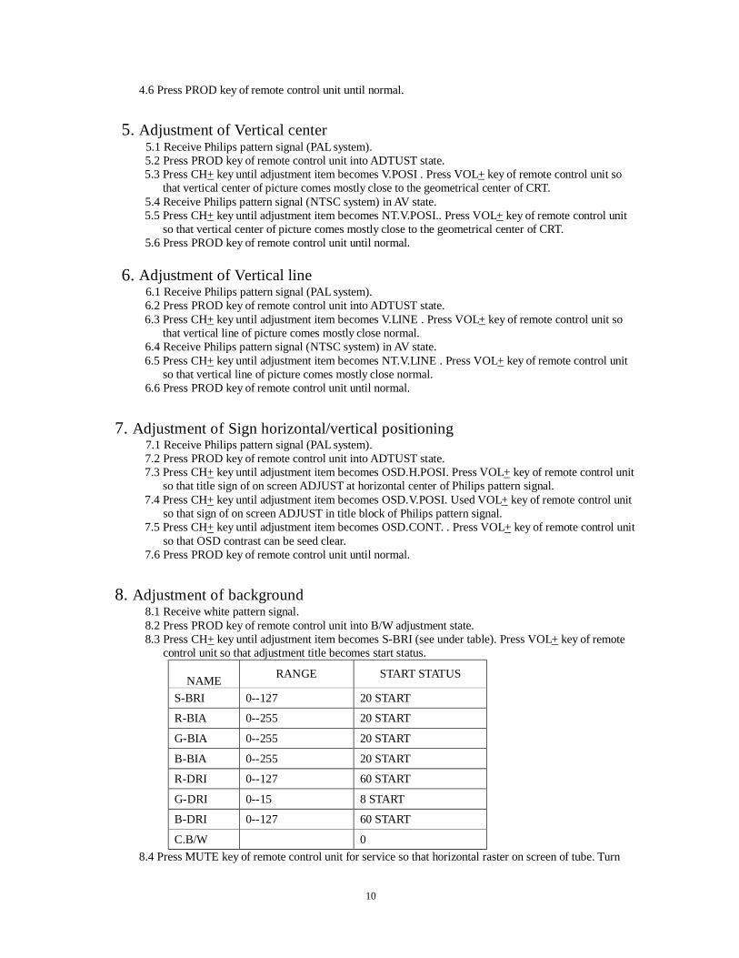
8.3 Press CH+ key until adjustment item becomes S-BRI (see under table). Press VOL+ key of remote control unit so that adjustment title becomes start status.
NAME RANGE START STATUS
S-BRI 0--127 20 START
R-BIA 0--255 20 START
G-BIA 0--255 20 START
B-BIA 0--255 20 START
R-DRI 0--127 60 START
G-DRI 0--15 8 START
B-DRI 0--127 60 START
C.B/W 0 8.4 Press MUTE key of remote control unit for service so that horizontal raster on screen of tube. Turn
11
SCREEN of FBT. Counter clockwise until horizontal raster of either of three colors R.G. and B Appears slightly on CRT. Here, one of the three colors appears as screen control is turned. 8.5 Adjust bias controls (two of R-BIA, G-BIA, B-BIA) other than that belonging to displayed color to make white the horizontal raster.(under white the horizontal raster state, “2”and“3”//“4”and “5”//“6”and“7”key of remote control unit can be in crease and in reduce for R-BIA G-BIA B- BIA . 8.6 Press NUTE key on infrared remote control unit to picture normal state. Press CH+ key until adjustment item becomes C.B/W, press VOL+ key of remote control unit until becomes 2. Press CH+ key until adjustment item becomes S-BRT, press VOL+ key of remote control unit until becomes 99. Adjustment R.DRI/ G.DRI/. B.DRI until picture becomes white by press CH+, VOL+ key. 8.7 Press PROD key of remote control unit until normal.
10. ADJUST ITEM/SETUP ITEM TABLE
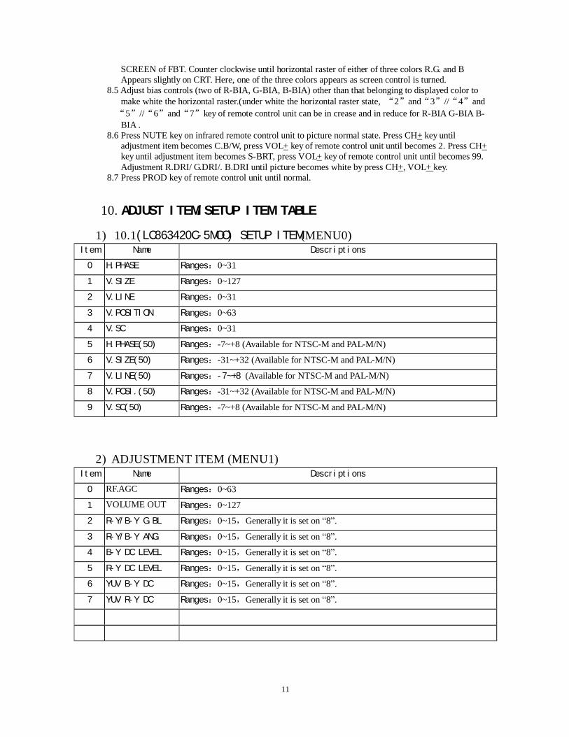
1) 10.1(LC863420C-5MOO) SETUP ITEM(MENU0) Item Name Descriptions
0 H.PHASE
Ranges:0~31
1 V.SIZE Ranges:0~127
2 V.LINE Ranges:0~31
3 V.POSITION Ranges:0~63
4 V.SC Ranges:0~31
5 H.PHASE(50) Ranges:-7~+8 (Available for NTSC-M and PAL-M/N)
6 V.SIZE(50) Ranges:-31~+32 (Available for NTSC-M and PAL-M/N)
7 V.LINE(50) Ranges:-7~+8 (Available for NTSC-M and PAL-M/N)
8 V.POSI.(50)
Ranges:-31~+32 (Available for NTSC-M and PAL-M/N)
9 V.SC(50) Ranges:-7~+8 (Available for NTSC-M and PAL-M/N)
2) ADJUSTMENT ITEM (MENU1)
Item Name Descriptions
0 RF.AGC Ranges:0~63
1 VOLUME OUT Ranges:0~127
2 R-Y/B-Y G.BL Ranges:0~15,Generally it is set on “8”.
3 R-Y/B-Y ANG. Ranges:0~15,Generally it is set on “8”.
4 B-Y DC LEVEL Ranges:0~15,Generally it is set on “8”.
5 R-Y DC LEVEL Ranges:0~15,Generally it is set on “8”.
6 YUV B-Y DC Ranges:0~15,Generally it is set on “8”.
7 YUV R-Y DC Ranges:0~15,Generally it is set on “8”.
12
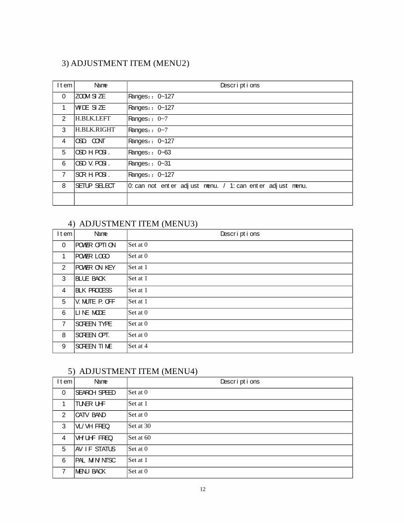
3) ADJUSTMENT ITEM (MENU2)
Item Name Descriptions
0 ZOOM SIZE Ranges::0~127
1 WIDE SIZE Ranges::0~127
2 H.BLK.LEFT Ranges::0~7
3 H.BLK.RIGHT Ranges::0~7
4 OSD. CONT Ranges::0~127
5 OSD H.POSI. Ranges::0~63
6 OSD V.POSI. Ranges::0~31
7 SCR.H.POSI. Ranges::0~127
8 SETUP SELECT 0:can not enter adjust menu. / 1:can enter adjust menu.
4) ADJUSTMENT ITEM (MENU3)
Item Name Descriptions
0 POWER OPTION Set at 0
1 POWER LOGO Set at 0
2 POWER ON KEY Set at 1
3 BLUE BACK Set at 1
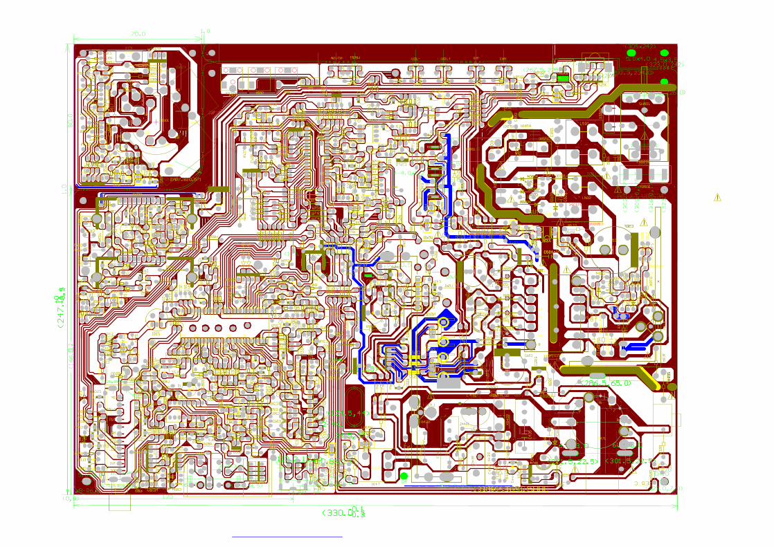
4 BLK PROCESS Set at 1
5 V.MUTE P.OFF Set at 1
6 LINE MODE Set at 0
7 SCREEN TYPE Set at 0 8 SCREEN OPT. Set at 0 9 SCREEN TIME Set at 4
5) ADJUSTMENT ITEM (MENU4) Item Name Descriptions
0 SEARCH SPEED Set at 0
1 TUNER UHF Set at 1
2 CATV BAND Set at 0
3 VL/VH FREQ. Set at 30
4 VH/UHF FREQ. Set at 60
5 AV IF STATUS Set at 0
6 PAL M/N/NTSC Set at 1
7 MENU BACK Set at 0

13
8 PROMPT TYPE Set at 1
9 X-RYA LEVEL Set at 43
6) ADJUSTMENT ITEM (MENU5) Item Name Descriptions
0 AV OPTION Set at 2
1 S-VIDEO OPT. Set at 1
2 YUV OPTION Set at 0
3 ONLY AV MODE Set at 0
4 DVD OPTION Set at 1
5 DVD OFF TIME Set at 6
6 OFF TRIGGER Set at 120
7 ON TRIGGER Set at 120
8 DVD KEY DEF. Set at 0
9 DVD PORT DEF Set at 1
7) ADJUSTMENT ITEM (MENU6)
Item Name Descriptions
0 CALENDAR Set at 1
1 ZOOM OPTION Set at 1
2 CHILD LOCK Set at 1
3 REMEMBER AV Set at 1
4 CCD OPTION Set at 1
5 VCHIP OPTION Set at 1
6 V-PASSWORD Set at 1
7 HOTEL MODE Set at 0
8 HOTEL VOLUME Set at 10
9 ON POSITION Set at 137
8) ADJUSTMENT ITEM (MENU7)
Item Name Descriptions
0 ENGLISH OSD Set at 1
1 FRANCE OSD Set at 1
2 SPANISH OSD Set at 1
3 PORTUGUESE Set at 1
4 CHINESE OSD Set at 0
14
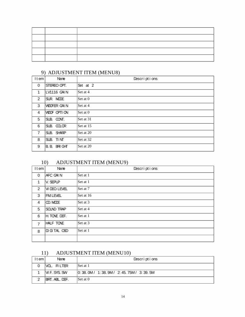
9) ADJUSTMENT ITEM (MENU8)
Item Name Descriptions
0 STEREO OPT. Set at 2
1 LV1116 GAIN Set at 4
2 SUR. MODE Set at 0
3 WOOFER GAIN Set at 4
4 WOOF OPTION Set at 0
5 SUB. CONT. Set at 31
6 SUB. COLOR Set at 15
7 SUB. SHARP Set at 20
8 SUB. TINT Set at 32
9 B.B. BRIGHT Set at 20
10) ADJUSTMENT ITEM (MENU9)
Item Name Descriptions
0 AFC GAIN Set at 1
1 V.SEPUP Set at 1
2 VIDEO.LEVEL Set at 7
3 FM.LEVEL Set at 16
4 CD.MODE Set at 3
5 SOUND TRAP Set at 4
6 H.TONE DEF. Set at 1
7 HALF TONE Set at 3
8 DIGITAL OSD Set at 1
11) ADJUSTMENT ITEM (MENU10)
Item Name Descriptions
0 VOL. FILTER Set at 1
1 VIF.SYS.SW 0:38.0M / 1:38.9M / 2:45.75M / 3:39.5M
2 BRT.ABL.DEF. Set at 0
15
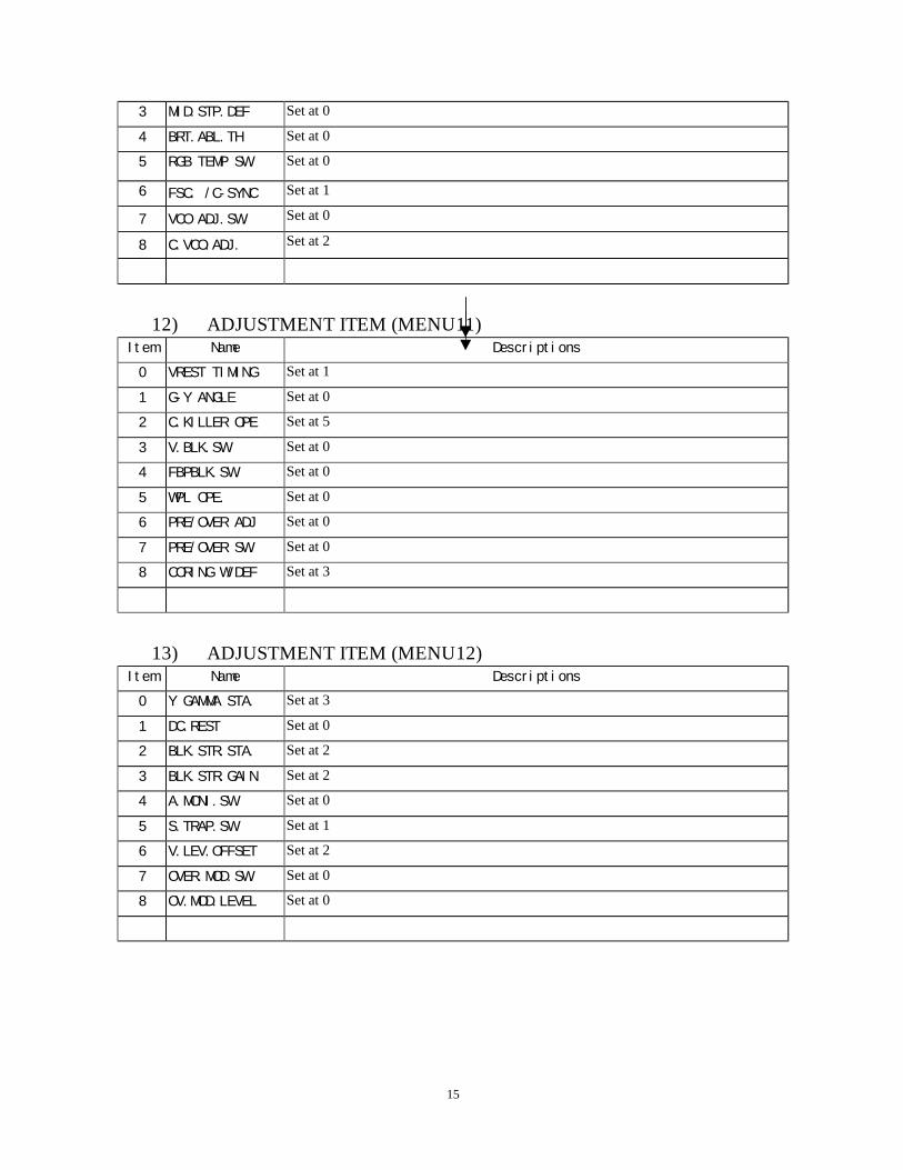
3 MID.STP.DEF Set at 0
4 BRT.ABL.TH Set at 0
5 RGB TEMP SW. Set at 0
6 FSC. /C-SYNC Set at 1
7 VCO ADJ.SW. Set at 0
8 C.VCO.ADJ. Set at 2
12) ADJUSTMENT ITEM (MENU11)
Item Name Descriptions
0 VREST TIMING Set at 1
1 G-Y ANGLE Set at 0
2 C.KILLER OPE Set at 5
3 V.BLK.SW Set at 0
4 FBPBLK.SW. Set at 0
5 WPL OPE. Set at 0
6 PRE/OVER ADJ Set at 0
7 PRE/OVER SW. Set at 0
8 CORING W/DEF Set at 3
13) ADJUSTMENT ITEM (MENU12)
Item Name Descriptions
0 Y GAMMA STA. Set at 3
1 DC.REST Set at 0
2 BLK.STR.STA. Set at 2
3 BLK.STR.GAIN Set at 2
4 A.MONI.SW Set at 0
5 S.TRAP.SW Set at 1
6 V.LEV.OFFSET Set at 2
7 OVER.MOD.SW. Set at 0
8 OV.MOD.LEVEL Set at 0
16
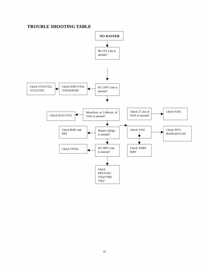
TROUBLE SHOOTING TABLE
NO RASTER
B6 12V Line is normal?
B1 110V Line isnormal?
Check N501/V554 /VD554/R569
Check D551/V551
Check V513/V512 /V511/V501
Waveform at Collector of V431 is normal?
Heater voltage is normal?
B3 190V Line is normal?
Check R491 and FBT
Check VD552
Check FBT/V431/ V432/V902 V922
Check 27 pin of N101 is normal?
Check N101
Check V432 Check T471/ R439L441/C441
Check XS901 R491
17
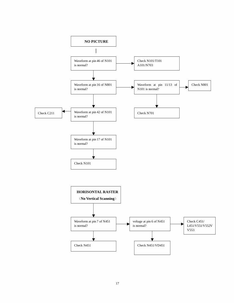
|
NO PICTURE
Waveform at pin 46 of N101 is normal?
Waveform at pin 16 of N801 is normal?
Waveform at pin 42 of N101 is normal?
Waveform at pin 17 of N101 is normal?
Check N101
HORISONTAL RASTER
(No Vertical Scanning)
Waveform at pin 7 of N451 is normal?
Check N451
Check N101/T101 A101/N703
Waveform at pin 11/13 of N101 is normal?
Check N801
Check C211 Check N701
voltage at pin 6 of N451 is normal?
Check C451/ L451/V551/V552VV553
Check N451/VD451
18
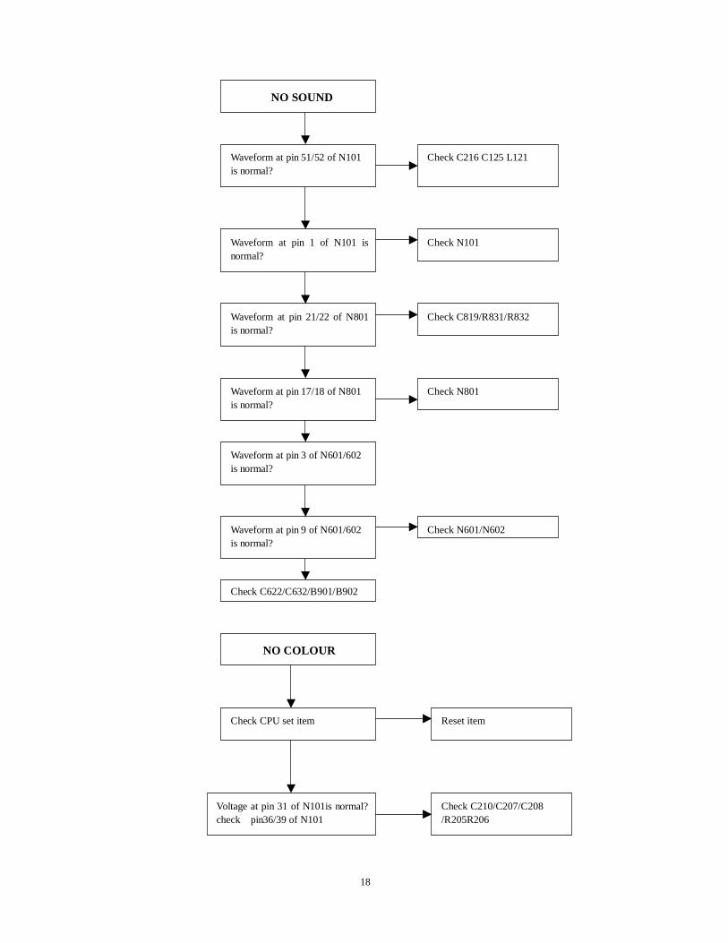
NO SOUND
Waveform at pin 51/52 of N101 is normal?
Waveform at pin 1 of N101 is normal?
Waveform at pin 21/22 of N801is normal?
Waveform at pin 17/18 of N801 is normal?
Waveform at pin 3 of N601/602 is normal?
Waveform at pin 9 of N601/602 is normal?
Check C622/C632/B901/B902
Check C216 C125 L121
Check N101
Check C819/R831/R832
Check N801
Check N601/N602
NO COLOUR
Check CPU set item
Voltage at pin 31 of N101is normal? check pin36/39 of N101
Reset item
Check C210/C207/C208 /R205R206
K6D
LIVE AREA
B1-ADJ
NOTE:
(3) D: 1S1555; 1N4148; 1S2473; 1S2076; D5442;
AC220V50HZ
(4) 0.01:CT1-08B-2F4-63V-0.01uF-Z;
(5) KK470: CT1-06B-2B4-63V-470uF-K
(6) FKXXX: CL11-63V-XXXuF-K
(7) 200NJXXX: CBB22-200V-XXXuF-J
(8) 1500MJXXX: CBB12-1600V-XXXuF-J
HV
FO
SCREEN
ABL
H-PULSE
(1) 2SC: 2SC536-E/F/G; 2SC1815-O/Y/GR;
(2) 2SA: 2SA608-E/F; 2SA1015-O/Y/GR;
FO
5
4
3
2
1
9
1 2
34
28
CRT BOARD
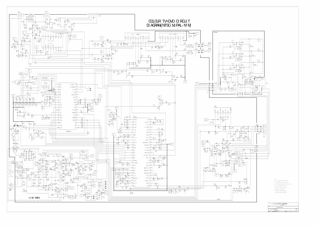
COLOUR TV+DVD CIRCUITDIAGRAM(NTSC-M,PAL-N/M)
Lout
Vout
Rout
V1in
L1in
R1in
13
14
16
15
11
12
10
6
Y C
ET-5A5E-AF108AT
TH818.SCH 1
PALM PALN NTSC
TV + DVD (LA76818+LC863448)TH818.SCH
1 1Friday, March 25, 2005
Title
Size Document Number Rev
Date: Sheet of
1
611
8
2
10
1
1
2
1
1
7 1
7
9
2
2
2
10
4
5
3
4
3
3
4
3
9
4
C5162KV470
C5512KV470
C554
1KV470
C515FJ0.015
C501250HM0.22
C513FK4700
L909LJ0107CHA
C5031000KM1000E
C5051000KM1000E
C5041000KM1000E
C5061000KM1000E
C532400KM470S
C533400KM2200S
V5542SB892
V5532SC
V5112SA
V5122SC3807
VD554FR104
RP551B-2K
VD592RGP30B
VD5031N5408 VD505
1N5408
VD5061N5408
C56525V100
+
C507400V220
+C561160V470
+
VD517ES1
VD5041N5408
R5252SJ68
L504Z2073
DVD5V
B69V
V5132SC4460
C514FK0.1
VD551RU3C
VD518D
VD514D
VD516D
R5115.6K
R5231.8K
R5171K
R515DJ22K
R51922
R5535.6K
R554150K
R5551/2DJ47K
R55622K
R56610K
R5512SJ22K
R52215K
R5321/2CK5.6M
R5311/2CK5.6M
R5601/2SJ10K
C59216V1000
+
C517FJ0.015
N501PC817B
L501LG-003
L502LG-003
R5262.2K
R5201/2SJ120K
R5211/2SJ68K
VD519HZ7C1
VD555RGP10G
C59516V1000
+
N551AN7809
123
R5521/2DJ100K
C5181000KK1000E
FU501T2.5A250V
00 0
U902EW0130KB
R5025WK1.8
XS501
TJC2-2A
RT501MZ73-18
000
R5691FJ2.2
R5622FJ1
L433Z2073
KQ
XS402TJC2-5A
XP402TJC2-5Y
V432TT2190/2SD2499
B1110V
R4911FJ1.5
C4381500MJ9100
B424V
R4342W/270
R4411/2SJ1K
C444160V4.7
+
R446220K
R41310K
C437100VNJ0.47
R41210K
C21150V1
+
W902 JG0034
R93582
V9322SC
C93116V10
+ C93450V0.47
+
R902100
R912100
R922100
R924330
C921CJ390
C911
CJ390
C901CJ390
XS901GZS10-2-102G
C9392KV1000
R9181/2SJ2.7K
R9281/2SJ2.7K
R904330
C903CJ56R
R914330
C913CJ56R
C923CJ56R
R9311K
U901XXXXXXX
R9081/2SJ2.7K
R900DJ10K
V9022SC2688
V9122SC2688
V9222SC2688
C93216V10
+
R906820
R916820
R93215K
R9331.5K
R9072SJ10K
R9172SJ10K
R9272SJ10K
R926820
R94033
K9NTJC2-2A
KQ
KP
C93316V1000
+
B217V
B75V
B69V
B75V
B69V
B69V
DVD5V
B1110V
B75V
B69V
B217V
B55V
B3190V
B69V
R5242SJ27
C1100.01
R1084.7K
R1091.2K
R110220
R10733
V1022SC2216 C112
0.01
R11133
C1110.01
L10222UH
C11516V100
+ C1160.01
C11750V1
+R113100K
R114100K
C1180.01
C1190.01
C120FK0.022
C121FK0.047
C1220.01
C1231000
R1211K
C12518
T101ST6019
R2011K
R2021K
R204390K
C20350V2.2
+
C20450V1
+
C2050.01
C20616V47
+
C207FK0.1
C20850V0.47
+
R20610K
C20818P
G201S4.43
R20510K
C27616V10
+
C27816V47
+C2770.01
R273J4.7K
R4082.2K
R432J
R4331/2SJ1K
C433500KK3900
T431YFTX40
B424V
R4538.2K
R4542.7K
R45512K
R45612K
R45739K
C45625V2.2
+
R4581K
C45725V2200
+
R4601/2DJ180 C458
100FK0.033
R461A1/2DJ120
R4591SJ1
C40150V0.47
+R4012.2K
C40416V100
+ C4050.01
C406FK0.033
C40750V1
+
R4023.3K
R40647K
R4042.7K
C40850V1
+
R241100
R242100
R24333
C24416V47
+ C2450.01
C6370.01
C63225V2200
+
XS602TJC3-2A
XP602TJC3-2Y
B9028W8OHM
B9018W8OHM
KP
L4410449
R5632SJ27
R56110K
R5671.2K
L431YC0008
C403FK0.47
C402FK0.22
R1191K
C57210V470
+
C45016V100
+
R409680
C431X
C210
16V10+
C13750V0.47
+
C13950V0.47
+
R127220
Z101F45C
38M
R271100
VD901D
VD911D
VD921D
C61016V10
+
C62016V10
+
R6113.3K
R6123.3K
C61116V10
+
R6213.3K R622
3.3KC62116V10
+
R7798.2K C711
16V/10+
R775560
R63210K
C61516V/2.2
+
V6332SC
V6312SA
R63110K
VD631D
R63010K
VD620D
C62616V/2.2
+
V6322SC
VD610D
C62225V470+
C62750V2.2
R6272.2K
C61225V/470+
C61750V2.2
R6172.2K
C61316V100
+ VD611D
VD612D
C61416V100
+VD621
D
C62316V100
+
C62416V100
+VD622
D
B69V
R7708.2K C712
16V/10+ R772
560
C6250.01
C6160.01
C63116V/100
+
R610680
R620680B6
9V
L90110UH
R11715K
C441200FK0.47
XS2PXS702
R4375W8.2
V8012SC
R803100
C80316V470
+
R80910K
R801100K
C80816V10
+
R8071K
R8241K
R8054.7K
R825100
C81216V10 +
C80716V10+
R8141K
R8134.7K C810
16V10+
R8201K
R819100K
C81116V10 +
R828100K
K801-1AVin
B75V
C80116V220
+C8020.01
R8181K
V8342SC
R8021.2K
C83016V10
+
C82816V10
+
K801-2AVout
C83916V10
+
C838
16V10
+
C21250V0.47
+
B1110V
B55V
B55V
SW701CH+
SW702CH-
SW705MENU
SW706AV/TV
SW703V+
SW704V-
C71316V47
+
L70122UH
C7140.01
C70515P
C70418P G701
32.768
R753390K
R718
2SJ10K
R70810K
R700150K
R70127K
R7028.2K
R7034.7K
R7043.9K
R7052.7K
R7062.2K
R73110K
R73410K
R729150K
R73010K
R7331K
C71950V1
+
R709330
C70116V2.2
+
R710270K
C71916V47
+
C72
00.
01
R744220
R745220
R75522K
R76410K
R766100
A701YW409-IL
C10516V100
+
C10650V1
+
C10416V2.2
+
R10333K
R104150K
C7200.01
R7238.2K
R7244.7K
R7221.5K
R76022K
R72110K
R728470
R75622K
B55V
R78510K
V7022SA
VD703HZ4A2
R742
5.6KR740
4.7K
R7384.7K
R7364.7K
C771KK470
C772KK470
R771100
R774100
R77710K
R77510K
R773680
R776680
B69V
C70850V4.7
+
B75V
R208620K
R7434.7K
C733*100P
C732470
R600X
C432500KK1000
N592
PQO5RD11
1 3 4 2
R596100
C59510V1000
+
T511
BCK-100-02LE2
C59316V1000
+
VD553RGP10D
C56335V470
+
B424VVD434
1N4004
B69V
DVD5V
C80616V10
+
R817100
B75V
A101FTDC3Y13MV04
IF
33V
5V
5V
SDA
NC
AGC
SCL
R2094.7K
V2012SC
R2111K
C20950V1
+
B69V
R105100
R106100
C48050V0.22
+R4813.9K
C59416V1000
+
VD562D
C4352KV470
C8130.01
R823100
K802VHS
R8378.2K
B75V
VD830D
R82418K
R8191K
R836
4.7K
R8323.3K
C201
0.01
R5501SJ1
VD700
1N4001
B612V
RL552RL
VD243D
VD242D
VD241D
V8352SC
R8031.2K
B75V
C829
16V10
+
R829100
VD933D
R8301.0K
V8332SC
C835
16V10
+
C836
16V10
+
R833
4.7K
R834
4.7K R8311.0K
B75V
B75V
VD701
V7852SA
R78810K
R78715K
B75V
R799470
C83116V10
+
R5811.0K
R7992FJ120
LHG2092
R798470
N591
PQO5RD11
1 3 4 2
R595100
V5702SD400
VD561HZ6C3
R570470
R5712SJ33
VD591RGP30B
DVD12V
KD2DVD POWER
R400150
VD402DR403
68K
R411270K
N701LC863448A-5M00
SCL11
SDA12
SDA3
SCL4
GND5
XTL16
XTL27
VDD8
KEY IN9
AFT IN10
NC11
X-RAY12
RESET13
FILTER14
CVBS IN15
BLK216
V-SYNC17
H-SYNC18
R19
G20
B21
BLANK22
POWER23
MUTE24
ENABLE25
SVHS IN26
SD27
IR28
VOL-R29
VOL-L30
WOOF31
DEGAUSS32
VIDEO33
AV1/AV234
DVD TRIGGER35
DVD ON/OFF36
VD481HZ7C3
C48
1
50V
0.22 +
R48310K
R4828.2K
T471CF0801-4703
V5522SC
R23210K
R2331/2DJ1.5K
C2310.1U
VD480RGP10G
R558220K
B3190V C562
250V22
+
VD552RGP10J
R4521
C451 35V100
+
C4531000
C45450V1
+
C459500FK10
C455100FK0.1
R4515.6K
C45225V1000
+
VD451IN4007
VD581HZ5C1
V9312SA
N451LA78040
INP
UT
1
VC
C1
2
PU
MP
OU
T3
GN
D4
OU
TPU
T5
VC
C2
6
NO
N IN
PU
T7
V7042SC
V4312SC2383-O
VD4521N4004
N702AT24C08
VC
C8
GN
D7
SC
L6
SD
A5
1
2
3
4
N705UPC574
VD561HZ6C3
N602 LA4285(L)
INT
1
GN
D2
EX
T3
SW
4
VO
L5
FLI6
NFB
7
GN
D8
OU
T9
VC
C10
VD411HZ7C3
V7032SC
N601 LA4285(R)
INT
1
GN
D2
EX
T3
SW
4
VO
L5
FLI6
NFB
7
GN
D8
OU
T9
VC
C10
V8302SC
V7052SC
N801TC4053BP/BF
OX
12
1X13
X C
OM
14
Y CO
M15
VD
D16
1Y1
0Y2
1Z3
Z CO
M4
OZ
5
INH
6
VE
E7
VS
S8
C9
B10
A11
C12450V1
+
R5011/2DJ220K
C502250HM0.22
R6038.2K
C6030.01
R8028.2K
C6020.01
C6010.01
R8018.2K
V8322SC
AV1/DVD
8221K
V8312SC
R8084.7K B7
5V
R812100K
R806100K
R80482
C80116V10
+
R81010K
C21350V1
+
R210100K
L1104.7UH
L10347UH
C1090.01
R725390
XS001
N101LA76818A
AUDIO OUT1
FM OUT2
PIF AGC3
RF AGC4
VIF IN15
VIF IN26
GND(IF)7
VCC (VIF)8
FM FIL9
AFT OUT10
DATA11
CLOCK12
ABL13
R IN14
G IN15
B IN16
BLANK IN17
VCC (RGB)18
R OUT19
G OUT20
B OUT21
SYNC22
V OUT23
RAMP ALC.FIL24
VCC (H)25
H AFC FIL26
H OUT27
FBP IN28
VCO IREF29
CLOCK OUT30
VCC (CCD)31
CCD FIL32
GND (CCD/H)33
SECAM B-Y IN34
SECAM R-Y IN35
APC2 FIL36
FSC OUT37
XTAL38
APC1 FIL39
SEL VIDEO OUT40
GND (V/C/B)41
EXT VIDEO IN42
VCC (V/C/D)43
INT VIDEO IN44
BLK STRETCH FIL45
VIDEO OUT46
APC FIL47
VCO COIL48
VCO COIL49
VCO FIL50
EXT AUDIO IN51
SIF OUT52
SIF APC FIL53
SIF IN54
C241100
C470160V4.7
+
C43435V47
+ VD470RGP10D
R4722SJ10K
XP601TJC3-2Y
XS601TJC3-2A
B812V
DVD5V
1
611
8
2
10
1
1
2
1
1
7 1
7
9
2
2
2
10
4
9
5
4
3
3 4
3
3
4
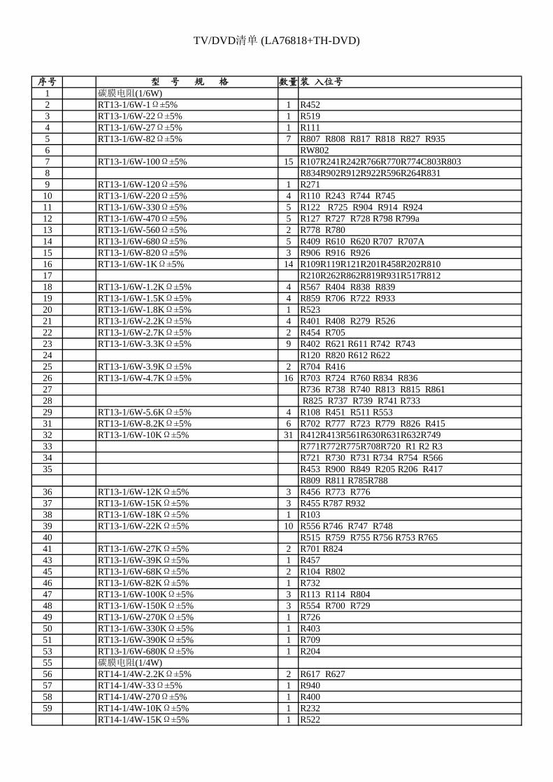
TV/DVD清单 (LA76818+TH-DVD)
序号 型 号 规 格 数量装 入位号1 碳膜电阻(1/6W)2 RT13-1/6W-1Ω±5% 1 R452 3 RT13-1/6W-22Ω±5% 1 R519 4 RT13-1/6W-27Ω±5% 1 R1115 RT13-1/6W-82Ω±5% 7 R807 R808 R817 R818 R827 R935 6 RW8027 RT13-1/6W-100Ω±5% 15 R107R241R242R766R770R774C803R8038 R834R902R912R922R596R264R8319 RT13-1/6W-120Ω±5% 1 R271 10 RT13-1/6W-220Ω±5% 4 R110 R243 R744 R745 11 RT13-1/6W-330Ω±5% 5 R122 R725 R904 R914 R924 12 RT13-1/6W-470Ω±5% 5 R127 R727 R728 R798 R799a13 RT13-1/6W-560Ω±5% 2 R778 R780 14 RT13-1/6W-680Ω±5% 5 R409 R610 R620 R707 R707A 15 RT13-1/6W-820Ω±5% 3 R906 R916 R92616 RT13-1/6W-1KΩ±5% 14 R109R119R121R201R458R202R810 17 R210R262R862R819R931R517R81218 RT13-1/6W-1.2KΩ±5% 4 R567 R404 R838 R83919 RT13-1/6W-1.5KΩ±5% 4 R859 R706 R722 R933 20 RT13-1/6W-1.8KΩ±5% 1 R52321 RT13-1/6W-2.2KΩ±5% 4 R401 R408 R279 R52622 RT13-1/6W-2.7KΩ±5% 2 R454 R705 23 RT13-1/6W-3.3KΩ±5% 9 R402 R621 R611 R742 R743 24 R120 R820 R612 R62225 RT13-1/6W-3.9KΩ±5% 2 R704 R41626 RT13-1/6W-4.7KΩ±5% 16 R703 R724 R760 R834 R83627 R736 R738 R740 R813 R815 R86128 R825 R737 R739 R741 R73329 RT13-1/6W-5.6KΩ±5% 4 R108 R451 R511 R55331 RT13-1/6W-8.2KΩ±5% 6 R702 R777 R723 R779 R826 R41532 RT13-1/6W-10KΩ±5% 31 R412R413R561R630R631R632R74933 R771R772R775R708R720 R1 R2 R334 R721 R730 R731 R734 R754 R56635 R453 R900 R849 R205 R206 R417
R809 R811 R785R78836 RT13-1/6W-12KΩ±5% 3 R456 R773 R776 37 RT13-1/6W-15KΩ±5% 3 R455 R787 R932 38 RT13-1/6W-18KΩ±5% 1 R103 39 RT13-1/6W-22KΩ±5% 10 R556 R746 R747 R748 40 R515 R759 R755 R756 R753 R76541 RT13-1/6W-27KΩ±5% 2 R701 R824 43 RT13-1/6W-39KΩ±5% 1 R45745 RT13-1/6W-68KΩ±5% 2 R104 R80246 RT13-1/6W-82KΩ±5% 1 R73247 RT13-1/6W-100KΩ±5% 3 R113 R114 R80448 RT13-1/6W-150KΩ±5% 3 R554 R700 R72949 RT13-1/6W-270KΩ±5% 1 R72650 RT13-1/6W-330KΩ±5% 1 R40351 RT13-1/6W-390KΩ±5% 1 R70953 RT13-1/6W-680KΩ±5% 1 R204 55 碳膜电阻(1/4W)56 RT14-1/4W-2.2KΩ±5% 2 R617 R62757 RT14-1/4W-33Ω±5% 1 R94058 RT14-1/4W-270Ω±5% 1 R40059 RT14-1/4W-10KΩ±5% 1 R232
RT14-1/4W-15KΩ±5% 1 R522
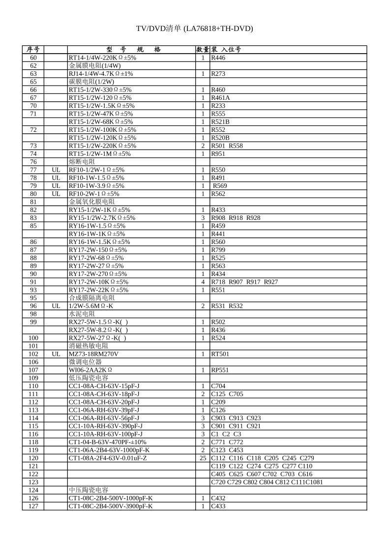
TV/DVD清单 (LA76818+TH-DVD)
序号 型 号 规 格 数量装 入位号60 RT14-1/4W-220KΩ±5% 1 R44662 金属膜电阻(1/4W)63 RJ14-1/4W-4.7KΩ±1% 1 R27365 碳膜电阻(1/2W)66 RT15-1/2W-330Ω±5% 1 R46067 RT15-1/2W-120Ω±5% 1 R461A 70 RT15-1/2W-1.5KΩ±5% 1 R23371 RT15-1/2W-47KΩ±5% 1 R555
RT15-1/2W-68KΩ±5% 1 R521B72 RT15-1/2W-100KΩ±5% 1 R552
RT15-1/2W-120KΩ±5% 1 R520B73 RT15-1/2W-220KΩ±5% 2 R501 R55874 RT15-1/2W-1MΩ±5% 1 R95176 熔断电阻77 UL RF10-1/2W-1Ω±5% 1 R55078 UL RF10-1W-1.5Ω±5% 1 R491 79 UL RF10-1W-3.9Ω±5% 1 R56980 UL RF10-2W-1Ω±5% 1 R56281 金属氧化膜电阻82 RY15-1/2W-1KΩ±5% 1 R433 83 RY15-1/2W-2.7KΩ±5% 3 R908 R918 R92885 RY16-1W-1.5Ω±5% 1 R459
RY16-1W-1KΩ±5% 1 R44186 RY16-1W-1.5KΩ±5% 1 R56087 RY17-2W-150Ω±5% 1 R79988 RY17-2W-68Ω±5% 1 R52589 RY17-2W-27Ω±5% 1 R563 90 RY17-2W-270Ω±5% 1 R43491 RY17-2W-10KΩ±5% 4 R718 R907 R917 R92793 RY17-2W-22KΩ±5% 1 R55195 合成膜隔离电阻96 UL 1/2W-5.6MΩ-K 2 R531 R532 98 水泥电阻99 RX27-5W-1.5Ω-K( ) 1 R502
RX27-5W-8.2Ω-K( ) 1 R436100 RX27-5W-27Ω-K( ) 1 R524101 消磁热敏电阻102 UL MZ73-18RM270V 1 RT501106 微调电位器107 WI06-2AA2KΩ 1 RP551109 低压陶瓷电容110 CC1-08A-CH-63V-15pF-J 1 C704 111 CC1-08A-CH-63V-18pF-J 2 C125 C705112 CC1-08A-CH-63V-20pF-J 1 C209113 CC1-06A-RH-63V-39pF-J 1 C126 114 CC1-06A-RH-63V-56pF-J 3 C903 C913 C923115 CC1-10A-RH-63V-390pF-J 3 C901 C911 C921116 CC1-10A-RH-63V-100pF-J 3 C1 C2 C3118 CT1-04-B-63V-470PF-±10% 2 C771 C772119 CT1-06A-2B4-63V-1000pF-K 2 C123 C453 120 CT1-08A-2F4-63V-0.01uF-Z 25 C112 C116 C118 C205 C245 C279121 C119 C122 C274 C275 C277 C110122 C405 C625 C607 C702 C703 C616 123 C720 C729 C802 C804 C812 C111C1081124 中压陶瓷电容126 CT1-08C-2B4-500V-1000pF-K 1 C432127 CT1-08C-2B4-500V-3900pF-K 1 C433

TV/DVD清单 (LA76818+TH-DVD)
序号 型 号 规 格 数量装 入位号129 高压陶瓷电容130 CT81-08C-2R-1KV-470pF-K 1 C554 131 CT81-06C-2R-1KV-1000pF-K 4 C503 C504 C505 C506132 CT81-10C-2R-2KV-680pF-K 1 C438 (配DC11偏转为1000P)133 CT81-10C-2R-2KV-470pF-K 3 C551 C552 C516134 CT81-12C-2R-2KV-1000pF-K 1 C939135 UL CT81-AC400V-470PF-K 1 C532136 UL CT81-AC400V-2200PF-M 1 C533138 电解电容139 CD110-10V-470uF -M 2 C570 C572140 CD110-16V-2.2uF -M 4 C104 C714 C615 C626141 CD110-16V-10uF -M 26 C276 C931 C932 C610 C611 C620142 C621 C773 C774 C803 C806 C807143 C808 C809 C810 C811 C813 C814144 C822 C1080145 C815 C816 C831 C832 C833 C834146 CD110-16V-47uF -M 5 C244 C278 C701 C719 C206 147 CD110-16V-100uF -M 8 C115 C623 C613 C614 C101148 C624 C631 C404149 CD110-16V-220uF -M 4 C801 C592 C576 C598150 CD110-16V-470uF -M 1 C805151 CD110-16V-1000uF -M 3 C594 C595 C593152 CD110-25V-100uF -M 1 C565153 CD110-50V-2.2uF -M 1 C456154 CD110-25V-470uF -M 2 C622 C612155 CD110-25V-1000uF -M 1 C564 156 CD110-25V-2200uF -M 2 C457 C606157 CD110-35V-47uF -M 2 C434 C414158 CD110-35V-100uF -M 1 C451159 CD110-35V-470uF -M 1 C563 160 CD110-35V-1000uF -M 1 C452161 CD110-50V-0.22uF -M 1 C402162 CD110-50V-0.47uF -M 6 C137 208 401 403 210 934164 CD110-50V-1uF -M 10 C117 C211 C139 C204 C713 165 C407 C454 C213 C861 C415166 CD110-50V-4.7uF -M 2 C203 C708
CD110-50V-100uF -M(Φ8X12) 1 C450167 CD110-160V-1uF -M 1 C444168 CD110-160V-470uF -M 1 C561
CD110-250V-4.7uF-M 1 C951169 CD110-250V-22uF-M 1 C562170 CD293-400V-220uF-±10% 1 C507171 无极性电解电容172 CD71-BP-50V-2.2uF-M 2 C617 C627173 CD71-BP-50V-1uF-M 1 C231 175 聚酯膜电容177 CL11-63V-0.015uF-K 2 C515 C517178 CL11-63V-0.022uF-K 1 C120 179 CL11-63V-0.033uF-K 2 C124 C406
CL11-63V-0.047uF-K 1 C121 180 CLX-100V-0.1uF-±5% 4 C459 C207 C408 C514 181 CL12-100V-0.033uF-K 1 C458182 CL21X-100V-0.47uF-±5% 1 C437184 金属聚酯膜电容185 UL 275V AC-0.22uF--K 2 C501 C502187 高压聚丙烯电容188 CBB81-1.6KV-9100PF-±5% 1 C435
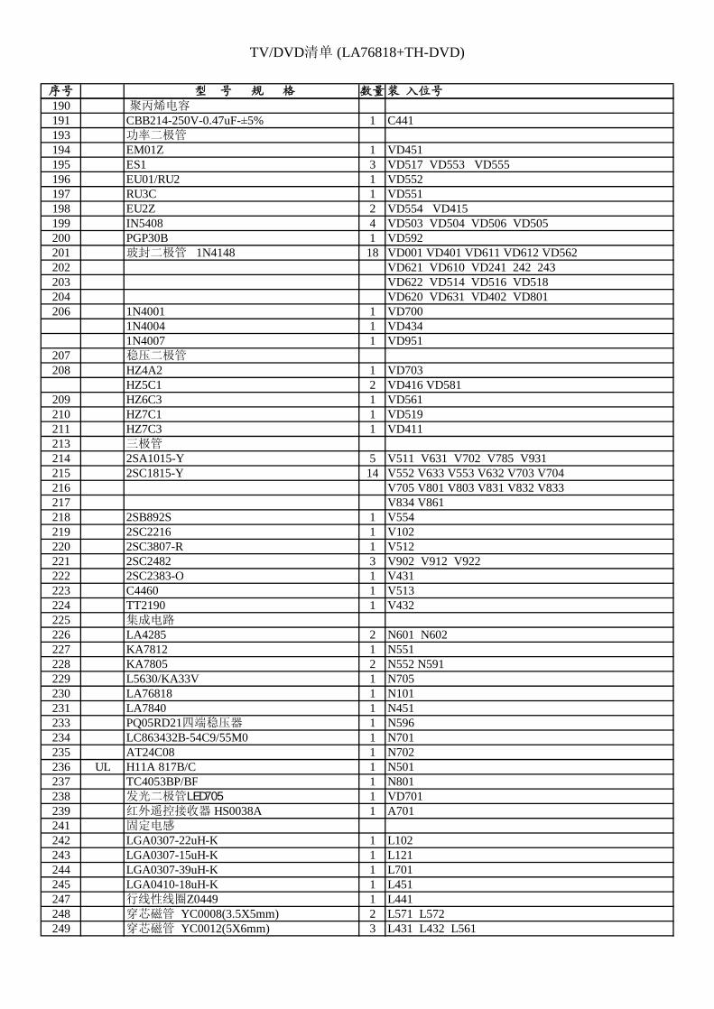
TV/DVD清单 (LA76818+TH-DVD)
序号 型 号 规 格 数量装 入位号190 聚丙烯电容191 CBB214-250V-0.47uF-±5% 1 C441193 功率二极管194 EM01Z 1 VD451195 ES1 3 VD517 VD553 VD555 196 EU01/RU2 1 VD552197 RU3C 1 VD551198 EU2Z 2 VD554 VD415199 IN5408 4 VD503 VD504 VD506 VD505200 PGP30B 1 VD592201 玻封二极管 1N4148 18 VD001 VD401 VD611 VD612 VD562 202 VD621 VD610 VD241 242 243203 VD622 VD514 VD516 VD518204 VD620 VD631 VD402 VD801206 1N4001 1 VD700
1N4004 1 VD4341N4007 1 VD951
207 稳压二极管208 HZ4A2 1 VD703
HZ5C1 2 VD416 VD581209 HZ6C3 1 VD561 210 HZ7C1 1 VD519 211 HZ7C3 1 VD411213 三极管214 2SA1015-Y 5 V511 V631 V702 V785 V931215 2SC1815-Y 14 V552 V633 V553 V632 V703 V704 216 V705 V801 V803 V831 V832 V833 217 V834 V861 218 2SB892S 1 V554 219 2SC2216 1 V102220 2SC3807-R 1 V512 221 2SC2482 3 V902 V912 V922222 2SC2383-O 1 V431223 C4460 1 V513224 TT2190 1 V432225 集成电路226 LA4285 2 N601 N602227 KA7812 1 N551228 KA7805 2 N552 N591229 L5630/KA33V 1 N705230 LA76818 1 N101231 LA7840 1 N451233 PQ05RD21四端稳压器 1 N596234 LC863432B-54C9/55M0 1 N701235 AT24C08 1 N702236 UL H11A 817B/C 1 N501237 TC4053BP/BF 1 N801238 发光二极管LED705 1 VD701239 红外遥控接收器 HS0038A 1 A701241 固定电感242 LGA0307-22uH-K 1 L102243 LGA0307-15uH-K 1 L121244 LGA0307-39uH-K 1 L701 245 LGA0410-18uH-K 1 L451247 行线性线圈Z0449 1 L441248 穿芯磁管 YC0008(3.5X5mm) 2 L571 L572 249 穿芯磁管 YC0012(5X6mm) 3 L431 L432 L561

TV/DVD清单 (LA76818+TH-DVD)
序号 型 号 规 格 数量装 入位号250 磁管 Z2073 2 V513 V432252 跳线 TXP-5mm 11 W102,121,204,562,618,253 W723,L511254 W503(手插)W003,C601,C602255 跳线 TXP-7.5mm 66 W103,104,106,107,108,118,201,202,203,256 W207,210,402,413,471,R270,208,403,801,257 W409,410,411,412,414,417,426,429,430,258 W438,440,451,510,555,607,609,610,259 W611,612,703,704,711,716,717,260 W718,719,720,721,737,740,744,743,746,261 W755,756,762,792,795,804,807,809,815,262 W512,852,WR280263 W552,734,264 W902270 跳线 TXP-10mm 56 W109,111,113,116,120,205,271 W216,217,265,271,406,407,408,272 W415,416,420,441,473,507,615,273 W515,551,569,603,605,608,702,705,706,274 W707,708,709,710,712,713,714,722,724,275 W725,726,727,728,729,731,738,715276 W739,752,753,761,803,805,861277 W405278 W901,L901284 跳线 TXP-12.5mm 10 W404,421,502,554,578,579,285 W602,604,771,772,701287 跳线 TXP-15mm 17 W418,443,422,R434A,442,501,553,561560288 W617,735,741,742,745,750,793,794291 跳线 TXP-20mm 3 W747 W748 W749293 UL 消磁线圈 CDLX--37 1 L909 294 UL 继电器 HKE HRMH-S-DC12V-A 1 RL551
声表面F45C 1 Z101295 中频线圈 ST6017 1 T101296 UL 行输出CF0801-4703/XF0801-01CK01 1 T471297 UL 开关变压器 BCK-100-02L(绝缘等级E)E 1 T511298 UL 电源滤波器 LG-003-NL 2 L501 L502299 行推动变压器 TX40 1 T431301 S-VIDEO输入插座 SW-3K 1 XS805302 6孔AV组件 AV3-6(上红,中白,下黄) 1 XS801303 轻触开关 KFC-A06-H5.0 10 SW701 SW702 SW703 SW707 POWER304 SW704 SW705 SW706 SW708 SW709305 UL 像管座GZS12-4-AC 1306 UL 保险管 50T T3.15A 250V AC 1 FU501 307 调谐器FTDC3Y13MV04 1 A101 308 石英振荡器 JA18B-4.4336169MHz 1 G201309 陶瓷振荡器 32.768KHz 1 G701310 UL 电源线 NISPT-2 18AWGX2C VW-1 DTI-2P-02 1 U902VDE/UL 美式二极扁插(带VH-3Y)
UL 插头插座(电源线) 1 VH-3Y(插头) VH-3A(插座)311 喇叭YDT5090-20-5W-8Ω 2 B901 B902312 UL 印制板(主板) DAP7.820.588B 1313 UL 印制板(遥控板)DAP7.820.580A 1314 UL 印制板(按健板)DAP7.820.579 1315 UL 印制板(视放板)DAP7.820.570A(彩虹管) 1316 UL 印制板(AV 板)DAP7.820.478 1317 遥控发射器 CDL-78 1320 UL 显像管 1321 DVD机芯(含解码板)DV34-78LA 1
DCL34MK89D Complete Loader
Service Manual


5
5
4
4
3
3
2
2
1
1
D D
C C
B B
A A
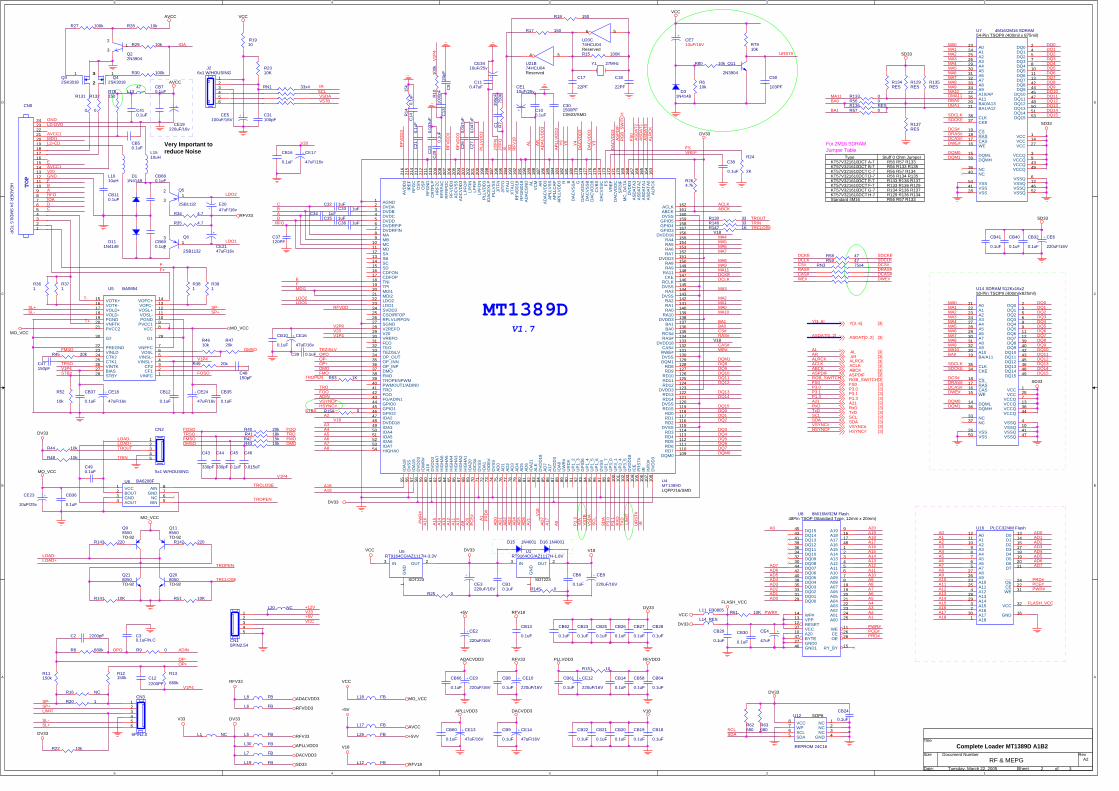
Sanyo slim HD60 PUH1 INDEX
ASPDIF Output Signal
System Configuration
MT1389D Pin 167
EAUXx
SCART Control Signal RGB/Video Switch.
3 AUDIO DAC DA1196 & VIDEO OUT
MT1389D Pin 82 A21
MT1389D Pin 170MT1389D Pin 169
FUNCTION
MT1389D (LQFP216) DVD Complete Loader for
MT1389D Pin 100 P3.1MT1389D Pin 99 P3.0
General Purpose I/O
SCART Control Signal FS0.
2 MPEG & MEMORY, FLASH - MT1389D
& STEREO OUTPUT NO DAC & 4558 & MUTE
MT1389D Pin 92 P1.3 General Purpose I/O.General Purpose I/O.General Purpose I/O.
MT1389D Pin 161 ABCKMT1389D Pin 162 ACLKMT1389D Pin 163 ALRCK
General Purpose I/O If No 5.1 ChannelGeneral Purpose I/O If No 5.1 ChannelAudio Output MUTE Control signal If No 5.1 Channel
INDEX A4
Complete Loader MT1389D A1B2
1 3Tuesday, March 22, 2005
Title
Size Document Number Rev
Date: Sheet of
5
5
4
4
3
3
2
2
1
1
D D
C C
B B
A A
KT57V321610DCT F-7
Type
R56 R57 R134
KT57V321610DCT E-7
KT57V321610DCT A-7
V1.7
R56 R134 R135
KT57V321610DCT B-7 R56 R133 R135
KT57V321610DCT G-7KT57V321610DCT H-7
R56 R57 R133
Standard 4M16
KT57V321610DCT C-7KT57V321610DCT D-7
Stuff 0 Ohm Jumper
Very Important toreduce Noise
R133 R136 R137
R56 R57 R133
For 2M16 SDRAMJumper Table
R133 R136 R129R134 R136 R137R129 R136 R134
RF & MEPG A2
Complete Loader MT1389D A1B2
2 3Tuesday, March 22, 2005
Title
Size Document Number Rev
Date: Sheet of
D
DQ1
SDCKE
A9
DQM0
DQ9
MA11
FOSO
ADIN
A14
DWE#
DQ8
A3
DQ12
A19
SP+
A14
AD
5
A8
V2P8
LDO1
RAS#
DQ15
MA6
A17
DA
CV
DD
3
LOAD-
PLL
VD
D3
OPO
DCKE
A16
V18
DQ6
AD3
DQ10
RG
B_S
WIT
CH
DMA11
DQ3
MA7
DQ15
MA5
RGB_SWITCH
AD4
TRCLOSE
A6
BA1
A15
Y5
DQ7
MA3
DQ1
SDCKE
A11
AD
6
A18
A2
RFO
V18
FMO
OP+
P3.0
V33
A17
A6
A18
FOO
TRIN
A5
DWE#
RFVDD
B
DQ3
TROPEN
TRSO
DCAS#
MA9
BA1
SP+
STBY TxD
A10
DMSO
ADIN
A9
A
SP-
V1P
4
AVCC1
A9
A
LD-CD
AD
2
WE#
C
PCE#
A17
DQ5
A0
MA6
JITF
N
DQM1
SDCLK
TRO
SL+
A1
F
ALRCK
DCLK
AD
0
A21
AD3
MA1
A20
DCS#
ABCK
DQ13
A7
OPO
DBA1
MA10
MA9
TRIN
FMSO
FLASH_VCC
MA10
DQ0
AR
AD
3
A1
MA2
VS
TB
E
DQ10
MA0
C
MA4
FS0
DQ4
SDCLK
A16
DCAS#
MA8
MDI1
DQ7
HSYNC#
A8
AD1
DQ4
A1
FMO
AS
DA
T1
XO
V18
DQ4
DRAS#
DQ3
AD0
IRLIM
IT
A15
DQM1
PWR#
SL+
VREF
MA0
T-
DQM1
ALR
CK
ABCK
DQ11
BA0
DQ13
PCE#
V1P4
AD2
A2
DRAS#
A10
IR
Y4
DQ9
V20
B
A13
RxD
AD0
AD4
CAS#
DQ9
A16
ASDAT[0..2] MA7
DQ14
XI FS
RX
DA
SP
DIF
A4
MA6
CS#
SD
A
FOSO
AD
1
MA3
A20
UR
ST#
ACLKDQ14
DQ11
DQ8
SDA
TXD
PWR#AD2
AS
DA
T0
F-
MA2
DQ6
TEZISLV
TRO
A4
DCS#
V20AVCC1
FOO
FMSO
A12
DQM0
V18
A2
ACLK
A10
ASPDIF
OP+
AD
7
FS0
P3.
1
E
P3.1
DQ10
DQ5
DMSO
A5
A6
A12
PWR#
PRD#
RFV
DD
3
DQ5
LD-DVD
V1P4
AL
RFV
DD
3
AD6
DQ2
A8
A19
RFV
18
TROUT
Y[3..6]
A0
DQ6
V20
A7
TRCLOSE
AS
DA
T2
V1P4
DQM0
DQ2
MA9
F
AL
LIMIT
MA0
A12
AD5
A7
PC
E#
DQ0
VCC
DQ15
MA11
DQ14
MDI1
STBY
A0
MA4
MA2
A3SDA
VSYNC#
DQ11
SP-
P3.
0
A11
DA
CV
DD
3
DQ12
Y6
V1P4
A4
Y3
AR
MA3
DQ12
V1P4
TROUT
PRD#
A13
A14
DQ13
A5
DQ2
MA1
DBA0
SC
L
AP
LLV
DD
3
T+
PR
D#
AD
4
D
OP-
AD7
DQ7
A13
A15
LDO2
AD7
MA1
VSDA
F+
LOAD+
A21
AD6
DQ1
IOA
DQ8
IOA
MA5
MA7
SL-
JITF
O
DA
CV
DD
3
P1.3
AD1
VS
DA
MA8
RFO
DMO
OP-
A18
+5V
A11AD5
DQ0
MA4
P1.
3
DMO
SCL
BA0
MA8
MA10
LDO2
SL-
MA5
A3A
DA
CV
DD
3
LDO1
BA0
PW
R#
LOAD-
TRCLOSE
TROPENLOAD+
+12V
TRSO
RFV
DD
3
SCL
SCL
VSTB
GND
GND
CS# DCS#DRAS#DCAS#DWE#
RAS#CAS#WE#
DCKEDCLK SDCLK
SDCKE
TROPEN
IOA
HSYNC#VSYNC#
URST#
RxD [3]
ASPDIF [3]
ASDAT[0..2] [3]
A21 [3]
AL [3]
RGB_SWITCH[3]
P1.3 [3]
ABCK [3]
P3.1 [3]
AR [3]
TxD [3]
P3.0 [3]
ALRCK [3]
SCL [3]
ACLK [3]
Y[3..6] [3]
SDA [3]
FS0 [3]
HSYNC# [3]VSYNC# [3]
DV33
PLLVDD3
SD33
VCC
SD33
MO_VCC
V18
ADACVDD3
FLASH_VCC
RFV33
MO_VCC
SD33
RFV33
DACVDD3
RFV33
SD33
RFVDD3
VCC
APLLVDD3
DACVDD3
VCC
DV33
RFVDD3
AVCC
SD33
V18
AVCC
DV33
DV33
RFV18
DV33
DV33
RFV33
AVCC
APLLVDD3
DV33
ADACVDD3
DV33
+5V
MO_VCC
V33
MO_VCC
VCC
MO_VCC
RFV18
DV33 V18VCC
+5VV
+5V
R41 18k
C39 0.1uF
C43
330pF
U1RT9164CG/AZ1117H-1.8V
SOT223
1
23
GN
D
OUTIN
R49 20k
R13
680k
C48150pF
+
CE110uF/25v
R35 4.7
+ CE10
220uF/16V
R30 100k
+ CE2
220uF/16V
+ CE16
47uF/16v
CB8
0.1uF
R45 20k
CB28
0.1uF
CB22
0.1uF
CB27
0.1uF
+ CE8
220uF/16V
R264.7k
Q22N3904
13
2
CB6
0.1uF
D11N4148
R4610k
J26x1 W/HOUSING
123456
L19 FB
+
CE3220uF/16V
RN3 75x4
CB10.1uF
C29
0.1u
F
R20 1
R80 10k
R16 NC
C47150pF
R9 0
C34 1uF
R7
750k
R27 100k
C50
103PF
C2 2200pF
R131
0
R51 10K
R48 10k
+ CE17
47uF/16v
C37120PF
L26 FB
R132
0
CB62
0.1uF
U6 BA6208F1234 5
678VCC
BOUTGNDAOUT BIN
NCGNDAIN
CN3
6PIN2.0
123456
CN2
5x1 W/HOUSING
12345
C46
0.015uF
R141 10K
CB10
0.1uF
R11150k
D111N4148
+ CE13
47uF/16V
C1
390p
F
L7 FB
R43 10k
CB60
0.1uF
CB690.1uF
R8 680k
CB680.1uF
R78150
+ CE6
220uF/16V
CB20
0.1uF
C122200PF
+CE5100uF/16V
CB25
0.1uF
CB41
0.1uF
+ CE18
47uF/16v
+
CE3410uF/25v
+ CE9
220uF/16V
R361
+CE23
10uF/25v
CB66
0.1uF
R10
100k
CB37
0.1uF
R391
C38
0.1uF
CB32
0.1uF
L6 FB
CB40
0.1uF
CB21
0.1uF
CB12
0.1uF
L20 NC
C35 1uF
CB14
0.1uF
R28 10k
C490.1uF
Q98550TO-92
R4720k
Q218050TO-92
U5 BA5954
1
910
12
32
15
7
1413
21
1920
24
27
6
45
28
8
111718
16
2322
2526
2930
VINFC
PVCC1PGND
VOSL+
CF2CF1
VOTK+
VNFFC
VOFC+VOFC-
PVCC2
PGNDVNFTK
CTK2
BIAS
VOSL
VINSL+VINSL-
STBY
VCC
VOSL-VOLD+VOLD-
VOTK-
VINLDPREGND
CTK1VINTK
G1G2
C100.1uF
R151 10
CB18
0.1uF
C21
0.1u
F
CB13
0.1uF
Q5
2SB1132
13
2
R29 10k R7910k
CB16
0.1uF
C45
0.1uF
C301500PFC0603/SMD
C30.1uF/N.C
C23
0.03
3uF
L30 FB
R130 33
C8
20pF
R146 33
R40 20k
R147 1K
R2310K
C110.47uF
L1 NC
L18 FB
Q118550TO-92
R1910
RN1 33x4
CB50.1uF
R134RES
R133 0
R17 150
R129RES
U20C74HCU04Reserved
56
R57 0
C18
22PF
C17
22PF
R15 100K
Y1 27MHz
L12 FB
U7 4M16/2M16 SDRAM54-Pin TSOPII (400mil x 875mil)
1
24
12
57
9
810
46
1113
15
16171819
3522
23242526
14
41
293031323334
36
3738
39
40
43
4244
52
4547
49
48505153
54
2021
3
6
27
28
VCC
DQ0DQ1
VSSQ
DQ2DQ3
VCCQ
DQ4DQ5
VSSQ
DQ6DQ7
DQML
WECASRASCS
A11A10/AP
A0A1A2A3
VCC
VSS
A4A5A6A7A8A9
NC
CKECLK
DQMH
NC
VCCQ
DQ8DQ9
VSSQ
DQ10DQ11
VCCQ
DQ12DQ13DQ14DQ15
VSS
BA0/A13BA1/A12
VCCQ
VSSQ
VCC
VSS
Q42SK3018
13
2
U5RT9164CG/AZ1117H-3.3V
SOT223
1
23
GN
D
OUTIN
R18 150
R136 RES
R53 1K
R135RES
U21B74HCU04Reserved
34
R137RES
R145 0
R58 47
R56 0
CB110.1uF
C13
1000
pF
R59 47
+ E2047uF/16v
R381
R14
15k
MT1389D
U4MT1389DLQFP216/SMD
2
210
345
1
212
213
6789
1011121314151617181920212223
216
2827
3029
3231
43
2625
33343536
4241
45
3940
46
3837
65646261605958
52
81777655 7473727163 83
5354
7057 827566 68 806956 67 84 85 86 87 88 89 90 91 92 93 94 95 106
96 97
204
205
98 99 100
101
102
103
104
105
107
108
162161160159158157156155154153152151150149148147146145144143142141140139
137138
136135134133132131130129128
126127
125124123122121120
118119
117116115114113
111112
110109
209
215
24
214
191
190
198
197
208
207
196
211
206
203
201
202
200
199
194
195
192
184
185
182
181
180
179
186
178
177
175
173
174
164
171
170
169
168
172
167
166
165
163
193
44
4748495051
78 79
176
183
188
189
187
DVDA
CR
TPLP
DVDBDVDCDVDD
AGND
OS
PO
SN
DVDRFIPDVDRFINMAMBMCMDSASBSCSDCDFONCDFOPTNITPIMDI1MDI2LDO2LDO1
AV
DD
3
V2REFOSGND
VREFOV20
TEOFEO
FG/ADIN1
RFLVL/RFONCSO/RFOP
TEZISLVOP_OUTOP_INNOP_INP
FOOTRO
GPIO1
TROPENPWMPWMOUT1/ADIN0
GPIO2
FMODMO
HIG
HA
4H
IGH
A5
HIG
HA
7D
VD
D3
A16
IOW
R#
DV
DD
3
IOA6
AD
6
AD
2A
D1
IOA
18
DV
SS
IOO
E#
IOA
1D
VS
S
HIG
HA
6
ALE
IOA7HIGHA0
IOC
S#
IOA
19
IOA
21
AD
0
HIG
HA
3
HIG
HA
1
AD
5
IOA
20
DV
SS
HIG
HA
2
DV
DD
18A
D7
A17
DV
DD
3IO
A0
UW
R#
UR
D#
UP
1_2
UP
1_3
GP
IO6
UP
1_4
UP
1_5
IRUP
1_6
DV
SS
AD
CV
DD
3A
DC
VS
S
UP
1_7
UP
3_0
UP
3_1
UP
3_4
UP
3_5
DV
DD
18IC
EP
RS
T#
INT0
#D
VD
D3
ACLKABCKDVSS
GPIO5GPIO4GPIO3
DVDD18RA4RA5RA6RA7
DVDD3RA8RA9
RA11CKE
RCLKDVSS
RA3DVSS
RA2RA1RA0
RA10
BA1DVDD3
BA0RCS#RAS#
DVDD18CAS#RWE#DVSSDQM1
RD8
RD10RD9
RD11RD12
DVDD3RD13RD14DVSS
RD0RD15
RD1RD2
DVSSRD3RD4
RD6RD5
RD7DQM0
HR
FZC
IRE
F
SVDD3
RFG
C
RFG
ND
18A
DA
CG
ND
IDA
CE
XLP
PLL
VS
S
RFR
PA
CR
FRP
DC
JITF
N
RFG
ND
RFV
DD
3
LPFO
P
LPFI
PLP
FIN
LPFO
NP
LLV
DD
3
XTA
LIJI
TFO
RFV
DD
18
AP
LLC
AP
AP
LLV
SS R B
DA
CV
SS
A G
AD
AC
VD
D3
DA
CV
DD
AD
AC
VS
SB
CV
BS FS
DA
CV
SS
C
AS
DA
TA0
DA
CV
DD
CS
PD
IFM
C_D
ATA
DV
DD
3
VR
EF
AS
DA
TA3
AS
DA
TA2
AS
DA
TA1
ALR
CK
XTA
LO
GPIO0
IOA2DVDD18IOA3IOA4IOA5
AD
3A
D4
DA
CV
DD
B
AP
LLV
DD
3
VC
MAL
AR
+
CE2147uF/16v
C44
330pF
C33 1uF
CN15PIN2.54
12345
R34 4.7
R12150k
CB23
0.1uF
C31100pF
L1510uH
CB35
0.1uF
C410.1uF
R44 10k
CB30
0.1uF
CB29
0.1uF
L11 FB0805
+CE4
47uF
L14 RES
Q11
2N3904
R371
Q6
2SB1132
13
2
R25 0
L1610uH
R143 220
R61 10K
L17 FB
C14
0.1u
F
U8 8M/16M/32M Flash48Pin TSOP (Standard Type, 12mm x 20mm)
37
2746
45434139363432304442403835333129
15
9161748123456781819202122232425
1211
472628
1314
10 VCC
GND0GND1
DQ15DQ14DQ13DQ12DQ11DQ10DQ09DQ08DQ07DQ06DQ05DQ04DQ03DQ02DQ01DQ00
RY_BY
A19A18A17A16A15A14A13A12A11A10A09A08A07A06A05A04A03A02A01A00
RESETWE
BYTECEOE
VPPWP#
A20
R142 220
CB70.1uF
CB64
0.1uF
D31N4148
R24
2K
R610k
L8 FB
C32 1uF
CB58
0.1uF
R150 0
+CE710uF/16V
CB19
0.1uF
U14 SDRAM 512Kx16x250-Pin TSOPII (400milx825mil)
1
23
4
56
7
89
10
1112
1314
15161718
1920
21222324
25
26
272829303132
33
3435
36
37
38
3940
41
4243
44
4546
47
4849
50
VCC
DQ0DQ1
VSSQ
DQ2DQ3
VCCQ
DQ4DQ5
VSSQ
DQ6DQ7
VCCQDQML
WECASRASCS
BA/A11A10
A0A1A2A3
VCC
VSS
A4A5A6A7A8A9
NC
CKECLK
DQMH
NC
VCCQ
DQ8DQ9
VSSQ
DQ10DQ11
VCCQ
DQ12DQ13
VSSQ
DQ14DQ15
VSS
L1347
CB24
0.1uFU12
EEPROM 24C16
SOP812345
678 NC
NCNC
GNDSDASCLWPVCC
+ CE24
47uF/16v
R22 10k
+ CE12
220uF/16V
R62680
CB61
0.1uF
+ CE14
47uF/16V
R63680CB9
0.1uF
U16 PLCC32/4M Flash12111098765
272623254
282932
301
31
1314151718192021
32
16
2224
A0A1A2A3A4A5A6A7A8A9A10A11A12A13A14A15A16A17A18
WE
D0D1D2D3D4D5D6D7
VCC
GND
CEOE
CB36
0.1uF
TOP
CN5
HE
AD
ER
24 SM
D0.5 TO
P 123456789101112131415161718192021222324
+
CE19220uF/16v
CB26
0.1uF
C27
0.04
7uF
R42 15k
C26
0.04
7uF
R52
10k
D16 1N4001D15 1N4001
Q208050TO-92
C36 1uF
L5 FB
Q32SK3018
1 3
2
5
5
4
4
3
3
2
2
1
1
D D
C C
B B
A A
E
Hardware Control Mode24Bit-I2S Format
3906
Hardware Control ModeI2S Format
B
C
VIDEO & AUDIO OUTPUT A3
Complete Loader MT1389D A1B2
3 3Tuesday, March 22, 2005
Title
Size Document Number Rev
Date: Sheet of
SDAT0
SABCK
SL
MICM
SR
LFE
Y4Y4
LFE
CVBS#
SALRCK
Y3Y3
LFE
ASPDIF
Y6Y6
CENTSL
MUTE
SDAT2
CVBS#
SDAT2
CVBS_ST
SDAT1
SR
SR
MLML
CENT
MR
CVBS_ST
ML
Y5Y5
MR
SL
MR
CENT
SACLK
SDAT1
ASDAT1ASDAT2
MR
G/Y
MUTE
A_MUTE
ML
A_MUTE
MR
A_MUTE
AR
AL
ACLK
ASDAT0
ABCK
ALRCK
ALRCK
SACLKSABCKSALRCKSDAT0
ABCKACLK
ALRCK
A_ACLKM_MUTEMUTE
ML
SLSRCENTLFE
G/YB/U(SC)
R/V(SY)
FS0RGB_SWITCHASPDIF
R/V(SY)
B/U(SC)
P3.1
P3.0
A_ABCK
P3.1
P1.3
A_ACLK
P3.0
A21
P1.3A21
ALRCK
FS0_[2]
[2]_Y3
ASDAT0
RxD_[2]
ASDAT2
ABCK
P3.1_[2]
TxD_[2]
[2]_Y5
ACLK
[2]_Y4
P1.3_[2]
[2]_AR[2]_AL
[2]_Y6
ASDAT1
A21_[2]
HSYNC#_[2]
SDA_[2]SCL_[2]
VSYNC#_[2]
ASPDIF
RGB_SWITCH_[2]
P3.0_[2]+5VV
+5V
AVDD
DV33
VCC
DVDD
+5VV
+5VV
DVDD AVDD
AVCC
+5VV
+5VV
+5V
VREF
+12V
A+9V
VREF
VREF
AF+12V
VREF
VREF
+5VV
DV33
VCC
CF2
22PF
R11675,1%
CF16
22PF
CF15
22PF
CF18
22PF
CF17
22PF
R72 1K
R87 33
R704.7
+
-
U10B358
5
67
R88 33
R1521kR0603/SMD
C7
47P
+
-
U10A358
3
21
48
R115
75,1%
CB48
0.1uF
Q133906
Q73906
Q83904
12
3R68 1K
R5510K
R671K
R12810K
+ CE32
220uF
R13910K
R13810K
Q13906
+CE11
47uF
L27 FB0805
U12 WM8766/WM8772
SSOP28DA1166/DA1172
1
234
5
6
789
10
1112
1314
15
16
1718
1920
2122
2324
2526
27
28MODE
MCLKBCLKLRC
DVDD
DGND
DIN1DIN2DIN3
DOUT
ML/I2SMC/IWL
MD/DMMUTE
TESTREF1
VREFN
VFEFPVMID
AINRAINL
VOUT1LVOUT1R
VOUT2LVOUT2R
VOUT3LVOUT3R
AGND
AVDD
CB4
0.1uF
+ CE33
220uF
Q9
39041
2
3
C91
0.1uF
C77
0.1uF
+CE48
10uF
CB55
0.1uF
Q103904
12
3
+CE28
220uF
CF5
22PF
CF6
22PF
CB57
0.1uF
CB47
0.1uF
R74 1K
L21 NC
+CE27
220uF
CN7
PITCH=2.0M/M123456789
1011121314
+
CE30 10uF
+CE29
10uF
R73 1K
L28 FB0805
L3 1.8uH
C5
47P
+
CE31 10uF
U6 KHTech DA1196/WM8746SSOP-28
6 CH DAC for DCL34MK-75
1
11
121314
9
8
10
234567
1528
2024
262218
27
25
23
21
19
17
16
DVDD
DGND
LATCH/12SSCLK/IWLSDIN/DM0
MUTE
MODE
LRCLK2
MCLKBCLKLRCLKDIN0DIN1DIN2
AVDD1AVDD2
AGND1AGND2
GR0GR1GR2
OUT0R
OUT0L
OUT1R
OUT1L
OUT2R
OUT2L
CAP
CN6PITCH=2.0M/M
123456789
10111213Q17
3906
L9 1.8uH
CB54
0.1uF
C19
47P
C20
47P
L10 1.8uH
CB49
0.1uF
R60
4.7K
+ CE25
47uF
R54 4.7K
CB50
0.1uF
R117
75,1%
R153 NC
CB67
0.1uF
CB2
0.1uF
CN8
PITCH=2.0M/M
123456789
101112131415
C91 0.1u
R3 20k
R32 10k
C255
1000PF
+
CE29 10u
R110150,1%
R4100K
R1 5.1k
R5100K
C24
100PF
C221000PF
C9
47P
R31 20k
CB56
0.1uF
R2 10k
+
CE15 10uF
+
CE22 10uF
Q183906
R33 5.1k
C40
100PF
R149 0R76 0
R75 0
R118
75,1%
R71 1K
R109150,1%
R2610K
R7710K
CF12
22PF
CF7
22PF
CF14
22PF
R6510K
CF13
22PF
CF8
22PF
Q193906
CF10
22PF
R114150,1%
CF9
22PF
R154 NC
C28
47P
CF11
22PF
C6
47P
RN5 33x4
R127
75,1%
R108150,1%
R64 10K
R6610K
R691K
C4
47PF
L2 1.8uH
C15
47PF
CF1
22PF
CF3
22PF
CF4
22PF
Q143906

Item Value Part No Package Quantity Vender Note
1 0 Ohm 1/16W ±5% SR2-000016-J SMD 0603 9 R9 R25 R56 R57 R131 R132 R133 R145 R150
2 1 Ohm 1/16W ±5% SR2-1R0016-J SMD 0603 5 R20 R36 R37 R38 R39 3 4.7Ohm 1/16W ±5% SR2-4R7016-J SMD 0603 3 R34 R35 R704 10 Ohm 1/16W ±5% SR2-100016-J SMD 0603 2 R19 R1515 33 Ohm 1/16W ±5% SR2-330016-J SMD 0603 5 R53 R75 R130 R146 R1476 33 Ohm X 4 ±5% Resistor Array SR6-330016-J MNR04 2 RN1 PN37 75 Ohm 1/16W ±5% SR2-750016-J SMD 0603 7 R58 R59 R115 R116 R117 R118 R127 8 100 Ohm 1/16W ±5% SR2-101016-J SMD 0603 4 R17 R18 R73 R749 150 Ohm 1/16W ±5% SR2-151016-J SMD 0603 4 R108 R109 R110 R114
10 220 Ohm 1/16W ±5% SR2-221061-J SMD 0603 3 R80 R142 R14311 680 Ohm 1/16W ±5% SR2-681016-J SMD 0603 3 R62 R63 R7812 1K Ohm 1/16W ±5% SR2-102016-J SMD 0603 5 R67 R68 R69 R71 R7213 2K Ohm 1/16W ±5% SR2-202016-J SMD 0603 1 R2414 5.1K Ohm 1/16W ±5% SR2-512016-J SMD 0603 2 R1 R33 15 9.1K Ohm 1/16W ±5% SR2-912016-J SMD 0603 1 R60
16 10K Ohm 1/16W ±5% SR2-103016-J SMD 0603 23R2 R6 R22 R23 R28 R29 R32 R43 R44 R46 R48 R51 R52 R55 R61 R64 R65 R66 R79 R128 R138 R139 R141
17 12K Ohm 1/16W ±5% SR2-123016-J SMD 0603 1 R5418 15K Ohm 1/16W ±5% SR2-153016-J SMD 0603 2 R14 R42 19 18K Ohm 1/16W ±5% SR2-183016-J SMD 0603 1 R4120 20K Ohm 1/16W ±5% SR2-203016-J SMD 0603 4 R40 R45 R47 R49 21 22K Ohm 1/16W ±5% SR2-223016-J SMD 0603 2 R3 R31 22 100K Ohm 1/16W ±5% SR2-104016-J SMD 0603 6 R4 R5 R10 R15 R27 R3023 150K Ohm 1/16W ±5% SR2-154016-J SMD 0603 2 R11 R1224 680K Ohm 1/16W ±5% SR2-684016-J SMD 0603 2 R8 R1325 750K Ohm 1/16W ±5% SR2-754016-J SMD 0603 1 R7
Bill of material of DCL34MK89D Complete Loader
Chip Resistors

Item Value Part No Package Quantity Vender Note
Bill of material of DCL34MK89D Complete Loader
26 10pF 50V ±10% SC2-100500-K SMD 0603 2 CF19 CF2027 20pF 50V ±10% SC2-200500-K SMD 0603 1 C8
28 22pF 50V ±10% SC2-220500-K SMD 0603 12 CF1 CF2 CF3 CF4 CF5 CF6 CF7 CF8 CF13 CF9 CF10 CF11
29 27pF 50V ±10% SC2-270500-K SMD 0603 2 C17 C18 30 47pF 50V ±10% SC2-470500-K SMD 0603 9 C4 C7 C15 C5 C6 C9 C19 C20 C2831 100pF 50V ±10% SC2-101500-K SMD 0603 3 C24 C31 C4032 120pF 50V ±10% NPO SC2-121500-K SMD 0603 1 C3733 150pF 50V ±10% SC2-151500-K SMD 0603 2 C47 C4834 330pF 50V ±10% SC2-331500-K SMD 0603 2 C43 C4435 390pF 50V ±10% SC2-391500-K SMD 0603 1 C136 1000pF 50V ±10% SC2-102500-K SMD 0603 3 C13 C22 C25 37 1500pF 50V ±10% SC2-152500-K SMD 0603 1 C3038 2200pF 50V ±10% SC2-222500-K SMD 0603 2 C2 C1239 10nF 50V ±20% SC2-103500-M SMD 0603 1 C5040 15nF 50V ±20% SC2-153500-M SMD 0603 1 C4641 33nF 50V ±20% SC2-333500-M SMD 0603 1 C2342 47nF 50V ±20% SC2-473500-M SMD 0603 2 C26 C27
C10 C14 C21 C29 C38 C39 C45 C49 CB1 CB2 CB3 CB4 CB5 CB6 CB7 CB8 CB9 CB10 CB11 CB12 CB13 CB14 CB15 CB16 CB18 CB19 CB21 CB22 CB23 CB24 CB25 CB26 CB27 CB28 CB29 CB30 CB32 CB35 CB36 CB37 CB40 CB41 CB47 CB48 CB49 CB50 CB58 CB60 CB61 CB62 CB64 CB66 CB67 CB68 CB69 CB88 CB160
SC2-104500-Z
Chip Ceramic Capacitors
43 0.1uF 50V +80%/-20% SMD 0603 57
Item Value Part No Package Quantity Vender Note
Bill of material of DCL34MK89D Complete Loader
44 0.47uF 50V ±20% SC2-474500-M SMD 0603 1 C1145 1uF 50V ±20% SC2-105500-M SMD 0603 5 C32 C33 C34 C35 C36
46 10uF 16V +80%/-20% DC3-106160-Z φ4mm X 8mm 8 CE1 CE7 CE15 CE22 CE23 CE30 CE31CE34
47 47uF 16V +80%/-20% DC3-476160-Z φ5mm X 8mm 12 CE5 CE11 CE12 CE13 CE14 CE16 CE17 CE18 CE20 CE21 CE24 CE25
48 220uF10V +80%/-20% DC3-227100-Z φ6mm X 8mm 8 CE3 CE6 CE8 CE9 CE10 CE19 CE26 CE32
49 Chip Ferrite Bead 600@100MHz SL0-601003-0 SMD 0805 16 L2 L5 L6 L7 L8 L12 L14 L11 L17 L18 L19 L21 L26 L30 L3 L9 L10
50 Chip Ferrite Bead 600@100MHz SL0-601002-0 SMD 0603 6 FB1 FB2 FB3 FB4 FB5 FB6
51 Ferrite Bead DL4-601014-0 DIP 1 L13
52 10uH ±10% DL2-100000-K AXIAL 0.3 2 L15 L16
53 27.000MHz ±30ppm Fundamental EE0-00027M-0 1 Y1
54 Header 5 Pin 2.0mm Pitch with Housing J1A-005020-3 1 CN955 Header 6 Pin 2.0mm Pitch with Housing J1A-006020-3 1 CN356 Header 12 Pin 2.0mm Pitch with Housing J1A-012020-1 1 CN657 Header 13 Pin 2.0mm Pitch with Housing J1A-013020-1 1 CN858 Header 14Pin 2.0mm Pitch with Housing J1A-014020-1 1 CN759 Header 6 Pin 2.54mm Pitch with Housing J1A-006025-1 1 CON160 Header5 Pin 2.54mm Pitch with Housing J1A-005025-1 1 CN161 24 Pin 0.5mm Pitch FFC Connector J1B-024005-1 1 CN5
Electrolytic Capacitors
Inductors
Crystal Oscillator
Connectors
Item Value Part No Package Quantity Vender Note
Bill of material of DCL34MK89D Complete Loader
62 Diode 1N4148 SD2-IN4148-0 SMD 1 D363 Transistor 2N3904 SQ2-003904-0 SOT-23 5 Q2 Q8 Q9 Q10 Q1164 Transistor 2N3906 SQ3-003906-0 SOT-23 7 Q1 Q7 Q13 Q14 Q17 Q18 Q1965 Transistor 8550D DQ3-008550-0 TO-92 2 Q22 Q2366 Transistor 8050D DQ2-008050-0 TO-92 2 Q20 Q2167 Transistor 8550D SQ3-008550-0 SOT-23 2 Q5 Q668 MOSFET 2SK3018 ROHM SQ3-003018-0 SC-70 2 Q3 Q4
69 MT1389QE-D Version ICS-1389QE-D LQFP216 1 U2
70 A29040L-70(5V)/A29040BL-70(5V) ICS-A29040-0 PLCC32 0
71 MX26LV800BTC-55 ICS-26L800-0 TSOP48 1
72 HY57V161610ET-7/K4S161622H-TC60 ICS-161610-0/ICS-161622-0 TSOP50 1
73 UTC LMV358/PTC MC34072/PT2308-SICS-000358-0/ICS-034072-0/ICS-PT2308-0
SOP8 1 U10
74 AT24C02 or Equivalent 2K bit EEPROM ICS-024C02-0 SOP8 1 U9 MXT75 BA5954FP or Equivalent(CMD5954/IP5954) ICS-BA5954-0 HSOP28 1 U3 MXT76 AZ1117H-1.8V ICS-111718-0 SOT-223 1 U1 MXT77 AZ1117H-3.3 ICS-111733-0 SOT-223 1 U5 MXT
78 Granger - 89D Revision A3B4 1.6mm P02-5189A3-4 137mmx86mm 1 MXT
Ics
Discrete Semiconductors
PCB