al(ga)n/gan nanostructures for intersubband
TRANSCRIPT

HAL Id: tel-00517495https://tel.archives-ouvertes.fr/tel-00517495
Submitted on 14 Sep 2010
HAL is a multi-disciplinary open accessarchive for the deposit and dissemination of sci-entific research documents, whether they are pub-lished or not. The documents may come fromteaching and research institutions in France orabroad, or from public or private research centers.
L’archive ouverte pluridisciplinaire HAL, estdestinée au dépôt et à la diffusion de documentsscientifiques de niveau recherche, publiés ou non,émanant des établissements d’enseignement et derecherche français ou étrangers, des laboratoirespublics ou privés.
Al(Ga)N/GaN nanostructures for intersubbandoptoelectronics in the near- and mid-infrared
Prem Kumar Kandaswamy
To cite this version:Prem Kumar Kandaswamy. Al(Ga)N/GaN nanostructures for intersubband optoelectronics in thenear- and mid-infrared. Condensed Matter [cond-mat]. Université de Grenoble, 2010. English. tel-00517495

Université de Grenoble Année 2010
THÈSE
Présentée par
Prem Kumar KANDASWAMY
Pour obtenir le titre de
Docteur de l’Université de Grenoble Spécialité : Physique des Matériaux
Nanostructures Al(Ga)N/GaN pour l’optoélectronique intersousbande dans l’infrarouge proche et moyen
Thèse dirigée par Eva MONROY
Soutenue le 29 juin 2010.
Composition du jury
Président du jury Le Si DANG
Rapporteurs Bruno GERARD
Nicolas GRANDJEAN
Membres du jury Chantal FONTAINE
François H. JULIEN
Pierre RUTERANA
Eva MONROY
Thèse préparée au sein de l’équipe mixte CEA-CNRS « Nanophysique et Semiconducteurs »
Institut Nanosciences et Cryogénie - CEA-Grenoble


Acknowledgement
This thesis arose as a part of three years of my research done in our group. During this period I have worked with great minds within the lab and outside whose contribution towards completion of this thesis deserves to be exhibited. It is a pleasure to convey my gratitude to all of them in my humble acknowledgement.
I will start by expressing my deep gratitude to my thesis advisor Dr. Eva
Monroy for her wise guidance all through these three years. I still remember those initial days, the first few months of intensive MBE training - this period was fun and educative because of your patience and availability at the time of trouble. Thanks for hearing me with patience and your encouragement during all our discussions. I have enjoyed these three years and learned a lot from you!
My sincere thanks go to Prof. Henri Mariette, Director of the group
Nanophysics and semiconductors (NPSC) and Prof. Jean-Michel Gérard, Director of the Division on Physics of Materials and Microstructures of INAC, for their able leadership has created a positive and learning environment for all the members of the lab. Thank you very much for showing special interest on my thesis work.
Concerning the external collaborations, I would like to thank in particular
Prof. François Julien and his group at IEF, Université Paris-Sud, with whom I had strong interaction all throughout. The support shown by Houssaine, Salam and Laurent for Intersubband measurements using FTIR and Maria for discussion about simulation and many-body-effects must be appreciated. I also would like to thank Alon Vardi from the group of Prof. Gad Bahir at Technion, Israel for occasional discussion about new types of III-Nitride devices and fruitful collaboration under the banner of UNITRIDE and NITWAVE European projects. I take this opportunity to thank Prof. Pierre Ruterana for his TEM expertise on III-Nitride material systems which fostered good understanding of strain relaxation mechanism.
I convey my thanks to the members of the jury: the President Prof. Li Si Dang
(Institute Neel, CNRS), Referees Prof. Nicolas Grandjean (EPFL, Swiss) and Prof. Bruno Gérard (Thales III-V Labs), Examinators Prof. François Julien (Université Paris-Sud), Prof. Chantal Fontaine (LAAS, CNRS), Prof. Pierre Ruterana (ENSICAEN, CNRS) for accepting to serve in the jury, amidst their busy schedule. I greatly benefitted by their constructive comments which helped me improve the manuscript to its current shape.
My special thanks go to the technicians of our lab Yoann Cure, Yann Genuist
and Jean Dussaud for supporting us with their MBE expertise regularly. I have greatly benefited by the RHEED software tool developed by Yoann which was used to measure the strain relaxation in the superlattice structure.

I also greatly benefitted by the excellent work done by the electron microscopists Cathrine Bougerol (NPSC) and Eirini Sarigiannidou (INPG) resulting in clear pictures, well appreciated during presentations in the conferences and project meetings.
Furthermore, I would like to thank Joel Bleuse for simulating scientific
exchange we had about time resolved photoluminescence, Mega joule laser and occasionally even non-technical discussions on wide ranging topics. Many thanks to Bruno Gayral for providing me with the required material to understand the optical properties of III-N material and allowing me to use the PL setup, results from which cover a major part of this thesis. I would also acknowledge Edith Bellet-Almaric for her well taught course on X-ray diffraction and willingness to share her experience on the analysis of diffraction data. Thanks to Regis for his constructive comments during the rehearsal for the defense.
My special acknowledgements to Carmelo and Cecile, for their indispensable
help dealing with travel, administration and bureaucratic matters efficiently during my stay.
I am highly indebted to the past and the present members of the group, who
where instrumental in teaching me the ways of the lab. I would like to acknowledge Fabian, Sylvain and Lise for (teaching me XRD and MBE equipments) their support which helped me kick start the experiments with ease. Next it is the turn of present members of the group, Aparna and Yulia the contradiction managed in 12m2- thanks for the good humor we shared. Now it is time to thank (threaten) my friend and colleague Alex, with whom I shared the office... beware buddy, I have just shifted my operating base to India.
Individual acknowledgements are owed to my friends and colleagues at NPSC,
Xiaojun, Rudeesun, Julien, Herve, Qiran Li, Olivier, Vincent, Gabriel, Karine (thanks for the delicious cake on my defense), Diane, Miryam, Mohamed, Dipankar, Priyasmita.. for giving such a pleasant time working together.
I am extraordinarily thankful to Sandeep (with whom I shared the apartment),
Karthik, Robert, Nitin, Alex, Sudarshan, Veeresh for creating such a great friendship network together and sharing your thoughts. Thanks are due to Abhinav, Pankaj, Mahesh, Tarun, Vinay, Pawan, Pasha, Krzysztof, Agnieszka, Kannan, Alp, Arpan, P. Somani and Shyam for all the good time we had together!
Finally, my parents require a special mention for their support, enthusiasm and
appreciation towards my pursuit of higher education. Thank you!
Prem Kumar Kandaswamy

Introduction
Depuis les années 1970, les matériaux nitrures d’éléments III : GaN, AlN, InN et leurs alliages ont été présentés comme des semi-conducteurs intéressants pour le développement de dispositifs optoélectroniques. La recherche dans ces matériaux a été déclenchée en observant particulièrement certaines de leurs caractéristiques : leur large bande interdite directe, leur haute conductivité thermique, le champ de claquage élevé, leur grande stabilité mécanique, leur résistance aux radiations etc. Leur bande interdite est originellement l’une des propriétés les plus attrayantes. En effet, elle varie entre ~0.7 eV pour l’InN et 6.2 eV pour l’AlN couvrant ainsi une gamme de longueurs d’onde unique concernant les semi-conducteurs, de l’infrarouge proche jusqu’à l’ultraviolet lointain.
L’ingénierie quantique ou l’idée consistant à manipuler le confinement quantique des électrons dans des hétérostructures de semi-conducteurs est un concept apparu dans les années 1970. A partir de cela, des chercheurs comme West et Eglash en 1985 ont montré qu’il est possible de rendre de matériaux semi-conducteurs, sous forme de puits quantiques, optiquement actifs à des longueurs d’onde indépendantes de leur énergie de gap en utilisant les transitions inter-sous-bandes (ISB), c’est à dire entre niveaux électroniques confinés. Ceci va être la base d’une vague d’études importantes basées sur les systèmes GaAs/AlGaAs puis InGaAs/InAlAs sur InP amenant à la réalisation des différents dispositifs unipolaires (c’est à dire basés sur les changements de niveaux d’un seul type de porteur) dont les deux principaux que sont les lasers à cascade quantique et les détecteurs infrarouges à puits quantiques (QWIP – Quantum
Well Infrared Photodetector). Alors que la fabrication de ces dispositifs est étendue et bien maitrisée que ce soit par MBE ou par MOVPE, les matériaux utilisés jusqu’alors ne permettaient pas un fonctionnement dans le domaine des longueurs d’onde de l’infrarouge, pourtant nécessaire pour les applications en télécommunications (1.3 µm et 1.55 µm étant les deux fenêtres utilisés pour la transmission d’informations par fibres optiques).
Les composants ISB présentent certains avantages comparativement aux dispositifs interbandes, notamment en ce qui concerne la vitesse et la reproductibilité. L’extension de l’optoélectronique ISB vers la région spectrale du proche infrarouge est intéressante pour le développement de composants photoniques ultrarapides pour les réseaux de télécommunication optique. Les systèmes de matériaux, dont la discontinuité de bande est suffisamment grande pour obtenir des transitions ISB à ces longueurs d’onde relativement courtes (1.3 µm, 1.55 µm), incluent l’InGaAs/AlAsSb, le (CdS/ZnSe)/BeTe, et le GaN/Al(Ga)N QWs. Dans le cas des hétérostructures de nitrures d’élément III, la discontinuité de bande de conduction – entre 1.75 et 2 eV pour le système GaN/AlN – est parfaitement adaptée pour développer des dispositifs ISB pouvant fonctionner dans les fenêtres de transmission des fibres optiques. Un

MOTIVATION AND TARGETS
avantage plus spécifique aux nitrures d’élément III est le temps de vie extrêmement court des transitions ISB (~150-400 fs) du fait de la forte interaction électron-phonon dans ces matériaux. Ceci ouvre donc la voie aux dispositifs opérant à des débits de la gamme 0.1-1 Tbit/s. De plus, les vallées latérales de leur profil de bandes sont très
hautes en énergie (>2 eV) par rapport à la vallée Γ, ce qui est une caractéristique clé pour obtenir le laser ISB. Enfin, des composants basés sur ces matériaux devrait profiter des autres avantages de la technologie nitrure que sont la solidité thermique et mécanique ou la capacité à supporter les hautes puissances.
Les défis que propose ce type d’études sont toutefois assez importants notamment en termes de croissance de couches minces. En comparaison avec la maturité de la croissance de matériaux de GaAs/AlGaAs, comme cela a été présenté précédemment, l’étude des nitrures est récente. De plus, pour atteindre les longueurs d’onde souhaitées dans la gamme spectrale des télécommunications, les épaisseurs de puits ou les hauteurs de boîtes quantiques de GaN de la région active des composants doivent être aussi petites que 1-1.5 nm (4-6 monocouches). Cette thèse présente le développement de la croissance par épitaxie par jets moléculaires d’hétérostructures à base de GaN/Al(Ga)N pour la fabrication de dispositifs unipolaires fonctionnant dans l’infrarouge proche et moyen.
Le manuscrit de thèse est constitué de sept chapitres :
Chapitre 1
Le premier chapitre est une courte chronologie de l’étude des nitrures et de ces applications, puis une présentation des motivations de ce sujet de thèse et de la structure de ce mémoire.
Chapitre 2
Ce deuxième chapitre s’intéresse aux principales propriétés des nitrures d’éléments III et à introduire les concepts basiques associés aux transitions ISB. Dans un premier paragraphe, je passe en revue les caractéristiques structurales des semi-conducteurs (Ga,Al,In)N telles que la phase cristallographique, la polarité ou le paramètre de maille. Les aspects contraintes mécaniques, polarisation et piézoélectricité sont ensuite évoqué. Une troisième partie est consacrée aux défauts structuraux caractéristiques des matériaux III-N. Enfin dans un dernier paragraphe, j’aborde les bases théoriques de la technologie ISB et les déviations attendues dans les cas des nitrures.
Chapitre 3
Le troisième chapitre est consacré à la croissance des semi-conducteurs nitrures. Dans un premier temps, il évoque les principes de base de ce qu’est l’épitaxie, puis

plus particulièrement ceux de l’épitaxie par jets moléculaires. Je développe ensuite la croissance des couches de GaN, d’AlN et d’AlGaN, ainsi que certaines de leurs caractéristiques telles que leur dopage ou la qualité des surfaces obtenues. Enfin, les différents substrats utilisés sont présentés.
Chapitre 4
Dans le quatrième chapitre, j’aborde la conception et les résultats obtenus sur les hétérostructures à base de puits quantiques GaN/AlN pour l’infrarouge proche. Tout d’abord, une étude des divers paramètres de croissance est proposée. La discussion est orientée vers la minimisation de la relaxation des contraints imposés par le désaccord de paramètre de maille. Une analyse détaillée des mécanismes de relaxation dans ce type de structures est présentée. Le minimum de relaxation de contrainte a été obtenu par la croissance en excès de Gallium des couches de GaN et d’AlN. Les fautes d’empilement apparues dans les couches d’AlN ont été identifiées comme étant la cause de la relaxation périodique de la structure. La caractérisation optique infrarouge montre que les champs électriques induits par la polarisation introduisent un décalage vers le bleu des transitions et peuvent modifier de façon critique la magnitude de l’absorption. Enfin, des études réalises sur des structures GaN/AlN semi-polaires montrent un décalage vers le rouge des transitions ISB en réduisant le champ électrique interne induit par la polarisation.
Chapitre 5
Le cinquième chapitre traite des résultats sur les hétérostructures à base de boîtes quantiques. Les boîtes quantiques (QDs) de GaN/AlN confinées en trois dimensions introduisent de nombreuses nouvelles propriétés pour leur utilisation en tant que région active de composants ISB. Après une introduction sur la croissance, la géométrie et autres caractéristiques des boîtes quantiques GaN dans AlN, les paramètres de croissance utilisés ou ayant pu être modifiés lors de la fabrication des structures sont abordés. La croissance des QDs a été réalisée dans des conditions riche-Ga et riche-N. La dilution des QDs d’une taille donnée a été obtenue grâce à l’amélioration de la mobilité associée à la croissance en conditions riche-Ga. Les études spectroscopiques révèlent l’absence de recombinaisons non radiatives même dans le cas de QDs ayant des longs temps de vie. Les photodétecteurs fabriqués à partir de superréseaux de QDs de GaN/AlN présentent un photocourant dans le NIR et dans le MIR attribué respectivement aux transitions s-pz et s-pxy. Le courant d’obscurité dépend de la densité des QDs dû au transport hopping.
Chapitre 6
Le chapitre six porte sur la conception et les résultats obtenus sur les hétérostructures à base de puits quantiques GaN/Al(Ga)N pour l’infrarouge moyen.

MOTIVATION AND TARGETS
Prévoyant l’importance des composants ISB dans les régions spectrales de l’infrarouge moyen et de l’infrarouge lointain, nous avons obtenu une extension de la longueur d’onde ISB jusqu’à ~10 µm. Ce résultat a été obtenu en diminuant le champ électrique interne et en réduisant le confinement dans les puits quantiques GaN/AlGaN. Enfin, on a montré que le dopage peut introduire un décalage vers le bleu de plus de 50% de l’énergie de transition ISB dû aux effets des corps multiples.
Chapitre 7
Ce dernier chapitre présente les conclusions de l’étude et las perspectives du travail.

Index
1 Introduction ................................................................................................ 1
1.1 Introduction to III-nitride semiconductors ....................................................1 1.2 Motivation and targets ..................................................................................3 1.3 Organization of the manuscript .....................................................................6
2 Introduction to III-nitride semiconductors and intersubband transitions ....................................................................................................... 7
2.1 Properties of III-nitride semiconductors ........................................................7 2.1.1 Crystalline structure ........................................................................7 2.1.2 Crystal polarity .............................................................................10 2.1.3 Band structure of III-Nitrides .......................................................11 2.1.4 Spontaneous and piezoelectric polarization..................................15 2.1.5 Extended defects in GaN ..............................................................20
2.2 Physics of intersubband transitions..............................................................22 2.2.1 Selection rule ................................................................................22 2.2.2 Intersubband linewidth and scattering time ..................................24 2.2.3 Thermal stability ...........................................................................26 2.2.4 Intersubband optical nonlinearities ...............................................26
3 Plasma-assisted molecular beam epitaxy of III-nitride materials ....... 29 3.1 Epitaxial growth...........................................................................................29 3.2 Heteroepitaxy...............................................................................................30 3.3 Plasma-assisted molecular beam epitaxy.....................................................32 3.4 Reflection high-energy electron diffraction.................................................34 3.5 PAMBE of III-nitrides .................................................................................36
3.5.1 Growth of GaN .............................................................................37 3.5.2 Growht of AlN ..............................................................................39 3.5.3 Growth of AlGaN .........................................................................40
3.6 Substrates .....................................................................................................40 3.6.1 Sapphire-based substrates .............................................................41 3.6.2 Si(111)-based substrates ...............................................................42 3.6.3 SiC-based substrates .....................................................................43

INDEX
4 GaN/AlN quantum wells ..........................................................................45 4.1 Introduction .................................................................................................45 4.2 Calculation of the electronic structure.........................................................46 4.3 Growth conditions for GaN/AlN quantum wells.........................................51 4.4 Strain relaxation in GaN/AlN superlattices .................................................54 4.5 Optical properties ........................................................................................66
4.5.1 Interband characterization ............................................................66 4.5.2 Intersubband characterization.......................................................67
4.6 Semipolar GaN/AlN superlattices ...............................................................72 4.7 Conclusions .................................................................................................74
5 GaN/AlN quantum dots............................................................................77 5.1 Introduction .................................................................................................77 5.2 Growth of GaN/AlN quantum dots .............................................................78
5.2.1 Growth conditions: N-rich vs. Ga-rich .........................................78 5.2.2 QD dilution under N-rich conditions............................................80 5.2.3 Reduction of the QD size under Ga-rich conditions.....................82
5.3 Optical characterization...............................................................................83 5.3.1 Interband characterization: QD vs. QW .......................................83 5.3.2 Intraband characterization ............................................................87 5.3.3 Effect of the QD density...............................................................90
5.4 Conclusions .................................................................................................93
6 GaN/AlGaN quantum wells .....................................................................95 6.1 Introduction .................................................................................................95 6.2 Calculation of the electronic structure.........................................................96 6.3 Growth and structural characterization........................................................97 6.4 Optical characterization...............................................................................99 6.5 Effect of doping .........................................................................................103 6.6 Conclusions ...............................................................................................108
7 Conclusions and perspectives ................................................................109
7.1 Conclusions ...............................................................................................109 7.2 Perspectives ...............................................................................................111
References....................................................................................................113
Glossary .......................................................................................................125
Publications and conference contributions ..............................................127

Chapter 1
Introduction and targets
1.1 Introduction to III-nitride semiconductors
III-Nitrides are without doubt one of the most interesting semiconductors for the opto- and microelectronics industry. They are the materials of choice for ultraviolet-blue-green optoelectronics and they hold the potential to complement and even challenge silicon in a number of electronic applications. The main reason for this enthusiasm in GaN stems from its direct band gap tunable along a wide range of energies. Figure 1.1 represents the band gap range for various semiconductors and wurtzite III-N, showing that this semiconductor family covers the whole visible spectrum. Other advantages include high electron mobility and breakdown voltage. Furthermore, these materials show improved mechanical and thermal stability in comparison to Si and GaAs, along with the capability to withstand high radiation doses, allowing use in harsh environments such as outer space and nuclear reactors.
Figure 1.1. Mapping of lattice constant vs. band gap of various semiconductors.

INTRODUCTION TO III-NITRIDE SEMICONDUCTORS
2
The first synthesis of polycrystalline AlN and GaN was reported in 1907 [Fic07] and 1932 [Joh32], respectively. However, the fabrication of GaN epitaxial layers was only achieved in the 70’s, using sapphire substrates by halide vapor phase epitaxy (HVPE) [Mar69], metalorganic vapor phase epitaxy (MOVPE) [Man71] and molecular beam epitaxy (MBE) [Yos75]. Although GaN did exhibit many exciting properties, the difficulties to achieve p-type conductivity blocked the development of nitride-based devices for several years, which was overcome only in 1989 by Amano et al. [Ama89]. Later, Nakamura et al. [Nak92] introduced an efficient activation method for p-conductivity by thermally annealing GaN:Mg in N atmosphere. The successful completion of this process represents the dawn of blue, green and ultimately white light emitting diodes (LED), with the capability to replace conventional vacuum tube light bulbs. Prof. S. Nakamura pioneered the development of blue GaN LED and laser diodes [Nak97], currently widely used in the blue-ray technology. In comparison to blue emitters, the performance in the green region is still hindered by low internal quantum efficiencies of c-plane polar InGaN, partially due to the strong polarization effects in III-nitride heterostructures. This drawback has motivated a huge research effort on the growth of III-nitrides using non-polar and semi-polar crystallographic orientations, reducing the effects of the polarization-induced internal electric field. Recently, Kaai, a U.S based start-up pioneering in the development of non-polar and semi-polar nitride lasers, reported room temperature continuous-wave laser emission at 525 nm with 6 mW power.
Many hurdles in the path towards efficient devices have been overcome, but the lack of large-surface and reasonably-priced lattice-matched substrates still remains a major challenge. Producing the required bulk GaN is a demand which is yet to be met due to the high growth temperatures and nitrogen vapor pressure needed for nucleation of GaN [Por99]. Recent developments based on ammonothermal and HVPE methods show some promising results for bulk GaN substrates [Has07].
An emerging research field for III-nitrides is the development of InGaN-based solar cells [Wu09]. The tunability range of InGaN alloys covers almost whole of the solar spectrum. Designs such as multi-junction solar cells consisting of different layers with varying composition of In and Ga are employed to push the efficiency which stands at 40% for GaAs based solar cells. Large external quantum efficiencies up to 63% for InGaN/GaN p-i-n solar cells heterojunction solar cells have been observed [Car08], with the prospects of further improvement by modification of contact structure. Some companies like Arizona-based RoseStreet Labs Energy have announced prototypes of solar cells with 30% conversion efficiencies by combining GaN thin film and Si-technology.
In the domain of electronics, many strides have been made in the performance of transistors in terms of power handling capability and operating frequency. High frequency operation with record maximum oscillation frequency fmax = 300 GHz has

INTRODUCTION AND TARGETS
3
been reported from AlGaN/GaN high electron mobility transistors (HEMTs) [Chu10]. Now research focus on new materials like N-polar GaN, which allows better electron confinement and low contact resistance. AlInN has also emerged as one of the preferred materials for HEMTs as it can be grown lattice matched to GaN improving device reliability and at the same time offers larger polarization charge density at the interface.
1.2 Motivation and targets
III-P and III-As technology
The quantum cascade technology implies complex designs (see Fig 1.2) - the fruit of knowledge gained in the field of semiconductor physics. The structure for such quantum cascade devices consists of very delicately balanced electronic band structure with accurately tailored electron distribution and lifetimes resulting in gain spread across the active region. For such structures, the electronic properties of material itself dictates the potential advantages in terms of performance. For instance, the InP/GaAs system presents advantages that stem from a light effective mass. In general, effective mass scales material gain as (m*)-3/2. Smaller effective mass means enhanced oscillator strength with stronger confinement. Furthermore, larger quantum wells (QWs) can be grown reducing the sensitivity to interface roughness.
Figure 1.2. Schematic structure of QCL representing the active and the injector region.

INTRODUCTION TO III-NITRIDE SEMICONDUCTORS
4
However, the concept of electron recycling through cascade demands an improvement of the carrier injection into upper lasing state followed by efficient extraction of carriers out of the lower lasing state. This has forced to explore different designs of the active region. Efficient injection and extraction is possible by resonant tunneling and phonon resonance. The main drawback of the designs based on InP and GaAs material systems is the phonon energy comparable to the room-temperature thermal energy of ~ 26 meV. Thus, designs which strongly depend on phonon resonance to decrease the lifetime of lower state suffer from thermal backfilling at higher temperatures, which results in reduction of the population inversion or gain. The other important disadvantage stems from the small conduction band offset (CBO) in GaAs and InP systems, which allows leakage into above-barrier continuum at high temperatures and electric field. Moreover, the low CBO blocks design of devices in the technologically important telecom (1.3-1.55 µm) wavelength. Therefore, materials with small effective mass, large phonon energies and large CBO are best suitable for high-performance intersubband (ISB) devices. Currently we can choose between InGaAs/AlAsSb or III-N, but difficulty of waveguiding and CBO comparable to bandgap relegates InGaAs/AlAsSb as an option for short-wavelength devices.
III-Nitride technology
The usefulness of III-nitrides in optoelectronics does not stop in the ultraviolet (UV)-to-visible range, but it can also be extended into the infrared (IR) region of the spectrum [Hol07,Jul07]. This is possible by applying the ISB technology to the III-nitride material system. ISB devices work on the principle of operation wavelength by design. The large conduction band offset (about 1.8 eV for the GaN/AlN system [Tch06]) paves the way for devices operating at 0.8 eV (= 1.55 µm), within the low transmission loss optical fibre telecommunication window. ISB transitions at such short wavelengths are possible using other III-V compounds like InGaAs/AlAsSb [Gop02], but issues related to interband absorption, carrier lifetime, and difficulty to achieve waveguides favor the choice of III-nitride materials. In addition, nitrides provide an extra degree of freedom to the design of ISB devices – the large longitudinal optical (LO) phonon energy. Moreover, advances in the growth of III-N by MBE and MOVPE have allowed precise control over the deposition process, resulting in very thin nanometer scale layers with roughness reduced to the monolayer (ML) level, essential to achieve narrow ISB transitions.
Regarding the state-of-the-art of nitride ISB devices, several prototypes have been demonstrated in the near-infrared (NIR) region, with elegant performance characteristics. The devices include the quantum cascade detectors (QCDs) based on phonon ladders [Var06], modulators [Doy05] and photodetectors [Hof09]. These devices form the proof-of-concept of nitride devices for NIR region, yet some of the
INTRODUCTION AND TARGETS
5
basic requirements like observation of resonant tunneling and ISB stimulated emission from QWs still remains unanswered.
On the other hand, large band-offset also means freedom to extend the ISB transition to longer wavelengths. This is possible by using AlGaN ternary alloys and modifying the device design. For transitions below the LO-phonon energy (>13 µm), slow acoustic phonons govern the carrier relaxation and the lifetime of carriers in the excited state increases significantly, thus lasing from such structures is a bright possibility. However, at longer wavelengths structures become more sensitive to side effects like many-body interactions and free carrier absorption, which require being addressed.
The aim of this work can be divided into two streams. First, to improve the performance and the understanding of the material issues involved in the GaN/AlN ISB technology, targeting operation at 1.3-1.55 µm. The structures having transitions at these short wavelengths require short-period superlattices (SLs) involving GaN and AlN, with lattice mismatch of 2.4%, which in itself is challenge from the point of strain management during the design and the growth. Secondly, development of heterostructures with ISB wavelength covering the whole mid-infrared (MIR) spectral region, as a first attempt to push the operation of nitride-based ISB devices towards longer wavelengths. The work was initiated as a result of NITWAVE project (FP6 ITC STREP # 004170, which ran between 2004 and 2007), and set the basis for a new European project (UNITRIDE, FP7 FET-Open #233950), initiated on May 2009, aimed at the assessment of the III-nitride ISB technology for the development of a new generation of high-performance IR optoelectronic devices.
My task was first focused towards the optimization of the Nextnano3 8-band k.p Schrödinger-Poisson solver to obtain better fit between theory and experiment. This allowed me to design and simulate complex structures with reliable output; as a result, a better understanding of the material properties and device performance was envisaged. Following design, I was in charge of the growth of SL structures using plasma-assisted molecular beam epitaxy (PAMBE). In particular, I studied the strain relaxation in nitride heterostructures and modified the growth conditions to minimize the generation of defects. To probe the material properties and the quality of the grown layers, I used X-ray diffraction, atomic force microscopy and photoluminescence spectroscopy. The ISB characterization of the samples was performed at the University Paris-Sud in the group of Prof. F.H. Julien or in Technion (Israel) in the group of Prof. G. Bahir. Transmission electron microscopy was performed by our collaborators C. Bougerol (Institut Néel, Grenoble), Eirini Sarigianidou (INPG, Grenoble) and Pierre Ruterana (ENSICAEN, Caen).

MOTIVATION AND TARGETS
6
1.3 Organization of the manuscript
The thesis will systematically explain the work, starting with the present chapter on introduction, where I provide a historical view of the development of III-nitride semiconductors and explain the current trends of III-N based technology in field of electronics and opto-electronics. The chapter finishes with the presentation of the motivation of my work, and the description of this PhD memoir.
The second chapter contains an introduction to the properties of III-nitride semiconductors. I provide basic information on electronic properties, lattice parameters, piezo- and pyroelectric polarization effects. This section finishes with a description of the extended defects that can be found in III-nitride materials. Then, in a second section, the theory of ISB transitions along with selection rules and typical ISB properties are summarized.
The third chapter is intended to serve as an introduction to the PAMBE of III-nitride semiconductors, and as a reference for the understanding of the experimental results described in the following chapters. The main focus of the chapter is on thermodynamics and kinetics of the growth technique applied to GaN, AlN and AlGaN. The experimental setups and the substrates used in this work are introduced.
The fourth chapter presents a study of the design, growth and properties of GaN/AlN QW SLs with ISB absorption around 1.55 µm. In a first stage, I describe the simulation tool that I tuned and used for the design of the structures and interpretation of the characterization results. Then, I focus on the modified growth technique adopted for short-period GaN/AlN SLs to minimize the strain relaxation. A complete structural quantification of the SLs by tools like X-ray diffraction, transmission electron microscopy and medium energy ion scattering is presented, identifying the relaxation mechanisms. The optical properties of the SLs are described, taking into account the effects associated to their structural properties. The chapter concludes with a discussion about the effect of the cap layers on the ISB properties of the SLs.
In chapter five, I present my contribution to the domain of GaN/AlN quantum dots (QDs). With the basis of the previous know-how, I have tried to drive this technology to new limits in terms of dilution and QD size minimization. The progress in QD growth has made possible to perform spectroscopic studies demonstrating the absence of non-radiative recombination in long-lived GaN/AlN QDs. Studies of the ISB performance of these QDs as a function of the QD density are also presented.
Finally, chapter six handles the design aspects of AlGaN/GaN SLs for MIR ISB transitions. The chapter starts with a detailed description of the efforts to extend nitride ISB transitions towards longer wavelengths, explained firstly for samples with low doping concentrations. Then, for samples doped at higher levels, I discuss the effects of conduction band filling and the many-body complications.

7
Chapter 2
Introduction to III-nitride semiconductors and intersubband transitions
The basic requirement for successful design and realization of III-N intersubband (ISB) devices is the thorough knowledge of the material properties and the understanding of the ISB processes. In the first section of this chapter, I will describe the main properties of (Ga,Al,In)N semiconductors, starting with their structural and electronic properties. Here, I will introduce the concepts of spontaneous and piezoelectric polarization, and discuss the behavior of polarization-induced electric field in GaN/AlGaN heterostructures. Finally, I will introduce the types of extended defects that can be found in III-nitride materials. In the second section of this chapter, foundation to understand the upcoming chapters on the ISB domain will be laid. The theory of ISB transition will be covered in detail, explaining the main features of ISB physics, and the deviations expected when working with III-nitrides.
2.1 Properties of III-nitride semiconductors
2.1.1 Crystalline structure
(Ga,In,Al)N occurs mainly in two crystallographic types, namely zinc-blende (β-phase) and wurtzite (α-phase). The wurtzite phase is thermodynamically stable in comparison to metastable cubic, with energy gain per atom of 18.4 meV, 9.9 meV and 11.4 meV for AlN, GaN and InN, respectively. The possibility of co-existence of wurtzite and cubic phases is high because energy barrier is not high enough to prevent the mixing, demanding critical tuning of growth conditions.
The wurtzite GaN phase shows hexagonal symmetry [illustrated in Fig. 2.1(a)] and belongs to the space group P63mc (C46v). The lattice consists of two merged hexagonal sub-lattices shifted by 3/8[0001] for GaN. The two sub-lattices are composed of group-III metal and nitrogen atoms, respectively. Fig. 2.1(b) represents the GaN in zinc blende phase, with cubic symmetry. Cubic GaN belongs to F43m (T2d) space group consisting of two face-centered cubic structures shifted by ¼[111], with both metal and nitrogen atoms occupying appropriate sites.

PROPERTIES OF III-NITRIDE SEMICONDUCTORS
8
Figure 2.1. (a) Wurtzite and (b) zinc-blende structures of GaN. The red and blue spheres indicate Ga and N atoms, respectively.
The hexagonal crystal structure of III-Ns, illustrated in the schematic in Fig. 2.2, is characterized by the edge length a of the basal hexagon along the [11-20] axis, height c of the hexagonal prism along the [0001] axis, and the anion-cation bond length u along the [0001] axis. The anion-cation bond length is considered because it changes with different cations and ionic radii [Sha69]. The notation for the four indices (h k i l) is assigned to the three base vectors a1, a2, a3 and c. The third index i is defined as -h-k. All the three base vectors are separated by angle of 120°. It must be remembered that, unlike the cubic orientations, the Miller indices of hexagonal orientations do not lead to identical planes on permutation. In the hexagonal system, equivalent crystallographic planes can be identified by permutation of the three basal Bravais indices h k i.
The lattice parameters of binary GaN, InN and AlN are indicated in Table 2.I. For ternary compounds like AxB1-xN the lattice parameters can be deduced using Vegard’s law:
aAB = xaA + (1 - x)aB (2.1)
InN GaN AlN c (Å) 5.72 5.185 4.982 a (Å) 3.542 3.189 3.112 c/a 1.612 1.626 1.6 u 0.377 0.377 0.382
Table 2.I. Lattice parameters of bulk InN, GaN and AlN.

INTRODUCTION TO III-NITRIDE SEMICONDUCTORS AND INTERSUBBAND TRANSITIONS
9
Figure 2.2. Hexagonal structure with representations for the base vectors a1, a2, a3,, and the lattice parameters a0 and c0.
In both cubic and hexagonal phases, the atoms are tetrahedrically bonded and the structures if rotated along equivalent axis by 60° can be transformed into either zinc-blende or wurtzite ([111] or [0001], respectively), as indicated in Fig. 2.3. As a result, the major aspect which differentiates the wurtzite and cubic crystalline structures is the stacking sequence shown in Fig 2.4. The wurtzite phase (0001) plane is stacked in ABAB… sequence and cubic phase (111) plane exhibits ABCABC… stacking.
Figure 2.3. Atoms bonded in tetrahedron for (a) zinc-blende and (b) wurtzite arrangements. Interchangeable on rotation along [111] and [0001] directions for cubic and wurtzite respectively.
[0001] [111]
(a) (b)
Figure 2.4. Stacking sequence for (a) (0001) planes in wurtzite ([11-20] azimuth), and (b) (111) planes in zinc-blende ([1-10] azimuth).
[111] [0001]
PROPERTIES OF III-NITRIDE SEMICONDUCTORS
10
The wurtzite crystals being non-centrosymmetric, the barycenters of positive and negative charges carried by group III metal (Ga,In,Al) do not necessarily coincide along the c-axis. This asymmetry is the origin of the pyroelectric nature of wurtzite (Ga,In,Al)N, which will be discussed below.
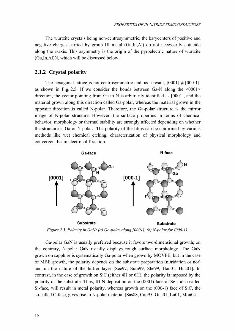
2.1.2 Crystal polarity
The hexagonal lattice is not centrosymmetric and, as a result, [0001] ≠ [000-1], as shown in Fig. 2.5. If we consider the bonds between Ga-N along the <0001> direction, the vector pointing from Ga to N is arbitrarily identified as [0001], and the material grown along this direction called Ga-polar, whereas the material grown in the opposite direction is called N-polar. Therefore, the Ga-polar structure is the mirror image of N-polar structure. However, the surface properties in terms of chemical behavior, morphology or thermal stability are strongly affected depending on whether the structure is Ga or N polar. The polarity of the films can be confirmed by various methods like wet chemical etching, characterization of physical morphology and convergent beam electron diffraction.
Figure 2.5. Polarity in GaN: (a) Ga-polar along [0001], (b) N-polar for [000-1].
Ga-polar GaN is usually preferred because it favors two-dimensional growth; on the contrary, N-polar GaN usually displays rough surface morphology. The GaN grown on sapphire is systematically Ga-polar when grown by MOVPE, but in the case of MBE growth, the polarity depends on the substrate preparation (nitridation or not) and on the nature of the buffer layer [See97, Sum99, She99, Han01, Hua01]. In contrast, in the case of growth on SiC (either 4H or 6H), the polarity is imposed by the polarity of the substrate. Thus, III-N deposition on the (0001) face of SiC, also called Si-face, will result in metal polarity, whereas growth on the (000-1) face of SiC, the so-called C-face, gives rise to N-polar material [Sas88, Cap95, Gua01, Lu01, Mon04].
[0001] [000-1]
INTRODUCTION TO III-NITRIDE SEMICONDUCTORS AND INTERSUBBAND TRANSITIONS
11
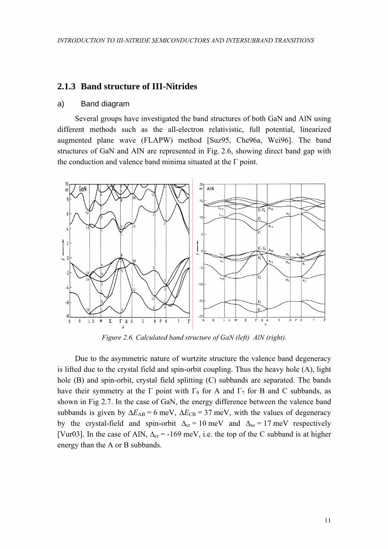
2.1.3 Band structure of III-Nitrides
a) Band diagram
Several groups have investigated the band structures of both GaN and AlN using different methods such as the all-electron relativistic, full potential, linearized augmented plane wave (FLAPW) method [Suz95, Che96a, Wei96]. The band structures of GaN and AlN are represented in Fig. 2.6, showing direct band gap with the conduction and valence band minima situated at the Γ point.
Figure 2.6. Calculated band structure of GaN (left) AlN (right).
Due to the asymmetric nature of wurtzite structure the valence band degeneracy
is lifted due to the crystal field and spin-orbit coupling. Thus the heavy hole (A), light hole (B) and spin-orbit, crystal field splitting (C) subbands are separated. The bands have their symmetry at the Γ point with Γ9 for A and Γ7 for B and C subbands, as shown in Fig 2.7. In the case of GaN, the energy difference between the valence band subbands is given by ∆EAB = 6 meV, ∆ECB = 37 meV, with the values of degeneracy by the crystal-field and spin-orbit ∆cr = 10 meV and ∆so = 17 meV respectively [Vur03]. In the case of AlN, ∆cr = -169 meV, i.e. the top of the C subband is at higher energy than the A or B subbands.

PROPERTIES OF III-NITRIDE SEMICONDUCTORS
12
Figure 2.7. Schematic representation of the valence band splitting in wurtzite GaN.
The band gap of binary compounds like GaN and AlN have been well established long back, but lot of ambiguity surrounded InN until the year 2001. Now a consensus has been reached on a value 50% lesser than previously obtained values of 1.9 eV [Guo94]. Advances in epitaxial growth techniques have allowed fabrication of single crystal InN exhibiting a fundamental gap of ~ 0.62 eV. The band parameters for GaN, AlN and InN have been summed up in Table 2.II. For ternary compounds like AlGaN or InGaN the band gap is approximated by a quadratic equation:
Eg(AB)= x Eg(A) + (1-x) Eg(B) - x(1-x) b (2.2)
where b is the bowing parameter, which accounts for the deviation from a linear interpolation between the two binaries A and B. The bowing parameter has value of 1-1.5 eV [Ste98, Lee99] in the case of AlGaN.
InN GaN AlN Eg(T = 300 K) (eV) 0.66± 0.02 3.39 6.2 Eg(T = 0 K) (eV) 0.62± 0.02 3.48 6.28
ε0 15.3 8.9 8.5 ε∞ 8.4 5.35 4.77
α (meV/K) 0.414 0.909 1.999β (K) 454 830 1429
Table 2.II. Band parameters of InN, GaN and AlN.
A(Γ9)
B(Γ7)
C(Γ7)
Γ6
Γ1 Γ7
Γ8
∆so = 17 meV
Crystal field both Spin-orbit coupling C
B
A
CB
6 meV
∆cr = 10 meV

INTRODUCTION TO III-NITRIDE SEMICONDUCTORS AND INTERSUBBAND TRANSITIONS
13
In semiconductors, the band gap depends upon the temperature mainly due to the lattice expansion and the electron-lattice interaction. The evolution of the band gap with temperature can be represented by the expression below proposed by Varshni et al. [Var67]:
TTTETE+β
α==
2
gg - 0)( )( (2.3)
where α and β are constants calculated taking into account the electron-phonon interaction. There is widespread values reported in the literature. In my calculations, I used the values published in [Vur01] for simulation of GaN and AlN heterostructures (see Table 2.II).
b) Effective masses
Figure 2.8 shows the bands around the Γ point for GaN and AlN. We observe that Γ9 symmetry is heavy along all the k directions, but Γ7 is strongly anisotropic, for instance, light along kx and ky directions and heavy along kz for GaN. It is therefore important to account for such anisotropic effective masses during band engineering design of heterostructures. Table 2.III lists reported values of the average electron and hole effective masses of AlN and GaN materials.
Figure 2.8. Valence band structure of (a) GaN (b) AlN, indicating the anisotropy.
Electron effective mass Hole effective mass GaN 0.2 m0 [Per96, Dre95] 0.3 m0 [Sal95]
2.2 m0 [Im97] 0.54 m0 [Mer96] 0.8 m0 [Pan75] 1 m0 [Vur01]
AlN 0.32 m0 [Vur01, Dre95] 1.41 m0 [Kim97] Table 2.III. Effective masses of wurtzite GaN and AlN.

PROPERTIES OF III-NITRIDE SEMICONDUCTORS
14
c) Band offsets
Heterostructures, with band discontinuities for valence band (VBO) and conduction band (CBO), have dual importance optically and electrically: optically they can be used to form waveguides and electrically to observe quantum phenomena. For the GaN/AlN, InN/GaN and InN/AlN systems, the band offset presents a type I configuration, i.e. in a quantum well, both electrons and holes are confined in the smaller band gap material. Tables 2.IV, 2.V and 2.VI give the theoretical and experimental values of band offsets for different binary compound combinations.
VBO (eV) CBO (eV) Remarks and ref. 0.8 1.8 GaN in-plane lattice [Dan02] 1.3 1.5 SiC in-plane lattice [Dan02] 0.2 - Stained on GaN [Fab97] 0.85 - Strained on AlN [Fab97] 0.87 - Relaxed GaN/AlN[Nad01]
0.7±0.24 2.1 [Mar96] 0.81 - [Su96]
- 1.78 [Hel03] 1.75 [Tch06]
Table 2.IV. GaN/AlN valence band offset (VBO) and conduction band offset (CBO).
VBO (eV) CBO (eV) Ref. 0.5 2.2±0.1 [Chu05]0.48 - [Su96]
1.05±0.2 - [Mar96]- 1.68±0.1 [Kej07]
0.58±0.08 2.22±0.1 [Kin08] 0.85 1.82 [Zah07]0.3 - [Chr97]
Table 2.V. InN/GaN band offsets.
VBO (eV) CBO (eV) Ref. 1.52±0.17 4.0±0.2 [Kin07]
- 3.3 [Tom09]1.81±0.2 - [Mar96]
- 2.45 [Wu06] 1.25 - [Su96]
Table 2.VI. InN/AlN band offsets.

INTRODUCTION TO III-NITRIDE SEMICONDUCTORS AND INTERSUBBAND TRANSITIONS
15
2.1.4 Spontaneous and piezoelectric polarization
a) Material constants
Owing to the polar nature of the cation-N bonds, the Ga-N bond in the (0001) has a non-zero dipole moment. In cubic materials this dipole moment is cancelled with other bonds in the unit cell due to high symmetry in the structure (no spontaneous polarization), but the intrinsic asymmetry in hexagonal wurtzite structure preserves this dipole moment leading to spontaneous polarization in the material, orienting the dipoles along the [0001] direction. Bernardini et al. [Fab01] theoretically calculated the spontaneous polarization in AlxGa1-xN as a function of the Al content x.
Psp = -0.090x – 0.034(1-x) + 0.021x(1-x) [C/m2] (2.4)
The asymmetry can be further enhanced when strained on materials with a lattice mismatch- a source of additional piezoelectric polarization. The importance of understanding the dominance of either spontaneous or piezoelectric polarization must be stressed here because it is different for various material combinations in heterostructures. For example, in the AlGaN/GaN system, the difference in spontaneous polarization is high and its effect is comparable to piezoelectric polarization- or even dominant, as a function of the strain state. In the GaN/InGaN system, the lattice mismatch is larger and the difference is spontaneous polarization is smaller, so that the piezoelectric polarization dominates.
These polarization complexities in III-N can be eliminated by appropriately choosing the growth orientation. The calculations by Takeuchi et al. has helped identify crystallographic directions for which polarization effects are either very small or zero [Tet99]. The results of Takeuchi again point to some of the high symmetry planes of wurtzite GaN at angles 39° and 90° off the (0001) direction. The planes which satisfy these angles are (11-20), (10-10) for 90° and (11-24), (10-12) for 39°. This thesis mostly involves the study of samples grown along polar (0001) orientation except wherever indicated.
The piezoelectric polarization field, Ppz, is related as follows to piezoelectric constants eij and deformation of a crystal εj.
Ppz = ∑eij εj (2.5)
The equation says strain applied to the material changes the dipole moment along the [0001] axis, as a consequence induces macroscopic polarization with magnitude linearly dependent on the polarization tensor of the material. The equation can be written in a different form:
Ppz = ∑dij σj (2.6)
Here Ppz is linearly related to all components of general stress σj and piezoelectric moduli dij. Both the above equations tell the same concept and are related by Hooke’s

PROPERTIES OF III-NITRIDE SEMICONDUCTORS
16
law, which states that, for small stress, the amount of strain is proportional to the magnitude of the applied stress. Therefore,
σi = ∑Cijεj, (2.7)
where Cij is the stiffness or elastic constant tensor. In this thesis we will stick to eij (dkj Cjl) for theory and calculations for the sake of uniformity.
In the case of wurtzite structure, due to the crystal symmetry, the elastic constant tensor contains five independent coefficients, as described below:
( )⎟⎟⎟⎟⎟⎟⎟⎟
⎠
⎞
⎜⎜⎜⎜⎜⎜⎜⎜
⎝
⎛
−
=
121121
44
44
331313
131112
131211
000000000000000
000000000
CCC
CCCCCCCCCC
Cij (2.8)
The value of elastic coefficients measured and calculated by various groups for InN, GaN and AlN are summarized in Table 2.VII.
C11 C12 C13 C33 C44 References
271 124 94 200 46 [Kim96] theory InN
223 115 92 224 48 [Wri97] theory 374 106 70 379 101 [Tak96] exp. 390 145 106 398 105 [Pol97] exp. 365 135 114 381 109 [Yam97] exp. 370 145 110 390 90 [Deg98] exp. 396 144 100 392 91 [Kim96] theory
GaN
367 135 103 405 95 [Wri97] theory 411 149 99 389 125 [McN93] exp. 410 140 100 390 120 [Deg98] exp. 398 140 127 382 96 [Kim96] theory
AlN
396 137 108 373 116 [Wri97] theory Table 2.VII. Experimental and theoretical stiffness constants of InN, GaN and AlN in GPa.
During heteroepitaxy of III-nitrides on the (0001) plane, the in-plane stress is uniform (σx = σy = σ) and there is no stress along the c axis or shear stress. In that particular case (biaxial stress configuration), equation (2.7) gives:
εy = εx ; εz = -2(C13/C33)εx (2.9)
where εz = c-c0/c0, and εx = εy = a-a0/a0, c0 and a0 being the unstrained lattice parameters.

INTRODUCTION TO III-NITRIDE SEMICONDUCTORS AND INTERSUBBAND TRANSITIONS
17
Due to crystal symmetry we have only three non-zero independent constants e33, e31 and e15, so that equation (2.4) can be written as:
⎟⎟⎟⎟⎟⎟⎟⎟
⎠
⎞
⎜⎜⎜⎜⎜⎜⎜⎜
⎝
⎛
εεεεεε
×⎟⎟⎟
⎠
⎞
⎜⎜⎜
⎝
⎛=
6
5
4
3
2
1
333131
15
15
PZ
0000000000000
Peee
ee
r (2.10)
Incorporating equation (2.9) in (2.10), we obtain that for the case of biaxial strain the piezoelectric polarization is a vector along the [0001] axis, whose module is obtained by:
Ppz = 2 εz (e31 – e33 C13/C33) (2.11)
The spontaneous and piezoelectric polarization constants for InN, GaN and AlN are indicated in Table 2.VIII. We observe that the magnitude of piezoelectric constants is ten times higher than GaAs or CdTe compounds, due to the strong ionic character of the III-N bond. In bulk materials, rearrangement of surface charges cancels spatially-uniform polarization-induced electric fields. However, for heterostructures, variation in composition and strain induces internal electric fields in the layers.
e33 (C/m2) e31 (C/m2) PSP (C/m2)InN 0.97 0.57 0.032 GaN 0.73 0.49 0.029 AlN 1.46 0.60 0.081 GaAs 0.12 0.06 - CdTe 0.03 -0.01 -
Table 2.VIII. Spontaneous and piezoelectric coefficients of various semiconductors. Note no spontaneous coefficients for GaAs and CdTe (cubic symmetry materials).
b) Polarization effects in heterostructures
We know that the band gap of GaN is smaller in comparison to AlN, so any abrupt change in material results in abrupt band offset at the semiconductor hetero-interface which must be step-like in normal cases. However, the difference in spontaneous and piezoelectric polarization across the heterointerface affects the band structure to a large extent in III-N, leading to charge depletion or interface charge accumulation. The amount of charges at the interface depends on the strain and material composition.
The difference in polarization across the interface is given by
∆P = ∆(Psp + Ppz) = σpol (2.12)

PROPERTIES OF III-NITRIDE SEMICONDUCTORS
18
The polarization difference results in a fixed charge sheet, σpol, at the heterointerface. Now, let us try and identify the modification in the band diagram introduced by this fixed interface charge. Figure 2.9 shows the sign of the polarization vectors and the resulting σpol for different cases. For instance, in the case of AlN strained on GaN, both the difference in spontaneous and piezoelectric polarization lies in the same direction, leading to positive σpol at the interface and hence to the formation of a two-dimensional electron gas (2DEG) in GaN by rearrangement of free carriers. Conversely, when GaN is compressively strained on an AlN buffer layer, the polarization difference have opposite sense, leading to negative σpol, and hence to a depletion region in the GaN. The corresponding band diagrams are depicted in Fig. 2.10.
Figure 2.9. Polarization directions and sheet carrier density in GaN and AlN for different conditions of strain in: (a) unstrained GaN or AlN or InN (b) tensile strained AlN grown on relaxed GaN buffer (c) Compressive strained GaN on relaxed AlN buffer, (d) Compressive strained InN on relaxed GaN buffer.
(a) (b)
(c) (d)

INTRODUCTION TO III-NITRIDE SEMICONDUCTORS AND INTERSUBBAND TRANSITIONS
19
Figure 2.10. Schematic description of the potential profile at nitride heterojunctions.
In the case of a GaN/AlN superlattice, the material alternation results in a fixed charge at the QW interfaces The electric field in the GaN well, FGaN, and in the AlN barrier layers, FAlN, can be calculated by assuming that the electric field displacement is conserved along the growth direction, which can be visualized in Fig. 2.11: at the circled points we observe that the potential energy at the beginning of the period is equal to the potential energy at the end of the period [Vin99]. The resulting values of the electric field are given by:
GaNAlNAlNGaN
AlNGaN ll
lPF
ε+ε∆= (2.13)
AlNGaNGaNAlN
GaNAlN ll
lPF
ε+ε∆= (2.14)
where lGaN (lAlN) is the QW (barrier) width, εGaN (εAlN) is the GaN (AlN) dielectric constant, and ∆P is the polarization difference at the interfaces.
The electric field in the well sandwitched between two AlN layers causes sawtooth like potential across the active region. In the QW, the internal electric field causes what is know as quantum confined Stark effect (QCSE): the first electron level in the conduction band and the first hole level in the valence band get closer in energy, which implies a red shift of the QW emission energy [Im98]. A complementary effect of QCSE is the spatial separation of electron and hole wavefunctions, which has adverse effect on the interband oscillator strength, displaying large radiative lifetimes.
AlN GaN
[0001]
2DEG
(a) AlNGaN
(b)
GaNInN
(c)

PROPERTIES OF III-NITRIDE SEMICONDUCTORS
20
Figure 2.11 Electron and hole wavefunction separation under the influence of electric field F.
The built-in electric field in III-N heterostructures causes many interesting properties to emerge, which can be either exploited or compensated to our advantage for device design. For instance, the 2DEG formed at the GaN/AlGaN interface can be used to fabricate high electron mobility transistors (HEMTs), with sheet carrier concentration comparable to those obtained by doping the channel. Since the structures are non-intentionally doped, the mobility is not degraded on scattering by the presence of ionized donors which is the case.
2.1.5 Extended defects in GaN
The lack of bulk GaN substrates forces us to perform heteroepitaxy of GaN on substrates like sapphire, Si (111) and SiC. There are different possible paths to relax the misfit-induced strain in the GaN epilayer: the formation of an undulation of the surface that relaxes the strain elastically, crack propagation (tensile strain) or decohesion of the layer (compressive strain), or introduction of misfit dislocations, either through glide of pre-existing threading dislocations or nucleation and expansion of half loops with increase in layer thickness [Mar87]. Plastic relaxation in semiconductors with cubic symmetry, such as silicon and GaAs, usually takes place along the <110> 111 main slip system, either by nucleation of dislocation half loops at the growth surface or by bowing of pre-existing threading dislocations into the heterointerface [Mat74]. However, it is not clear how semiconductors with hexagonal symmetry, such as III nitrides, relax the misfit stress. In the case of nitride heterostructures grown along the [0001] axis, the <11-20> 0002 main slip system
∆EV
∆EC
(0001)
F
AlN GaN AlN
The potential at the beginning and at end is the same

INTRODUCTION TO III-NITRIDE SEMICONDUCTORS AND INTERSUBBAND TRANSITIONS
21
lies parallel to the heterointerfaces, which means that the resolved misfit stress on the main slip plane is zero [Pon97]. Thus, only secondary slip systems that are oblique to the basal plane, such as <11-23> 11-22, can have a resolved misfit stress and may contribute to plastic relaxation.
The dominant extended defects in III-nitride heteroepitaxy are threading dislocations (TDs) [Wu96, Pon97, Nin96] and stacking faults (SFs) [Sta96, Nor98, Pot00, Ver99]. The corresponding dislocations are perfect or partial, with the Burgers vectors b summarized in Table 2.IX. At the interface with the substrate GaN presents a high density of regularly-spaced 60o dislocations (type-B), formed due to large mismatch. These 60° dislocations present at the basal plane have the largest mobility of dislocation glide. These type-B dislocations later tend to bend in the growth direction forming pure edge type a or a+c dislocations. In the c-plane orientation, the main defects are perfect TDs [Nak00], with either edge, screw or mixed character (Burgers vectors 1/3<11-20>, <0001> or 1/3<11-23>, respectively) [Wu96]. Such TDs have their lines in the prismatic 11-20 or 10-10 planes. They form due to the mosaic growth mode [Pon97, Nin96], and appear at the grain boundaries [Pot00b]. They may also be generated during reactions of the numerous basal stacking faults (BSF) [Lor00] that are present in the buffer layers [Pot00]. TDs relax the residual strain that is not entirely compensated by the misfit dislocations at the GaN/sapphire interface [Kwo05]. An important characteristic of the (0001) growth orientation is that the 11-20 and 10-10 lattice planes contain the growth direction [0001] and they constitute slip planes for the TDs. Therefore, as soon as they are formed, such dislocations are able to propagate until the surface of the epitaxial layer.
Dislocations br
Type Character >< 02113/1 A Perfect >< 32113/1 a+c Perfect
>< 0001 C Perfect >< 00113/1 Shockley partial >< 32206/1 Frank-Shockley partial >< 00012/1 Frank partial
Stacking Faults Rr
Type Stacking sequence or plane >< 00113/1 B-I1 ABABCBCB >< 32206/1 B-I2 ABABCACA >< 00012/1 B-E ABABCABAB >< 01112/1 P 0211 >< 32206/1 P 0211
Table 2.IX. Dislocations and stacking faults in hexagonal structure. P: prismatic, B: basal and SS: stacking sequence.

PROPERTIES OF III-NITRIDE SEMICONDUCTORS
22
A BSF is a mistake in the normal ABABABA… hexagonal stacking sequence along the [0001] direction. They are known as intrinsic (I1 and I2) and extrinsic (E). Their stacking sequence and displacement vector ( R
r) are given in Table 2.IX. For
prismatic stacking faults (PSFs), the displacement Rr
takes place out of the basal plane [Dru65, Bla64]. In GaN and AlN, two displacement vectors have been reported to characterize the PSFs in 11-20 planes [Rut99, Nor98, Ver99]. Inside nitride layers grown along the c-axis, SFs are limited close to the interface with the substrate [Nor96].
The above-described structural defects degrade the epilayer electrical and optical properties. For instance, TDs behave as non-radiative recombination centers [Li04] and BSFs and PSFs induce bound photoluminescence transitions around 3.40 eV and 3.2 eV, respectively, which generally predominates over the band-to-band transition in nonpolar or semipolar layers [Lui05].
2.2 Physics of intersubband transitions In this section, I will introduce the physics and basic equations governing the ISB
transitions. A brief discussion of the material properties which influences the device design and operation will be touched upon.
2.2.1 Selection rules
As per the Bloch theorem, the total electron wavefunction ψ(r,t) at the Γ point is the product of Bloch function uv(r), which varies with the materials crystalline periodicity, and the envelope function fn(r), a slowly varying plane wave in comparison to the Bloch function. This means that uv(r) is modulated by the envelope function.
According to the above argument, we can represent the wavefunction in a QW system as:
htiEvnn
nerurftr /− )( )( = ),(ψ (2.15)
where n is the quantum number, and the energy eigenvalue En and the envelope function all depend on the potential of the QW and the externally applied field. In a two-dimensional system like a QW, with discrete energy states, the transition rate Wif from the ground state |ψi> to the final state |ψf> under the influence of an electromagnetic wave with frequency ω is given by the Fermi’s Golden rule.
Wif = (2π/h)|< ψi|H’|ψf>|2 δ(Ef – Ei – hω) (2.16)

INTRODUCTION TO III-NITRIDE SEMICONDUCTORS AND INTERSUBBAND TRANSITIONS
23
where H’= (e/2m*)(A.p + p.A) is the interaction Hamiltonian and m* is the effective mass of the one-band model. A is the vector potential of the electric field E of the plane electromagnetic wave:
E(r,t) = E0 e cos(q.r – ωt) = E0 e (ei(q.r - ωt) + e-i(q.r - ωt))/2 (2.17)
where q is the propagation vector and e the linear polarization vector perpendicular to q. Using E = -∂A/∂t leads to
A(r,t) = E0 e sin(q.r – ω t)/ω = i E0 e ei(q.r-ω t) + c.c (2.18)
Applying the dipole approximation, which states that the wavelength of radiation must be much larger than the characteristic electronic dimension in the material (the periodic potential), satisfied for the ISB transitions, happening within QW of certain width (confined electronic states- envelope). The dipole approximation is thus fulfilled, leading to H’= (e/m*)A.p, and hence
Wif = (2π e2E02/ 4hm*2ω2) |<ψi|e.p|ψf>|2 δ(Ef - Ei –hω) (2.19)
As mentioned before, the wavefunction contains two components: the slowly varying envelope function and superimposed Bloch function. So, the matrix element <ψi|e.p|ψf> can be split as follows.
<ψi|e.p|ψf> = e.<uv|p| uv’><fn|fn’> + e.<uv|uv’><fn|p|fn’> (2.20)
If the initial and final states lie in a different band (v ≠ v’) the overlap integral of the Bloch function <uv|uv’> vanishes and only the first term remains, whose dipole matrix element is built by the Bloch functions. This term represents the interband transitions. When the initial and final states lie in the same band (v = v’), then <uv |p| uv’> vanishes and <uv|uv’> = 1. The second term describes the ISB transitions, whose dipole matrix elements are given by the envelope functions <fn|p|fn’>.
Now, we assume the same Bloch function for both the well and the barrier, and also, since we are dealing with stationary states of the well, the Hamiltonian is considered time-invariant. Therefore, from the wavefunction equation we can separate the envelope function. For the free motion in x and y directions and QW potential V(z) we get:
fnk(r) = A
1 eikr Φn(z) (2.21)
The expression for ISB dipole matrix element for envelope function is
<fnk|e.p|fn’k’> = A1 ∫d3 r e-ikrΦ*n(z) [expx + eypy + ezpz ] eik’r Φ*n’(z) dz (2.22)
Due to the orthogonality of the envelope function, ISB transitions are only allowed between the states having the same wavevector (kn
xy = kn’xy), and for the
transitions between different initial and final states (n ≠ n’) the term ez does vanish.

PHYSICS OF INTERSUBBAND TRANSITIONS
24
The orthogonality condition plays an important role in the interpretation of the quantum system. It simply means that wavefunctions are perpendicular to each other (a.b = 0), the physical interpretation being that if the particle is considered to be ψ1(x), then it cannot be in ψ2(x). The presence of ez in the equation leads to the polarization selection rule, which allows the component of electric field in the z direction to couple to discrete energy levels of the QW. Therefore the dipole matrix element describing the ISB transitions can be written as
<n|pz|n’> = ∫ Φn*(z) pz Φn’* dz (2.23)
Then, the transition rate can be written as
Wif = he
2
2π ez|2 |<n|pz|n’>|2 δ(Ef - Ei –hω) ∆ (2.24)
Where, ∆ is the Kronecker delta to account for momentum requirements. From the above equation it is clear that the ISB transition energy does not depend on the wavevector, as the subbands are parallel to each other. The dipole moments which dictate the oscillatory strength for interband and ISB are different. The interband matrix element is slightly more complex because of the heavy and light hole, which are different along the z and x,y plane. These properties lead to absorption by light holes for TM mode and for light propagating in z direction with polarization along x and y.
On the contrary, ISB transitions happen between the dipoles of the envelope wavefunction increasing with the width of the QW. In a square symmetric potential, the wavefunctions are symmetric and exhibit strong parity selection rule. The system might have even and odd symmetries, but the dipole matrix element becomes zero for wavefunctions with same parity. The oscillatory strength between the energy levels obey the parity selection rule Σfnn’ = 1. In the case of III-N, this rule is relaxed under the presence of strong electric field which forms a triangular asymmetric band structure.
2.2.2 Intersubband linewidth and scattering time
All practical optical transitions have a finite upper state lifetime leading to finite linewidth, normally represented by Lorenzian curve with broadening parameter γ. There are numerous processes in a semiconductor crystal through which carrier scattering can occur: spontaneous emission, scattering by phonons and electron-electron interaction. However, phonon-assisted scattering forms the dominant channel of carrier relaxation when the transition energy is larger than the optical phonon energy.
The scattering can be explained in terms of Fermi’s Golden rule, which states that if an electron or hole in a state i of energy Ei experiences a time-dependent

INTRODUCTION TO III-NITRIDE SEMICONDUCTORS AND INTERSUBBAND TRANSITIONS
25
perturbation H which could scatter (transfer) it into anyone of the final states f of energy Ef, then the lifetime of the carrier in state i is given by
iτ1 =
hπ2 ∑ |<f|Η|i>|2 δ(Ef - Ei) (2.25)
In the case of compound semiconductors with high degree of ionicity in the bonds, mostly the longitudinal optical phonon (LO-phonon) takes part in the scattering process, leading to rapid relaxation of carriers from the excited energy levels. The LO-phonon scattering is dominated by the interaction between the electron and piezoelectric potential created by local deformation [Pri81]. In III-nitrides, Coulomb interaction between the electrons and the longitudinal electric field produced by the LO-phonons, also known as Frohlich interaction, is the main cause of carrier relaxation. Frohlich interaction is strong due to the non-centrosymmetric nature of the crystals, which results in large piezoelectric constants. Pump-probe experiments performed on 2DEG of AlGaN/GaN HEMT structures with very broad absorption spectrum show short relaxation times of 160-180 fs for absorption wavelength at 4 µm, resulting in homogenous line broadening of 50 meV [Wan04, Wan06]. With proper design, this property aids in fabricating high-speed modulators and photodetectors, because of the short time required by the carriers to reach the ground state from the excited state, also know as ‘reset time’. It has been beautifully taken advantage of in the design and demonstration of quantum cascade detectors with phonon ladder [Var08].
Carrier-carrier (electron-electron) interaction is another process by which scattering can occur. Unlike phonons, which introduce a time-dependent perturbation, electron-electron scattering is a time-independent exchange of energy and momentum between the electrons. There are many different processes happening under the general heading of carrier-carrier scattering: ISB process, where at least one or both the carriers change their subband; Auger transition, which causes an electron to relax to a lower subband and a second electron receives the energy released to remain within its original subband; and a third type of process where the number of carriers within a subband remains constant but they interact with electrons of the neighbouring subband.
Electron-electron scattering has spin-dependent character: Pauli’s exclusion principle prohibits electrons with same spin to remain at the same region of space, therefore inhibiting the process of scattering, but electrons still scatter by interaction with electrons of opposite spin, which is known as exchange interaction [Kin98]. So, in an N-level system with 4 carrier states 4N different scattering events are possible. All the observed scattering events conserve energy and momentum. The electron-electron interaction mainly contributes to carrier distribution within the subband, maintaining equilibrium when the transition energy is large. The scattering contribution between subbands is enhanced for low transition energies. Temperature
PHYSICS OF INTERSUBBAND TRANSITIONS
26
and ISB transition energy dependence of scattering events has been deeply investigated by Smet et al. [Sme96].
The contribution of above-described scattering mechanisms (phonon and carrier-carrier scattering) towards line broadening is characterized by time constants T1 and T2, which speak about the relaxation time of carriers from the first excited level to the ground state (ISB) and decoherence between the states participating in the transition (intrasubband), respectively.
2.2.3 Thermal stability
ISB transitions mainly depend on the band offset between two materials. Therefore, ISB transitions are relatively temperature insensitive, but there are few reports of red shift in ISB absorption energy for InAs/AlSb QWs explained by band filling of higher electronic levels and non-parabolicity for high electron wavevectors [Lar03, God94]. In GaN/AlN SLs, there is little or no shift recorded with temperature within the experimental accuracy. In contrast interband transitions show huge variations in bandgap with temperature (emission red shift) because of expansion in the lattice and increased motion of atoms around their mean position or phonon induced broadening.
The ISB scattering time remains largely unaffected with temperature if the LO-phonon energy is higher than kT, since the scattering rate depends on the emission and absorption of phonons i.e., number of phonon available at a given temperature. As in GaN/AlN QWs the LO-phonon energy is ≈ 90 meV >> kT, the possibility of thermally-induced line broadening is very small even at room temperature.
2.2.4 Intersubband optical nonlinearities
An interesting aspect about ISB transitions is the magnitude of the optical transition electric dipole moments, which measure the oscillatory strength between two subbands deciding the linear and nonlinear response of a system. The material system (subbands of the QW) responds in the linear regime when the field generated by the system in response to an external field is proportional to the excitation. Linear optical properties of a system (transmission, absorption, birefringence) have a square dependency on the ISB optical dipole moments.
When the confining potential around the electron is made asymmetric in profile, then the electron orbits tend to distort along the direction of strong potential. The optical response of such an asymmetry is that an external field of frequency ω will generate a harmonic polarized output field of 2ω, known as second harmonic generation (SHG), especially when the inversion symmetry is broken. One can enhance the SHG by playing with various design aspects like separation between the

INTRODUCTION TO III-NITRIDE SEMICONDUCTORS AND INTERSUBBAND TRANSITIONS
27
subbands, asymmetry in the potential etc., keeping in mind not to compromise too much the electron displacement and overlap of the electron wavefunctions.
Resonant SHG has been reported in many material systems such as GaAs/AlGaAs [Bou90], AlInAs/GaInAs, and SiGe/Si (symmetric potential). In comparison to the above material systems, where the asymmetry is forced by band gap engineering, III-N already have the inherent huge electric field originating from the strong spontaneous and piezoelectric polarization, which introduces the desired asymmetry in the quantum system. Double resonant enhancement of SHG has been reported, with a peak conversion at 2 µm wavelength from GaN/AlN QWs [Nev06]. Similarly, there are other nonlinear effects which has been observed in artificially designed quantum heterostructures, like optical rectification, frequency down conversion and third order nonlinearities, mainly DC Kerr effect [Sa’a92], and third harmonic generation [Sir92] and four wave mixing.
Other than above mentioned direct effects of optical nonlinearity, III-nitrides also give an extra edge with the observation of huge carrier-induced refractive index nonlinearity at the ISB absorption wavelength. A change in refractive index can be caused by three major factors, namely carrier injection, band shrinkage, or band filling. Free-carrier absorption has a significant effect on the refractive index n, at NIR wavelengths, as electrons are raised to higher conduction subband levels. The theoretical calculations predict the change in refractive index ∆n by change in carrier concentration ∆N to be of the order of 0.3%/1018 cm-3 [Hui05]. In comparison with InP-based materials, III-nitrides show much less sensitivity towards temperature changes (dn/dT = 10-14 K-1), which demands less stringent control over the operating temperature. The ∆n is symmetric for free carrier absorbing at resonant ISB wavelength, in comparison to index change by band shrinkage and band filling. Thus, III-N heterostructures can be suitably used as phase modulators over a wide spectral range in and around the ISB wavelength for which the structure is designed to absorb. It is interesting to realise phase modulators in the 1.3-1.55 µm range for applications in communications, since such modulators have only been demonstrated for long IR wavelengths [Vag95].

PHYSICS OF INTERSUBBAND TRANSITIONS
28

Chapter 3
Plasma-assisted molecular beam epitaxy of III-nitride materials
The information given in this chapter is intended to serve as an introduction to the plasma-assisted molecular beam epitaxy of III-nitride semiconductors, and as a reference for the understanding of the experimental results described in the following chapters. The main focus of the chapter is on thermodynamics and kinetics of the growth of GaN, AlN and AlGaN. The experimental setups and the substrates used in this work are introduced.
3.1 Epitaxial growth
Epitaxy is defined as the deposition of a monocrystalline film on a monocrystalline substrate, keeping a certain lattice alignment. We speak about heteroepitaxy when the substrate and the epilayer are different materials. The epitaxial growth process depends not only on the thermodynamical properties of the surface but also on the adatom kinetics. [Vil95, Sai96, Mar95, Bar95, Pol00]. The substrate temperature is a key parameter which activates the kinetic processes occurring at the growing surface. Figure 3.1 depicts the different atomistic processes that can take place at the surface during epitaxial growth: adsorption, diffusion, nucleation, incorporation and desorption.
Figure 3.1. Atomistic processes that can occur at the surface during the growth: adsorption, diffusion, cluster nucleation, step-edge growth, and desorption.
Depending on the growth conditions, the behavior of surface processes varies due to the different adatom diffusion length and adatom lifetime. As a function of these parameters, we can characterize the growth modes as illustrated in Fig. 3.2:

EPITAXIAL GROWTH
30
− (a) Multi-layer growth: short diffusion length results in nucleation of multi-layer-thick clusters, ultimately forming a rough surface.
− (b) and (c) Layer-by-layer growth: for increasing diffusion length, the adatoms tend to nucleate in monolayer clusters. The monolayers are completed one by one.
− (d) Step-flow growth: with a longer diffusion length, the adatoms have enough mobility to reach the step edges, which are often energetically favorable incorporation sites.
Figure 3.2. Growth modes as a function of the adatom mobility: (a) multi-layer growth, (b) and (c) layer by layer growth, and (d) step-flow growth.
3.2 Heteroepitaxy
We speak about heteroepitaxy when the substrate and the epilayer are different materials. When considering heteroepitaxy, various growth modes can be observed, depending on the lattice mismatch, surface free energy, and dislocations formation energy:
− Vollmer-Weber: the material tries to keep much of the surface uncovered without wetting. Its the case for materials with large misfit.
− Frank van der Merwe (FvdM): the material tends to decrease surface area effectively wetting the surface or two-dimensional (2D) growth occurs.
− Stranski-Krastanov (SK): The material initially wets the surface, but eventually forms 3D islands over the 2D wetting layer after a critical height.
The three modes of growth in heteroepitaxial systems are shown in Fig. 3.3.
Figure 3.3. Illustration of (a) Volmer-Weber, (b) Frank Van der Merwe and (c) Stranski-Krastanov growth modes.

PLASMA-ASSISTED MOLECULAR BEAM EPITAXY OF III-NITRIDE MATERIALS
31
In the case of wurtzite semiconductors, the elastic energy accumulated per unit of volume is given by:
)()(
)(2)(
221133132211122121211
223
21344
233332
1222
211112
1
ε+εε+εε+ε−+
+ε+ε+ε+ε+ε=
CCCC
CCCU (3.1)
where Cij and εij are the elastic constants and the strain tensor elements, respectively. In the case of biaxial strain of a material grown along the [0001] axis –i.e. ε11 = ε22 = ∆a/a0 ; ε33 = -2C13ε11/C33 ; ε12 = ε13 = ε23 = 0 ; a0 being the in-plane lattice parameter in bulk material–, equation (3.1) is reduced to:
( ) ( )20
20
33
213
1211 //2 aaMaaCC
CCU ∆=∆⎟⎟⎠
⎞⎜⎜⎝
⎛−+= (3.2)
For a layer with a thickness h, the free energy E per unit area defined for FvdM, SK, and SK followed by formation of misfit dislocations can be written as follows [Mar05]:
EFvdM = (1 - d0/d)2 M (∆a/a0)2 h + 2EMD / d + γ (3.3)
ESK = (1 - α) M (∆a/a)2 h + γ + ∆γ (3.4)
ESK+MD = (1 - α) (1 - d0/d)2 M (∆a/a)2 h + 2EMD / d + γ + ∆γ (3.5)
where γ is the films surface energy, α the elastic gain in accommodating films strain through formation of partly relaxed SK islands, ∆γ the surface energy costs for creating facets, d the average distance between misfit dislocations, d0 the distance between misfit dislocations for a fully relaxed layer, and EMD the energy cost per unit length of forming misfit dislocations.
The relaxation will follow the minimum energy path. During the epitaxy of III-nitrides under N-rich conditions, the material being deposited follows a trend such that initially we observe 2D coherent growth followed by SK-mode when the film height exceeds a critical thickness, hSK, and finally leading to coalescence of islands introducing misfit dislocations. In contrast, growth under Ga-rich conditions results in a decrease of the (0001) surface energy that favors FvdM vs. SK growth mode. The ratio (η) of critical thickness for formation of misfit dislocations, hMD, to hSK gives the information on expected type of growth mode, as shown in Fig. 3.4.

HETEROEPITAXY
32
Figure 3.4. Schematic diagram illustrating the growth modes as a function of the layer thickness, h, and the ratio of critical thickness, η = hSK/hMD.
3.3 Plasma-assisted molecular beam epitaxy
There are other methods by which epitaxial growth can be performed, like Metalorganic Vapor Phase Epitaxy (MOVPE), Liquid Phase Epitaxy (LPE), Halide Vapor Phase Epitaxy (HVPE), and Molecular Beam Epitaxy (MBE). MBE is one of the most advanced thin film deposition techniques, invented in the late 1960s at Bell Telephone Laboratories by A. Y. Cho and J. R. Arthur [Cho75]. The MBE technique consists on the evaporation of the desired materials and dopants under ultra-high vacuum (UHV). The sources are generally solids loaded in effusion cells which consist of a crucible surrounded by heating coils (see Fig. 3.5). The sources are evaporated in the form of beams of atoms or molecules at a controlled rate. These atoms deposit and crystallize by reacting with the substrate held at a suitable temperature. The UHV ensures the beam nature of the mass flow towards the substrate, i.e. the mean free path is much longer than the distance between the source cells and the substrate. Under these conditions, the crystal growth is far from thermodynamic equilibrium, and is mostly governed by the kinetics of the surface processes.
Figure 3.5. Description of a standard effusion cell.

PLASMA-ASSISTED MOLECULAR BEAM EPITAXY OF III-NITRIDE MATERIALS
33
RHEED electron gun
Effusion cells
Flux meter
RHEED screen
To substrate heater supplyand variable speed motor
Liquid nitrogen panel
Gate valves
Heating system
Si
Mg
Shutters
Ga (×2)
Al (×2)
In (×2)
Plasmanitrogen cell
Substrate
Sample transfermechanism
Introduction chamber
Transfer chamber
RHEED electron gun
Effusion cells
Flux meter
RHEED screen
To substrate heater supplyand variable speed motor
Liquid nitrogen panel
Gate valves
Heating system
Si
Mg
Shutters
Ga (×2)
Al (×2)
In (×2)
Plasmanitrogen cell
Substrate
Sample transfermechanism
Introduction chamber
RHEED electron gun
Effusion cells
Flux meter
RHEED screen
To substrate heater supplyand variable speed motor
Liquid nitrogen panel
Gate valves
Heating system
RHEED electron gun
Effusion cells
Flux meter
RHEED screen
To substrate heater supplyand variable speed motor
Liquid nitrogen panel
Gate valves
Heating system
Si
Mg
Shutters
Si
Mg
Shutters
Ga (×2)
Al (×2)
In (×2)
Plasmanitrogen cell
Substrate
Ga (×2)
Al (×2)
In (×2)
Plasmanitrogen cell
Substrate
Sample transfermechanism
Introduction chamber
Transfer chamber
RHEED electron gun
Effusion cells
Flux meter
RHEED screen
To substrate heater supplyand variable speed motor
Liquid nitrogen panel
Gate valves
Heating systemHeating system
Si
Mg
Shutters
Si
Mg
Shutters
Ga (×2)
Al (×2)
In (×2)
Plasmanitrogen cell
Substrate
Ga (×2)
Al (×2)
In (×2)
Plasmanitrogen cell
Substrate
Sample transfermechanism
Introduction chamber
Figure 3.6. Schematic of the PAMBE used in this thesis.
In the plasma-assisted MBE (PAMBE) of III-nitrides, active nitrogen is obtained from high-purity (6N5) molecular nitrogen which is cracked by a radiofrequency (RF) plasma source. The MBE used in this work (described in Fig. 3.6) was equipped with an automatic N plasma source HD25 supplied by Oxford Applied Research, described in Fig. 3.7. The high purity N2 is introduced into a pyrolitic boron nitride (PBN) cavity, where the plasma is generated by inductively-coupled RF excitation. The plasma is constantly monitored through an optical feed-back loop.
The low MBE growth temperature typically 600-700oC and the UHV environment result in some advantages for MBE in comparison to other material growth techniques:
• Good control over layer thickness, due to low growth rate (less than one mono-layer per second, and reduced interdiffusion effects.
• Synthesis of a wide range of ternary and quarternary alloys. Even alloys that are barely miscible under thermodynamic equilibrium can be dynamically stabilized by MBE.
• High dopant incorporation. • In situ and real-time characterization by reflection high-energy electron
diffraction (RHEED).
In the particular case of III-Nitride growth, some additional advantages include:

PLASMA-ASSISTED MOLECULAR BEAM EPITAXY
34
• Possibility to change the material polarity, depending on the substrate or buffer layer.
• Activation of Mg-dopant is not required, because of the hydrogen-free growth environment.
Opticaldetector
Window
Gas Inlet
RF matching unit
Water-cooledRF coil
PBN BeamExit Plate
RF shieldPBN discharge tube
Plasma
Opticaldetector
Window
Gas Inlet
RF matching unit
Water-cooledRF coil
PBN BeamExit Plate
RF shieldPBN discharge tube
PlasmaPlasma
Figure 3.7. Photograph and schematic description of the nitrogen plasma cell.
3.4 Reflection high-energy electron diffraction
Since MBE growth takes place in an UHV environment, it is possible to use an electron beam to obtain structural information from the growing surface. Reflection high-energy electron diffraction (RHEED) is a characterization technique that presents the advantage of being in situ and in real time. Electrons are emitted by a hot filament excited by a 1.5 A current and accelerated under high voltage (typically 32 kV in our system). The electron beam strikes the sample at small angle relative to the surface and impinges on a fluorescent screen, so that the image displayed on the screen is the Fourier transform of the lattice interacting with the beam. The schematic description of the measurement is described in Fig. 3.8. From the analysis of the diffraction pattern, we can extract information on the growing surface:
• Determination of the in-plane lattice constant. As illustrated in Fig. 3.9, the interplanar distance du is defined as follows
du = Lλ0/t (3.6)

PLASMA-ASSISTED MOLECULAR BEAM EPITAXY OF III-NITRIDE MATERIALS
35
where L is the distance between the surface normal and the screen, λ0 is the electron wavelength, and t is the distance between two streaks observed in the screen. Therefore du is inversely proportional to t, which has been used to analyze the in-plane strain relaxation during the growth of heterostructures.
Figure 3.8. Schematic description of the RHEED measurement.
Figure 3.9. Schematic description of the procedure to determine the in-plane lattice constant.
• Surface reconstructions. The diffraction patterns can be used to identify
surface reconstructions, which are typical for a particular surface condition. For instance, a stable 2×2 reconstruction is observed for N-rich GaN surface at temperatures below 700oC. The surface consists of one adsorbed N atom per 2×2 supercell.

REFLECTION HIGH-ENERGY ELECTRON DIFFRACTION
36
• Surface morphology. The RHEED pattern is highly sensitive to the surface morphology and crystal quality.
• Determination of the growth rate. The intensity depends on the surface roughness during the layer formation process due to change in density of the atoms. In the case of a flat surface, when the coverage is θ = 0 the RHEED intensity is maximum. Once the coverage increases reaching θ = 0.5, the roughness is maximum and the intensity is at its lowest. At θ = 0.75 the intensity recovers as the space in-between the nucleating sites gets filled and the surface flattens completely at θ = 1, reaching again a maximum RHEED intensity. This sequence is illustrated in Fig. 3.10.
Figure 3.10. Schematic description of the procedure to determine the growth rate from the variation of the RHEED intensity.
3.5 PAMBE of III-nitrides
The PAMBE growth of III-nitrides is performed under constant nitrogen flux which imposes the growth rate. The key parameters which control the crystalline quality and growth kinetics are the substrate temperature, which determines the

PLASMA-ASSISTED MOLECULAR BEAM EPITAXY OF III-NITRIDE MATERIALS
37
adatoms kinetics, and the metallic flux, which modifies the surface energy of the growing layer.
3.5.1 Growth of GaN
The growth of GaN(0001) by PAMBE is extensively discussed in the literature [Ade03b, Neu03, Hey00], and it requires a precise control of the metal-to-nitrogen (III/V) flux ratio. GaN deposition under N-rich conditions proceeds in a layer-by-layer mode that starts with RHEED oscillations that attenuate as the surface roughness increases (see Fig. 3.11). After a few nanometers, the RHEED becomes spotty and the samples are facetted with a high surface roughness. Deposition of 2D GaN layers requires Ga-rich conditions. However, very high Ga flux forms metal droplets on the surface which is detrimental to layer quality. To obtain smooth layers, 2 monolayers (ML) of dynamically-stable Ga are maintained at the growth front, as shown in Fig 3.12. This Ga bilayer allows reduction of the (0001) surface energy by at least 25 meV/A2
, favoring 2D growth. In addition, it was explained by calculations that an efficient diffusion channel is formed underneath this thin metal layer [Nor00].
0 10 20 30 40 50 60 70
Ga/N = 0.78
Ga/N = 0.84
Ga/N = 1.16
Ga/N = 1.0
RH
EED
Inte
nsity
(a.u
.)
Time (s) Figure 3.11 RHEED intensity oscillations and pattern at different III/V ratios.
Figure 3.12. Schematic view of the laterally-contracted Ga bilayer model [Nor00].

PAMBE GROWTH OF III-NITRIDES
38
The Ga excess can be quantified in situ and in real time by RHEED measurements. With this purpose, the GaN surface is exposed to a certain Ga flux, and we study the desorption of Ga under vacuum after stopping the exposure. The RHEED transient duration depends on the amount of Ga which was on the surface [Ade03]. Following the Ga desorption curve after deposition of GaN for 1 min, Adelmann et al. [Ade03b] showed the Ga coverage as a function of impinging Ga flux which is depicted in Fig. 3.13. Four regimes can be distinguished:
A- The quantity of Ga present on the surface is negligible for Φ < 0.3 ML/s.
B- We have the presence of 0 to 1 ML of Ga at the growth front (0.3 ML/s < Φ < 0.5 ML/s).
C- Bilayer of Ga in the growth front ~ 2.4 MLs for flux between 0.5 ML/s and 1 ML/s.
D- The system reaches the Ga accumulation regime, forming metal droplets for flux > 1 ML/s.
Ga Flux (ML/s)
4
6
1.5
A B C D8
10TS = 740°C, ΦN = 0.28 ML/s
Ga
Cov
erag
e(M
L)
1.5
A B C D
T .
1.01.00
2
0.00
0.0 0.50.5
A. N‐Rich Growth
B. Ga excess ≤ 1ML of Ga
C. Ga excess = 2 ML of Ga
D. Accumulation of Ga droplets
Ga Flux (ML/s)
4
6
1.5
A B C D8
10TS = 740°C, ΦN = 0.28 ML/s
Ga
Cov
erag
e(M
L)
1.5
A B C D
T .
1.01.00
2
0.00
0.0 0.50.5
A. N‐Rich Growth
B. Ga excess ≤ 1ML of Ga
C. Ga excess = 2 ML of Ga
D. Accumulation of Ga droplets
Figure 3.13.Ga coverage on top of the GaN(0001) surface as a function of the Ga flux.
The evolution of the above-described four regimes is represented in Fig. 3.14 as a function of the substrate temperature. It is observed that the demand for Ga flux to attain the bilayer conditions increases with the substrate temperature, Ts. The morphology changes from rough texture for N-rich conditions to smooth atomic-step surfaces for Ga-rich growth in the Ga bilayer regime.
The SL structures are usually grown placing ourselves just before the accumulation condition. By choosing this condition the nucleation of V-pits formed due to strain fluctuations, is effectively avoided in the GaN/AlN superlattices (SLs) [Her04].

PLASMA-ASSISTED MOLECULAR BEAM EPITAXY OF III-NITRIDE MATERIALS
39
690 700 710 720 730 740 7500.1
1
<1 ML
2 ML
Stoichiometry
N-Rich Growth
0.3
Ga Accumulation
G
a Fl
ux (M
L/s)
Substrate Temperature (°C)
400 nm
400 nm
400 nm
Figure 3.14. Ga coverage regimes as a function of both substrate temperature and impinging Ga flux.
3.5.2 Growth of AlN
Two important features of AlN growth which must be remembered are: • Growth of AlN does not involve desorption kinetics like GaN because Al
desorbs at temperatures > 800°C. • N has a strong affinity for Al in comparison to Ga, which results in
preferential Al incorporation in presence of Ga [Ili02, Mon03].
In the case of AlN, 2D growth also requires metal-rich conditions, which can be obtained by using an Al/N ratio larger than unity. Since Al does not desorb from the surface at the standard growth temperature for GaN, to eliminate the Al excess at the surface it is necessary to perform periodic growth interruptions under nitrogen. Therefore, to identify suitable growth condition for AlN, we deposit 20 min of AlN with excess Al at Ga desorption temperatures. The excess Al on the surface is observed as extra line or shadow in the RHEED pattern taken along the <11-20> azimuth shown in Fig. 3.15 – this line is the evidence of the reduced lattice constant of metal Al. Next, the surface is exposed to N to consume excess Al. By noting the time required to consume excess Al we can calculate the III/N ratio. This data can be used to play with the Al cell temperature to attain the required stoichiometric growth condition.

PAMBE GROWTH OF III-NITRIDES
40
Figure 3.15. (a) RHEED image of an Al-rich AlN surface (azimuth <11-20>). (b) Intensity profile along the <11-20> direction. The extra streaks due to the Al excss are indicated by the arrows.
However, introducing growth interruptions during the growth of SLs results in degradation of their optical properties [Kan08]. An alternative consists in growing AlN at the stoichiometry and use an additional Ga flux as the surfactant, to improve the mobility of the adatoms at the growing surface. Since the Al–N binding energy is much higher than the Ga–N binding energy, Ga segregates on the surface and is not incorporated into the AlN layer.
3.5.3 Growth of AlGaN
The growth of AlGaN poses some additional difficulties, due to the difference in Ga-N and Al-N binding energy and the different mobility of Ga and Al adatoms on the growing surface. The stronger Al-N bond allows reaction between them irrespective of presence of species like Ga or In in the surroundings [lli02, Mon03]. Therefore, as a first step, the Al flux required to be incorporated in the AlGaN is fixed to a percentage of the N flux corresponding to the targeted Al mole fraction. Then, Ga is used in excess, to obtain a surfactant effect that favors 2D growth. This procedure works for low Al content material valid upto Al < 40%.
For Al contents above 40%, it is necessary to decrease TS to maintain 2D growth, and In can be used as a surfactant to stabilize the surface [Mon03]. Decreasing Ts promotes a balance of diffusion barrier between Al, Ga and N, and enhances the sticking coefficient of In to the surface, which allows modification of surface free energy and kinetics.
3.6 Substrates
Almost all the III-V compounds and Si use bulk materials as the base for homoepitaxial growth. III-N materials are not lucky to have such a situation, as bulk GaN is difficult to form due to high melting temperature and N vapor pressure requirements. Several substrates can be thought as possible choices for heteroepitaxial

PLASMA-ASSISTED MOLECULAR BEAM EPITAXY OF III-NITRIDE MATERIALS
41
growth of GaN, like Sapphire, Si(111), SiC and most recently diamond. A wise choice of substrate for heteroepitaxy should be made by considering lattice constant, thermal expansion coefficient, and requirement of crystal orientation, defect density, purity and surface morphology. Even chemical and electrical properties determine the suitability of substrate for epitaxy from the point of view of device fabrication.
3.6.1 Sapphire-based substrates
Sapphire is the most widely used substrate for GaN heteroepitaxy inspite of the large lattice mismatch of about 30%. Different orientations of sapphire can be used to obtain the various crystallographic directions in GaN. The most common orientation used for GaN is the c-plane sapphire. GaN and AlN grow on sapphire in c-plane orientation, but with in-plane rotation of 30° with respect to sapphire (0001), this rotation reduces the lattice mismatch to 13.9%. The detrimental effects of performing heteroepitaxy on a foreign substrate with huge lattice mismatch can be reduced by sophisticated processing steps like surface treatment followed by nitridation and low temperature buffer layers.
The choice of sapphire-based substrate is important in two senses: technologically the sapphire transparency for ISB devices operating in NIR region is essential, and secondly low dislocation density. The templates used for the experiments are as follows:
− GaN-on-sapphire templates supplied by LUMILOG. The template consists of ~ 10-µm-thick (0001)-oriented GaN with very low dislocation density (~ 108 cm-2).
− AlN-on-sapphire templates procured from DOWA consists of 1.0±0.3 µm thick (0001)-oriented AlN. The FWHM of X-ray ω-scan rocking curve is <100 arcsec for the (0002) reflection, and the dislocation density is ~ 109 cm-2.
Atomic force microscopy (AFM) images of the substrate surfaces are presented in Fig. 3.16.
Figure 3.16. AFM images of (a) the GaN-on-sapphire and (b) the AlN-on-sapphire templates used in this work.

SUBSTRATES
42
3.6.2 Si(111)-based substrates
Silicon is the most widely used semiconductor for applications in electronic industry. Silicon substrates provide many incentives when used as substrates to grow GaN templates: low price of the wafers, large scale production, and good thermal stability under GaN growth conditions. However, greater thermal expansion of GaN as compared to Si (5.6 × 10⁻⁶ K-1 versus 2.6 × 10⁻⁶ K-1) induces a tensile strain on GaN, favoring the formation of cracks in the template during the cooling down process. Moreover, the defect density of GaN-on-Si templates is significantly higher than on sapphire or SiC. The high dislocation densities are attributed to large 23.4% lattice mismatch between AlN and Si thus; reduction of dislocation density holds the key for GaN based devices on Si. Now, various pre-growth surface treatment processes and low temperature buffer layers have shown some improvement in quality of the layers. Techniques such as modified buffer layers with superlattices can be used to filter out the dislocations. Several companies like Picogiga, DOWA and IMEC have managed to produce crack-free GaN-on-Si (111).
The chapter 6 on AlGaN/GaN SLs for mid-infrared (MIR) optoelectronics, particularly deals with active regions grown on GaN-on-Si(111) templates, which is advantageous to overcome sapphire absorption in the MIR without compromising the optical quality in comparison to structures grown on GaN-on-sapphire template. This GaN-on-Si(111) consists of a commercial high electron mobility transistor (HEMT) structure described in Fig. 3.17, grown by MOVPE on floating-zone Si(111). The resistivity of the Si substrate is >6000 Ωcm, the average x-ray rocking curve is ~ 925 arcsec for the (0002) reflection and ~ 1662 arcsec for the (10-12) reflection. The bowing of the 4” wafer was measured to be -24.9 µm. An AFM image of the substrate surface is shown in Fig. 3.18.
GaN 2.5 nm
Al0.27Ga0.73N 18 nm
GaN 0.8 µm
Buffer 1.8 µm
Si(111)
Figure 3.17. Schematic description of the GaN-on-Si(111) templates used in this work.
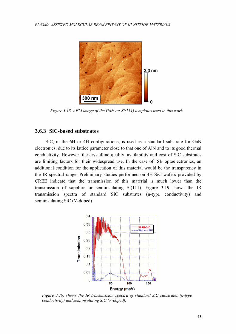
PLASMA-ASSISTED MOLECULAR BEAM EPITAXY OF III-NITRIDE MATERIALS
43
Figure 3.18. AFM image of the GaN-on-Si(111) templates used in this work.
3.6.3 SiC-based substrates
SiC, in the 6H or 4H configurations, is used as a standard substrate for GaN electronics, due to its lattice parameter close to that one of AlN and to its good thermal conductivity. However, the crystalline quality, availability and cost of SiC substrates are limiting factors for their widespread use. In the case of ISB optoelectronics, an additional condition for the application of this material would be the transparency in the IR spectral range. Preliminary studies performed on 4H-SiC wafers provided by CREE indicate that the transmission of this material is much lower than the transmission of sapphire or semiinsulating Si(111). Figure 3.19 shows the IR transmission spectra of standard SiC substrates (n-type conductivity) and semiinsulating SiC (V-doped).
Figure 3.19. shows the IR transmission spectra of standard SiC substrates (n-type conductivity) and semiinsulating SiC (V-doped).

SUBSTRATES
44

Chapter 4
GaN/AlN quantum wells
The chapter begins by explaining the simulation and design aspects of GaN/AlN superlattices (SLs) for intersubband (ISB) absorption, mainly at 1.55 µm. Then, I describe the epitaxial growth where, keeping in line with the previously established growth methods, the essential guidelines to grow structures with minimum relaxation will be presented. The strain relaxation process in the SLs is analyzed through techniques such as reflection high-energy electron diffraction, high-resolution transmission electron microscopy, high-resolution X-ray diffraction and medium energy ion scattering experiments. The effect of relaxation on the ISB absorption wavelength is analyzed. Finally, I discuss the effects of the polarization-induced internal electric field on the ISB absorption, in particular the polarization-induced doping as a function of the cap layer and the effect of polarization in the ISB transition energy by comparison of polar and semipolar structures.
4.1 Introduction
The main reason for rapid research and development of sophisticated optoelectronic devices operating in the near infrared (NIR), and especially in the 1.3-1.55 µm spectral region, is targeted towards applications in telecommunications, where conventional interband devices are reaching their intrinsic speed limits. The requirement for devices with high frequency response which do not suffer from parasitic capacitance due to space charge effects was sensed. Although there are many possible candidates for ISB transitions at short wavelengths, like InGaAs/AlAsSb [Gop02], GaInNAs/AlAs [Ma07], or (CdS/ZnSe)/BeTe [Aki05], III-N outperform these materials in terms of speed. The advantage lays in the strong electron-LO phonon interaction in these highly-ionic nitrides, which results in extremely short intersubband (ISB) absorption recovery times of ~ 150-400 fs, and ultimately paves the way for devices operating in 0.1-1 Terabit per second bit-rate regime [Iiz00]. III-Ns also form excellent candidates for ISB unipolar lasers because scattering to remote lateral valleys is almost ruled out as these valleys lie very high in energy (>2 eV above the Г valley). However, reaching NIR wavelengths requires extremely narrow nitride quantum wells (QWs) because of the large GaN effective mass. This geometrical exigency sets a challenge for high-temperature growth methods like metalorganic vapor phase epitaxy (MOVPE), but can be achieved by low-temperature growth techniques like molecular beam epitaxy (MBE), which offers greater control over the interface formation process.

INTRODUCTION
46
ISB NIR transitions have been observed in QWs of GaN/AlGaN and GaN/AlInN at room temperature [Gma00, Iiz02, Hel03, Tch06, Nic05] with the possibility of extending the wavelength even up to 1 µm [Kis02] due to the large GaN/AlN band offset of ~ 1.75 eV [Tch06]. Since these preliminary results, the understanding of the material and technology has allowed significant progress in the fabrication of device prototypes. There has been an important research effort in saturable absorbers for ultrafast all-optical switching with switching energy as low as 38 pJ for extinction ratio larger than 10 dB [Li07, Hof03]. These switches might find immediate application in optical time division multiplexing systems. QW-based photodetectors with 3 GHz operation bandwidth [Hof06, Gio07] in the photovoltage mode have been demonstrated, and their performance has been justified by the process of optical rectification [Ros90]. Also photoconductive QW photodetectors have been reported, although exhibit low sensitivity, caused by large leakage currents in the presence of high threading dislocation densities [Hof07]. Photodetector designs based on a cascade structure have been proposed [Var08] with responsivity as large as 10 mA/W at 1.7 µm wavelength and bandwidth in excess of 10 GHz [Var08b]. On the other hand, the first quantum dot infrared photodetector working at 1.41 µm with room temperature peak responsivity of 8 mA/W has been demonstrated [Var06]. Electro-optical modulators at NIR wavelengths have also been developed based on two concepts: charge transfer between a two-dimensional electron gas (2DEG) and the active superlattice [Bau06] or electron tunneling between two coupled QWs [Nev07, Khe08]. High frequency modulation up to 10 GHz has been realized, but this technology provides lot of room for performance enhancement by reducing the mesa size to increase the modulation bandwidth and incorporating the active region into a waveguide providing larger modulation depth. Finally, the observation of room temperature light emission from ISB transitions within QWs [Nev06, Nev08, Dri09] and QDs [Jul07] of GaN/AlN provides a ray of hope for fabrication of devices such as quantum cascade lasers (QCLs).
4.2 Calculation of the electronic structure
The reliability of modeling of the electronic structure of III-nitrides is limited because of the uncertainty in physical parameters, the high density of crystalline defects, which is hard to take into account, and the high piezoelectric constants, which make the band structure very dependent on the strain state of the sample. Indeed, the modeling of quantum confinement in nitride QWs must go beyond the flat-band approximation and account for the polarization-induced internal electric field in the QW and in the barriers. Internal electric fields of the order of 5-10 MV/cm are observed in response to the large magnitude of fixed charge density at the GaN/AlN interfaces, which have a significant effect on the electronic structure and optical

GaN/AlN QUANTUM WELLS
47
properties. In addition, strain relaxation modifies polarization difference at the interface and the material bandgap, inducing a shift of the confined electronic levels.
In this work, I used the Nextnano3 solver [Nex], created at Walter Schottky Institute in Munich. With this software, it is possible to calculate not only the electronic configuration of common c-plane III-nitrides but also other semipolar or nonpolar orientations, by indicating the growth axis. The strong advantages of the Nextnano3 solver are that the material parameters are fully accessible and the simulations take into account the spontaneous and piezoelectric polarization coefficients, together with the strain state. To calculate the electronic structure, several models are implemented in the software, namely the effective mass model, the k.p model, and the tight-binding approximation. Each model has its own advantages and disadvantages:
− The effective mass approximation is fast and not demanding in terms of calculation capacity, but it does not incorporate features like the non-parabolicity.
− The k.p theory model, where k represents the wavevector of the Bloch wave and p is the momentum, overcomes the crude assumption of parabolic band structure usually considered for convenience at the bottom of the conduction band and top of the valence band. The model not only allows calculation of energy at k = 0 but also at other wavevectors, by considering values away from k = 0 to be perturbations. Thus, corrections for non-parabolicity can be implemented for wavevectors kz > 0.15 Å-1, i.e. for energies higher than 300 meV from the conduction band minimum.
− Finally, the tight-binding model is well suited for simulating three-dimensional nanostructures, because it follows an approach where band structure is calculated starting from the energy levels of an atom, followed by attaching more atoms to form a crystal. However, it is very demanding in terms of calculation time, so that it is not recommended for structures with one-dimensional symmetry.
For the calculation of the electronic structure of nitride ISB devices, the incorporation of non-parabolicity corrections is critical, due to the huge separation between the electronic levels in the QWs. The effect of non-parabolicity is to reduce the energy level of the excited state and the magnitude of this reduction can be almost 25% in comparison to parabolic cases [Tch06]. Therefore, the simulations presented in this work were performed using the 8 band k.p Schrödinger-Poisson equation solver. In principle, these calculations do not consider many body effects like exchange interaction and depolarization shift, which have significant influence on energy of the ground state at high electron concentrations, and become particularly relevant for transitions in the mid-infrared (MIR) and far-infrared (FIR) spectral regions.

CALCULATION OF THE ELECTRONIC STRUCTURE
48
Considering the above deliberations, it is imperative to choose the right model and the adequate material parameters to obtain the best fit with the experimental observations. Table 4.I provides the list of material constants which I have used to perform the simulations. To calculate the confined electronic levels, I performed the simulation along the growth direction i.e. [0001], with the crystallographic off-axis directed along [10-10]. In general, the calculations assume the lattice at room temperature (T = 300 K) and the structure strained on either GaN or AlN.
Parameters GaN AlN Refs.
Lattice constants [nm] a c
0.318920.51850
0.31120.4982
[Vur03]
Spontaneous polarization [Cm-2] -0.029 -0.081 [Ber97] Piezoelectric constants [Cm-2]
e13 e33
-0.49 0.73
-0.60 1.46
[Ber97]
Elastic constants [GPa] C11 C12 C13 C33
390 145 106 398
396 140 108 373
[Pol96, Wri97]
Dielectric constant 10 8.5 [Par00] Luttinger parameters
A1 A2 A3 A4 A5 A6 A7
//PE [eV] ⊥PE [eV]
-5.947 -0.528 5.414 -2.512 -2.510 -3.202
0 14(*) 14(*)
-3.991-0.3113.671 -1.147-1.329-1.952
0 17.3 16.3
[Rin08]
Deformation potentials [eV] ac1 ac2
D1
D2
D3
D4
D5
D6
-4.6 -4.6 -1.70 6.30 8.00 -4.00 -4.00 -5.66
-4.5 -4.5 -2.89 4.89 7.78 -3.89 -3.34 -3.94
[Par00]
Band offset [eV] 1.8 [Tch06]
Table 4.I. Material parameters used in the theoretical calculations. Data indicated with (*) were corrected to achieve a good fit with the experimental results.
The results of the simulation of a superlattice (SL) of 4 ML and 6 ML thick GaN QWs with 3 nm thick AlN barriers strained on AlN are depicted in Figure 4.1, where the polarization-induced sawtooth potential profile and the shift of the electron wave function along [0001] and the hole wave function towards [000-1] can be observed.

GaN/AlN QUANTUM WELLS
49
Figure 4.1. Band diagram of GaN/AlN QWs in a superlattice with 3-nm-thick AlN barriers and (a) 4 ML thick or (b) 8 ML thick GaN QWs.
Figure 4.2. Band diagram of a GaN/AlN QWs in a SL with 3 nm thick AlN barriers and 1.5 nm thick GaN QWs. The black (gray) lines describe the structure fully strained on AlN (GaN).
The effect of strain on the electronic levels is illustrated in Fig. 4.2, where I compare simulations of a GaN/AlN (6 ML / 3 nm) QW SL strained on AlN (black) and strained on GaN (gray). The variation of the strain state has two main effects on the band diagram:
− Variation of the band gap: the change in the conduction band minimum at the Г point can be parametrized by a linear relation:
∆Ec = ∑ dij εij (4.1)
where dij is the deformation potential. Since the hexagonal crystals exhibit less symmetry than cubic, it is reflected in different deformation potential constants for various directions. In wurtzite structures, we consider two independent deformation potentials d11 = d22 = ac1 and d33 = ac2:
∆Ec = ac1 (ε11 + ε22) + ac2 ε33 (4.2)

CALCULATION OF THE ELECTRONIC STRUCTURE
50
The values of ac1 and ac2 used in the simulations are summarized in Table 4.I. In the case of biaxial strain, equation (4.2) becomes:
∆Ec = 2(ac1 – ac2 C13/C33) ε11 (4.3)
In addition, six deformation potential constants Di arise from a full treatment of the effect of strain on the six-band valence-band structure [Bir74]. These Di are tabulated for each nitride material in Table 4.I.
The variation of the GaN A, B and C exciton energies as a function of strain is presented in Fig. 4.3, where compressive strain widens and tensile strain reduces the overall band gap. This shift of the bands under strain has strong influence on interband transitions in quantum wells.
Figure 4.3. Evolution of the energy of the excitonic lines in undoped GaN depending on the strain state along [0001] axis, assuming biaxial strain [Shi97].
− Variation of the piezoelectric polarization: the piezoelectric constants are larger for the AlN barrier than for the GaN quantum well, which implies an enhancement of piezoelectric polarization for structures that are tensile strained on GaN [Kan09].
A detailed description of the evolution of the interband transition e1-h1 as well as the ISB transitions e2-e1 and e3-e1 with the QW thickness and strain state is presented in Figure 4.4. The experimental results represented by triangles show a good fit with the theoretical calculations performed using the above-described material parameters. We observe a significant shift of the interband transition with strain due to the modification of the GaN band gap, where the error bars indicate the FWHM of the spectra due to the presence of dislocations and interface roughness. This effect is

GaN/AlN QUANTUM WELLS
51
smaller in ISB transitions, which are determined by the conduction band offset instead of the band gap. Therefore, the difference in the e2-e1 transition energy for structures strained on GaN or AlN is mostly due to the difference in piezoelectric polarization. This ISB shift cannot be neglected, since the difference in transition is large enough to be detected in samples experimentally.
1.5 2.0 2.5 3.0
2.5
3.0
3.5
4.0
e 1-h1 E
nerg
y (e
V)
QW Thickness (nm)
Strained on GaN Strained on AlN
T = 7 K
(a)
1.0 1.5 2.0 2.50.4
0.6
0.8
1.0
1.2
1.4
1.6 (b)
e1-e3
e1-e2
Ener
gy (e
V)
QW Thickness (nm)
Strained on GaN Strained on AlN
T = 300 K
Figure 4.4. Evolution of interband and ISB transition energy as a function of the QW thickness in GaN/AlN SLs with 3 nm AlN barriers. (a) Comparison of e1-h1 energy for SLs strained on GaN and AlN. (b) Variation of the e1-e2 and e1-e3 ISB transition energy as a function of the QW thickness. Triangles indicate experimental data and solid and dashed lines correspond to theoretical calculations assuming the structure fully strained on AlN and on GaN, respectively.
From the variation of transition energy represented in Figure 4.4(b), we can deduce that ~ 6 ML QW width is required for ISB absorption at 1.55 µm (= 0.8 eV) wavelength using 3 nm of AlN barrier. Realizing the above stringent requirement of very short period GaN/AlN SLs presents several growth challenges to obtain uniform, sharp and strained defect-free interfaces. To reach shorter wavelengths we can choose other well/barrier widths (i.e. 1 nm GaN / 2 nm AlN), but designs with very small well width are more sensitive to monolayer fluctuations, resulting in multiple peaks at the ISB resonance. On the other hand, larger AlN barriers cause difficulties in carrier conduction through the structure.
4.3 Growth conditions for GaN/AlN QWs All the samples described in this thesis were synthesized by plasma-assisted
molecular-beam epitaxy (PAMBE). The SL growth conditions were optimized taking as a base the know-how on the growth of GaN and AlN layers (see chapter 3), and determining the growth conditions that minimize the strain relaxation. We have first addressed the growth of the binary compounds GaN and AlN, and the conclusions have been applied to the heterostructures. During growth, the strain relaxation was analyzed in situ using reflection high-energy electron diffraction (RHEED), measuring

GROWTH CONDITIONS FOR GaN/AlN QWS
52
the distance between the (10) and (-10) streaks in the (11-20) azimuth, which is inversely proportional to the in-plane lattice constant. In addition to measuring the relaxation, we can also monitor the evolution in surface morphology which could be later compared with the relaxation events.
The growth of GaN(0001) by PAMBE is extensively discussed in the literature [Ade03, Neu03, Fee02, Hey00, Nor00], and it requires a precise control of the metal-to-nitrogen III/V flux ratio. Since the materials we deal with are group III-N, which are strongly bonded and exhibit high melting temperatures especially AlN, low temperature growth methods like MBE usually produce rough morphologies for wide range of growth conditions. To our advantage, it was identified that a process called adlayer enhanced lateral diffusion (AELD), enables growth of materials with high melting point at moderate temperatures [Neu03]. It was explained by calculations that an efficient diffusion channel is formed underneath a thin metal layer on top of the growing surface. For AELD to occur, this metal adlayer should consist of at least two monolayers of metal on the surface and diffusion of adatoms to the subsurface must be possible, which is the case when the atomic radius of adsorbates is significantly smaller than the host adatoms.
In agreement with this description, deposition of two-dimensional (2D) GaN layers is possible under both In-rich and Ga-rich conditions, and hence growth optimization translates into the determination of the adequate metal excess and growth temperature. In this thesis, the GaN layers were systematically grown under Ga-rich conditions. At a substrate temperature higher than 700°C and for a certain range of Ga fluxes, the Ga excess remains on the growing surface in a situation of dynamical equilibrium, i.e. the Ga coverage is independent of the Ga exposure time. It is possible to stabilize a Ga amount from below 1 ML up to 2.5 ML. However, smooth surfaces can only be achieved with a Ga coverage of 2.5±0.1 ML, when the Ga excess arranges into a so-called “laterally contracted Ga bilayers,” which consists of two Ga layers adsorbed on the Ga-terminated (0001) GaN surface. These growth conditions delay GaN lattice relaxation to the point that residual in-plane strain in the range of 0.2-0.3% is still measured in 1 µm-thick GaN layers [Bel03].
The surface morphology of GaN/AlN superlattices strongly depends on Ga/N ratio, even within the Ga bilayer growth window [Kan08]. The strain fluctuations induced by alternating GaN and AlN layers favor the formation of V-shaped pits [Nak02, Her04]. The V-shaped pits are a favorable relaxation channel in GaN-based materials because of the kinetic hindrance offered to the glide of threading dislocations, which is overcome by formation of the pits with 10-11 facets [Son05, Nor99]- a consequence of the difference in surface energy between the (0001) and 10-11 planes. In the case of the GaN/AlN system, these defects are minimized by increasing the Ga flux, so that growth is performed at the limit of Ga accumulation on

GaN/AlN QUANTUM WELLS
53
the surface [Kan08]. This is explained by the strong decrease of the (0001) surface energy with increasing III/V ratio [Ros06], which favors 2D growth.
In the case of AlN, 2D growth also requires metal-rich conditions, which can be obtained by using an Al/N ratio larger than unity. However, it must be remembered that Al does not desorb from the surface at the standard growth temperature for GaN. Therefore, to eliminate the Al excess at the surface, it is necessary to perform periodic growth interruptions under nitrogen. However, introducing growth interruptions results in degradation of the optical properties of the SLs [Kan08]. Drawing motivation from the above theoretical discussion on the AELD method, we have modified the growth process for AlN using Ga as a surfactant, with the Al flux corresponding to the Al/N stoichiometry and an additional Ga flux to stabilize the surface. Since the Al–N binding energy is much higher than the Ga–N binding energy, Ga segregates on the surface and is not incorporated into the AlN layer [Ili02].
We have performed systematic experiments to identify the AlN growth conditions which induce minimum relaxation when growing on relaxed GaN. AlN was deposited on GaN under different III-V ratios for about ~ 180 s at a growth rate of 0.3 ML/s. The experiments were performed at a substrate temperature of 720°C, to remain compatible with the GaN growth. We have studied different deposition conditions:
1. Al/N = 1 at stoichiometry 2. Al/N = 1 with an additional Ga flux to stabilize the surface, corresponding to
the formation of 2 ML of Ga excess on GaN 3. Al/N = 0.97 with an additional Ga flux
0 40 80 120 160 2003.160
3.165
3.170
3.175
3.180
3.185
3.190
a La
ttice
Con
stan
t
Time (s)
Al/N = 1 Al/N = 1 + Ga excess Al/N = 0.97 + Ga excess
Figure 4.5. Variation of in-plane lattice parameter of AlN grown on GaN, measured in situ by RHEED for various AlN growth conditions. The Al and N shutters open at time t = 0.
Figure 4.5 presents the evolution of the in-plane lattice parameter during the growth of AlN on GaN. In all cases, we can discriminate two stages of the growth:

GROWTH CONDITIONS FOR GaN/AlN QWS
54
1) In a first stage, the lattice parameter drops sharply during the growth of ~1 nm and partially recovers at about 10-35 s, depending on growth conditions. Simultaneously, the RHEED pattern turns bright and slightly irregular. These observations point to an initial three-dimensional elastic (i.e. reversible) relaxation.
2) The lattice constant stabilizes at a certain value. The difference between the initial (t = 0) and final lattice parameters is the measure of plastic relaxation, i.e. the irreversible strain release by misfit dislocations or generation of cracks.
To understand this result, we must keep in mind that misfit stress can relax either by roughening or by dislocation formation. The critical thickness and relaxation path depend on the accumulated elastic energy, the surface free energy, and the energy required for generation of a dislocation, as described in section 3.2. In III-nitrides, the absence of favorable gliding planes results in high misfit dislocation formation energy, which privileges roughening as relaxation path. As the system is not in a stable state when very thin layers of AlN are strained on GaN, the system eventually drifts towards stable state by initially relaxing elastically-increasing the surface free energy which helps attain the energy required to relax plastically later on through channels like dislocations. If the growth continues after the initial roughening, the accumulated elastic energy can ultimately reach the threshold of plastic relaxation via structural defects.
From Fig. 4.5 we can conclude that the magnitude of elastic and plastic components varies as a function of growth conditions. By choosing the growth parameters which display minimum plastic relaxation we fix the most suitable conditions to grow the SLs (i.e., Al/N=1 + Ga excess).
The reduced relaxation under high III/V ratios can be explained by the decrease of the (0001) surface free energy [Nor00] which results in an attenuation of the elastic relaxation component. Roughening reduces the dislocation formation threshold, since the presence of free surfaces intercepting the heterointerfaces can favor dislocation slip on the basal plane [Mei07]. Therefore, the attenuation of roughening by increasing the III/V ratio might bring a delay of the plastic relaxation as a secondary effect. On the other hand, the surface mobility of the adsorbed species increases with the III/V ratio [Zyw98], which reduces the probability of forming dynamically-induced structural defects, such as basal stacking faults (BSFs). This is relevant for the growth of AlN on GaN, since the mobility of the adatoms of AlN is particularly low at the growth temperatures under study (T = 720°C), required to prevent GaN/AlN interface degradation [Gog04].

GaN/AlN QUANTUM WELLS
55
4.4 Strain relaxation in GaN/AlN superlattices
Using the growth conditions described in section 4.3, we have studied the strain relaxation during the growth of GaN/AlN (1.5 nm / 3nm) short-period SLs deposited either on GaN-on-sapphire or on AlN-on-sapphire templates. The strain relaxation has been first measured in situ by RHEED, and then the results were compared with ex-situ structural characterization techniques like X-ray diffraction (XRD), transmission electron microscopy (TEM), and medium energy ion scattering (MEIS), to gain a complete picture of the relaxation mechanisms and defect structure.
It is important to outline that the GaN/AlN SLs studied in this section do not present cracks. Crack-free growth of GaN/AlN structures on GaN templates is possible by the above-described growth technique which uses a Ga excess even during AlN growth. Similar structures with AlN barriers grown using Al excess and followed by growth interruptions under N display cracks.
The variation of in-plane lattice constant during growth was measured in real time by RHEED. It must be remembered that it is difficult to quantify the exact lattice constant of the materials by RHEED due to inherent limitations like the differing distance between the screen and the spot where the electron beam reflects from the substrate surface and the angle of the incident beam. Thus, from the measurement of distance between the (10) and (-10) streaks we extract only the relative variation in the in-plane lattice constant. The penetration depth of electron beam is only about 3 ML, as the electron beam impinges at a grazing angle of incidence (~ 1-2°). Therefore, the data obtained by RHEED represents the strain state of the topmost 3 ML at the growth front.
The evolution of the in-plane lattice constant during the growth of the 40 period SL is represented in Figs. 4.6(a) and (b) for structures deposited on either AlN or GaN, respectively. In both cases of growth on GaN templates and AlN templates the distance between the streaks before the commencement of growth was considered to be the relaxed lattice constants of GaN and AlN respectively. Even though there is some residual strain observed in µm-thick GaN layers, its magnitude is typically around 0.1%, very small in comparison to the lattice mismatch of 2.5% between GaN and AlN.
There are several important points which can be elucidated from Figs. 4.6(a) and (b). In all cases, we observe a fluctuation of the lattice parameter in each SL period. If we look at the general trend, when growth is performed on AlN [Fig. 4.6(a)], the average in-plane lattice parameter increases gradually, and reaches a stable value after about ten SL periods. In the case of the SL deposited on GaN [Fig. 4.6(b)], the average in-plane lattice parameter decreases gradually, and it takes roughly twenty periods to reach the steady-state conditions. Moreover, during the initial stages of growth on

STRAIN RELAXATION IN GaN/AlN SUPERLATTICES
56
GaN, the deposition of the AlN barrier is characterized by the presence of elastic and plastic relaxation components, as illustrated in Fig. 4.6(c) and in agreement with the above-described observation for AlN deposited on GaN (see Fig. 4.5). The elastic component is attenuated (and eventually suppressed) as the average lattice constant approaches the value for relaxed AlN.
Figure 4.6. Relaxation path traced through evolution of the in-plane lattice parameter along 40-period GaN/AlN (1.5 nm / 3 nm) SLs (a) grown on AlN and (b) grown on GaN. The lattice parameters of relaxed AlN and GaN are indicated by dashed lines.
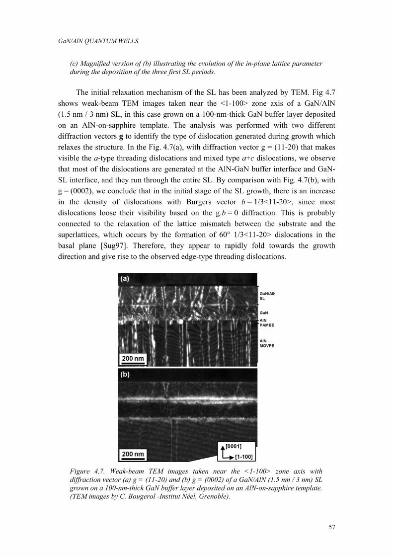
GaN/AlN QUANTUM WELLS
57
(c) Magnified version of (b) illustrating the evolution of the in-plane lattice parameter during the deposition of the three first SL periods.
The initial relaxation mechanism of the SL has been analyzed by TEM. Fig 4.7 shows weak-beam TEM images taken near the <1-100> zone axis of a GaN/AlN (1.5 nm / 3 nm) SL, in this case grown on a 100-nm-thick GaN buffer layer deposited on an AlN-on-sapphire template. The analysis was performed with two different diffraction vectors g to identify the type of dislocation generated during growth which relaxes the structure. In the Fig. 4.7(a), with diffraction vector g = (11-20) that makes visible the a-type threading dislocations and mixed type a+c dislocations, we observe that most of the dislocations are generated at the AlN-GaN buffer interface and GaN-SL interface, and they run through the entire SL. By comparison with Fig. 4.7(b), with g = (0002), we conclude that in the initial stage of the SL growth, there is an increase in the density of dislocations with Burgers vector b = 1/3<11-20>, since most dislocations loose their visibility based on the g.b = 0 diffraction. This is probably connected to the relaxation of the lattice mismatch between the substrate and the superlattices, which occurs by the formation of 60° 1/3<11-20> dislocations in the basal plane [Sug97]. Therefore, they appear to rapidly fold towards the growth direction and give rise to the observed edge-type threading dislocations.
Figure 4.7. Weak-beam TEM images taken near the <1-100> zone axis with diffraction vector (a) g = (11-20) and (b) g = (0002) of a GaN/AlN (1.5 nm / 3 nm) SL grown on a 100-nm-thick GaN buffer layer deposited on an AlN-on-sapphire template. (TEM images by C. Bougerol -Institut Néel, Grenoble).

STRAIN RELAXATION IN GaN/AlN SUPERLATTICES
58
From the data in Fig. 4.6, we conclude that the SLs evolve towards the same final strain state (average in-plane lattice parameter a ≈ 3.120 Å, for structures grown on both GaN and AlN templates. This has been verified ex-situ by XRD, where the lattice parameters were determined using the ω-2θ scan of the (0002) reflection and the reciprocal space map (RSM) around the (10-15) reflection of the SL. Figure 4.8 shows the (10-15) reflection of identical GaN/AlN SLs grown simultaneously on four different templates (GaN, AlN, Al0.35Ga0.65N and Al0.65Ga0.35N) on sapphire. Several SL satellite reflections have been detected indicating excellent periodicity of the layers. Also, we observe a shift in the alignment of the satellite reflections away from the reflection from the buffer, indicating partial relaxation of the structure. The values of lattice parameters extracted from XRD summarized in Table 4.II are consistent with the RHEED results and confirm that the difference in the average lattice constants between the SLs is smaller than 0.04%, to be compared to the 2.5% in-plane lattice mismatch between GaN and AlN.
Figure 4.8. Reciprocal space map around the asymmetric (10-15) x-ray reflection of GaN/AlN SLs grown on (a) GaN and (b) AlN templates.
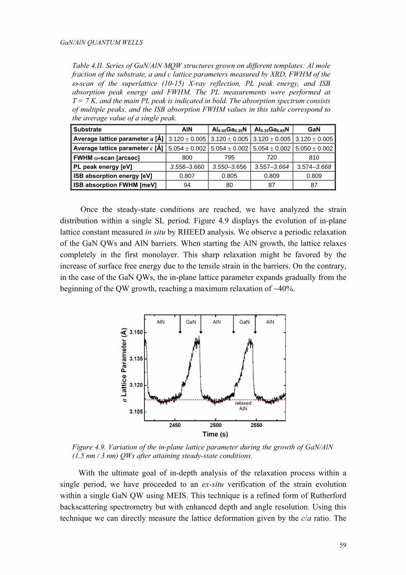
GaN/AlN QUANTUM WELLS
59
Table 4.II. Series of GaN/AlN MQW structures grown on different templates: Al mole fraction of the substrate, a and c lattice parameters measured by XRD, FWHM of the ω-scan of the superlattice (10-15) X-ray reflection, PL peak energy, and ISB absorption peak energy and FWHM. The PL measurements were performed at T = 7 K, and the main PL peak is indicated in bold. The absorption spectrum consists of multiple peaks, and the ISB absorption FWHM values in this table correspond to the average value of a single peak. Substrate AlN Al0.65Ga0.35N Al0.35Ga0.65N GaN Average lattice parameter a [Ǻ] 3.120 ± 0.005 3.120 ± 0.005 3.120 ± 0.005 3.120 ± 0.005 Average lattice parameter c [Ǻ] 5.054 ± 0.002 5.054 ± 0.002 5.054 ± 0.002 5.050 ± 0.002 FWHM ω-scan [arcsec] 800 795 720 810 PL peak energy [eV] 3.556–3.660 3.550–3.656 3.557–3.664 3.574–3.668 ISB absorption energy [eV] 0.807 0.805 0.809 0.809 ISB absorption FWHM [meV] 94 80 87 87
Once the steady-state conditions are reached, we have analyzed the strain distribution within a single SL period. Figure 4.9 displays the evolution of in-plane lattice constant measured in situ by RHEED analysis. We observe a periodic relaxation of the GaN QWs and AlN barriers. When starting the AlN growth, the lattice relaxes completely in the first monolayer. This sharp relaxation might be favored by the increase of surface free energy due to the tensile strain in the barriers. On the contrary, in the case of the GaN QWs, the in-plane lattice parameter expands gradually from the beginning of the QW growth, reaching a maximum relaxation of ~40%.
Figure 4.9. Variation of the in-plane lattice parameter during the growth of GaN/AlN (1.5 nm / 3 nm) QWs after attaining steady-state conditions.
With the ultimate goal of in-depth analysis of the relaxation process within a single period, we have proceeded to an ex-situ verification of the strain evolution within a single GaN QW using MEIS. This technique is a refined form of Rutherford backscattering spectrometry but with enhanced depth and angle resolution. Using this technique we can directly measure the lattice deformation given by the c/a ratio. The

STRAIN RELAXATION IN GaN/AlN SUPERLATTICES
60
experiment involves a set-up where a beam of mono-energetic 200 keV He+ ions is impinged at an angle ~ 74° to the sample surface. The energy and angular distribution of the scattered protons are measured simultaneously using a 2D detector with an energy resolution ∆E/E = 3×10⁻³ and an angular resolution of 0.1°, allowing deformation measurements with monolayer resolution. The scanning geometry was chosen in order to observe a range of ±10° around the [1-101] direction in the (11-20) plane. We focus on the energy range corresponding to interaction with Ga atoms.
[1-101][1-101]
Figure 4.10. (a) Energy/angular diffusion spectrum of He+ ions on the gallium atoms from the three upper GaN QWs, (b) Angular cut of figure (a) showing the blocking dip due to the [1-101] atomic column shadowing the diffusion. Measurements performed in collaboration with Dr. D. Jalabert (CEA-Grenoble).
The energy/angular distribution of ions are given in Figure 4.10 along with the detection yield. The histogram represents only scattering from Ga atoms in the GaN QWs because of the energy window. The image shows three reflections from the three topmost GaN QWs. Each reflection occurs in three different energies indicating the energy loss of the back scattered ions escaping out of the material: reflections located at lower energies come from deeper QWs. The reflections show several discontinuities with low yield, which are a consequence of the shadowing effect of Ga atoms present along various crystallographic directions. To get better resolution we have chosen the

GaN/AlN QUANTUM WELLS
61
blocking dip with minimum yield at about 62° for further analysis, which corresponds to Ga atoms in the [1-101] axis. On close observation we notice a shift in the blocking dip towards larger angles for lower energies within the top-most QWs, indicative of change in strain state along each GaN QW. The quantitative information on strain relaxation can be deduced experimentally from the c/a ratio, extracted from the angular position of the Ga [1-101] blocking dip, θ[1–101] using the equation [Jal05]
3tan ]1011[ a
c=⎟
⎠⎞
⎜⎝⎛ π
−θ+θ − 2i (4.4)
where θi is the incident beam angle. Assuming purely biaxial deformation we can calculate the in-plane lattice parameter a from the relationship:
xxzz ε−
=ε33
132C
C (4.5)
where εzz and εxx are the strain along the [0001] and [11-20] axes, respectively, and Cij are the elastic constants. Applying equations (4.4) and (4.5) to the MEIS results in Figure 4.10 we obtain the evolution of the in-plane lattice parameter along the growth axis within a single QW, as illustrated in Figure 4.11. These results are consistent with the above-described RHEED measurements as each consecutive reflections show the same shift in angle, confirming a periodic relaxation in the SLs.
Figure 4.11. Depth profile of the in-plane lattice parameter within one QW along the growth direction, extracted from the MEIS measurements in Fig. 4.10.
The above-described measurements with RHEED and MEIS confirm periodic relaxation with credible evidence, but the cause of this periodic relaxation is yet to be identified. The periodic relaxation mechanism has been analyzed by high-resolution transmission electron microscopy (HRTEM). HRTEM images of the SL structure taken along <11-20> zone axis (Fig. 4.12) show uniform periodicity of the layers. A sharp and abrupt interface at the atomic layer scale is a common site all through the structure, with no interdiffusion of AlN-GaN. However, when we zoom in to see the

STRAIN RELAXATION IN GaN/AlN SUPERLATTICES
62
finer details of the atomic arrangement, we notice defects at the interfaces: In the magnified image of the SL presented in Fig. 4.13(a) we observe stacking faults (SFs) in the AlN barriers.
Figure 4.12. High-resolution cross-sectional TEM image of a GaN/AlN (1.5 nm / 3 nm) SL taken along the <11-20> zone axis. (TEM images by C. Bougerol –Institut Néel, Grenoble).
A schematic description of the defect structure is presented in Fig. 4.14 for projections along the [11-20] and [0001] directions. At the first GaN/AlN interface [A in Fig. 4.13(a)], a basal stacking fault (BSF) of type I1, with a fault translation vector
61 <20-23>, intersects a 11-20 prismatic stacking fault (PSF). The prismatic fault boundary corresponds to the Drum atomic model [Dru65] (displacement vector = 2
1 <10-11>), as shown earlier by high resolution electron microscopy in GaN layers [Ver99]. The stair rod dislocation at the crossover of the BSF and the PSFs has a Burgers vector 6
1 <10-11> [Rut01]. At the second interface [B in Fig. 4.13(a)], we observe another 6
1 <10-11> stair rod dislocation, in the opposite sense that the first one. The SF loop closes creating clusters with a length of tens of nanometers, as the example illustrated in Fig. 4.15. Strictly speaking, the above-described structure is not equivalent to a misfit dislocation. However, the in-plane component of the defect contributes to strain relaxation by the introduction of half an m plane, marked with white circles in the filtered image in Fig. 4.13(c).
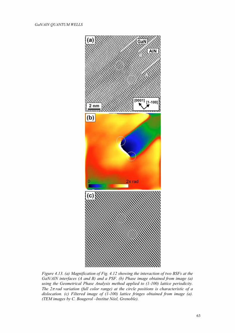
GaN/AlN QUANTUM WELLS
63
Figure 4.13. (a) Magnification of Fig. 4.12 showing the interaction of two BSFs at the GaN/AlN interfaces (A and B) and a PSF. (b) Phase image obtained from image (a) using the Geometrical Phase Analysis method applied to (1-100) lattice periodicity. The 2π rad variation (full color range) at the circle positions is characteristic of a dislocation. (c) Filtered image of (1-100) lattice fringes obtained from image (a). (TEM images by C. Bougerol –Institut Néel, Grenoble).

STRAIN RELAXATION IN GaN/AlN SUPERLATTICES
64
Figure 4.14. Schematic description of the defect structure identified in Fig. 4.13(b), projected along (a) the <11-20>axis and (b) the [0001] axis.
It is known that during the growth of wurtzite GaN, planar faults can be generated at interfaces [Ver99, Rut01, Tan95]. The strain fields induced by the heteroepitaxial growth of GaN or AlN on various substrates [6H-SiC, (0001) sapphire or (-1-1-1)B GaP] may lead to 11-20 PSFs [Dru65, Ver99, Rut01, Sve95, Rut99], which eventually form closed domains [Dru65, Sve95]. These SFs predominantly follow the Drum atomic model, which was found to be the more stable atomic configuration for GaN [Sve95, Xin97]. In the case of AlN, both the Drum and the
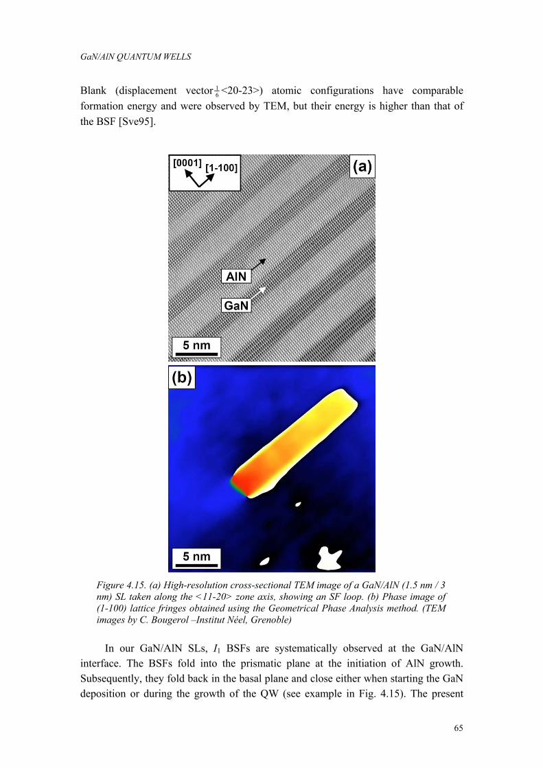
GaN/AlN QUANTUM WELLS
65
Blank (displacement vector 61 <20-23>) atomic configurations have comparable
formation energy and were observed by TEM, but their energy is higher than that of the BSF [Sve95].
Figure 4.15. (a) High-resolution cross-sectional TEM image of a GaN/AlN (1.5 nm / 3 nm) SL taken along the <11-20> zone axis, showing an SF loop. (b) Phase image of (1-100) lattice fringes obtained using the Geometrical Phase Analysis method. (TEM images by C. Bougerol –Institut Néel, Grenoble)
In our GaN/AlN SLs, I1 BSFs are systematically observed at the GaN/AlN interface. The BSFs fold into the prismatic plane at the initiation of AlN growth. Subsequently, they fold back in the basal plane and close either when starting the GaN deposition or during the growth of the QW (see example in Fig. 4.15). The present

STRAIN RELAXATION IN GaN/AlN SUPERLATTICES
66
behavior of the I1 BSF might seem in contradiction with the fact that the formation energy of PSFs is lower in GaN than in AlN [Rut99, Nor98, Sta98]. However, if we keep in mind that PAMBE is far from thermodynamic equilibrium, during the synthesis of AlN, the mobility of Al adatoms is particularly low at the growth temperature. This kinetic factor may overcome the energetic balance and favor the formation of the PSFs in the barriers. The same PSFs do not extend into the GaN layer because the growth is performed at Ga desorption temperature, granting higher mobility of the Ga species. An increase of the substrate temperature might result in a reduction in the defect density, but it would imply a dramatic degradation of the GaN/AlN interfaces [Gog04].
If we now consider the amount of strain relaxation, the total theoretical shift along the (11-20) direction introduced by a Drum-configuration PSF is 0.5a. Therefore, in order to attain the observed periodic relaxation (the variation measured by RHEED and MEIS is 1%) only via SFs, the density of these defects should be around 2–3 times what we observe by TEM. However, it has been reported that in the presence of stress, the deviation of the SF atomic structure from theoretical models can be significant, and the observed over-relaxation may probably originate from dislocations located in the PSF plane [Kre00].
4.5 Optical properties of GaN/AlN superlattices
The fundamental interband transition in MQW samples was probed by means of photoluminescence (PL) spectroscopy, to assess the internal electric field in the QWs. As described in chapter 4.2, the e1-h1 transition is particularly sensitive to the electric field due to the quantum-confined Stark effect (QCSE). Then, the electronic structure was analyzed using Fourier transform infrared spectroscopy (FTIR).
4.5.1 Interband characterization Figure 4.16 shows the low temperature (T = 7 K) PL spectra of GaN/AlN MQW
structures with 3-nm-thick AlN barriers and QW nominal thickness varying from 1.0 to 2.5 nm (4 to 10 ML). As expected, the PL peak energy is blue shifted by the quantum confinement in the thinner QWs (~1 nm) and strongly red shifted when increasing the QW thickness because of the QCSE.

GaN/AlN QUANTUM WELLS
67
3.0 3.5 4.0 4.5
440 400 360 320 280
7 ML9 ML 4 ML5 ML
Nor
mal
ized
PL
Inte
nsity
Energy (eV)
GaN
3 ML
10 ML
T = 7 K
Wavelength (nm)
Figure 4.16 Low-temperature (T = 7 K) normalized PL spectra of GaN/AlN MQW structures with 3-nm-thick AlN barriers and different GaN QW thickness.
An important feature of the PL spectra is the presence of non-periodical peaks or shoulders (see Fig. 4.16), which are located approximately at the same energies in the different samples and cannot be attributed to Fabry-Perot interferences. These discrete energy positions correspond to the expected values of the e1-h1 line in QWs whose thickness is equal to an integer number of GaN monolayers. For the very narrow QWs analyzed in this study, a variation of the thickness by 1 ML implies an important shift of the PL (about 150 meV for QWs of 4-5 ML). This value is larger than the FWHM of the PL lines, and hence results in well-resolved PL peaks instead of broadening the emission lines. It has been confirmed that these thickness fluctuations are related to structural defects (dislocations or eventually cracks) [Kan08].
4.5.2 Intersubband characterization Experiments were performed at the University Paris-Sud, under the supervision
of Prof. F. H. Julien. The ISB absorption of a series of 20-period Si-doped AlN/GaN MQW structures with ~ 3 nm AlN barriers and different GaN QW thickness was investigated using FTIR [Tch06]. As an example, Fig. 4.17 shows the ISB absorption of Si-doped AlN/GaN MQWs with QW thickness of 5 ML, 6 ML, 7 ML and 9 ML. The samples show a pronounced TM-polarized absorption, attributed to the transition from the first to the second electronic levels in the QW (e1→e2), while no absorption was observed for TE-polarized light within experimental sensitivity. The linewidth of the absorption remains in the 70-120 meV range for QWs doped at 5 × 1019 cm-2, and the ISB absorption efficiency per reflection attains 3-5%. A record small linewidth of ~ 40 meV has been achieved in non-intentionally doped structures.

OPTICAL PROPERTIES OF GaN/AlN SUPERLATTICES
68
The ISB absorption maximum can be tuned in the 1.33 to 1.91 µm wavelength range by changing the QW thickness from 4 ML to 10 ML. For large QWs (>8 ML), the e1→e3 transition is observed, as indicated in Fig. 4.17. This transition is allowed in nitride QWs because of the internal electric field in the well that breaks the symmetry of the potential. As observed in the PL measurements, the ISB absorption spectra present in general a multi-peak structure, which can be attributed to monolayer thickness fluctuations [Tch06].
0.4 0.6 0.8 1.0 1.2 1.4
0.0
0.4
0.8
1.2 3 2.5 2 1.5 1
e1-e2
e1-e3
9 ML 7 ML 6 ML 4 ML
Nor
mal
ized
ISB
abs
orpt
ion
Energy (eV)
Wavelength (µm)
Figure 4.17. Room-temperature TM-polarized ISB absorption spectra from Si-doped GaN/AlN MQW structures with 3-nm-thick AlN barriers and different GaN QW thickness.
a) Effect of the stacking faults
Use of III-N materials for opto-electronic and electronic devices requires a clear knowledge of the role played by the defects in the material. For instance, it is known that threading dislocations behave as non-radiative recombination centers. Theoretical investigations of the electronic structure of SFs in III-nitrides reveal that they do not introduce localized states in the band gap [Sta98]. However, the local increase of the lattice symmetry can distort the electronic structure, giving rise, for instance, to luminescence lines below the wurtzite band gap [Liu05], around 3.40 eV and 3.2 eV for BSFs and PSFs, respectively. I have analyzed the effect of the observed stacking faults on the optical properties of the GaN/AlN SLs using the Nextnano3 8×8 k.p Schrödinger-Poisson solver with the material parameters described in Ref. [Kan08]. For such simulations, I have considered the effect of two BSFs located at the GaN/AlN and AlN/GaN interfaces of a QW, neglecting the role of PSFs. The effect of PSFs on the electronic levels is expected to be negligible since they are perpendicular to the heterointerfaces. On the contrary, a BSF implies the introduction of a monolayer of cubic sequence along the [0001] axis. The local enhancement of the crystal symmetry should result in a cancelation of the spontaneous polarization of the crystal at the interfaces, which should ultimately reflect in a shift of the ISB energy distance.

GaN/AlN QUANTUM WELLS
69
Figure 4.18 presents the results of the simulation of the electronic structure of a defective QW, with the following assumptions:
(a) Ideal GaN/AlN SL without SFs (b) SL with 1 ML of cubic AlN at each interface of the barrier (c) SL with 1 ML of cubic GaN at each interface within the QW
Figure 4.18. Electronic band structure of a GaN QW in a SL with 3-nm-thick AlN barriers and 1.5-nm-thick GaN QWs assuming (a) ideal conditions, (b) SL with 1 ML of AlN with zero spontaneous polarization at each interface, and (c) SL with 1 ML of GaN with zero spontaneous polarization at each interface within the QW.
We can notice that the cancelation of the spontaneous polarization in the AlN has a significant influence on the band diagram due to the local inversion of the electric field [Fig. 4.18(b)]. The result is approximately equivalent to a reduction of the conduction band offset between GaN and AlN. We observe an important energy shift and charge redistribution regarding the third electronic level, e3. However, the second electronic level remains almost undisturbed, and the difference e2-e1 is only reduced by 17 meV. On the other hand, 1 ML of GaN with zero polarization at the interfaces [Fig. 4.18(c)] shows barely noticeable change in the band structure compared to the ideal SL. On comparing the e2-e1 transition energy for the three different situations, we find an ideal value of 81 meV, which is reduced by 17 meV in case (b) and increased by 1.1 meV in case (c). If we compare these deviations to the linewidth of the ISB absorption (~ 80 meV) or with the energy shift resulting for one monolayer thickness fluctuation of the QW (~ 100 meV), we conclude that the optical energy shift associated to the presence of stacking fault loops is negligible. However, the electrical activity of this kind of defects is still to be determined.
b) Effect of the substrate
We have characterized GaN/AlN (1.5 nm / 3 nm) SLs grown on four different templates (AlxGa1-xN where x= 0, 0.65, 0.35 and 1) using the FTIR set-up. Absorption peaks plotted in Fig. 4.19, of all the structures fall at the same energy 0.8 eV (1.55 µm) irrespective of the templates used for growth. This result is in excellent agreement with the inference, about strain state of the structure extracted from the data obtained by

OPTICAL PROPERTIES OF GaN/AlN SUPERLATTICES
70
RHEED, XRD, TEM and MEIS. The FWHM of the peaks is maximum for AlN template because of high threading dislocation density in the template which is passed on to SL structure. The shoulders in the absorption peaks are attributed to monolayer fluctuations, shifting the absorption energy beyond the normal FWHM of ~ 80 meV.
0.6 0.8 1.0 1.2
0.0
0.2
0.4
0.6
0.8
1.0
2.4 2 1.6 1.2
N
orm
aliz
ed A
bsor
ptio
n
Energy (eV)
x = 0 x = 0.35 x = 0.65 x = 1
AlxGa1-xN Substrate
Wavelength (µm)
Figure 4.19. Room-temperature TM-polarized ISB absorption spectra from Si-doped GaN/AlN (1.5 nm / 3 nm) SLs grown on various AlxGa1-xN-on-sapphire templates.
c) Effect of the cap layer: Polarization-induced doping
In nitride heterostructures, the magnitude of the ISB absorption depends not only on the Si doping level in the QWs, but also on the presence of non-intentional dopants and on the carrier redistribution due to the internal electric field. In order to evaluate the contribution of the internal electric field induced by the cap layer to the ISB absorption, I have synthesized a series of 40-period non-intentionally doped GaN/AlN (1.5 nm / 3 nm) SLs where I varied the Al mole fraction of the 50-nm-thick AlxGa1−xN cap layer. All the structures were grown on AlN-on-sapphire templates.
Sample Al mole fraction in the cap layer
ISB absorption (FWHM) [eV]
Absorption per reflection [%]
E1487 100% 0.797 (0.080) 1.7 E1488 65% 0.787 (0.040) 0.26 E1489 35% 0.781 (--) 0.15 E1486 0% -- <0.005
Table 4.III. Series of non-intentionally doped GaN/AlN (1.5 nm / 1.5 nm) MQW structures capped with 50 nm of AlxGa1-xN with different Al mole fraction.
Measurements of ISB absorption in these samples, summarized in Fig. 4.20 and Table 4.III, confirm a monotonous increase and broadening of the absorption when increasing the Al mole fraction of the cap layer. These results are consistent with the simulations of the electronic structure in Fig. 4.21, where we observe that the use of AlN as a cap layer lowers the conduction band of the first GaN QWs below the Fermi

GaN/AlN QUANTUM WELLS
71
level (dash-doted line at 0 eV in the figures), whereas the use of GaN as a cap layer results in the depletion of the MQW active region. Therefore, we conclude that the internal electric field induced by the cap layer can result in a significant (even dominant) contribution to the infrared absorption in GaN/AlN SLs.
0.6 0.8 1.0 1.2
10-2
10-1
100
2 1.8 1.6 1.4 1.2
AlN Al0.65Ga0.35N Al0.35Ga0.65N GaN
Abs
orpt
ion
per p
ass
(%)
Energy (eV)
Wavelength (µm)
Cap Layer
Figure 4.20. Room temperature TM-polarized ISB absorption spectra of non-intentionally doped GaN/AlN (1.5 nm / 1.5 nm) MQW structures finished with a 50 nm thick AlxGa1-xN cap layer with different Al mole fraction.
Figure 4.21. Band diagram of non-intentionally doped GaN/AlN (1.5 nm / 1.5 nm) MQW structures with (a) AlN cap layer and (b) GaN cap layer.

OPTICAL PROPERTIES OF GaN/AlN SUPERLATTICES
72
4.6 Semipolar GaN/AlN superlattices
The already high design complexity in terms of modeling ISB devices like quantum cascade structures further increases with the large polarization-induced internal electric field in c-plane polar III-N heterostructures. Polarization effects can be eliminated by using heterostructures based on nonpolar crystallographic orientations, such as m-plane 1-100 or a-plane 11-20, which exhibit no electric field. However, growth of nonpolar III-nitrides remains challenging due to the strong anisotropy of the surface properties [Fun06], resulting in epitaxial layers with a high density of crystalline defects. An alternative approach is the growth on semipolar planes, which are those (hkil) planes with a nonzero h, k or i and a nonzero l Miller index.
In the laboratory, there has been an effort to optimize the growth of III-nitride heterostructures grown on the (11-22) semipolar plane [Lah07, Lah08, Lah08b]. This crystallographic orientation is obtained by deposition of AlN on m-sapphire under slightly N-rich conditions [Lah07]. The synthesis of semipolar (11-22) GaN/AlN SLs has been demonstrated [Lah08b] by Dr. L. Lahourcade, and I have participated to the optical characterization and theoretical interpretation of the results, in order to identify the precise role of the internal electric field on the ISB transition energies. The results were analyzed by comparison to polar GaN/AlN SLs, which served as a reference.
The simulations of the SL structure were performed using the Nextnano3 tool with the parameters described in section 4.2, but changing the [hkil] axis along the z direction to [6 6 -12 7], axis approximately perpendicular to the (11-22) plane. The band structure of GaN/AlN QW of semi-polar and polar orientations strained on GaN and AlN are compared in Fig. 4.22.
-4
-2
0
2
4
e3e2e1
Strained on GaN
Ener
gy (e
V)
Strained on AlN
[0001]h1
-4
-2
0
2Strained on GaN
Ener
gy (e
V)
Strained on AlN
⊥(11-22)
Figure 4.22. Simulated band profile of GaN/AlN (2.5 nm / 5 nm) polar and semipolar QWs strained on GaN and AlN.
In the case of polar structures the electric-field is approximately 6.7 MV/cm and 8 MV/cm for QWs strained on AlN and GaN respectively. The higher electric-field in QWs strained on GaN is due to large piezoelectric constants in the barrier. On the contrary, the semipolar structures exhibit quasi-square potential profiles with symmetric wavefunctions due to the reduced electric field of 0.6 MV/cm and -0.55 MV/cm for QWs strained on AlN and GaN, respectively. The significant reduction in the internal electric field is due to the fact that the spontaneous and

GaN/AlN QUANTUM WELLS
73
piezoelectric polarization differences at the interfaces have opposite signs, the piezoelectric component being dominant in SLs strained on GaN (negative electric field).
1.0 1.5 2.0 2.5 3.0
2.5
3.0
3.5
4.0
Polar
e 1-h1 E
nerg
y (e
V)
QW Thickness (nm)
Strained on AlN Strained on GaN
T = 7 K
Semipolar
Figure 4.23. Comparison of e1-h1 transition energy of polar and semipolar QWs as a function of well width. The dots correspond to the experimental measurements.
Figure 4.23 displays the change in the e1-h1 transition energy as a function of the QW thickness, strain state and crystallographic orientation: polar and semipolar. The considerable red-shift in polar SLs with increasing well thickness is caused by the QCSE, whereas in the semipolar structures the range of energy deviation with thickness is comparatively short. The strain-related shift in semipolar structures is mostly due to the variation of the GaN band gap. In the case of polar SLs, the variation of the piezoelectric field imposes an additional contribution to the transition shift. The experimental PL measurements fit well the theoretical calculations in the case of polar SLs, where the in-plane lattice parameters lies close to the one of AlN (see strain analysis in the previous section). In the case of semipolar SLs, a good fit is obtained when assuming the structures strained on GaN. However, a precise determination of the strain state of the structures was not possible due to the broadening of the XRD reflections and the error bars of the measurements.
The evolution of ISB transition energy with well thickness is represented in Fig. 4.24. In polar SLs, the ISB energy decreases with increase in well width influenced by electric field, but quantum confinement is the only dominant factor in the case of semipolar SLs. To perform ISB characterization of the semipolar structures, I used two samples with 40 periods of GaN/AlN, consisting of 2 nm and 2.5 nm thick GaN QWs with 3nm thick AlN barriers. The whole structure was deposited on a 280 nm thick GaN grown on a 150 nm thick AlN buffer directly on m-sapphire. The e1-e2 transition was probed by photo-induced absorption using FTIR. Carriers to populate the first electronic level were generated by excitation with a 244 nm Ar laser. The TM-polarized absorption spectra are represented in Fig. 4.25. No absorption was observed for TE-polarized light within our experimental accuracy, which is a signature

SEMIPOLAR GaN/AlN SUPERLATTICES
74
of an ISB transition between electron states confined in the QWs. These results confirm that the polarization-induced internal electric field in GaN/AlN heterostructures induces a blue shift of the ISB transitions in polar materials. The absorption FWHM is ≈ 80-110 meV comparable to the polar structures. For larger QWs, the ISB absorption is not observable by this technique due to the onset of absorption by the sapphire substrate.
1.0 1.5 2.0 2.5 3.0
0.4
0.6
0.8
1.0
Semipolar
Strained on AlN Strained on GaN
e 1-e2 (e
V)
QW Width (nm)
Polar
Figure 4.24 Variation of e1-e2 energy as a function of well width in polar and semipolar QWs strained on GaN and AlN.
0.2 0.3 0.4 0.5 0.6 0.7
8 7 6 5 4 3 2
2.5 nm
Nor
mal
ized
PIA
Energy [eV]
2.0 nm
Wavelength [µm]
Figure 4.25 Photo-induced absorption (PIA) spectra of GaN/AlN SLs with 2nm and 2.5nm QW thickness.
4.7 ConclusionsI have studied the effect of PAMBE growth and design parameters on the
performance of Si-doped GaN/AlN QW SLs for ISB optoelectronics in the NIR

GaN/AlN QUANTUM WELLS
75
spectral region. In order to optimize the growth parameters, we have systematically analyzed the misfit relaxation mechanisms. The use of a Ga excess during the growth of both GaN and AlN was found to play a crucial role in the relaxation process. The large misfit stress between the substrate and the SL is relaxed mostly by generation of edge-type threading dislocations. The final strain state of the superlattice, reached after 10-20 periods, is independent of the substrate (either GaN or AlN templates), which is reflected as substrate independent (GaN, AlN or AlGaN) ISB absorption energy.
Once the influence of the substrate becomes negligible, we observe a periodic partial relaxation of quantum wells and barriers. This phenomenon can be related to the presence of BSFs and PSFs that originate when starting the AlN deposition and close after deposition of the barrier forming loops with an in-plane length of tens of nanometers. However, the presence of stacking faults is predicted not to cast much influence on the ISB transition energy, as their effect is within the broadening limit.
Finally, I have studied the effect of the polarization-induced internal electric field on the ISB absorption. The polarization discontinuity due to the cap layer can induce the population or depletion of active QWs. The influence of capping layer on ISB absorption magnitude presented in this chapter has its implications on the design of waveguides and contact region for the complex structures. On the other hand, the reduction of the internal electric field results in red shift of the ISB transitions with respect to polar material. The experimental results in the semipolar GaN/AlN SLs are consistent with simulations of the electronic structure, which predict a reduction of the polarization-induced internal electric field by more than one order of magnitude.

CONCLUSIONS
76

Chapter 5
GaN/AlN quantum dots
In this chapter I present my contribution to the domain of GaN/AlN quantum dots (QDs). With the basis of the previous know-how, I have tried to drive this technology to new limits in terms of dilution and QD size minimization. The progress in QD growth has made it possible to perform spectroscopic studies demonstrating the absence of non-radiative recombination in long-lived GaN/AlN QDs. Finally, studies of the intraband performance of QD structures as a function of the QD density are also presented.
5.1 Introduction
Quantum dots (QDs) are zero-dimensional nanostructures exhibiting novel properties below a certain size limit. These nanostructures play an important role in improving performance of devices when incorporated in the active region. As a best example we have the quantum dot lasers proposed by Arakawa and Sakaki [Ara82]. These devices operate at low threshold current densities, and at the same time offer temperature stability in an ideal scenario. However, fluctuations in dot size and density in self-assembled nanostructures form a bottleneck hindering their use in commercial applications.
QDs also prove to be excellent candidates for intersubband (ISB) devices in comparison to quantum wells (QWs) because they exhibit sharp quantized levels without parabolic bands along kx and ky as in QWs. It has been previously observed that QDs indeed show longer lifetimes of excited state for mid-infrared (MIR) and far-infrared (FIR) spectral regions caused by the phonon bottleneck [Xin98]. The importance of longer excited-state lifetimes and efficient draining of carriers from the ground state is evident in quantum cascade lasers (QCLs), to obtain population inversion. Excited state lifetimes as long as 1.5 ns were observed by Zibik et al. [Zib09] at 14.5 meV transition energy between s and px states of InGaAs QDs, below the LO-phonon energy. However, the lifetime drastically reduces with increasing energy due to availability of different two-phonon disintegration channels. The extreme sensitivity of anharmonic behavior in this case is a consequence of three-dimensional (3D) carrier confinement, similar to extra lateral confinement provided by high magnetic fields for QW-based Terahertz QCLs [Wad09]. The proposal of QD-based QCLs has been reported [Win96], which allows reduction of number of multi-radiative stages due to increased gain.

INTRODUCTION
78
GaN QDs exhibit several attractive properties stemming from the large exciton binding energy [Pet98] and strong carrier localization. Large exciton binding energies of 27 meV allow observation of excitonic effects even at room temperature, mostly a consequence of large effective mass in GaN.
GaN/AlN QDs have the shape of truncated pyramids, this allows excited states with both in-plane and vertical confinement components, behaving in a different manner in comparison to lens shaped QDs [Gab05]. The most dominating dipole in InGaAs (lens shaped) quantum dots is in-plane allowing normal incidence absorption in contradiction to z-direction dipoles for GaN QDs. The GaN QDs embedded between AlN layers exhibit strong TM-polarized absorption in the NIR for transitions from s to pz states. The absorption wavelength can be tuned to shorter wavelengths by reducing the height which falls at ≈ 1.2 nm for absorption at 0.8 eV. In terms of devices, quantum dot infrared photodetectors (QDIPs) based on lateral conduction have been demonstrated [Doy05, Var06] with photocurrent peaked at λ = 1.41 µm at room temperature [Var06]. QD-based photovoltaic ISB photodetectors have also been demonstrated and their responsivity outperforms QW-based photodetectors with the same design [Dan10]. Finally, TM-polarized ISB photoluminescence (PL) at 1.48 µm from GaN/AlN QDs has been reported at room temperature [Nev08].
The main motivation of the chapter lies in the growth of GaN/AlN QDs with controlled density, even for the small QDs required for ISB transitions at 1.5 µm (height ~ 1 nm). The progress I achieved in the understanding of the GaN QD growth has been applied to a number of spectroscopic studies by our collaborators in Grenoble and in Technion (Israel).
5.2 Growth of GaN/AlN QDs
5.2.1 Growth conditions: N rich vs. Ga rich
The growth of GaN quantum wells on AlN is subject to Ga excess conditions to minimize the (0001) surface energy. Roughening is inhibited and the elastic energy is released by formation of misfit dislocations after a certain critical thickness. The formation of 3D structures requires an enhancement of the (0001) surface energy, to favor the relaxation by faceting over the relaxation by dislocations. There are two methods to grow GaN QDs on AlN by PAMBE: either by GaN deposition under N-rich conditions [Gui06] or by GaN deposition under Ga-rich conditions followed by a growth interruption [Gog04, Dam99, Bro04]:
− N-rich conditions: The QD growth is performed at III/V ratio below 1, which increases the surface energy of the (0001) plane [Neu03] and hence favors the formation of 3D faceted structures. Under these conditions, growth starts two dimensional until the deposition of a 2-ML-thick wetting layer. Due to the

GaN/AlN QUANTUM DOTS
79
lattice mismatch between AlN and GaN, further GaN deposition leads to the formation of 3D islands (Stranski-Krastanov growth mode) [Dau97, Gui06]. The QD formation can be monitored by RHEED, which shows a rapid increase of the a-axis lattice parameter and of the RHEED intensity, with appearance of a spotty RHEED pattern with reflections corresponding to the QD facets. N-rich growth implies a low mobility of adatoms on the surface, which generally, results in a high density (1011-1012 cm-2) of small QDs (1-2 nm high).
− Ga-rich conditions followed by a growth interruption: In this method a GaN layer is grown under Ga excess following the Frank-van der Merwe growth mode. The layer rearranges into 3D nanostructures during a growth interruption under vacuum. Although QDs form when the Ga excess is completely evaporated, the rearrangement of adatoms commences before, taking place even when the Ga is on its way towards complete desorption from the surface. The higher mobility of adatoms under Ga rich conditions result is a lower QD density (1010-1011 cm-2) and bigger QDs (2-5 nm high).
Figure 5.1 presents typical atomic force microscopy (AFM) images of GaN QDs grown under (a) N-rich conditions and (b) Ga-rich conditions, deposited on AlN at a substrate temperature of 720°C. Cross-section TEM images of the samples show in dynamic contrast conditions the larger and smaller QDs in Fig. 5.2. We can observe that the QD geometry achieved under Ga-rich conditions favors the vertical correlation of the QDs in a stack.
Figure 5.1. Typical AFM images of GaN QDs grown under (a) N-rich conditions and (b) Ga-rich conditions.

GROWTH OF GaN/AlN QUANTUM DOTS
80
Figure 5.2: Cross-section TEM bright-field images showing 40 period GaN/AlN QD superlattices grown under N-rich conditions (left) and under Ga-rich conditions (right). (TEM images from Prof. Ph. Komninou, Aristotle University of Thessaloniki)
In all the cases, GaN QDs are hexagonal truncated pyramids with 1-103 facets [Cha04], and no Ga-Al interdiffusion has been observed [Sar05]. The QDs can be n-type doped by incorporating a silicon flux during the GaN deposition, without modification of their structural properties [Gui06]. The QD dimensions and density can be tuned by varying the amount of GaN contained in the QD layer, the growth temperature, or the growth interruption time after deposition of the QDs (ripening effect) [Gui06].
One of the targets of this study was to control the density of QDs with interband absorption around 1.5 µm, i.e. QD height around 1 nm. This implies either reducing the QD density in the case of N-rich growth or reducing the QD size in the case of Ga-rich growth. Both approaches are addressed in this thesis.
5.2.2 QD dilution under N-rich conditions
In order to dilute GaN QDs grown under N-rich conditions, I tried varying the substrate temperature, TS, and the GaN deposition time, tGaN. For this experiment, a single GaN QD layer was deposited on an AlN-on-sapphire template using a Ga-limited growth rate of 0.25 ML/s, corresponding to a Ga/N ratio = 0.9. Prior to the QD growth, I deposited about 50 nm of AlN. The GaN QD formation was followed by a growth interruption under vacuum (GIV) for 2 min, after which the sample was cooled down by switching off the current of the substrate heater.
To systematically quantify the evolution of QD size and density, in a first series, I varied the substrate temperature while keeping the GaN deposition time constant: tGaN = 13 s. The samples were grown at 718°C, 738°C and 758°C respectively. The

GaN/AlN QUANTUM DOTS
81
AFM measurements on these samples, presented in Fig. 5.3, show high density of QDs for the lowest Ts of 718oC which reduces with increasing temperature. However, at higher temperatures the QDs are not well formed and display very broad size distribution where the very tiny spots indicate the nucleation centers and not the QDs. The nucleation centers remain stable even after 2 min of ripening under vacuum. This is probably due to low mobility of Ga-N species for N-rich surface conditions. This problem can be avoided by increasing the Ts to enhance the mobility.
Figure 5.3. AFM images of GaN QDs grown at (a) Ts = 718°C, (b) Ts = 738°C, and (c) Ts = 758°C.
As a next step, I repeated the experiment keeping Ts constant at 778oC, while I varied the deposition time between tGaN = 15 s and tGaN = 11 s. For small tGaN, very small QDs at extremely low densities are observed, whereas increasing the time to 15 s relatively larger dots with moderately high density are formed, as depicted in Fig. 5.4. It must be noted that the size distribution is not drastically large. However, it is difficult to grow QD SLs for device applications because of the high substrate temperatures required to reach small dot height and density. At these high temperatures, the reaction between GaN and AlN [Gog04] makes it difficult to control and reproduce the QD size in a stack.
Figure 5.4. AFM images of GaN QDs obtained by deposition of (a) 15 s, and (b) 11 s of GaN at Ts = 778°C.

GROWTH OF GaN/AlN QUANTUM DOTS
82
5.2.3 Reduction of the QD size under Ga-rich conditions
In a first approach to reduce the QD size while growing under Ga-rich conditions, initially 10 s of Ga were supplied to wet the surface, and then keeping the Ga flux, N was supplied for few seconds, tN, to form GaN. Finally, the surface was allowed to evolve under vacuum for 2 min. The RHEED pattern which initially displays streaks (2D growth), changes spotty once the excess Ga on the surface is desorbed. In this process, tN and Ts decide the dot size and density, as the GIV must be above certain critical limit to desorb all the Ga excess and form the dots. Three samples where grown with Ts = 735°C, 733°C and 723°C, and at a constant tN = 6 s. As seen in Fig. 5.5, a considerable reduction in QD density is achieved when increasing the substrate temperature, with a complete inhibition of the QD formation at 735°C. The uniformity of the QD size and distribution is improved in comparison to N-rich growth. The dots in Fig. 5.5(b) have a height of 1.4 nm.
Figure 5.5. AFM images of GaN QDs grown at (a) Ts = 723°C, (b) Ts = 733°C, and (c) Ts = 735°C.
Using the above-described growth conditions 40 periods of GaN/AlN (1.5 nm / 3 nm) diluted QDs were grown, with the result illustrated in Fig. 5.6. We observe that the high mobility of Ga deposited under Ga-rich conditions favors the nucleation of the QDs in the minimum energy sites, i.e. next to threading dislocations. The QD dilution and their interaction with dislocations favor the vertical alignment of the QDs.

GaN/AlN QUANTUM DOTS
83
Figure 5.6. High-resolution TEM images of GaN/AlN (1.5 nm / 3 nm) QD SLs grown (left) under N-rich conditions and (right) Ga-rich conditions. (TEM images from Dr. E. Sarigiannidou, INPG).
5.3 Optical characterization
5.3.1 Interband characterization: QD vs. QW
The exciton localization due to large band offset in III-nitride QDs offers varied advantages. Due to the 3D electron confinement, excitons trapped in QDs are expected to be much more insensitive to nonradiative recombination than other semiconductor structures, for instance QWs [Ger96]. This difference should be particularly acute in semiconductors with high structural defect densities such as III-nitrides.
To clearly understand the recombination dynamics in GaN/AlN we must keep in mind the electron and hole wavefunction distribution. The electric field strongly separates the carriers: electrons are pushed up to reside on top of the QDs and holes sit almost near to the wetting layer right under the pyramidal structure, as illustrated in Fig. 5.7 [And01]. This effect is seen as a strong red shift of the emission energy, even below the band gap of bulk GaN.

OPTICAL CHARACTERIZATION
84
Figure 5.7. Probability density distribution for the electron and hole ground states for (a) a large dot (h ~ 3.6 nm) and (c) a small dot (h ~ 1.8 nm); darker areas indicate larger density values, solid lines mark the QD boundary. Lower plots show the conduction and valence band edge energies along a line through the QD center for (b) large and (d) small dots. Energies of the electron and hole ground state E1 and H1 are also shown. Insets in (b) and (d) show the z dependence of the probability density, for the electron and hole ground states (After Andreev et al. [And01]).
Typical room temperature PL spectra from GaN/AlN QDs are presented in Fig. 5.8. The samples consist of 40-period SLs with 7-nm-thick AlN barriers and various GaN QD sizes, consistent with the growth conditions summarized in Table 5.I. The quantum confinement blue shifts the PL of the smaller QDs, whereas the larger QDs, due to the quantum confined Stark effect (QCSE), show luminescence well below the GaN band gap.
Figure 5.8. Room-temperature PL spectra of the studied QD superlattices with varying QD heights. On the sides, high-resolution TEM images of the samples with larger and smaller QDs. (TEM images from Prof. Ph. Komninou, Aristotle University of Thessaloniki).

GaN/AlN QUANTUM DOTS
85
Sample Growth conditions Amount of GaN in the QD layer PL peak wavelengthE1759 N rich 4 ML 340 nm E1761 N rich 3 ML 310 nm E1762 Ga rich 5 ML 440 nm E1764 Ga rich 4 ML 420 nm
Table 5.I. Variation of the PL peak wavelength of GaN/AlN QD superlattices as a function of the growth conditions.
A signature of 3D carrier confinement in QD structures is the thermal stability of the PL [Lub95, Ade00]. Figure 5.9 compares the thermal quenching of the PL of a 40-period GaN/AlN QD stack and a GaN/AlN multiple-QW structure, both emitting around 450 nm. We observe a thermal quenching of the luminescence from the QDs of less than a factor of two from 10 K to room temperature, whereas, at the same temperature range, the QW luminescence drops by more than two orders of magnitude. The persistence of the luminescence signal is a signature of the 3D carrier confinement in GaN/AlN QD SLs.
10 100
10-4
10-3
10-2
10-1
100
100 10
QDs QWsNor
mal
ized
PL
Inte
nsity
1000 / T (K-1)
PL emission @ 450 nm
Temperature (K)
Figure 5.9. Thermal quenching of the PL from a 40-period GaN/AlN QD stack and from a 40-period GaN/AlN multiple QW sample, both emitting around 450 nm.
In addition to the spectral red shift, GaN/AlN QDs suffer from long radiative decay times that can reach the microsecond range [Bre06]. This happens mainly due to reduced overlap between the electron and hole wavefunctions. It is often argued that long radiative decay times are associated to low radiative quantum yields, this argument being commonly used to promote the utilization of nonpolar and semipolar heterostructures with attenuated internal electric field. However, 3D confinement in the QDs can significantly attenuate nonradiative recombination for low oscillator strength transitions. Therefore, I have grown a series of QD and QW superlattices to assess the efficiency of 3D confinement to inhibit nonradiative processes. These PL studies were performed by my colleague Dr. J. Renard [Ren09], under the supervision of Dr. B. Gayral.

OPTICAL CHARACTERIZATION
86
GaN/AlN QD and QW 40-period SLs with 7-nm-thick AlN barriers and various GaN QW/QD thicknesses were deposited on AlN-on-sapphire templates by PAMBE. The growth/geometry parameters are summarized in Table 5.II. The GaN/AlN QW structures were grown under Ga-rich conditions without growth interruptions, as described in chapter 4. The synthesis of polar GaN/AlN QDs was performed either by GaN deposition under N-rich conditions or by GaN deposition under Ga-rich conditions followed by a growth interruption. The samples display PL emission peak energy varying from 310 nm to 450 nm (i.e. QD height varying from 1 nm to 3 nm), as also summarized in Table 5.II.
Sample Growth conditions
Amount of GaN in the QD layer / QW thickness
PL wavelength
Decay time
QD-1 N rich 3 ML 310 nm 0.29 ns QD-2 N rich 4 ML 340 nm 0.7 ns QD-3 Ga rich 4 ML 400 nm 50 ns QD-4 Ga rich 5 ML 440 nm 500 ns QW-1 Ga rich 1.2 nm 310 nm 0.21 ns QW-2 Ga rich 1.7 nm 365 nm 2.8 ns QW-3 Ga rich 2.5 nm 415 nm 36 ns QW-4 Ga rich 3.0 nm 455 nm 285 ns
Table 5.II. Variation of the PL peak wavelength and low-temperature (5 K) PL decay time of GaN/AlN QD and QW superlattices as a function of their geometry/growth parameters.
In Table 5.II, we can observe that larger sized QDs emit at longer wavelengths and have longer PL decay times in comparison to smaller QDs. The radiative lifetime remains flat (shown in the inset) for the whole temperature range. Figure 5.10(a) displays the dramatic difference of the PL decay measured in sample QW-3 at room temperature and at 5 K. This result is to be compared to Fig. 5.10(b), which displays the behavior of GaN/AlN QDs (sample QD-4), showing thermal insensitivity in all the temperature range. Figure 5.11(a) illustrates the temperature dependence of the 1/e decay times measured on the four QW samples. The PL decay times are roughly constant up to 75 K, which strongly suggests that the decay is dominated by radiative recombination at low temperature. However, the decay times decrease significantly for higher temperatures -typically at least a factor of 2 is already lost at 150 K and at least a factor 10 at room temperature. This is valid for all samples, even for the ones presenting radiative decay times below 1 ns. In contrast, in the case of QD samples, illustrated in Fig. 5.11(b), the decay times remain constant as an indication of the inefficiency of nonradiative recombination paths in such structures. The most striking feature is that this is true even for QDs presenting radiative decay times of 500 ns as illustrated in the figure.

GaN/AlN QUANTUM DOTS
87
0 20 40 60 80 100 120 1400.01
0.1
1
Nor
mal
ized
PL
Inte
nsity
Time (ns)
T = 5 K T = 300 K
(a)
0 1000 2000 3000 40000.01
0.1
1
(b)Nor
mal
ized
PL
Inte
nsity
Time (ns)
T = 5 K T = 300 K
Figure 5.10. Comparison of the normalized PL decay at 5 K and room temperature for (a) a QW sample (QW-3), and (b) a QD sample (QD-4) [Ren09].
0 100 200 3000.01
0.1
1
10
100
Dec
ay T
ime
(ns)
Temperature (K)0 100 200 300
0.1
1
10
100
1000
D
ecay
Tim
e (n
s)
Temperature (K)
Figure 5.11. Evolution of the decay time of the PL as a function of the temperature for four (a) QW samples (QW-3), and (b) QD samples (QD-4) [Ren09].
Comparing the results on QWs and QDs, we can confirm that the nonradiative recombination of photogenerated carriers in the QDs is suppressed in the 4-300 K temperature range. From the data a lower limit non-radiative recombination life-time of 10 µs was estimated. This is mainly due to the large conduction band offset between GaN and AlN allowing strong vertical and lateral confinement of the carriers. These results are consistent with the temperature dependence of the integrated PL intensity from QDs and QWs described in Fig. 5.11.
5.3.2 Intraband characterization
For infrared absorption measurements, the samples are mechanically polished to form a 45° multi-pass waveguide with 4-5 total internal reflections. The infrared transmission for p- and s-polarized light was measured at room temperature using a Fourier transform infrared (FTIR) spectrometer and a deuterated triglycine sulfate (DGTS) photodetector. Measurements were performed at the University Paris-Sud, under the supervision of Prof. F. H. Julien. Typical transmission spectra are shown in
(a) (b)

OPTICAL CHARACTERIZATION
88
Fig. 5.12 for a sample with 20 periods of (~ 1.3 nm / 3 nm) GaN/AlN QDs grown under N-rich conditions [Gui06]. The low energy cutoff at about 0.3 eV is due to absorption by the sapphire substrate. A TM-polarized absorption peak appears at 0.81 eV, whereas the TE-polarized spectrum does not show any significant absorption in the spectral range under study, within experimental accuracy of our setup. The TM-polarization of the absorption peak implies that it originates from a transition with an optical dipole oriented perpendicular to the (0001) layer plane. The absorption is ascribed to the transition from the s-shell ground state of the QD to the pz excited state with one node of the envelope function along the growth axis. The transition energy in Fig. 5.12 is close to the energy measured for the e1-e2 ISB absorption in 5-6 ML (1.25-1.5 nm) thick GaN/AlN QW SLs [Hel03]. This confirms that the energy of the s-pz transition in the QDs is mostly determined by the vertical confinement. The absorption from the s ground state to an in-plane excited state, px or py, should be peaked at an energy below the sapphire cutoff. The peak absorption per internal reflection in the samples under study is in the range of 0.5% to 2%.
0.2 0.4 0.6 0.8 1.0 1.2 1.4
0.7
0.8
0.9
1.0
6 5 4 3 2 1
Tran
smitt
ance
Energy (eV)
TE polarization TM polarization
1.5
Wavelength (µm)
Figure 5.12 . Transmittance of a GaN/AlN QD SL for TE- and TM-polarized light. The oscillations in the spectra for s-polarized light are due to Fabry-Perot interferences in the buffer and active layers.
The broadening of the absorption in GaN/AlN QD superlattices remains typically below 150 meV, comparable with the FWHM achieved in QW SLs [Tch06]. However, the ISB absorption spectra present a Gaussian shape indicative of inhomogeneous broadening. In contrast, in the case of GaN/AlN MQW layers, the absorbance can be well fitted with Lorentzian curves [Tch06]. The inhomogeneous broadening in the case of QD stacks is related to QD size fluctuations.
Photocurrent studies of the QD stacks were performed in Technion (Israel) under the supervision of Prof. G. Bahir. With this purpose, QD samples were processed by defining etched interdigitated Ti/Al/Ti/Au contact structure up to the AlN buffer. The
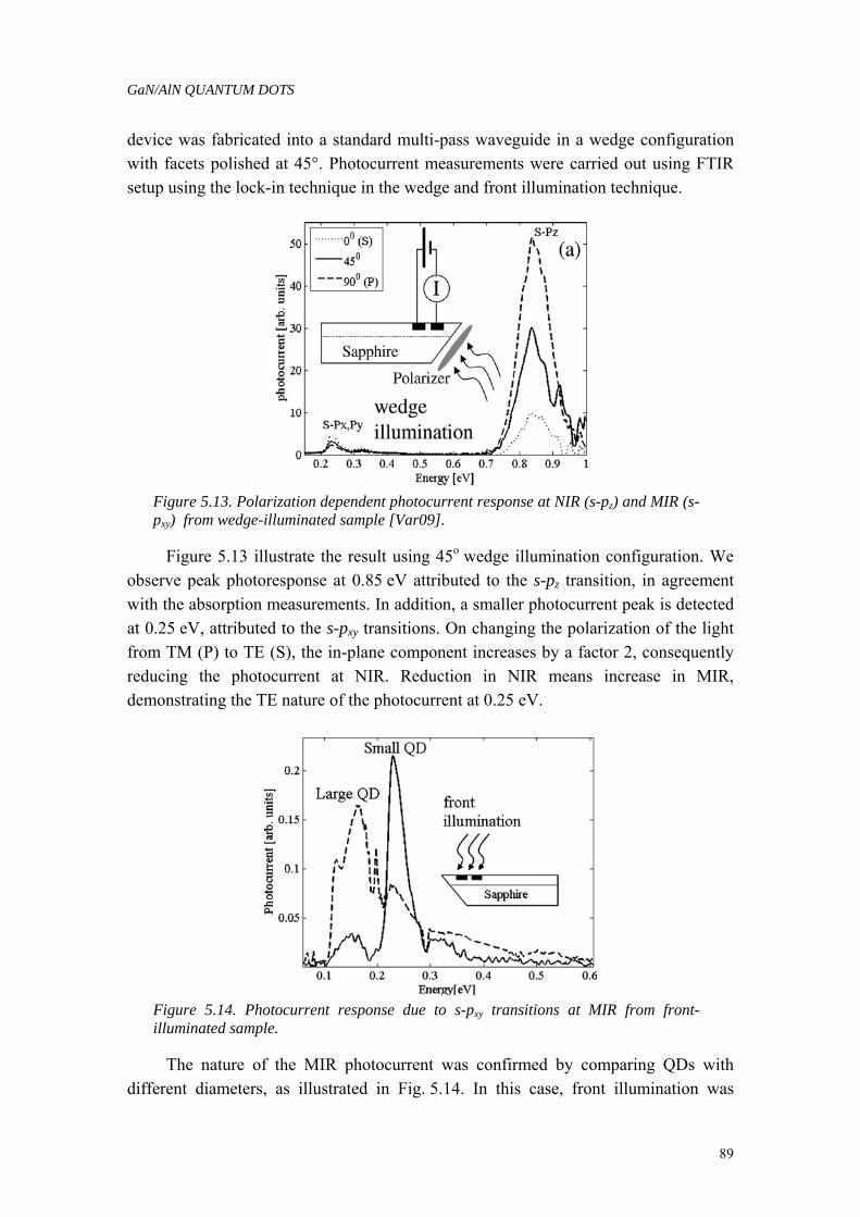
GaN/AlN QUANTUM DOTS
89
device was fabricated into a standard multi-pass waveguide in a wedge configuration with facets polished at 45°. Photocurrent measurements were carried out using FTIR setup using the lock-in technique in the wedge and front illumination technique.
Figure 5.13. Polarization dependent photocurrent response at NIR (s-pz) and MIR (s-pxy) from wedge-illuminated sample [Var09].
Figure 5.13 illustrate the result using 45o wedge illumination configuration. We observe peak photoresponse at 0.85 eV attributed to the s-pz transition, in agreement with the absorption measurements. In addition, a smaller photocurrent peak is detected at 0.25 eV, attributed to the s-pxy transitions. On changing the polarization of the light from TM (P) to TE (S), the in-plane component increases by a factor 2, consequently reducing the photocurrent at NIR. Reduction in NIR means increase in MIR, demonstrating the TE nature of the photocurrent at 0.25 eV.
Figure 5.14. Photocurrent response due to s-pxy transitions at MIR from front-illuminated sample.
The nature of the MIR photocurrent was confirmed by comparing QDs with different diameters, as illustrated in Fig. 5.14. In this case, front illumination was
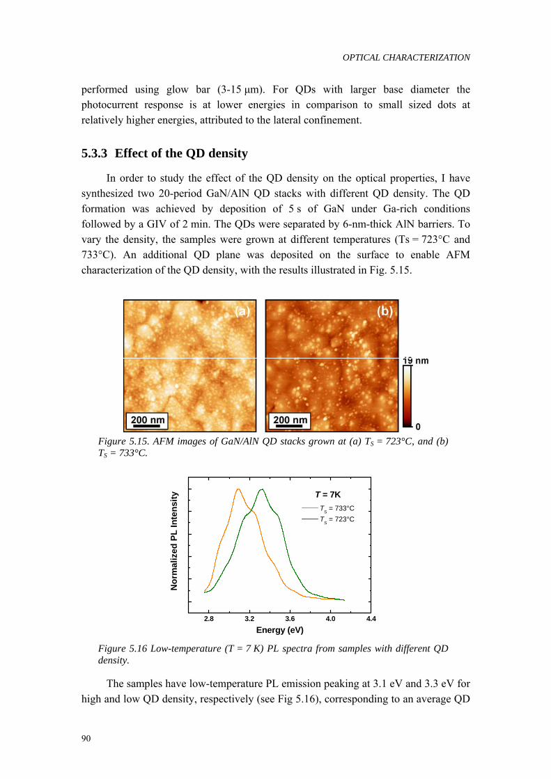
OPTICAL CHARACTERIZATION
90
performed using glow bar (3-15 µm). For QDs with larger base diameter the photocurrent response is at lower energies in comparison to small sized dots at relatively higher energies, attributed to the lateral confinement.
5.3.3 Effect of the QD density
In order to study the effect of the QD density on the optical properties, I have synthesized two 20-period GaN/AlN QD stacks with different QD density. The QD formation was achieved by deposition of 5 s of GaN under Ga-rich conditions followed by a GIV of 2 min. The QDs were separated by 6-nm-thick AlN barriers. To vary the density, the samples were grown at different temperatures (Ts = 723°C and 733°C). An additional QD plane was deposited on the surface to enable AFM characterization of the QD density, with the results illustrated in Fig. 5.15.
Figure 5.15. AFM images of GaN/AlN QD stacks grown at (a) TS = 723°C, and (b) TS = 733°C.
2.8 3.2 3.6 4.0 4.4
TS = 733°C TS = 723°C
Nor
mal
ized
PL
Inte
nsity
Energy (eV)
T = 7K
Figure 5.16 Low-temperature (T = 7 K) PL spectra from samples with different QD density.
The samples have low-temperature PL emission peaking at 3.1 eV and 3.3 eV for high and low QD density, respectively (see Fig 5.16), corresponding to an average QD

GaN/AlN QUANTUM DOTS
91
height of 1.5-2 nm on the wetting layer, in agreement with the AFM characterization. Temperature-dependent PL performed in these samples and summarized in Fig. 5.17 does not show any significant change, in spite of the different QD density.
10 1000.2
0.4
0.6
0.8
1
1.21.4
TS = 733°C TS = 723°C
Nor
mal
ized
PL
Inte
nsity
1000 / T (K-1) Figure 5.17. Thermal quenching of the PL from samples with different QD density.
These samples with different QD density were applied to the study of the lateral transport mechanisms in GaN\AlN QD heterostructures, both in the dark and under IR excitation. Standard techniques were used to define an interdigitated contact structure in which the metallization fingers fill the trench down to the AlN buffer. Electrical characterization and photocurrent experiments were performed at Technion (Israel), under the supervision of Prof. G. Bahir [Var09].
Due to the large band gap and the strong carrier confinement resulting from the large band offset between GaN and AlN, the dark current due to thermionic or field emission processes should be negligible. However, devices present a significant dark current which increases with QD density (see Fig.5.18), and monotonically decreases with decreasing temperature. This result is attributed to hopping conductivity due to inter-QD tunneling in high QD density structures. Indeed, self-assembled QDs, as a typical localized-state system, is expected to show hopping transport, as demonstrated in Si\Ge [Yak99] and InGaAs\GaAs QDs [Son01].

OPTICAL CHARACTERIZATION
92
0 1 2 3 4 5
10-3
10-2
10-1
Cur
rent
(µA
)
Voltage (V)
High density Low density Reference
Figure 5.18. Room-temperature dark current for samples with different QDs densities. The reference sample contains no QDs.
The dark conductance of the two samples with different QD density at low bias is presented as a function of temperature in fig. 5.19. At higher temperatures, the conductance follows an activation behavior characteristic of nearest-neighbor hopping (NNH). Below ~ 160 K, the temperature dependence becomes weaker, as carriers may optimize their paths via variable-range hopping (VRH). In that regime, the
conductance follows ( )1/ 30 /T Te− , indicating that the transport follows the 2D Mott-VRH.
In the NNH regime the activation energy is inversely proportional to the inter-dot distance while in the VRH regime the activation (in T-1/3 scale) is inversely proportional to the QD dimensions. These results are consistent with structural characterization obtained by AFM [Var09]. Below 50K, the conductance behavior depends both on temperature and electric field (F), resulting in a deviation from the
1/3T − dependence.
Figure 5.19. Dark conductance vs. 1/kT for samples with high and low QD density. Inset: Conductance vs. 1/T1/3 for both samples. (After [Var09]).

GaN/AlN QUANTUM DOTS
93
5.4 Conclusions
In conclusion, I have achieved the growth of QDs with the required size distribution for observation of intraband absorption at the technologically important telecom wavelengths. Although the size of the nanostructures required at this wavelength had been achieved before by N-rich growth conditions, but the control of density was difficult due to the reduced mobility of the adatoms under these growth conditions. In contrast, I have demonstrated that Ga-rich conditions provide an extra advantage in terms of QD dilution.
Optical studies on the SLs of QDs reveal suppression of nonradiative recombination even at room temperature, due to the large lateral confinement caused by the huge GaN/AlN conduction band offset. Intraband characterization of the samples shows strong TM-polarized absorption in the NIR region, signaling s-pz transition, and MIR s-pxy absorption for front illumination. Though the QD density does not have significant influence on the thermal quenching of luminescence, the density does affect the performance of lateral QDIPs: high QD density results in an enhancement of the dark current due to nearest-neighbor hopping transport.

CONCLUSIONS
94

Chapter 6
GaN/AlGaN quantum wells
In this chapter I show how the intersubband (ISB) transitions can be tuned from near-infrared to mid-infrared wavelengths by engineering the quantum confinement and electric field in the heterostructures. Optical characterization methods like photoluminescence and ISB absorption measurements are used to probe the effects of confinement, electric-field and carrier concentration on the transition energy. The experimental measurements are supported by simulations using the Nextnano3 Schrödinger-Poisson solver. Discussion on many-body-effects encountered in III-N materials is presented.
6.1 Introduction
The optoelectronic potential of III-nitride intersubband (ISB) optoelectronics does not stop in the near-infrared (NIR). The large conduction band offset, used to observe ISB transitions at 1.55 µm, can also be reduced to push the transition wavelength into mid- and far-infrared (MIR, FIR) spectral regions, even up to the Terahertz domain. The MIR spectral region is unique for applications especially in the atmospheric transparency window, which allows us to see distant objects without the influence of chemical elements in the air. Lasers and detectors operating in the transparency window of the atmosphere are excellent tools for remote sensing. The MIR also plays a significant role in medical diagnostics, as complex molecules like glucose have their fundamental vibrational modes in this spectral region. In addition, high power MIR lasers can be used for surgical purposes. The potentially important technological applications in FIR region have pushed extensive efforts to develop optoelectronics components. A promising approach consists of unipolar devices relying on ISB transitions in GaAs/AlGaAs. However, As-based materials require cryogenic operating temperatures due to an intrinsic material limitation: the low LO-phonon energy, below the room-temperature thermal energy.
From the schematic spectral diagram in Fig. 6.1 we can make out the ISB transition ranges covered by III-As and III-N materials. Some regions of the spectrum are inaccessible by III-As and III-N materials due to Restrahlen absorption bands: the absorption band for GaN falls between hωTO = 67.6 meV (~ 18 µm) and hωLO = 92 meV (~ 13.5 µm).

INTRODUCTION
96
Restrahlen band
Figure 6.1. Material systems covering various spectral regions
The main advantages of the GaN/AlGaN system for FIR ISB optoelectronics stem from the large LO-phonon energy of 92 meV. High magnitude of LO-phonon energy reduces thermal back filling of carriers into the lower laser state for energies greater than room temperature thermal energy kT ~ 25 meV, and also indirectly increases the lifetime of the upper lasing state by reducing the relaxation of electrons with higher in-plane kinetic energy. Secondly, very strong electron-LO phonon interaction results in ultrafast carrier relaxation, allowing rapid depopulation of the ground state. Owing to these advantages, a number of theoretical proposals for GaN/AlGaN Terahertz quantum cascade lasers have been reported [Enr09, Vuc05, Gre04, Sun05].
Although lot of progress has been made by simulations, experimental proof of ISB transitions for long wavelengths is still lagging behind. There are reports of MIR absorption in the range between 2-4 µm from AlInN/GaN superlattices (SLs) [Nic05, Mal09] and up to 5.3 µm using GaN/AlGaN [Per09]. The extension of the nitride ISB technology towards longer wavelengths sets new material and design challenges: the GaN/AlN technology was developed on sapphire templates, and is therefore limited by the sapphire infrared (IR) absorption cutoff at ~ 5 µm. ISB transitions can be pushed to lower energies by changing the design of the heterostructures, while growing on IR-transparent substrate, such as semi-insulating Si(111). In this chapter we will show how the GaN/AlGaN ISB wavelength can be tuned from NIR up to 10 µm wavelength by engineering the quantum confinement and electric field in the heterostructures.
6.2 Calculation of the electronic structure
The design of the GaN/AlGaN SLs for longer wavelengths was performed using the Nextnano3 8×8 k.p Schrödinger-Poisson solver with the material parameters described in Chapter 4. The target was to reduce the energy difference between the two first electronic levels, e2-e1, while keeping at least 2 levels localized in the quantum

GaN/AlGaN QUANTUM WELLS
97
well (QW) to observe only bound-to-bound transitions. Reducing the e1 and e2 separation implies decreasing the quantum confinement and/or reducing the polarization-induced internal electric field. Therefore, it can be achieved by decrease of the Al mole fraction in the barrier, increase of the QW width or decrease of the barrier width. Figure 6.2 shows the calculated evolution of the electronic levels for GaN/AlGaN (5 nm / 3 nm) SLs with varying Al mole fraction in the barrier.
Figure 6.2. Variation of the conduction band diagram when varying the Al mole
fraction in the barrier of GaN/AlGaN (5 nm / 3 nm). The Al in the barriers is 35%, 30% and 20%.
6.3 Growth and structural characterization
The GaN/AlGaN structures were grown by plasma-assisted molecular beam epitaxy (PAMBE) on commercially-available GaN-on-sapphire templates1, and on a commercial crack-free GaN high electron mobility transistor (HEMT) structure grown on Si(111) (referred hereafter as GaN-on-Si(111) template)2. The substrate temperature was set at 700oC, about 20oC below the standard Ga desorption temperature used for GaN/AlN structures [Kan08], which reduces the probability of interdiffusion of GaN and AlGaN. Both the QW and the barrier were grown under Ga-rich conditions. The barrier Al content was deduced from reflection high-energy electron diffraction (RHEED) intensity oscillations during the growth of AlN under Al-limited conditions. The SL structure consists of 40 periods of AlGaN/GaN sandwiched between bottom and top AlGaN cladding layers. In section 4.5.2 c) of this thesis, we showed the influence of capping layers on the magnitude of ISB absorption due to the polarization-induced band bending. Thus, the composition of AlGaN cap layer was chosen carefully to homogenously distribute the carriers in the SL.
1 Supplier: Lumilog 2 Supplier: DOWA Electronics Materials, Inc.

GROWTH AND STRUCTURAL CHARACTERIZATION
98
To observe the ISB absorption in the MIR, it is required to grow the structure on a transparent substrate. Figure 6.3 shows the absorption spectrum of sapphire compared to that of the GaN-on-Si(111) templates used for our study. The sapphire present a sharp spectral cutoff at ~ 5 µm, whereas GaN-on-Si(111) remains transparent up to ~ 14 µm. The absorption band between 13-18 µm is attributed to the Restrahlen absorption of the GaN HEMT structure.
1 10 100
0
20
40
60
80
100
Tran
smita
nce
(%)
Wavelength (µm)
Sapphire HEMT on Si (111)
Figure 6.3. Transmission spectra of a sapphire substrate compared to a commercial GaN HEMT structure on semi-insulating Si(111).
The AFM image in Fig. 6.4 compares the surface morphology of the GaN-on-Si(111) template and a GaN/AlGaN SL grown on top. Both structures present atomic terraces, resulting from step-flow growth mode, and a comparable root-mean-square (rms) surface roughness. The substrate presents pits (black spots in the figure) corresponding to the surface termination of edge-type threading dislocations, with a density of ~ 3×109 cm-2. In the case of the SL, the surface presents the spiral hillocks characteristic of plasma-assisted molecular beam eptitaxy (PAMBE), indicating a density of screw dislocations in the order of ~ 109 cm-2. These defect densities are standard for samples grown on Si(111). A very important feature is the crack-free nature of the samples with Al mole fraction below 0.35.
Figure 6.4. Atomic force microscopy images of the GaN-on-Si(111) template and of GaN/Al0.1Ga0.9N (7 nm / 4 nm) SL grown on top.
SL
300 nm
Substrate
300 nm

GaN/AlGaN QUANTUM WELLS
99
The structural quality of the sample was further characterized using transmission electron microscopy (TEM), as illustrated in Fig. 6.5 for a SL consisting of 40 periods of GaN / Al0.2Ga0.8N (4 nm / 7 nm). We observe uniform layer thickness with sharp interfaces. X-ray diffraction measurements reveal a full width at half maximum (FWHM) of 600 arcsec for the ω-scan of the (0002) SL reflection.
Figure 6.5. (a) Cross-section TEM image of the Si-doped GaN/Al0.1Ga0.9N (7 nm / 4 nm) SL structure grown on GaN-on-Si(111). (b) High-resolution TEM image illustrating three periods of the SL and (c) corresponding profile of one period of the SL where the Al0.1Ga0.9N is well distinguished.(TEM images by Dr. E. Sarigianidou, INPG)
6.4 Optical characterization
Figure 6.6 displays typical low-temperature (T = 10 K) photoluminescence (PL) spectra comparing 5 nm / 3 nm GaN/AlGaN SLs with the Al content in the barrier varying from 0.2 to 0.35 and grown simultaneously on GaN-on-sapphire and GaN-on-Si(111) templates. Whatever the substrate, the structures present comparable optical quality, with a spectral red shift for samples grown on GaN-on-Si(111) due to the different strain state. Reducing the barrier Al mole fraction results in a blue shift of the PL due to reduction of internal electric field. Whatever the substrate, the structures present comparable line width.

OPTICAL CHARACTERIZATION
100
Figure 6.6. Low-temperature (T = 10 K) PL spectra from GaN/AlxGa1-xN SLs grown on GaN-on-sapphire or GaN-on-Si(111) templates. The oscillations superimposed to the PL peaks are due to Fabry-Perot interference.
Figure 6.7. (a) Infrared absorption spectra for TM-polarized light measured in GaN/AlGaN SLs with different barrier Al contents and QW widths, grown either on sapphire or on Si(111) templates. (b) Relative spectral width as a function of the absorption peak wavelength for SL grown on different substrates. Dashed line forms eye-guide.
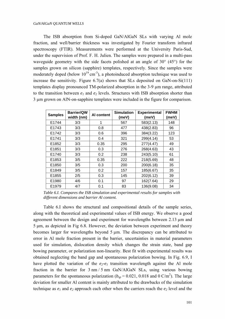
GaN/AlGaN QUANTUM WELLS
101
The ISB absorption from Si-doped GaN/AlGaN SLs with varying Al mole fraction, and well/barrier thickness was investigated by Fourier transform infrared spectroscopy (FTIR). Measurements were performed at the University Paris-Sud, under the supervision of Prof. F. H. Julien. The samples were prepared in a multi-pass waveguide geometry with the side facets polished at an angle of 30° (45°) for the samples grown on silicon (sapphire) templates, respectively. Since the samples were moderately doped (below 1019 cm-3), a photoinduced absorption technique was used to increase the sensitivity. Figure 6.7(a) shows that SLs deposited on GaN-on-Si(111) templates display pronounced TM-polarized absorption in the 3-9 µm range, attributed to the transition between e1 and e2 levels. Structures with ISB absorption shorter than 3 µm grown on AlN-on-sapphire templates were included in the figure for comparison.
Samples Barrier/QW width (nm) Al content Simulation
(meV) Experimental
(meV) FWHM (meV)
E1744 3/3 1 567 583(2.13) 148 E1743 3/3 0.8 477 438(2.83) 96 E1742 3/3 0.6 396 384(3.22) 123 E1741 3/3 0.4 321 299(4.14) 53 E1852 3/3 0.35 295 277(4.47) 49 E1851 3/3 0.3 276 268(4.63) 43 E1740 3/3 0.2 238 243(5.10) 61 E1853 3/5 0.35 222 218(5.69) 48 E1850 3/5 0.3 200 200(6.18) 35 E1849 3/5 0.2 157 185(6.67) 35 E1855 2/5 0.3 145 202(6.12) 39 E1980 4/6 0.1 97 162(7.64) 29 E1979 4/7 0.1 83 136(9.08) 34
Table 6.I. Compares the ISB simulation and experimental results for samples with different dimensions and barrier Al content.
Table 6.I shows the structural and compositional details of the sample series, along with the theoretical and experimental values of ISB energy. We observe a good agreement between the design and experiment for wavelengths between 2.13 µm and 5 µm, as depicted in Fig 6.8. However, the deviation between experiment and theory becomes larger for wavelengths beyond 5 µm. The discrepancy can be attributed to error in Al mole fraction present in the barrier, uncertainties in material parameters used for simulation, dislocation density which changes the strain state, band gap bowing parameter, or polarization non-linearity. Best fit with experimental results was obtained neglecting the band gap and spontaneous polarization bowing. In Fig. 6.9, I have plotted the variation of the e2-e1 transition wavelength against the Al mole fraction in the barrier for 3 nm / 5 nm GaN/AlGaN SLs, using various bowing parameters for the spontaneous polarization (bsp = 0.021, 0.018 and 0 C/m2). The large deviation for smaller Al content is mainly attributed to the drawbacks of the simulation technique as e1 and e2 approach each other when the carriers reach the e2 level and the

OPTICAL CHARACTERIZATION
102
possibility of many-body effects. From our simulations no clear conclusion on effect of bsp could be extracted, but it is still necessary to quantify the role of bowing at longer wavelengths.
20 40 60 80 100
2.0
2.5
3.0
3.5
4.0
4.5
5.0
5.5
e 2-e1 (µ
m)
Al mole fraction (%)
Experiment Simulation
GaN / AlGaN (3 nm / 3 nm)
Figure 6.8. Comparison of theoretical and experimental data for samples with absorption between 2-5 µm at bsp = 0 C/m2.
20 24 28 32 36
5.0
5.5
6.0
6.5
7.0
7.5
8.0
e 2-e1 (
µm)
Al mole fraction
Experiment bsp = 0.021 C/m2
bsp = 0.018 C/m2
bsp = 0 C/m2
GaN/AlGaN 5 nm / 3 nm
n = 1x1019 cm-3
Figure 6.9. Evolution of ISB transition energy for various spontaneous bowing parameters of 0, 0.018 and 0.021 C/m2 [Amb01].
The relative spectral width ∆λ/λ of the ISB absorption, represented in Fig. 6.7(b) versus wavelength, remains around 20% in the whole MIR range –to be compared with typical values of 10-15% for As-based structures in the same spectral range, and with 10-20% for GaN/AlN QWs in the near-infrared range. The line broadening can be attributed to thickness fluctuations and alloy inhomogeneities, whose effect is magnified by the polarization-induced electric field in nitride materials. Additionally, the polarization-induced band bending may lead to inhomogeneous carrier screening of the internal electric field in the QWs, and hence a broadening of the absorption lines. This effect is generally negligible for AlN/GaN SLs as the huge internal electric field cannot be easily screened, and few wells are affected by the polarization-induced band

GaN/AlGaN QUANTUM WELLS
103
bending (see Fig. 4.21). However, in the case of low Al content structures the smaller electric field is easily screened, as described above, and the polarization-induced band bending varies slowly extending over a number of wells, inducing a carrier gradient, and ultimately leading to optical broadening. In the 2-4 µm range, GaN/AlGaN SLs present an abnormally broad spectral width independently of the substrate, either GaN-on-sapphire or GaN-on-Si(111). This is attributed to crack development in those structures.
6.5 Effect of doping
To observe direct absorption, the structures must be heavily doped. Typical doping concentrations for direct absorption in AlN/GaN SLs are in the range of 1019 cm-3 [Iiz00]. Carrier confinement at higher doping levels results in significant many-body effects, which shift the ISB energy levels [Hel03]. Therefore, the study of doping is important to understand the absorption mechanisms and introduce the adequate correction in the device design.
To probe these effects, I grew two series of samples, one with 3 nm / 3 nm GaN/Al0.2Ga0.8N QWs with Al0.1Ga0.9N cladding layers (A series), and another one with 7 nm / 4 nm GaN/Al0.1Ga0.9N QWs with Al0.03Ga0.97N cladding layers (B series). The structures were designed so that calculations using the Nextnano3 8-band k.p Schrödinger-Poisson solver predict two electronic levels confined in the QWs with expected ISB absorption at ~ 5.0 µm (A series) and ~ 11 µm (B series) for a doping level n = 1 × 1017 cm-3, as illustrated in Fig. 6.10. In each series, the QWs were doped with Si concentrations varying between n = 1 × 1019 cm-3 and n = 1 × 1021 cm-3. Reference samples with identical structure were simultaneously grown on 4-µm-thick GaN-on-sapphire templates.
12 16 20 248 10 12 14-0.2
-0.1
0.0
0.1
0.2
0.3
0.4
0.5
Depth (nm)
e2
(b)
Ener
gy (e
V)
Depth (nm)
(a)
e1
Figure 6.10. Band diagram of (a) GaN/Al0.2Ga0.8N (3 nm / 3 nm) SLs and (b) GaN/Al0.1Ga0.9N (7 nm / 4 nm) SLs. The e2-e1 difference is estimated at (a) 0.246 eV (= 5.0 µm) and (b) 0.106 eV (= 11 µm) for a doping level n = 1×1017 cm-3.

EFFECT OF DOPING
104
Figure 6.11 displays the low temperature (T = 7 K) PL spectra from series A and B measured with a continuous-wave frequency-doubled Ar laser (λ = 244 nm) focused on a 50 µm spot, and analyzed by a 0.46 m focal length spectrometer equipped with a charge-coupled device (CCD) camera. The lines at 339 nm and 349 nm from series A and B, respectively, are assigned to the band-edge emission from the top AlGaN cladding layer. The SL luminescence peaks at (a) 353 nm and (b) 358 nm for a doping level n = 1019 cm-3, and blue shifts by more than 5 nm when increasing the doping level to n = 1020 cm-3. The magnitude of this shift cannot be explained only by the screening of the polarization-induced internal electric field in the QWs. In addition, the luminescence broadens and is strongly quenched for n ≥ 1 × 1020 cm-3. This behavior is attributed to band filling, as depicted in the schematic representation of the band edge in Fig. 6.12. The Fermi level gets deep into the conduction band, and thus we observe momentum non-conserving transitions at higher energies than the band gap. This interpretation is consistent with the observed blue shift, the PL quenching at high doping levels and the broadening and asymmetry of the PL peaks.
335 340 345 350 355 360 365
GaN
SL
Nor
mal
ized
PL
inte
nsity
Wavelength (nm)
AlGaN (a)n = 1020 cm-3
n = 5×1019 cm-3
n = 1019 cm-3
T = 7 K
345 350 355 360 365 370
GaN
SL
Nor
mal
ized
PL
inte
nsity
Wavelength (nm)
AlGaN (b)
n = 1020 cm-3
n = 2×1020 cm-3
n = 5×1019 cm-3
n = 1019 cm-3
T = 7 K
Figure 6.11. Low-temperature (T = 7 K) PL spectra from (a) GaN/Al0.2Ga0.8N (3 nm / 3 nm) and (b) GaN/Al0.1Ga0.9N (7 nm / 4 nm) grown on GaN-on-sapphire with different doping levels. Spectra are vertically shifted for clarity. Dashed lines are eye-guides to indicate the position of the PL emission assigned to the top AlGaN cladding and to the SL.

GaN/AlGaN QUANTUM WELLS
105
Figure 6.12 Band diagram depicting the bandfilling effect.
This trend is consistent with the effect of doping on bulk GaN [Yos99, Bin99]. For GaN layers doped in the <1019 cm-3 range, the emission first shifts to longer wavelengths, which is attributed to band renormalization due to Coulomb effects. In GaN/AlGaN QWs, these effects are negligible in comparison to the blue shift induced by screening of the polarization induced internal electric field. For n > 1019 cm-3, bulk GaN enters the band filling regime, hence shifting to higher energies.
1 0.5
1 2 3 4 5 6 7
0.2
n = 5×1020 cm-3
n = 1020 cm-3
Nor
mal
ized
abs
orpt
ion
Wavelength (µm)
n = 5×1019 cm-3
(a)0.3
Energy (eV)0.6 0.4 0.2
2 4 6 8 10
n = 2×1020 cm-3
n = 5×1020 cm-3
n = 1020 cm-3
Nor
mal
ized
abs
orpt
ion
Wavelength (µm)
n = 5×1019 cm-3
(b)
Energy (eV)
Figure 6.13. Infrared absorption spectra for TM-polarized light measured from (a) GaN/Al0.2Ga0.8N (3 nm / 3 nm) and (b) GaN/Al0.1Ga0.9N (7 nm / 4 nm) quantum wells grown on GaN-on-Si(111) with different doping levels. Spectra are vertically shifted for clarity.
Broadening Band filling (blue shift)
EF

EFFECT OF DOPING
106
The ISB absorption was investigated at room temperature using FTIR in samples prepared in multipass waveguide geometry with 30° facets. The ISB absorption measurements carried out on series A and B are depicted in Figs. 6.13(a) and (b), respectively. The TM-polarized absorption peaks shift systematically towards higher energies with doping, in contradiction to simulations considering the screening of the polarization-induced internal electric field [Kan09]. The discrepancy between simulations and experiments is attributed to many-body effects, such as exchange interaction, depolarization shift and Coulomb interaction.
In order to understand the results of this experiment, and the discrepancy with simulations we should take into account the various factors that can shift the transition energy as a function of doping, particularly the screening of the polarization-induced internal electric field and many-body effect such as the exchange interaction, Coulomb interaction and depolarization shift.
In the case of GaN/AlGaN, the internal electric field decreases for decreasing Al mole fraction in the barrier, so that lower doping concentrations are required to screen effectively the electric field. The screening pushes up the ground electronic level e1, and the magnitude of the shift increases if e1 is located within the triangular region of the QW. Thus the overall influence of screening, illustrated in Fig. 6.14, translates into a reduction of the e2-e1 energy difference.
Figure 6.14. Influence of doping on e1 and e2 separation due to the screening of the internal electric field: (a) n = 1017 cm-3, and (b) n = 1019 cm-3.
Our simulating tool, Nextnano3, incorporates the effects of electric field screening. However, we have observed that the quantum calculations present convergence problems when dealing with highly degenerate semiconductors. In order to force the convergence of the calculation in a reasonable time, we have opted for making first a classical calculation of the band diagram and Fermi level, followed by a quantum calculation of the confined energy levels using the k.p method. This approach provided a more reliable description of the band diagram, but the position of the Fermi level is significantly under estimated. Apart from the effect of carrier screening, the

GaN/AlGaN QUANTUM WELLS
107
magnitude of many-body effects could not be simulated by the Nextnano3 tool since it accounts only for Hartree potential solution of the self-consistent Schrodinger-Poisson equation, however to include many-body effects, one must solve the Hartree-Fock equation.
The many-body effects can be classified in two groups: affecting the energy levels (exchange interaction) and affecting the absorption frequency (depolarization shift and Coulomb interaction). The corrections for all these three terms are explained in [Blo89, Guo09] under local density approximation (LDA), and solutions to the exchange interaction in QWs are dealt by Bandara et. al [Ban88].
We have previously shown that the dominant many-body effect in the case of GaN/AlN QWs is the exchange interaction [Tch06]. This interaction stems from Pauli’s principle: the repulsion among electrons with the same spin can lower the energy of the subbands that are heavily populated. In this case, the density of states (DOS) is expected to play a major role in fixing the transition energy [Ban88]. In our case of samples, the smaller energy shift with doping in series B might be a consequence of the energy levels being relatively deconfined in comparison to series A, thus B has lower DOS. However, we should notice that the high doping levels used in this study should push the Fermi level beyond the second electronic level. The resulting down shift of e2 should partially compensate the effect of exchange on the transition energy.
In addition to the exchange effect, the depolarization (plasmonic) shift also influences transition energy levels depending on the carrier density. When the carrier density in the QW increases, the ISB absorption cannot be considered as a single particle transition. The photon induces a collective excitation of the electron plasma in the ground level. This collective carrier oscillation induces a blue shift of the ISB transitions, which is directly proportional to n2D/e2-e1, n2D being the effective 2D electron density. Plasmonic effects are quite low at shorter wavelengths but as e1 and e2 approach the plasmonic effect becomes comparable with the exchange term, both inducing a blue shift of the ISB transition.
Coulomb (excitonic) effects are due to the interaction between an excited electron and the hole that it left in the ground state. This effect decreases the ISB transition energy, working against exchange and depolarization shift [Blo89].
The influence of these many-body effects shown in Fig. 6.15 has been investigated by Helman et al. for GaN/AlN structures [Hel03], treating the various many-body-effects as just perturbations when the influence of electric-field screening is very small.

EFFECT OF DOPING
108
Figure 6.15. Calculated ISB energy of GaN/AlN QWs vs well thickness for different doping concentrations (solid line: 1017 cm-3, dashed line: 1019 cm-3, and dotted line: 2 × 1019 cm-3). In the inset:iIndividual influences of exchange (dotted line), depolarization-shift (dash-dot line) and Coulomb interaction (dashed line), and resultant energy shift (solid line) (After [Hel03]).
In the GaN/AlGaN SLs described in this chapter, the shift related to many-body effects should be due to the combination of exchange interaction and depolarization shift. Unfortunately, the magnitude of the shift induced by many-body effects is comparable to the value of e2-e1, so that the approximations that consider exchange interaction as a perturbation of the Hartree-Fock equation are no longer valid, and new models must be developed to describe this effect.
6.6 Conclusions
In conclusion, we have observed ISB absorption in the MIR spectral region using Si-doped GaN/AlGaN SLs grown on semi-insulating GaN-on-Si(111) templates. The TM-polarized ISB absorption shows a systematic red shift for decreasing Al mole fraction in the barriers and increasing well width, in agreement with simulations of the electronic structure. The ISB relative spectral width remains around 20% in the whole MIR range.
In addition, doping is identified as a critical parameter to reach the targeted operating wavelength. For increasing doping levels, we observe a large broadening of the ISB absorption linewidth accompanied by a significant blue shift, which is attributed to many-body effects. This result is supported by photoluminescence spectra showing significant broadening and blue shift as a result of band filling in the QW. The magnitude of the ISB energy shift due to many-body effects is comparable to the predicted e1-e2 transition, so that it cannot be treated as a perturbation. With the presented evidence, many-body effects become a critical parameter for design of nitride-based ISB structures operating at longer wavelengths, and all the theoretical calculations of devices for the far infrared should be accordingly revised.

109
Chapter 7
Conclusions and perspectives
7.1 Conclusions
The aim of this work was two-fold: first, to improve the performance and the understanding of the material issues involved in the GaN/AlN intersubband (ISB) technology, targeting operation in the near-infrared (NIR), and particularly at 1.55 µm. Secondly, to develop heterostructures with ISB wavelength covering the whole mid-infrared (MIR) spectral region, as a first attempt to push the operation of nitride-based ISB devices towards longer wavelengths. The achievements in these fields are detailed below.
I have first studied the effect of plasma-assisted molecular beam epitaxy (PAMBE) growth and design parameters on the performance of Si-doped GaN/AlN quantum well (QW) superlattices (SLs) for ISB optoelectronics in the NIR spectral region. The Nextnano3 8-band k.p Schrodinger-Poisson solver was adapted to the design of GaN/AlN NIR ISB structures. Then, in order to optimize the growth parameters, I have analyzed systematically the misfit relaxation mechanisms. The use of a Ga excess during the growth of both GaN and AlN was found to play a crucial role in the relaxation process, reducing plastic relaxation and preventing cracks. The large misfit stress between the substrate and the SL is relaxed mostly by generation of edge-type threading dislocations. The final strain state of the superlattice, reached after 10-20 periods, is independent of the substrate (either GaN or AlN templates), which is reflected as substrate independent (GaN, AlN or AlGaN) ISB absorption energy.
Once the influence of the substrate becomes negligible, we observe a periodic partial relaxation of quantum wells and barriers. This phenomenon can be related to the presence of stacking faults that originate when starting the AlN deposition and close after deposition of the barrier forming loops with an in-plane length of tens of nanometers. However, the presence of staking faults is predicted not to cast much influence on the ISB transition energy, as their effect is within the broadening limit. The ISB absorption from these structures shows a good fit with the theoretical calculations, thus reliable simulations of complex designs can be performed.
Finally, I have studied the effect of the polarization-induced internal electric field on the ISB absorption. The polarization discontinuity due to the cap layer can induce

CONCLUSIONS
110
the population or depletion of active QWs. The influence of capping layer on ISB absorption magnitude presented in this chapter has its implications on the design of waveguides and contact region for the complex structures. On the other hand, the reduction of the internal electric field results in red shift of the ISB transitions with respect to polar material. The experimental results in the semipolar GaN/AlN SLs are consistent with simulations of the electronic structure, which predict a reduction of the polarization-induced internal electric field by more than one order of magnitude.
The synthesis of GaN/AlN quantum dot (QD) structures for NIR ISB optoelectronics has also been addressed. Intraband absorption at NIR requires QDs with a height around 1-1.5 nm. Growth of QDs with the required size was achieved under N-rich and Ga-rich growth conditions. Due to enhanced adatom mobility, Ga-rich growth conditions favour a reduction in density of QDs in comparison to N-rich conditions. Optical studies show suppression non-radiative processes even up to room temperature. Intraband characterization of the samples shows strong TM-polarized absorption in the NIR region, signaling s-pz transition, and MIR s-pxy absorption for front illumination. Though the QD density does not have significant influence on the thermal quenching of luminescence, the density does affect the performance of lateral QD infrared photodetectors: high QD density results in an enhancement of the dark current due to nearest-neighbor hopping transport.
The III-N ISB technology in the NIR region takes advantage of the sapphire substrate transparency. However, the extension towards longer wavelengths is blocked by the sapphire absorption cutoff beginning at ~ 5µm. To surmount this problem we have grown GaN/AlGaN structures on semi-insulating GaN-on-Si(111) templates, without compromising the structural and optical quality. The TM-polarized ISB absorption shows a systematic red shift for decreasing Al mole fraction in the barriers and increasing well width, in agreement with simulations of the electronic structure. The ISB relative spectral width remains around 20% in the whole MIR range up to ≈ 10 µm. But the important direct absorption criterion is satisfied only at very high doping concentrations of 1 × 1019 cm-3.
The ISB absorption shows high sensitivity to doping, which is also identified to be the critical parameter to reach the targeted operating wavelength. For increasing doping levels, we observe a large broadening of the ISB absorption line width accompanied by a significant blue shift, which is attributed to many-body effects. This result is supported by photoluminescence spectra showing significant broadening and blue shift as a result of band filling in the QW. The magnitude of the ISB energy shift due to many-body effects is comparable to the predicted e1-e2 transition, so that it cannot be treated as a perturbation. With the presented evidence, many-body effects become a critical parameter for design of nitride-based ISB structures operating at longer wavelengths, and all the theoretical calculations of devices for the far infrared should be accordingly revised.

CONCLUSIONS AND PERSPECTIVES
111
7.2 Perspectives
The domain of III-N ISB devices has seen several important milestones in the past years, as, for example, the first prototypes of quantum cascade detectors and electro-optical modulators, and the first observation of ISB emission from GaN/AlN quantum wells and quantum dots. Although in-depth understanding of the polarization-induced electric field in III-N heterostructures has allowed the design and fabrication of devices based on cascade structures, a basic requirement like clear observation and control of resonant tunneling transport still remains a challenge. Resonant transport measurements will help us to understand the behavior of energy levels under the influence of applied bias, which will ultimately aid in the design of device structures with relatively accurately placed energy levels. This is yet to be reality probably due to the high dislocation density and the high electric fields within the materials. Important aspects such as coupling between QWs need to be improved, since it dictates the carrier scattering processes, influencing gain
ISB light emission at NIR wavelengths has been detected from GaN/AlN quantum wells and quantum dots. However, it is necessary to attain a good understanding of the carrier scattering mechanisms, so that we can modify the design to tune the carrier lifetime and achieve lasing. The energy levels placed at LO-phonon resonance promotes rapid removal of electrons from the lower lasing state, preventing thermal backfilling. The large LO-phonon energy above room-temperature thermal energy ~ 26 meV gives extra degree of freedom to design the QC structures for operation at higher temperatures. On the contrary we need longer excited state lifetimes which is not easy to achieve due to strong electron-phonon interaction- the lifetime of the excited state can be increased by placing suitably-designed multi-quantum well barriers on either sides of the active quantum well. Other direct method would be to etch one-dimensional (1D) nanostructures to reduce the phonon channels, as proposed by Tredicucci et al. [Tre09]. Depending on the strength of carrier confinement, the lateral dimension of 1D nanostructures can be fixed. The work in this direction has already been initiated starting with pillar-based resonant tunneling diodes, basically to filter the effect of dislocations.
On the other hand, from our experiments we observe an ISB spectral width of ~ 20% in III-Ns, to be compared to ~ 10% in III-As materials. This is because we are working in the limit of huge internal electric-field of the material system, which tends to broaden the energy levels. In addition, doping induced many-body effects and band-filling also contribute to the broadening. The situation is slightly critical in comparison to other III-V systems as it might block the extension of wavelengths towards FIR. If we are limited by energy level broadening, we might have to adopt active region designs like bound-to-continuum, which allows radiative transition diagonal in real-

PERSPECTIVES
112
space. For this designs which could possibly enhance diagonal oscillator strength must be considered.
Theoretical simulation of structures at NIR shows good agreement with experimental results, whereas it becomes slightly complex as we move to longer wavelengths. The transition energy and FWHM are influenced by numerous factors like many-body effects, electric-field and alloy composition. Many-body effects induce change in energy by almost 50% of the transition energy, which is beyond the capabilities of the present models used for calculations this calls for new models for simulation of such structures.
Finally, III-N structures have reached a certain level of maturity in terms of growth for binary compound (AlN, GaN) based structures. We have managed to grow uniform layers with sharp interfaces. However, barriers with ternary compounds (AlGaN) require much more work to improve the uniformity of alloy composition and interface quality. The effect of dislocations is also critical, as they introduce thickness fluctuations and relax the structures changing the electric-field. Dislocations induce high dark currents in photocurrent detectors leading to reduced device performance. Therefore, improved material quality is a critical issue to achieve competitive device performance.

References [Ade02] C. Adelmann, N. Gogneau, E. Sarigiannidou, J.-L. Rouviere, and B. Daudin, Appl.
Phys. Lett. 81 3064 (2002)
[Ade03] C. Adelmann, E. Sarigiannidou, D. Jalabert, Y. Hori, J.-L. Rouviere, B. Daudin, S. Danget, C. Bru-Chevallier, T. Shibata, and M. Tanaka, Appl. Phys. Lett 82 4154 (2003)
[Ade03b] C. Adelmann, J. Brault, G. Mula, B. Daudin, L. Lymperakis, and J. Neugebauer, Phys. Rev. B 67, 165419 (2003)
[Aki05] R. Akimoto, B. S. Li, K. Akita, and T. Hasama, Appl. Phys. Lett. 87, 181104 (2005)
[All76] S. J. Allen, Jr., D. C. Tsui, and B. Vinter, Solid State Commun. 20, 425 (1976)
[And00] A. D. Andreev and E. P. O’Reilly, Phys. Rev. B 62, 15851 (2000)
[And01] A. D. Andreev and E. P. O’Reilly, Appl. Phys. Lett. 79, 521 (2001)
[Ama89] H. Amano, M. Kito, K. Hiramatsu, and I. Akasaki, Jpn. J. Appl. Phys. 28, L2112 (1989).
[Amb00] O. Ambacher, B. Foutz, J. Smart, J.R. Shealy, N.G. Weimann, K. Chu, M. Murphy, A. J. Sierakowski, W. J. Schaff, L.F. Eastman, R. Dimitrov, A. Mitchell and M. Stutzmann, J. Appl. Phys. 87, 334, (2000)
[Amb02] O. Ambacher, J. Majewski, C. Miskys, A. Link, M. Hermann, M. Eickhoff, M. Stutzmann, F. Bernardini, V. Fiorentini, V. Tilak, B. Schaff and L.F. Eastman, J. Phys. Condens. Matter. 14, 3399 (2002)
[And82] T. Ando, A. B. Fowler, and F. Stern, Rev. Mod. Phys. 54, 437 (1982)
[And95] L.C. Andreani, “Confined electron and photons”, edited by E. Burstein and C. Weisbuch (Plenum New York, 1995) p. 57
[Ara82] Y. Arakawa and H. Sakaki, Appl. Phys. Lett., 40, 939, (1982)
[Aud98] V. Audurier, J.L. Demenet and J. Rabier, Philos. Mag. A 77, 825 (1998)
[Ban88] K.M.S.V. Bandara, D.D Coon, Byugsung. O, Y. F. Lin, M. H. Francombe, Appl. Phys. Lett. 53 1931 (1988)
[Bar95] A.-L. Barabási and H. E. Stanley. Fractal Concepts in Surface Growth (Cambridge Univ. Press, Cambridge, 1995)
[Bar97] A.-L. Barabási, Appl. Phys. Lett. 70, 2565 (1997)
[Bau06] E. Baumann, F. R. Giorgetta, D. Hofstetter, S. Leconte, F. Guillot, E. Bellet-Amalric, and E.Monroy. Appl. Phys. Lett. 89, 101121 (2006)
[Bel03] E. Bellet-Amalric, C. Adelmann, E. Sarigiannidou, J. L. Rouvière, G. Feuillet, E. Monroy, and B. Daudin, J. Appl. Phys. 95, 1127 (2004)
[Ber97] F. Bernardini, V. Fiorentini, and D. Venderbilt, Phys. Rev. B 56, R10024 (1997)
[Ber97b] F. Bernardini and V. Fiorentini, Phys. Rev. B 57, R9427 (1997)
[Bir74] G. L. Bir and G. Pikus, “Symmetry and Strain-Induced Effects in Semiconductors”, Wiley, New York, (1974)

REFERENCES
114
[Bla64] H. Blank, P. Delavignette, R. Gevers, and S. Amelinckx, Phys. Stat. Sol. 7, 747 (1964)
[Blo89] W. L. Bloss, J. Appl. Phys, 66, 3639 (1989)
[Bou90] P. Boucaud, F. H. Julien, D. D. Yang, J-M. Lourtioz, E. Rosencher, P. Bois, and J. Nagle, Appl. Phys. Lett. 57, 215 (1990)
[Bre06] T. Bretagnon, P. Lefebvre, P. Valvin, R. Bardoux, T. Guillet, T. Taliercio, B. Gil, N. Grandjean, F. Semond, B. Damilano, A. Dussaigne, and J. Massies, Phys. Rev. B 73, 113304 (2006)
[Bru38] S. Brunauer, P.W. Emmett, and E. J. Teller. J. Am. Chem. Soc. 60, 309 (1938)
[Cap95] R. B. Capaz, H. Lim, and J. D. Joannopoulos, Phys. Rev. B 51, 17755 (1995)
[Car08] C. J. Neufeld, N.G. Toledo, S.C. Cruz, M.Iza, S. P. DenBaars, and U.K. Mishra, Appl. Phys. Lett. 93, 143502 (2008)
[Cha04] V. Chamard, T. Schülli, M. Sztucki, T. H. Metzger, E. Sarigiannidou, J.-L. Rouvière, M. Tolan, C. Adelmann, and B. Daudin, Phys. Rev. B 69, 125327 (2004)
[Che96a] G. D. Chen, M. Smith, J. Y. Lin, H. X. Jiang, S.-H. Wei, M. A. Khan, and C. J. Sun, Appl. Phys. Lett. 68, 2784 (1996)
[Che96] Y. Chen and J. Washburn. Phys. Rev. Lett. 77, 4046 (1996)
[Che08] X. Chen , K. D. Matthews, D. Hao, W. J. Schaff, and L. F. Eastman, phys. stat. sol. (a) 205, 1103 (2008)
[Chi83] L. C. Chiu, J. S. Smith, S. Margalit, A. Yariv, and A. Y. Cho, Infrared Phys. 23, 93 (1983)
[Chr97] C. G. Van de Walle and J.Neugebauer, Appl. Phys. Lett. 70, 2577 (1997)
[Chu10] J. W. Chung, W. E. Hoke, E. M. Chumbes, and T. Palacios, IEEE Electron Dev. Lett. 31, 195 (2010)
[Chu05] C.F. Shih, N.C. Chen, P.H. Chang and K. S. Liu, Appl. Phys. 44, 7892 (2005)
[Coo84] D. D. Coon and R. P. G. Karunasiri, Appl. Phys. Lett. 45, 649 (1984)
[Coo85] D. D. Coon, R. P. G. Karunasiri, and L. Z. Liu, Appl. Phys. Lett. 47, 289 (1985)
[Dan10] D. Hofstetter, J. Di Francesco, P. K. Kandaswamy, A. Das, S. Valdueza-Felip, and E. Monroy, IEEE Photon. Technol. Lett. (to be published)
[Dan02] D. Cociorva, W. G. Aulbur and J. W. Wilkins, Solid State Communications 124, 63 (2002)
[Dau97] B. Daudin, F. Widmann, G. Feuillet, Y. Samson, M. Arlery, and J. L. Rouvière, Phys. Rev. B 56, R7069 (1997)
[Dav09] D. F. Brown, R. Chu, S. Keller, S. P. DenBaars, and U. K. Mishra, Appl. Phys. Lett. 94, 153506 (2009)
[Deg98] C. Deger, E. Born, H. Angerer, O. Ambacher, M. Stutzmann, J. Hornsteiner, E. Riha, and G. Fischerauer, Appl. Phys. Lett. 72, 2400 (1998)
[Des95] M. C. Desjonquères and D. Spanjaard. Concepts in Surface Physics (Springer, Berlin, 1995), 2nd edn.
[Doy05] L. Doyennette, L. Nevou, M. Tchernycheva, A. Lupu, F. Guillot, E. Monroy, R. Colombelli, and F.H. Julien , Electron. Lett. 41, 1077 (2005)

REFERENCES
115
[Dor85] R. H. Doremus. Rates of Phase Transformations (Academic, Orlando, 1985).
[Dri09] K.Driscoll, Y. Liao, A. Bhattacharyya, L. Zhou, D. J. Smith, T. D. Moustakas, and R. Paiella Appl. Phys. Lett. 94, 081120 (2009)
[Dru65] C. M. Drum, Philos. Mag. A 11, 313 (1965)
[Ein01] S. Einfeldt, H. Heinke, V. Kirchner, and D. Hommel, J. Appl. Phys. 89, 2160 (2001)
[Enr09] E. Bellotti, K. Driscoll,T. D. Moustakas, and R. Paiella, J. Appl. Phys. 105, 113103 (2009)
[Esa77] L. Esaki and H. I. Sakaki, IBM Tech. Disc. Bull. 20, 2456 (1977)
[Fab97] F. Bernardini and V. Fiorentini, Phys. Rev. B 57, R9427 (1997)
[Fab01] F. Bernardini and V. Fiorentini, Phys. Rev. B 64, 085207 (2001)
[Fai94] J. Faist, F. Capasso, D. L. Sivco, C. Sirtori, A. L. Hutchinson, and A. Y. Cho, Science 264, 5158, 553 (1994)
[Fee02] R. M. Feenstra, J. E. Northrup, and J. Neugebauer, MRS Internet J. Nitride Semicond. Res. 7, 3 (2002).
[Fic07] Fichter, F. Über Aluminiumnitrid. Z. Anorg. Chem. 54, 322−327 (1907). [Fio99] V. Fiorentini and F. Bernardini, Phys. Rev. B 60, 8849 (1999).
[Flo04] J. A. Floro, D. M. Follstaedt, P. Provencio, S. J. Hearne, and S. R. Lee, J. Appl. Phys. 96, 7087 (2004)
[Fun06] M. Funato, M. Ueda, Y. Kawakami, Y. Narukawa, T. Kosugi, M. Takahashi, T. Mukai, Jpn. J. Appl. Phys. 45, L659 (2006)
[Gab05] G. Bester and A. Zunger, Phys. Rev. B 71, 045318 (2005)
[Gér96] J. M. Gérard, O. Cabrol, and B. Sermage, Appl. Phys. Lett. 68, 3123 (1996)
[Gio07] F. R. Giorgetta, E. Baumann, F. Guillot, E. Monroy, and D. Hofstetter, Electron. Lett. 43, 185 (2007)
[Gma00] C. Gmachl, H. M. Ng, S.-N.G. Chu, and A.Y. Cho, Appl. Phys. Lett. 77, 3722 (2000)
[God94] G. Gumbs, D. Huang, and J. P. Loehr, Phys. Rev. B 51, 4321 (1995)
[Gog04] N. Gogneau, G. Jalabert, E. Monroy, E. Sarigiannidou, J.-L. Rouvière, T. Shibata, M. Tanaka, J.-M. Gérard, and B. Daudin, J. Appl. Phys. 96, 1104 (2004)
[Gog03] N. Gogneau, D. Jalabert, E. Monroy T. Shibata M. Tanaka, and B. Daudin J. Appl. Phys. 94, 2254 (2003)
[Gop02] A. V. Gopal, H. Yoshida, A. Neogi, N. Georgiev, T. Mozume, T. Simoyama, O. Wada, and H. Ishikawa, IEEE J. Quantum Electron. 38, 1515 (2002).
[Gra97] N. Grandgean and J. Massies, Appl. Phys. Lett 71, 1816 (1997)
[Gra04] M. Graf, G. Scalari, D. Hofstetter, J. Faist, H. Beere, G. Davies, E. Linfield, and D. Ritchie, Appl. Phys.Lett. 84, 475 (2004)
[Gre04] G. Sun, R. A. Soref , J. B. Khurgin, Superlattices and Microstructures 37 107–113 (2005)
[Gua01] Z. P. Guan, A. L. Cai, H. Porter, J. Cabalu, J. Chen, S. Huang, and R. E. Giedd, J. Vac. Sci. Technol. A 19, 280 (2001)

REFERENCES
116
[Guo94] Q.Guo and A. Yoshida, Jpn. J. Appl. Phys. 33, 2454 (1994)
[Guo09] X. G. Guo, Z. Y. Tan, J. C. Cao, and H. C. Liu, Appl. Phys. Lett. 94, 201101 (2009)
[Gui06] F. Guillot , M. Tchernycheva , L. Nevou, L. Doyennette , E. Monroy , F. H. Julien, Le Si Dang, T. Remmele , M. Albrecht , T. Shibata , and M. Tanaka, phys. stat. sol. (a), 203, 1754 (2006)
[Han01] P. Han, Z. Wang, X. Duan, and Z. Zhang, Appl. Phys. Lett. 78, 3974 (2001).
[Has07] T. Hashimoto, F. Wu, J. S. Speck and S. Nakamura, Nature Materials 6, 568 - 571 (2007)
[Har96] J.-M. Hartmann, G. Feuillet, M. Charleux, H. Mariette, J. Appl. Phys. 79 3035. (1996)
[Hea00] S. J. Hearne, J. Han, S. R. Lee, J. A. Floro, D. M. Follstaedt, E. Chason, and I. S. T. Tsong, Appl. Phys. Lett. 76, 1534 (2000)
[Hel03] A. Helman, M. Tchernycheva, A. Lusson, E. Warde, F. H. Julien, Kh. Moumanis, G. Fishman, E. Monroy, B. Daudin, Le Si Dang, E. Bellet-Amalric, and D. Jalabert, Appl.Phys.Lett. 83, 5196 (2003)
[Her04] M. Hermann, E. Monroy, A. Helman, B. Baur, M. Albrecht, B. Daudin, O. Ambacher, M. Stutzmann, and M. Eickhoff, Phys. Stat. Sol. (c) 1, 2210 (2004)
[Hey00] B. Heying, R. Averbeck, L. F. Chen, E. Haus, H. Riechert, and J. S. Speck, J. Appl. Phys. 88, 1855 (2000)
[Hol07] P. Holmström, X. Y. Liu, H. Uchida, T. Aggerstam, A. Kikuchi, K. Kishino, S. Lourdudoss, T. G. Andersson, L. Thylén, Proc. SPIE, Vol. 6782, 67821N (2007)
[Hof03] D. Hofstetter, S.S. Schad, H. Wu, W.J. Schaff, and L. F. Eastman Appl. Phys. Lett. 83 572 (2003)
[Hof06] D. Hofstetter, E. Baumann, F. R. Giorgetta, M. Graf, M. Maier, F. Guillot, E. Bellet-Amalric, and E. Monroy, Appl. Phys. Lett. 88, 121112 (2006)
[Hof06b] D. Hofstetter, M. Graf, T. Aellen, J. Faist, L. Hvozdara, and S. Blaser, Appl. Phys. Lett. 89, 061119 (2006)
[Hof07] D. Hofstetter, E. Baumann, F. R. Giorgetta, F. Guillot, S. Leconte, and E. Monroy, Appl. Phys. Lett. 91, 131115 (2007)
[Hof09] D. Hofstetter , E. Baumann , F. R Giorgetta, R. Théron , H. Wu , W. J Schaff , J. Dawlaty , P.A.George , L. F Eastman , F.Rana , P. K Kandaswamy , S. Leconte and E. Monroy, J. Phys.: Condens. Matter 21 174208 (2009)
[Hua01] D. Huang, P. Visconti, K. M. Jones, M. A. Reshchikov, F. Yun, A. A. Baski, T. King, and H. Morkoç, Appl. Phys. Lett. 78, 4145 (2001)
[Hui05] R. Hui, Y. Wan, J. Li, S. Jin, J. Lin, and H. Jiang, IEEE J. Quantum Electronics 41, 100 (2005).
[Ili02] E. Iliopoulos and T. D. Moustakas, Appl. Phys. Lett. 81, 295 (2002)
[Im98] J. M. Im, H. Kollmer, J. Off, A. Sohmer, F. Scholz, and A. Angleiter, in Nitride Semiconductors, edited by F. A. Ponce, S. P. DenBaars, B. K. Meyer, S. Nakamura, and S. Strite, MRS Symposia Proceedings No. 482 ~Materials Research Society, Pittsburgh p. 513. (1998)
[Im97] J.S. Im, A. Moritz, F. Steuber, V. Haerle, F. Scholtz and A. Hangleiter, Appl. Phys. Lett. 70, 631 (1997)

REFERENCES
117
[Inu01] T. Inushima, V. V. Mamutin, V. A. Vekshin, S. V. Ivanov, T. Sakon, M. Motokawa and S. Ohoya, J. Cryst. Growth 227-228, 481 (2001).
[Iiz00] N. Iizuka, K.Kaneko, N. Suzuki, T. Asano, S. Noda and O. Wada, Appl.Phys. Lett 77, 648 (2000); J. Heber, C. Gmachl, H. Ng and A. Cho, Appl. Phys. Lett. 81, 1237 (2002)
[Iiz02] N. Iizuka, K. Kaneko, and N. Suzuki, Appl. Phys. Lett. 81, 1803 (2002)
[Jal05] D. Jalabert, J. Coraux, H. Renevier, B. Daudin, M.-H. Cho, K. B. Chung, D. W. Moon, J. M. Llorens, N. Garro, A. Cros, and A. García-Cristóbal, Phys. Rev. B 72, 115301 (2005)
[Jes96] D. E. Jesson, K. M. Chen, S. J. Pennycook, T. Thundat, and R. J.Warmack. Phys. Rev. Lett. 77, 1330 (1996)
[Jes98] D. E. Jesson, G. Chen, K. M. Chen, and S. J. Pennycook. Phys. Rev. Lett. 80, 5156 (1998)
[Joh32] W. C. Johnson, J. B. Parsons, et M. C. Crew, J. Phys. Chem. 234, 2651 (1932)
[Jul92] F. H. Julien, “Room-temperature photo-induced intersubband absorption in GaAs/AlGaAs quantum wells”, in Intersubband Transitions in Quantum Wells, E.Rosencher, B. Vinter and B.Levine (eds.), Plenum Press, New York (1992), p.163
[Jul07] F. H. Julien, M. Tchernycheva, L. Nevou, L. Doyennette, R. Colombelli, E. Warde, F. Guillot, and E. Monroy, Phys. stat. sol. (a) 204, 1987, (2007)
[Kam74] A. Kamgar, P. Kneschaurek, G. Dorda, and J.F. Koch, Phys. Rev. Lett. 32, 1251 (1974)
[Kan08] P. K. Kandaswamy, F. Guillot, E. Bellet-Amalric, E. Monroy, L. Nevou, M. Tchernycheva, A. Michon, F. H. Julien, E. Baumann, F. R. Giorgetta, D. Hofstetter, T. Remmele, M. Albrecht, S. Bilner, and L. Si Dang, J. Appl. Phys. 104, 093501 (2008)
[Kan09] P. K. Kandaswamy, C. Bougerol, D. Jalabert, P. Ruterana, and E. Monroy. J. Appl. Phys. 106, 013526 (2009)
[Kej07] K. Wang, C. Lian, N. Su, D. Jena and J. Timler, Appl. Phys. Lett. 91, 232117 (2007)
[Ker97] R. Kern and P. Müller. Surf. Sci. 392, 103 (1997)
[Khe08] N. Kheirodin. L. Nevou.H. Machhadani, P. Crozat, L.Vivien, M.Tchernycheva, A. Lupu, F.H. Julien, G. Pozzovivo, S.Golka, G. Strasser, F. Guillot, E. Monroy, IEEE Photon. Technol. Lett. 20, 724 (2008)
[Kim96] K. Kim, W. R. L. Lambrecht, and B. Segall, Phys. Rev. B 53, 16310 (1996)
[Kim97] K. Kim, W. R.L.Lambrecht and B. Segall, Phys. rev. B 56 (12) 7363 (1997)
[Kim96b] C. Kim, I.K. Robinson, K-H.S.J. Moyoung and K.Kim, Appl. Phys. Lett. 69, 2358 (1996)
[Kim99] C. Kim, I.K. Robinson, K-H.S.J. Moyoung and K. Kim, J. Appl. Phys. 85, 4040 (1999)
[Kin98] P. Kinsler, P. Harrison, and R. W. Kelsall, Phys. Rev. B 58, 4771 (1998)

REFERENCES
118
[Kin07] P. D. C. King, T. D. Veal, P. H. Jefferson, C. F. McConville, T. Wang P. J. Parbrook, Hai Lu and W. J. Schaff, Appl. Phys. Lett. 90, 132105 (2007)
[Kis02] K. Kishino, A. Kikuchi, H. Kanazawa, and T. Tachibana, Appl. Phys. Lett. 81, 1234 (2002)
[Kin08] P. D. C. King, T. D. Veal, C. E. Kendrick, L. R. Bailey, S. M. Durbin, and C. F. McConville, Phys. Rev. B 78, 033308 (2008)
[Kwo05] K. Lorenz, M. Gonsalves, W. Kim, V. Narayanan, and S. Mahajan, Appl. Phys. Lett. 77, 3391 (2000)
[Lah07] L. Lahourcade, E. Bellet-Amalric, E. Monroy, M. Abouzaid, and P. Ruterana. Appl. Phys. Lett. 90, 131909 (2007)
[Lah08] L. Lahourcade, P. K. Kandaswamy, J. Renard, P. Ruterana, H. Machhadani, M. Tchernycheva, F. H. Julien, B. Gayral, and E. Monroy, Appl. Phys. Lett. 93, 111906 (2008)
[Lah08b] L. Lahourcade, J. Renard, B. Gayral, E. Monroy, M. P. Chauvat, and P. Ruterana. J. Appl. Phys. 103, 093514 (2008)
[Lan99] R. Langer, A. Barski, A. Barbier, G.Renaud, M. Leszczynski, I. Grzegory and S. Porowski, J. Cryst. Growth 205, 31 (1999)
[Lar03] D. C. Larrabee, G. A. Khodaparast, J. Kono, K. Ueda, Y. Nakajima, M. Nakai, S. Sasa, M. Inoue, K. I. Kolokolov, J. Li, and C. Z. Ning, Appl. Phys. Lett 83, 3936 (2003)
[Lee95] M.Y.Lee and P.A. Bennett, Phys.Rev. Lett. 75, 4460 (1995)
[Lee99] S. R. Lee, A. F. Wright, M. H. Crawford, G. A. Petersen, J. Han and R. M. Biefeld, Appl. Phys. Lett. 74, 3344 (1999)
[Li07] Y. Li, A. Bhattacharyya, C. Thomidis, T. D. Moustakas, and R. Paiella. Optics Express 15, 17922 (2007)
[Li04] D. S. Li, H. Chen, H. B. Yu, X. H. Zheng, Q. Huang, and J. M. Zhou, J. Cryst. Growth 265, 107 (2004)
[Liu05] R. Liu, A. Bell, F. A. Ponce, C. Q. Chen, J. W. Yang, and M. A. Khan, Appl. Phys. Lett. 86, 021908 (2005)
[Liu06] R. Liu, J. Mei, S. Srinivasan, H. Omiya, F. A. Ponce, D. Cherns, Y. Narukawa, and T. Mukai, Jpn. J. Appl. Phys. 45, L549 (2006)
[Liu06b] R. Liu, J. Mei, S. Srinivasan, F. A. Ponce, H. Omiya, Y. Narukawa, and T. Mukai, Appl. Phys. Lett. 89, 201911 (2006)
[lli02] E. Iliopoulos and T. D. Moustakas, Appl. Phys. Lett. 81, 295 (2002)
[Lor00] K. Lorenz, M. Gonsalves, W. Kim, V. Narayanan, and S. Mahajan, Appl. Phys. Lett. 77, 3391 (2000)
[Lu01] J. Lu, L. Haworth, D. I. Westwood, and J. E. Macdonald, Appl. Phys. Lett. 78, 1080 (2001)
[Lub95] D. I. Lubyshev, P. P. González-Borrero, E. Marega, E. Petitprez, N. La Scala, and P. Basmaji , Appl. Phys. Lett. 68, 205 (1996)
[Ma07] B. S. Ma, W. J. Fan, Y. X. Dang, W. K. Cheah, W. K. Loke, W. Liu, D. S. Li, S. F. Yoon, D. H. Zhang, H. Wang, and C. H. Tung, , Appl. Phys. Lett. 91, 051102 (2007)

REFERENCES
119
[Mar96] G. Martin, A. Botchkarev, A. Rockett, and H. Morkoç, Appl. Phys. Lett. 68, 2541 (1996)
[Man71] H.M. Manasevit, F.M. Erdmann, et W.I. Simpson, J. Electrochem. Soc. 118, 1864 (1971)
[Mar69] H.P. Maruska, et J.J. Tietjen, Appl. Phys. Lett. 15, 327 (1969)
[Mar92] E. Martinet, F. Luc, E. Rosencher, P. Bois, E. Costard, S. Delaître and E. Böckenhoff (1992) “Electric field effects on bound to quasibound intersubband absorption and photocurrent in GaAsAlGaAs quantum wells”, in E.Rosencher, B. Vinter and B.Levine (eds.), Intersubband Transitions in Quantum Wells, Plenum Press, NewYork, 299
[Mar87] P. M. J. Marée, J. C. Barbour, J. F. van der Veen, K. L. Kavanagh, C. W. T. Bulle-Lieuwma, and M. P. A. Viegers, J. Appl. Phys. 62, 4413 (1987)
[Mar95] I. V. Markov. Crystal Growth for Beginners (World Scienti_c, Singapore, 1995)
[Mar01] M. Zamfirescu, B. Gil, N. Grandjean, G. Gillaume, A. Kavokin, P. Bigenwald, and J. Massies, Phys. Rev. B 64, 121304 (2001)
[Mat74] J. W. Matthews and A. E. Blakeslee, J. Cryst. Growth 27, 118 (1974)
[McC01] F.K. McCarty, J.A. Nobel, and N.C. Bartelt, Nature 412, 622 (2001)
[McN93] L. E. McNeil, M. Grimsditch, and R. H. French, J. Am. Ceram. Soc. 76, 1132 (1993)
[Mei07] J. Mei, R. Liu, F. A. Ponce, H. Omiya, and T. Mukai, Appl. Phys. Lett. 90, 171922 (2007)
[Mon03] E. Monroy, B. Daudin, E. Bellet-Amalric, N. Gogneau, D. Jalabert, F. Enjalbert, J. Brault, J. Barjon, and Le Si Dang, J. Appl. Phys.93, 1550 (2003)
[Mon04] E. Monroy, E. Sarigiannidou, F. Fossard, N. Gogneau, E. Bellet-Amalric, J.-L. Rouvière, S. Monnoye, H. Mank, and B. Daudin, Appl. Phys. Lett. 84, 3684 (2004)
[Nad01] N. Binggeli ,P. Ferrara and A. Baldereschi, Phys. Rev. B 63, 245306 (2001)
[Nak00] S. Nakamura, S. Pearton, and G. Fasol, The Blue LaserDiodes (Springer, Germany, 2000)
[Nak92] S. Nakamura, T. Mukai, M.Senoh and N. Iwasa, Jpn. J.Appl. Phys. 31. L139 (1992)
[Nak97] S. Nakamura, M. Senoh, S. Nagahama, N. Iwasa, T. Yamada, T. Mukai, T. Matsushita, Y. Sugimoto, and H. Hiyoku, Appl. Phys. Lett. 70, 868 (1997)
[Nak02] T. Nakamura, S. Mochizuki, S. Terao, T. Sano, M. Iwaya, S. Kamiyama, H. Amano, and I. Akasaki, J. Cryst. Growth 237–239, 1129 (2002)
[Nex] http://www.nextnano.de/nextnano3/
[Nic05] S. Nicolay, J.-F. Carlin, E. Feltin, R. Butté, M. Mosca, N. Grandjean, M.Ilegems, M. Tchernycheva, L. Nevou, and F. H. Julien, Appl. Phys. Lett. 87, 111106 (2005)
[Neu03] J. Neugebauer, T. K. Zywietz, M. Scheffler, J. E. Northrup, H. Chen, and R. M. Feenstra, Phys. Rev. Lett. 90, 056101 (2003)
[Nev06] L. Nevou, M. Tchernycheva, F. Julien, M. Raybaut, A. Godard, E. Rosencher, F. Guillot and E. Monroy, Appl. Phys. Lett. 89, 151101 (2006)

REFERENCES
120
[Nev08] L. Nevou , F. H. Julien , M. Tchernycheva , F. Guillot ,E. Monroy , and E. Sarigiannidou , Appl. Phys. Lett. 92, 161105 (2008)
[Nev06b] L.Nevou F.H. Julien, R. Colombelli F.Guillot E. Monroy, Electron. Lett. 42 1308 (2006)
[Nev07] L. Nevou, N. Kheirodin, M. Tchernycheva, L. Meignien, P. Crozat, A. Lupu, E. Warde, F. H. Julien, G. Pozzovivo, S. Golka, G. Strasser, F. Guillot, E. Monroy, T. Remmele, and M. Albrecht, Appl. Phys. Lett. 90, 223511 (2007)
[Nevb09] L. Nevou, J. Mangeney, M. Tchernycheva, F. H. Julien, F. Guillot, and E. Monroy, Appl. Phys. Lett. 94, 132104 (2009)
[Nin96] X. J. Ning, F. R. Chien, P. Pirouz, J. W. Yang, and M. A. Khan, J. Mater. Res. 11, 580 (1996)
[Nic05] S. Nicolay, J.-F. Carlin, E. Feltin, R. Butté, M. Mosca, N. Grandjean, M. Ilegems, M. Tchernycheva, L. Nevou, and F. H. Julien, Appl. Phys. Lett. 87, 111106 (2005)
[Nor99] J. E. Northrup and J. Neugebauer, Phys. Rev. B 60, R8473 (1999)
[Nor00] J. E. Northrup, J. Neugebauer, R. M. Feenstra, and A. R. Smith, Phys. Rev. B 61, 9932 (2000).
[Nor98] J. E. Northrup, Appl. Phys. Lett. 72, 2316 (1998)
[Nor96] J. E. Northrup, J. Neugebauer, and L. T. Romano, Phys. Rev.Lett. 77, 103 (1996)
[Nar97] Y. Narukawa, Y. Kawakami, M. Funato, S. Fujita, S. Fujita, and S. Nakamura, Appl. Phys. Lett. 70, 981 (1997)
[Ols89] M. Olszakier, E. Ehrenfreund, E. Cohen, J. Bajaj, and J. Sullivan, Phys. Rev. Lett. 62, 2997 (1989).
[Par00] S.-H. Park, Jpn. J. Appl. Phys., Part 1 39, 3478 (2000)
[Pan75] J. L. Pankove, S. Bloom, and G. Harbeke, RCA review 36, 163, (1975)
[Por99] S. Porowski, MRS Internet J. Nitride Semicond. Res. 4S1, G1.3 (1999)
[Pol97] A. Polian, M. Grimsditch, and I. Grzegory, J. Appl. Phys. 79, 3343 (1997)
[Pol00] P. Politi, G. Grenet, A. Marty, A. Ponchet, and J. Villain. Instabilities in crystal growth by atomic or molecular beams. Phys. Rep. 324(5.6), 271 (2000)
[Pol96] A. Polian, M. Grimsditch, and I. Grzegory, J. Appl. Phys. 79, 3343 (1996)
[Pot00] V. Potin, P. Ruterana, and G. Nouet, J. Phys. Condens. Matter. 12, 10301 (2000)
[Pot00b] V. Potin, P. Ruterana, G. Nouet, R. C. Pond, and H. Morkoc, Phys. Rev. B 61, 5587 (2000)
[Pri81] P. Price, Ann Phys. (San Diego) 133, 217 (1981)
[Per09] N. Péré-Laperne, C. Bayram, L. Nguyen-Thê, R. McClintock, and M. Razeghi, Appl. Phys. Lett. 95, 131109 (2009)
[Pet98] P. Ramvall, S. Tanaka, S. Nomura, P. Riblet, and Y. Aoyagi, Appl. Phys. Lett. 73, 1104 (1998)
[Pon97] F. A. Ponce, MRS Bull. 22, 51 (1997)

REFERENCES
121
[Rap03] R. Rapaport, Gang Chen, O. Mitrofanov, C. Gmachl, H. M. Ng, and S. N. G. Chu Appl. Phys. Lett. 83, 263 (2003)
[Ren09] J. Renard, P. K. Kandaswamy, E. Monroy, and B. Gayral, Appl. Phys. Lett. 95 131903 (2009)
[Rin08] P. Rinke, M. Winkelnkemper, A. Qteish, D. Bimberg, J. Neugebauer, and M. Scheffler, Phys. Rev. B 77, 075202 (2008)
[Ros90] E. Rosencher, Ph. Bois, B. Vinter, J. Nagle, and D. Kaplan, Appl. Phys. Lett. 56, 1822 (1990)
[Ros06] A. L. Rosa and J. Neugebauer, Phys. Rev. B 73, 205346 (2006)
[Rut99] P. Ruterana, B. Barbaray, A. Béré, P. Vermaut, A. Haire, E. Paurmier, G. A. Nouet, A. Salvador, A. Botchkarev, and H. Morkoç, Phys. Rev. B 59, 15917 (1999)
[Rut01] P. Ruterana and G. Nouet, Phys. Status Solidi B 227, 177 (2001)
[Sar05] E. Sarigiannidou, E. Monroy, B. Daudin, J.L. Rouvière, and A.D. Andreev, Appl. Phys. Lett. 87, 203112 (2005)
[Sa’a92] A. Sa’ar, N. Kuze, J. Feng, I. Grave, and A. Yariv, Appl. Phys. Lett. 61, 1263 (1992)
[Sa’a97] A. Sa’ar and R. Kapon, IEEE J. Quantum Electronics, 33, 9, 1517 (1997)
[Sas88] T. Sasaki and T. Matsuoka, J. Appl. Phys. 64, 4531 (1988)
[Sai96] Y. Saito. Statistical Physics of Crystal Growth (World Scienti_c, Singapore, 1996)
[Sal95] A. Salvador, G. Liu, W. Kim, O. Aktas, A. Botchakarev and H. Morkoc, Appl. Phys. Lett. 67, 3322 (1995)
[See97] M. Seelmann-Eggebert, J. L. Weyher, H. Obloh, H. Zimmermann, A. Rar, and S. Porowski, Appl. Phys. Lett. 71, 2635 (1997)
[Sha69] R. D. Shannon and C. T. Prewit, Acta Crysta B 25, 925 (1969)
[Sha96] W. Shan, R. J. Hauenstein, A. J. Fisher, J. J. Song, W. G. Perry, M. D. Bremser, R. F. Davis, and B. Goldenberg, Phys. Rev. B 54, 13460 (1996)
[Sha98] W. Shaw, A. J. Fishcher, and S. J. Hwang, Appl. Phys. Lett. 83, 455 (1998)
[Shc99] V. A. Shchukin and D. Bimberg. Rev. Mod. Phys. 71, 1125 (1999)
[She99] X.-Q. Shen, T. Ide, S.-H. Cho, M. Shimizu, S. Hara, H. Okumura, S. Sonoda, and S. Shimizu, Jpn. J. Appl. Phys. 39, L16 (1999)
[Shi97] A. Shikanai, T. Azuhata, T. Sota, S. Chichibu, A. Kuramata, K. Horino, and S. Nakamura, Appl. Phys. Lett. 84, 4452 (1998)
[Sir92] C. Sirtori, F. Capasso, D. L. Sivco, and A. Y. Cho, Phys. Rev. Lett. 68, 1010 (1992)
[Sit90] Z. Sitar, M.J. Paisley, B. Yan, J. Ruan, W.J. Choyke and R.F. Davis, J. Vac. Sci. Techol. B 8, 316 (1990)
[Sme96] J. H. Smet, C. G. Fonstad, and Q. Hu, J. Appl. Phys. 79, 9305 (1996)
[Smi83] S Smith, L. C. Chiu, S. Margalit, A. Yariv, and A. Y. Cho, J. Vat. Sci. Technol. B 1, 376 (1983)
[Smi98] A. R. Smith, R. M. Feenstra, D. W. Greve, M. S. Shin, M. Skowronski, J. Neugebauer, and J. E. Northrup, J. Vac. Sci. Technol. B 16, 2242 (1998)

REFERENCES
122
[Smi98a] A. R. Smith, R. M. Feenstra, D. W. Greve, M. S. Shin, M. Skowronski, J. Neugebauer, and J. E. Northrup, Appl. Phys. Lett. 72, 2114 (1998)
[Smi99] A. R. Smith, R. M. Feenstra, D. W. Greve, M. S. Shin, M. Skowronski, J. Neugebauer, and J. E. Northrup, Surf. Sci. 423, 70 (1999)
[Son05] T. L. Song, J. Appl. Phys. 98, 084906 (2005)
[Son01] H. Z. Song, K. Akahane, S. Lan, H. Z. Xu, Y. Okada, and M. Kawabe, Phys. Rev. B 64, 085303 (2001)
[Sri03] S. Srinivasan, L. Geng, R. Liu, F. A. Ponce, Y. Narukawa, and S. Tanaka, Appl. Phys. Lett. 83, 5187 (2003)
[Sta87] P. Stadelmann, Ultramicroscopy 21, 131 (1987)
[Sta98] C. Stampfl and C. G. Van de Walle, Phys. Rev. B 57, R15052 (1998)
[Sta96] X. J. Ning, F. R. Chien, P. Pirouz, J. W. Yang, and M. A. Khan, J. Mater. Res. 11, 580 (1996)
[Ste98] G. Steude, D.M. Hofmann, B.K.Meyer, H. Amano, and I. Akasaki, phys. stat. sol. (b) 205, R7 (1998)
[Sug97] L. Sugiura, J. Appl. Phys. 81, 1633 (1997)
[Sum99] M. Sumiya, M. Tanaka, K. Ohtsuka, S. Fuke, T. Ohnishi, I. Onkubo, M. Yoshimoto, H. Koinuma, and M. Kawasaki, Appl. Phys. Lett. 75, 674 (1999)
[Suz95] Suzuki, M, T. Uenoyama, A. Yanase, Phys. Rev. B 52, 11 (1995), 8132-8139. (1995)
[Suz97] N. Suzuki and N. Iizuka, Jpn. J. Appl. Phys. 97, 103106, L1006 (1997).
[Su96] S.-H. Wei and A.Zunger, Appl. Phys. Lett. 69, 2719 (1996)
[Sve95] B. N. Sverdlov, G. A. Martin, H. Morkoç, and D. J. Smith, Appl. Phys. Lett. 67, 2063 (1995)
[Sun05] G. Sun, Richard A. Soref, Microelectronics Journal 36, 450 (2005)
[Tak96] Y. Takagi, M. Ahart, T. Azuhato, T. Sota, K. Suzuki, and S. Nakamura, Physica B 219, 547 (1996).
[Tak06] T. Matsuoka, Y. Kobayashi , H. Takahata, T. Mitate, S. Mizuno, A. Sasaki, M. Yoshimoto, T. Ohnishi, and M. Sumiya, phys. stat. sol. (b) 243, 1446 (2006)
[Tan95] S. Tanaka, R. S. Kern, and R. F. Davis, Appl. Phys. Lett. 66, 37 (1995)
[Tch06] M. Tchernycheva, L. Nevou, L. Doyennette, F.H. Julien, E. Warde, F. Guillot, E. Monroy, E. Bellet-Amalric, T. Remmele, and M. Albrecht, Phys. Rev. B 73, 125347 (2006)
[Tet00] T. Takeuchi et al., Jpn. J. Appl. Phys. 39 413-416 (2000)
[Tin03] F. Tinjod, B. Gilles, S. Moehl, K. Kheng, H. Mariette, Appl. Phys. Lett. 82 . 4340. (2003)
[Tom09] T. Fujii, K. Shimomoto, R. Ohba, Y. Toyoshima, K. Horiba, J. Ohta, H. Fujioka, M. Oshima, S. Ueda, H. Yoshikawa, and K. Kobayashi, Appl. Phys. Express 2 011002 (2009)
[Tsu00] S. Tsujino, M. Rufenacht, H. Nakajima, T. Noda, C. Mezner and H. Sakaki, Phys. Rev. B 62 , 1560 (2000)

REFERENCES
123
[Vag95] P. Vagos, Z. Moussa, F. H. Julien, J.-M. Lourtioz, and R. Planel , Electron. Lett. 31, 226 (1995)
[Van97] C. G. Van de walle and J. Neugebauer, Appl. Phys. Lett 70, 2577 (1997)
[Van00] R. van Gastel, E. Somfai, W. van Saarloos, and J. W. M. Frenken, Nature 408, 665 (2000)
[Var06] A. Vardi, N. Akopian, G. Bahir, L. Doyennette, M. Tchernycheva, L. Nevou, F. H. Julien, F. Guillot, and E. Monroy, Appl. Phys. Lett. 88, 143101 (2006)
[Var08] A. Vardi, G. Bahir, F. Guillot, C. Bougerol, E. Monroy, and S. E. Schacham, Appl. Phys. Lett. 92, 011112 (2008)
[Var08b] A. Vardi, N. Kheirodin, L. Nevou, H. Machhadani, L. Vivien, P. Crozat, M. Tchernycheva, R. Colombelli, F. H. Julien, F. Guillot, C. Bougerol, E. Monroy, S. Schacham, G. Bahir, Appl. Phys. Lett. 93, 193509 (2008)
[Var67] Y. P. Varshini, Phys.34, 149 (1967)
[Var09] A. Vardi, G. Bahir, S. E. Schacham, P. K. Kandaswamy and E. Monroy, Phys. Rev. B 80, 155439 (2009)
[Ven73] J. A. Venables. Phil. Mag. 27, 693 (1973)
[Ven84] J. A. Venables, G. D. T. Spiller, and M. Hanbücken, Rep. Prog. Phys. 47, 399 (1984)
[Ver99] P. Vermaut, G. Nouet, and P. Ruterana, Appl. Phys. Lett. 74, 694 (1999)
[Vil95] J. Villain and A. Pimpinelli, Physique de la Croissance Cristalline (Eyrolles, Paris, 1995)
[Vur01] I. Vurgaftman, J. R. Meyer, L. R. Ram-Mohan, J. Appl. Phys. 89 (11), 5815 (2001)
[Vuc05] N. Vukmiroviæ,a! V. D. Jovanoviæ, D. Indjin, Z. Ikoniæ, and P. Harrison, V. Milanoviæ, J. Appl. Phys.97, 103106 (2005)
[Vve01] D. D. Vvedensky. Epitaxial growth of semiconductors. In K. Barnham and D. D. Vvedensky (eds.), Low-dimensional Semiconductor Structures: Fundamentals and Device Applications, (Cambridge Univ. Press, Cambridge, 2001)
[Wan04] Z. Wang, K. Reimann, M. Woerner, T. Elsaesser, D. Hofstetter, J. Hwang, W. J. Schaff, and L. F. Eastman, Semicond. Sci. Technol. 19, S463 (2004)
[Wan06] Z. Wang, K. Reimann, M. Woerner, T. Elsaesser, Z. Wang, K. Reimann, M. Woerner, T. Elsaesser, H. Wu, W. J. Schaff, and L. F. Eastman, Appl. Phys. Lett. 89, 151103 (2006)
[Wei96] S.-H. Wei and A. Zunger, Appl. Phys. Lett. 69, 2710 (1996)
[Wes85] L. C. West and S. J. Eglash, Appl. Phys. Lett. 46, 1156 (1985)
[Wri97] A. F. Wright, J. Appl. Phys. 82, 2833 (1997)
[Win96] Ned S. Wingreen, Charles A. Stafford, IEEE J. Quantum Electron. 33, 1170 (1997)
[Wad09] A. Wade, G. Fedorov, D. Smirnov, S. Kumar, B. S. Williams, Q. Hu, and J. L. Reno, Nature Photonics 3, 41 (2009)
[Wu09] J. Wu, J. Appl. Phys. 106, 011101 (2009)

REFERENCES
124
[Wu06] C.-L. Wu, C.-H. Shen, and S. Gwo, Appl. Phys. Lett. 88, 032105 (2006)
[Wu96] X. H. Wu, L. M. Brown, D. Kapolnek, S. Keller, S. P. DenBaars, and J. S. Speck, J. Appl. Phys. 80, 3228 (1996)
[Xin98] Xin-Qi Li, Hajime Nakayama, and Yasuhiko Arakawa, Phys. Rev. B 59, 5069 (1998)
[Xin97] Y. Xin, P. D. Brown, C. J. Humphreys, T. S. Cheng, and C. T. Foxon, Appl. Phys. Lett. 70, 1308 (1997)
[Yak99] A. I. Yakimov, C. J. Adkins, R. Boucher, A. V. Dvurechenskii, A. I. Nikiforov, O. P. Pchelyakov, and G. Biskupski, Phys. Rev. B 59, 12598 (1999)
[Yam97] M. Yamaguchi, T. Yagi, T. Azuhata, T. Sota, K. Suzuki, S. Chichibu, and S. Nakamura, J. Phys. D: Cond. Matter 9, 241 (1997)
[Yan90] D. D. Yang, F. H. Julien, J.-M. Lourtioz, P. Boucaud, and R. Planel, IEEE Photon. Technol. Lett. 2, 398 (1990)
[Yos75] S. Yoshida, S. Misawa, et A. Itoh, Appl. Phys. Lett. 26, 461 (1975)
[Yos99] M. Yoshikawa, M. Kunzer, J. Wagner, H. Obloh, P. Schlotter, R. Schmidt, N. Herres, and U. Kaufmann [Zyw98] T. Zywietz, J. Neugebauer, and M. Scheffler, Appl. Phys. Lett. 73, 487 (1998)
[Zib09] E. A. Zibik , T. Grange , B. A. Carpenter , N. E. Porter , R. Ferreira , G. Bastard , D. Stehr , S. Winnerl , M. Helm , H. Y. Liu , M. S. Skolnick & L. R. Wilson, Nature Materials 8, 803 (2009)
[Zin92] M. Zinke-Allmang, K. C. Feldman, and M. H. Grabow. Surf. Sci. Rep. 16, 377 (1992)
[Zah07] Zahid Hasan Mahmood, A. P. Shah, Abdul Kadir, M. R. Gokhale, Sandip Ghosh, Arnab Bhattacharya, and B. M. Arora, Appl. Phys. Lett. 91, 152108 (2007)

Glossary 2D two-dimensional 2DEG two-dimensional electron gas 3D three-dimensional
a in-plane lattice parameter AELD adlayer enhanced lateral diffusion AFM atomic force microscopy
b Burgers vector BSF basal stacking fault
c lattice parameter along the [0001] axis Cij elastic constants CBO conduction band offset CCD charge-coupled device
DOS density of states
ei electronic level eij piezoelectric constants
F electric field fmax maximum oscillation frequency FTIR Fourier transform infrared spectroscopy FWHM full width at high maximum Φ flux
GIV growth interruption under vacuum
HEMT high electron mobility transistor HRTEM high-resolution transmission electron diffraction HVPE hydride vapor phase epitaxy
IR infrared ISB intersubband
k wavevector
LED light emitting diode LO longitudinal optical

GLOSSARY
126
λ wavelength
MBE molecular beam epitaxy MEIS medium energy ion scattering MIR mid-infrared ML monolayer MOVPE metalorganic vapor phase epitaxy
n free electron density NIR near-infrared NNH nearest neighbor hopping
p momentum PAMBE plasma-assisted molecular beam epitaxy PBN pyrolitic boron nitride PL photoluminescence PSF prismatic stacking fault
QCD quantum cascade detector QCL quantum cascade laser QCSE quantum confined Stark effect QD quantum dot QDIP quantum dot infrared photodetector QW quantum well QWIP quantum well infrared photodetector
Rr
displacement verctor RF radiofrequency RHEED reflection high energy electron diffraction
SF stacking fault SK Stranski-Krastanow SL superlattice
T temperature TS substrate temperature TD threading dislocation TEM transmission electron microscopy
UHV ultra-high vacuum UV ultraviolet
VRH variable-range hopping
XRD x-ray diffraction

Publications and conference contributions Publications in international journals
2010 [1] Effect of doping on the mid-infrared intersubband absorption in GaN/AlGaN
superlattices grown on Si(111) templates P. K. Kandaswamy, H. Machhadani, Y. Kotsar, S. Sakr, A. Das, M. Tchernycheva, L. Rapenne, E. Sarigiannidou, F. H. Julien, and E. Monroy Appl. Phys. Lett. 96, 141903 (2010)
[2] Indium kinetics during the plasma-assisted molecular-beam epitaxy of semipolar (11-
22) InGaN layers A. Das, S. Magalhaes , Y. Kotsar , P. K. Kandaswamy , B. Gayral , K. Lorenz , E. J. C.
Alves , P. Ruterana , and E. Monroy Appl. Phys. Lett. 96, 181907 (2010)
[3] Novel InN/InGaN Multiple Quantum Well structures for Slow-light generation at
telecommunications wavelenghts F. B. Naranjo, P. K. Kandaswamy, S. Valdueza-Felip, L. Lahourcade, V. Calvo, M. González-Herráez, S. Martín-López, P. Corredera, and E. Monroy
Phys. Stat. Sol. (c) 7, pp. 100-103 (2010)
[4] Polar and Semipolar III-Nitrides for long wavelength intersubband devices E. Monroy, P. K. Kandaswamy, H. Machhadani, S. Sakr, L. Lahourcade, M.
Tchernycheva, P. Ruterana, and F. H. Julien SPIE Proc. 7608, 76081G (2010) [5] Comparison between near-infrared intersubband photodetectors based on AlN/GaN
quantum dots and quantum wells D. Hofstetter, J. Di Francesco, P. K. Kandaswamy, A. Das, S. Valdueza-Felip, and E. Monroy IEEE Photon. Technol. Lett. 15, pp. 1087-1089 (2010)
[6] Intersubband transition based processes and devices in GaN/AlN-based heterostructures D. Hofstetter, E. Baumann, F. R. Giorgetta, R. Theron, H. Wu, W. J. Schaff, J. Dawlaty, P. A. George, L. F. Eastman, F. Rana, P. K. Kandaswamy, F. Guillot, and E Monroy
IEEE Proc. 99, pp. 1 - 15 (2010)
2009 [7] Mid-infrared intersubband absorption in GaN/AlGaN superlattices on Si(111) templates
P. K. Kandaswamy, H. Machhadani, C. Bougerol, S. Sakr, M. Tchernycheva, F. H. Julien, and E. Monroy, Appl. Phys. Lett. 95, 141911 (2009)
[8] Strain relaxation in short-period polar GaN/AlN superlattices
P. K. Kandaswamy, C. Bougerol, D. Jalabert, P. Ruterana, and E. Monroy J. Appl. Phys. 106, 013526 (2009)
[9] Strain effects in GaN/AlN multi-quantum-well structures for infrared optoelectronics P. K. Kandaswamy, H. Machhadani, E. Bellet-Amalric, L. Nevou, M. Tchernycheva, L. Lahourcade, F. H. Julien, and E. Monroy Microelectronics J. 40, pp. 336-338 (2009)

PUBLICATIONS AND CONFERENCE CONTRIBUTIONS
128
[10] Strain effects in GaN/AlN short-period superlattices for intersubband optoelectronics P. K. Kandaswamy, D. Jalabert, C. Bougerol, E. Bellet-Amalric, L. Lahourcade, and E. Monroy, Phys. Stat. Sol. (c) 6, pp. S549-S552 (2009)
[11] GaN/AlGaN intersubband optoelectronic devices H. Machhadani, P. K. Kandaswamy, S. Sakr, A. Vardi, A. Wirtmüller, L. Nevou, F. Guillot, G. Pozzovivo, M. Tchernycheva, A. Lupu, L. Vivien, P. Crozat, E. Warde, C. Bougerol, S. Schacham, G. Strasser, G. Bahir, E. Monroy, and F. H. Julien New J. Phys. 11, 125023 (2009)
[12] GaN quantum dots as optical transducers for chemical sensors O. Weidemann, P. K. Kandaswamy, E. Monroy, G. Jegert, M. Stutzmann, and M. Eickhoff Appl. Phys. Lett. 94, 113108 (2009)
[13] Suppression of nonradiative processes in long-lived polar GaN/AlN quantum dots J. Renard, P. K. Kandaswamy, E. Monroy, and B. Gayral Appl. Phys. Lett. 95, 131903 (2009)
[14] PAMBE growth of (11-22)-oriented AlN/GaN nanostructures on m-sapphire L. Lahourcade, J. Renard, P. K. Kandaswamy, B. Gayral, M. P. Chauvat, P. Ruterana, and E. Monroy Microelectronics J. 40, pp. 325-327 (2009)
[15] Photocurrent Spectroscopy of Bound-to-Bound Intraband Transitions in GaN/AlN Quantum dots A. Vardi, G. Bahir, S. Sachacham, P. K. Kandaswamy, and E. Monroy Phys. Rev. B 80, 155439 (2009)
[16] Photodetectors based on intersubband transitions using III-nitride superlattice
structures D. Hofstetter, E. Baumann, F. R. Giorgetta, R. Theron, H. Wu, W. J. Schaff, J. Dawlaty, P. A. George, L. F. Eastman, F. Rana, P. K. Kandaswamy, S. Leconte, and E Monroy J. Phys.: Condens. Matter 21, 174208 (2009)
2008 [17] GaN/AlN short-period superlattices for intersubband optoelectronics: A systematic
study of their epitaxial growth, design and performance P. K. Kandaswamy, F. Guillot, E. Bellet-Amalric, E. Monroy, L. Nevou, M. Tchernycheva, A. Michon, F. H. Julien, E. Baumann, F. R. Giorgetta, D. Hofstetter, T. Remmele, M. Albrecht, S. Bilner, and Le Si Dang J. Appl. Phys. 104, 093501 (2008)
[18] Interband and intersubband optical characterization of (11-22)-oriented GaN/AlN multiple-quantum-well structures
L. Lahourcade, P. K. Kandaswamy, J. Renard, P. Ruterana, H. Machhadani, M. Tchernycheva, F. H. Julien, B. Gayral, and E. Monroy
Appl. Phys. Lett. 93, 111906 (2008) [19] Plasma-assisted MBE growth of (11-22)-oriented GaN/AlN quantum wells on m-sapphire L. Lahourcade, J. Renard, P. K. Kandaswamy, B. Gayral, and E. Monroy Phys. Stat. Sol. (b) 245, pp. 884-886 (2008)
Contributions to international conferences
[1] (Oral) Study of Indium incorporation during the MBE growth of polar and semipolar InGaN layers A. Das, Y. Kotsar, P. K. Kandaswamy, B. Gayral, and E. Monroy
E-MRS Spring Meeting, Strasbourg, France. May 2010 [2] (Oral) Effect of doping on the mid-infrared intersubband absorption in III-nitride
superlattices grown on Si(111) templates P. K. Kandaswamy, Y. Kotsar, H. Machhadani, S. Sakr, A. Das, M. Tchernycheva, F. H. Julien, and E. Monroy
E-MRS Spring Meeting, Strasbourg, France. May 2010

PUBLICATIONS AND CONFERENCE CONTRIBUTIONS
129
[3] (Invited) Polar and Semipolar III-Nitrides for long wavelength intersubband devices E. Monroy, P. K. Kandaswamy, H. Machhadani, A. Wirthmüller, S. Sakr, L. Lahourcade,
A. Das, M. Tchernycheva, and F. H. Julien, Photonics West (SPIE), San Jose, U.S.A. January 2010
[4] (Poster) Photocurrent Characterization of intraband transitions in GaN\AlN QDs
A. Vardi, G. Bahir, S. Sachacham, P. K. Kandaswamy, and E. Monroy, Quantum Dot 2010, Nottingham, UK. April 2010
[5] (Poster) Transport mechanism in 2D arrays of self-assembled GaN\AlN QDs
A. Vardi, G. Bahir, S. Sachacham, P. K. Kandaswamy, and E. Monroy, Quantum Dot 2010, Nottingham, UK. April 2010
[6] (Poster) Purely radiative recombination up to room temperature in GaN/AlN QDs with microsecond decay times
J. Renard, P. K. Kandaswamy, L. Lahourcade, S. Valdueza-Felip, E. Monroy, and B. Gayral, Quantum Dot 2010, Nottingham, UK. April 2010
[7] (Oral) Mid-infrared intersubband absorption in GaN/AlGaN superlattices grown on Si(111) templates
P. K. Kandaswamy, H. Machhadani, S. Sakr, F. H. Julien, and E. Monroy, E-MRS Spring Meeting 2009, Strasbourg, France. May 2009
[8] (Oral) GaN/AlN-based nanostructures for intersubband devices P. K. Kandaswamy, L. Lahourcade, A. Wirthmüller, C. Bougerol, E. Monroy, H. Machhadani,
S. Sakr, M. Tchernycheva, F. H. Julien, A. Vardi and G. Bahir, 51st Electronic Materials Conference, Pennsylvania, USA. June 2009
[9] (Oral) Short-period GaN/AlN superlattices for near-infrared intersubband absorption at
telecommunication wavelengths P. K. Kandaswamy, H. Machhadani, C. Bougerol, P. Ruterana, M. Tchernycheva, F. H. Julien, and E. Monroy, International Symposium on Compound Semiconductors (ISCS-09), Santa Barbara, USA. September 2009.
[10] (Oral) AlGaN/GaN superlattices on GaN-on-Si(111) templates for Mid-IR intersubband
absorption P. K. Kandaswamy, H. Machhadani, S. Sakr, C. Bougerol, M. Tchernycheva, F. H. Julien, and E. Monroy, International Symposium on Compound Semiconductors (ISCS-09), Santa Barbara, USA. September 2009.
[11] (Poster) Mid-infrared intersubband transitions in GaN/AlGaN superlattices grown on
Si(111) templates P. K. Kandaswamy, H. Machhadani, S. Sakr, C. Bougerol, M. Tchernycheva, F. H. Julien, and E. Monroy
International Conference on Nitride Semiconductors (ICNS-8), Jeju, Korea. October 2009 [12] (Invited) Plasma-assisted molecular-beam epitaxy of GaN-based nanostructures for
intersubband devices E. Monroy, P. K. Kandaswamy, L. Lahourcade, A. Wirthmüller, C. Bougerol, H. Machhadani,
S. Sakr, M. Tchernycheva, F. H. Julien, A. Vardi, and G. Bahir, 15th Euro MBE Workshop, Zakopane, Poland. March 2009
[13] (Poster) Doping effects on the growth kinetics of GaN(11-22) deposited by plasma-
assisted molecular-beam epitaxy L. Lahourcade, S. Valdueza-Felip, P. K. Kandaswamy, P. Ruterana, and E. Monroy, E-MRS
Spring Meeting 2009, Strasbourg, France. May 2009 [14] (Oral) Non-linear optical properties of InN/InGaN multiple-quantum-well structures at
optical communications wavelengths F. B. Naranjo, P. K. Kandaswamy, S. Valdueza-Felip, L. Lahourcade, V. Calvo, M. González-
Herráez, S. Martín-López, P. Corredera, and E. Monroy, E-MRS Spring Meeting 2009, Strasbourg, France. May 2009

PUBLICATIONS AND CONFERENCE CONTRIBUTIONS
130
[15] (Oral) Control of the growth kinetics of GaN(11-22) for the synthesis of GaN/AlN nanostructures with reduced internal electric field
L. Lahourcade, J. Renard, P. K. Kadanswamy, M.-P. Chauvat, P. Ruterana, B. Gayral, and E. Monroy, 51st Electronic Materials Conference, Pennsylvania, USA. June 2009
[16] (Poster) Effect of nonparabolicity and anisotropy of effective mass on intraband
transitions in GaN/AlN quantum dots A. Vardi, G. Bahir, P. K. Kandaswamy, E. Monroy, and S. E. Schacham, International Conference on Optics of Excitons in Confined Systems (OECS11), Madrid, Spain. September 2009
[17] (Oral) Non-linear absorption measurements of InN/InGaN multiple-quantum-wells
structures at 1.5 µm using the Z-Scan method F. B. Naranjo, P. K. Kandaswamy, S. Valdueza-Felip, L. Lahourcade, V. Calvo, M. González-Herráez, S. Martín-López, P. Corredera, and E. Monroy, E-MRS Fall Meeting 2009, Warsaw, Poland. September 2009
[18] (Oral) Hopping IR photoconductivity in self-assembeled GaN\AlN Quantum Dots
A. Vardi, G. Bahir, S. Sachacham, P. K. Kandaswamy, and E. Monroy, International Symposium on Compound Semiconductors (ISCS-09), Santa Barbara, USA. September 2009.
[19] (Poster) Photocurrent spectroscopy of bound-to-bound intraband transitions in GaN\AlN
quantum dots A. Vardi, G. Bahir, S. Sachacham, P. K. Kandaswamy, and E. Monroy, Int. Conf. on Intersubband Transitions in Quantum Well (ITQW'09), Montreal, Canada. September 2009
[20] (Oral) GaN-based intersubband devices: recent developments and new challenges for
long infrared wavelength applications H. Machhadani, P. K. Kandaswamy, A. Vardi, S. Sakr, L. Nevou, M. Tchernycheva, G. Bahir, E. Monroy, F. H. Julien, Int. Conf. on Intersubband Transitions in Quantum Well (ITQW'09), Montreal, Canada. September 2009
[21] (Invited) Polar and semipolar GaN/AlN nanostructures for optoelectronic applications E. Monroy, P. K. Kandaswamy, L. Lahourcade, A. Wirthmüller, M. Tchernycheva, F. H. Julien,
Th. Kehagias, G. P. Dimitrakopulos, Ph. Komninou, P. Ruterana, and M. Eickhoff XXV Panhellenic Conference on Solid-State Physics and Materials Science, Thessaloniki,
Grece. September 2009 [22] (Oral) GaN/AlGaN nanostructures for intersubband optoelectronics
H. Macchadani, M. Tchernycheva, L. Nevou, J. Mangeney, F. H. Julien, P. K. Kandaswamy, A. Wirthmüller, E. Monroy, A. Vardi, S. Schacham, G. Bahir, G. Pozzovivo, S. Golka, G. Strasser
International Conference on Nitride Semiconductors (ICNS-8), Jeju, Korea. October 2009 [23] (Oral) GaN/AlN multi-quantum-well structures for infrared optoelectronics
P. K. Kandaswamy, F. Guillot, L. Nevou, M. Tchernycheva, L. Lahourcade, F. H. Julien, and E. Monroy, E-MRS Spring Meeting 2008, Strasbourg, France. May 2008
[24] (Oral) Control of the 2D-3D transition for the growth of GaN-based semipolar
heterostructures L. Lahourcade, J. Renard, P. K. Kandaswamy, P. Ruterana, B. Gayral, and E. Monroy
15th International Conference on Molecular Beam Epitaxy. Vancouver, Canada. August 2008
[25] (Poster) Polarization effects in GaN/AlN Short-Period Superlattices for Intersubband
Optoelectronics P. K. Kandaswamy, C. Bougerol, D. Jalabert, E. Bellet-Amalric, H. Machhadani, M. Tchernycheva, F. H. Julien, and E. Monroy, TNT2006 "Trends in Nanotechnology", Oviedo, Spain. September 2008
Conference Poster Award
[26] (Oral) Strain Effects in GaN/AlN Short Period Superlattices for Intersubband Optoelectronics
P. K. Kandaswamy, D. Jalabert, C. Bougerol, H. Machhadani, M. Tchernycheva, F. H. Julien, and E. Monroy, International Workshop on Nitride Semiconductors (IWN-2008), Montreaux, Switzerland. October 2008

PUBLICATIONS AND CONFERENCE CONTRIBUTIONS
131
[27] (Oral) Control of the 2D-3D transition in the PAMBE growth of semipolar nanostructures
L. Lahourcade, J. Renard, P. K. Kadanswamy, P. Ruterana, B. Gayral, and E. Monroy International Workshop on Nitride Semiconductors (IWN-2008), Montreaux, Switzerland.
October 2008 [28] (Invited) New Frontiers in Plasma-Assisted MBE of GaN-based Intersubband Devices E. Monroy, P. K. Kandaswamy, L. Lahourcade, F. Guillot, H. Machhadani, L. Nevou, M.
Tchernycheva, F. H. Julien, E. Baumann, F. R. Giorgetta, D. Hofstetter, A. Vardi, G. Bahir, T. Remmele, and M. Albrecht, International Workshop on Nitride Semiconductors (IWN-2008), Montreaux, Switzerland. October 2008
[29] (Invited) GaN Heterostructures for Unipolar Devices E. Monroy, P. K. Kandaswamy, L. Lahourcade, F. Guillot, S. Leconte, H. Machhadani, L.
Nevou, M. Tchernycheva, F. H. Julien, E. Baumann, F. R. Giorgetta, D. Hofstetter, A. Vardi, and G. Bahir
17th European Workshop on Heterostructure Technology (HETECH’08), Venice, Italy. November 2008

PUBLICATIONS AND CONFERENCE CONTRIBUTIONS
132

Conclusions
Ce travail a porté sur la modélisation, l’épitaxie et la caractérisation de puits quantiques et de boîtes quantiques Al(Ga)N/GaN, qui forment la région active de composants intersousbande (ISB) opérant dans l’infrarouge proche et l’infrarouge moyen. Les conclusions dans ce domaine sont résumées ceci.
J’ai abordé le sujet de la conception et le développement des superréseaux à puits quantiques GaN/AlN pour l’optoélectronique ISB dans l’infrarouge proche. A cette fin, le logiciel Nextnano3 a été adapté pour la modélisation des puits GaN/AlN. La croissance de ces structures a été réalisée par épitaxie par jets moléculaires assistée plasma. Le processus de déposition a du être adapté à la grande différence de paramètres de maille. Le minimum de relaxation de contrainte a été obtenu par la croissance en excès de Gallium des couches de GaN et d’AlN. Les fautes d’empilement apparues dans les couches d’AlN ont été identifiées comme étant la cause de la relaxation périodique de la structure. La caractérisation optique infrarouge a montré que les champs électriques induits par la polarisation introduisent un décalage vers le bleu des transitions et peuvent modifier de façon critique la magnitude de l’absorption.
Les boîtes quantiques de GaN/AlN confinées en trois dimensions introduisent de nombreuses nouvelles propriétés pour leur utilisation en tant que région active de composants ISB. La croissance des boîtes quantiques a été réalisée dans des conditions riche-Ga et riche-N. La dilution des boîtes d’une taille donnée a été obtenue grâce à l’amélioration de la mobilité associée à la croissance en conditions riche-Ga. Les études spectroscopiques révèlent l’absence de recombinaisons non radiatives même dans le cas de boîtes quantiques ayant des longs temps de vie. Les photodétecteurs fabriqués à partir de superréseaux de boîtes quantiques à base de GaN/AlN présentent deux bandes spectrales de photocourant dans l’infrarouge proche et dans l’infrarouge moyen attribuées respectivement aux transitions intrabande s-pz et s-pxy. Le courant d’obscurité dépend de la densité des boîtes dû au transport hopping.
Prévoyant l’importance des composants ISB dans les régions spectrales de l’infrarouge moyen et de l’infrarouge lointain, nous avons obtenu une extension de la longueur d’onde ISB jusqu’à ~ 10 µm. Ce résultat a été obtenu en diminuant le champ électrique interne et en réduisant le confinement dans les puits quantiques GaN/AlGaN. On a aussi démontré que le dopage des puits quantiques peut introduire un décalage vers le bleu de plus de 50% de l’énergie de transition ISB dû aux effets des corps multiples.


This work reports on the design, epitaxial growth and characterization of Al(Ga)N/GaN quantum wells (QWs) and quantum dots (QDs) which constitute the active region of intersubband (ISB) devices operating in the near-infrared (NIR) and mid-infrared (MIR) spectral regions. The optimization of the Nextnano3 software for design of GaN/AlN QWs for ISB absorption in the 1.55 µm telecom region is presented. Growth of these structures was performed using plasma-assisted molecular beam epitaxy. The deposition process required fine tuning due to the large lattice mismatch. Minimum strain relaxation was obtained by adopting Ga-excess growth of both GaN and AlN layers. Staking faults embedded in the AlN layers were identified to be the cause of periodic relaxation of the structure. Infrared optical characterization demonstrates that the polarization-induced internal electric fields introduces a blue shift of the transitions and can critically modify the absorption magnitude.
Three-dimensionally confined GaN/AlN QDs introduces many novel properties for application as active region in ISB devices. The growth of QDs was performed under both Ga-rich and N-rich conditions. Dilution of QDs with required size was achieved using the enhanced-mobility condition of the Ga-rich method. Spectroscopic studies reveal absence of non-radiative recombination even in long lived QDs. Photodetectors fabricated on GaN/AlN QD superlattices present photocurrent at NIR and MIR, assigned to s-pz and s-pxy transitions, respectively. The dark current depends on the QD density due to hopping transport.
Foreseeing the importance of ISB devices in MIR and far-infrared regions of the spectrum, we have achieved ISB wavelength extension up to ~ 10 µm. This was performed basically by decreasing the internal electric-field and reducing the quantum confinement in GaN/AlGaN QW superlattices. Doping can induce a blue shift of more than 50% of the ISB transition energy, due to many-body effects.
Keyworkds: Nanostructures, nitrides, molecular beam epitaxy, intersubband, infrared
Ce travail a porté sur la modélisation, l’épitaxie et la caractérisation de puits quantiques et de boîtes
quantiques Al(Ga)N/GaN, qui forment la région active de composants intersousbande (ISB) opérant dans l’infrarouge proche (NIR) et l’infrarouge moyen (MIR). Le manuscrit décrit l’optimisation du logiciel Nextnano3 pour la modélisation des puits GaN/AlN. La croissance de ces structures a été réalisée par épitaxie par jets moléculaires assistée plasma. Le processus de déposition a du être adapté à la grande différence de paramètres de maille. Le minimum de relaxation de contrainte a été obtenu par la croissance en excès de Gallium des couches de GaN et d’AlN. Les fautes d’empilement apparues dans les couches d’AlN ont été identifiées comme étant la cause de la relaxation périodique de la structure. La caractérisation optique infrarouge montre que les champs électriques induits par la polarisation introduisent a décalage vers le bleu des transitions et peuvent modifier de façon critique la magnitude de l’absorption.
Les boîtes quantiques (QDs) de GaN/AlN confinées en trois dimensions introduisent de nombreuses nouvelles propriétés pour leur utilisation en tant que région active de composants ISB. La croissance des QDs a été réalisée dans des conditions riche-Ga et riche-N. La dilution des QDs d’une taille donnée a été obtenue grâce à l’amélioration de la mobilité associée à la croissance en conditions riche-Ga. Les études spectroscopiques révèlent l’absence de recombinaisons non radiatives même dans le cas de QDs ayant des longs temps de vie. Les photodétecteurs fabriqués à partir de superréseaux de QDs de GaN/AlN présentent un photocourant dans le NIR et dans le MIR attribué respectivement aux transitions s-pz et s-pxy. Le courant d’obscurité dépend de la densité des QDs dû au transport hopping.
Prévoyant l’importance des composants ISB dans les régions spectrales du MIR et de l’infrarouge lointain, nous avons obtenu une extension de la longueur d’onde ISB jusqu’à ~ 10 µm. Ce résultat a été obtenu en diminuant le champ électrique interne et en réduisant le confinement dans les puits quantiques GaN/AlGaN. Le dopage peut introduire un décalage vers le bleu de plus de 50% de l’énergie de transition ISB dû aux effets des corps multiples.
Mot clés : Nanostructures, nitrures, épitaxie par jets moléculaires, intersousband, infrarouge