alpha particle detection with a boron deep- trenched...
TRANSCRIPT
1
Abstract: A boron deep-trenched silicon pn junction diode was characterized in respect to its alpha particle detection capabilities. Important device physics and parameters were introduced and subsequent applications of such devices were discussed. Hand calculations were provided for both the device parameters as well as the physical interactions. A MEDICI simulation was carried out. Current-voltage, capacitance-voltage, time response, and alpha particle detection capability tests were performed. It was found that despite this device’s near ideal characteristics, it does not perform well as an alpha particle detector.
I. INTRODUCTION & M OTIVATION
In this document a boron deep-trenched silicon pn junction diode was characterized with respect to its
effectiveness as an alpha particle detector. Solid state alpha particle detectors have known to exist for the past 50 years. Recent investigations into these devices have come about due to improved silicon manufacturing technologies. Pillared structured device, such as the one described in this paper, are only one of the many new device structures being investigated to improve particle detection. Though this device was originally designed for neutron detection, it is desired to determine the effectiveness of this device as an alpha particle detector. This is due to the knowledge that the majority of neutron detection devices operate by measuring secondary particles, such as an alpha particle, generated when the neutron interacts with an absorbing material.
This boron deep-trenched silicon pn junction diode was evaluated on four criteria: current-voltage, capacitance-voltage, time response, and alpha particle detection capability. Hand calculations based on ideal parameters and MEDICI simulations of a single pillar was carried out. Physical measurements were carried out and compared to these simulated results. The effectiveness of the boron deep-trenched silicon pn junction diode as an alpha particle detector was determined.
II. BACKGROUND
A. Solid State Detection of an Alpha Particle
Since the 1960s it has been known that semiconductor devices, such as a silicon photodiode, can be used in alpha particle detection [1-4]. The driving force behind using solid state particle detectors is due to their low ionization energies, ruggedness, low operating potential, and fast time response. However, intrinsic semiconductor material cannot maintain the high electric fields required for the fast capture of the free carriers generated during an interaction event. It is therefore necessary that doped material combined together to form a junction be used for the detection of alpha radiation [1, 2].
When an alpha particle interacts with matter either an electron is excited to a higher energy shell or an electron ionizes to create an ion pair. Detection of alpha particles then depends on the following two criteria: the ability to generate carriers following an interaction event and the ability to acknowledge carriers were generated during an interaction event [1].
For each criterion there is a particular detector parameter associated with it. For carrier generation low ionization energy of the material is significant. The lower the ionization energy the more carriers can be generated [1]. For the acknowledgement of carriers a high electric field is significant. Since carrier mobility is proportional the electric field as given from [5]:
±ℰ = ∗ (1)
it can be assumed that the larger the electric field that can be maintained inside of the detector, the more carriers can be collected.
Alpha Particle Detection with a Boron Deep-Trenched Silicon PN Junction Diode
Jonathan Marini & Christopher Shing December 13, 2010
Semiconductor Device and Models I
2
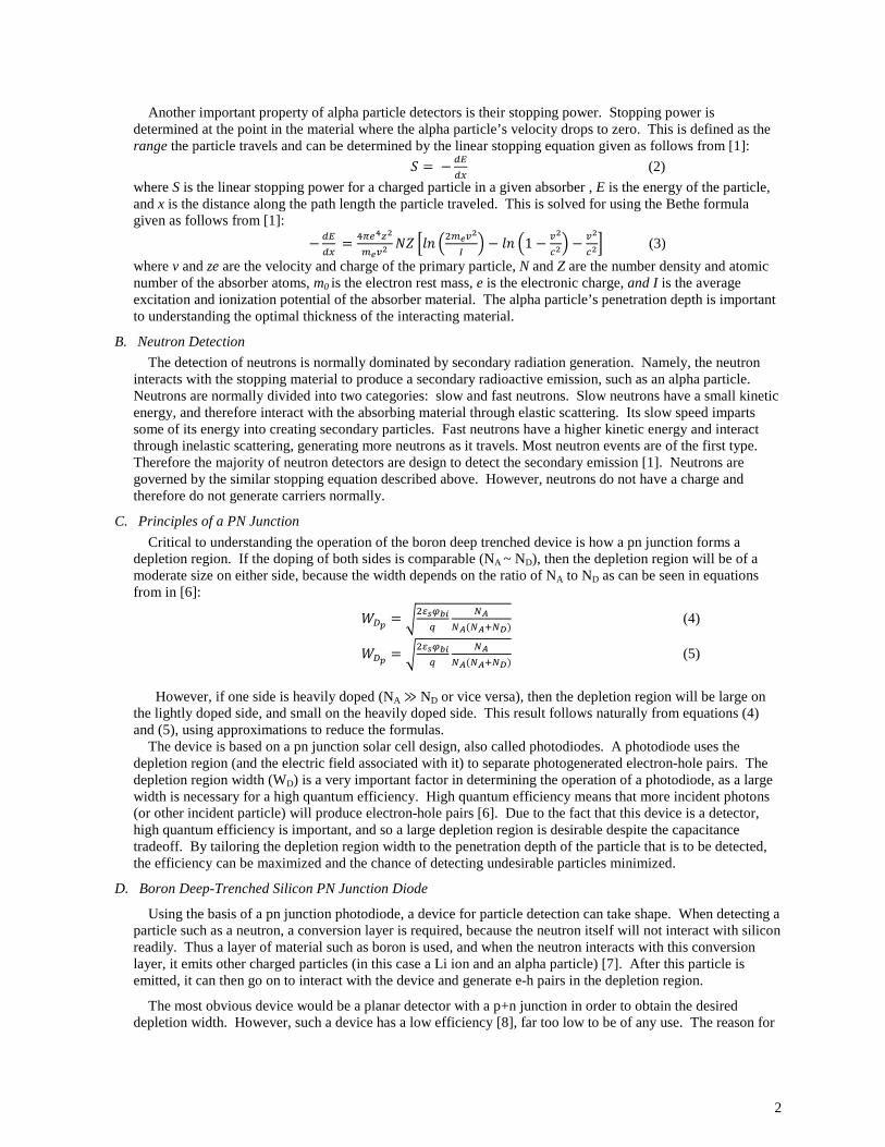
Another important property of alpha particle detectors is their stopping power. Stopping power is determined at the point in the material where the alpha particle’s velocity drops to zero. This is defined as the range the particle travels and can be determined by the linear stopping equation given as follows from [1]:
= − (2)
where S is the linear stopping power for a charged particle in a given absorber , E is the energy of the particle, and x is the distance along the path length the particle traveled. This is solved for using the Bethe formula given as follows from [1]:
− =
− 1 −
" − "# (3)
where v and ze are the velocity and charge of the primary particle, N and Z are the number density and atomic number of the absorber atoms, m0 is the electron rest mass, e is the electronic charge, and I is the average excitation and ionization potential of the absorber material. The alpha particle’s penetration depth is important to understanding the optimal thickness of the interacting material.
B. Neutron Detection
The detection of neutrons is normally dominated by secondary radiation generation. Namely, the neutron interacts with the stopping material to produce a secondary radioactive emission, such as an alpha particle. Neutrons are normally divided into two categories: slow and fast neutrons. Slow neutrons have a small kinetic energy, and therefore interact with the absorbing material through elastic scattering. Its slow speed imparts some of its energy into creating secondary particles. Fast neutrons have a higher kinetic energy and interact through inelastic scattering, generating more neutrons as it travels. Most neutron events are of the first type. Therefore the majority of neutron detectors are design to detect the secondary emission [1]. Neutrons are governed by the similar stopping equation described above. However, neutrons do not have a charge and therefore do not generate carriers normally.
C. Principles of a PN Junction
Critical to understanding the operation of the boron deep trenched device is how a pn junction forms a depletion region. If the doping of both sides is comparable (NA ~ ND), then the depletion region will be of a moderate size on either side, because the width depends on the ratio of NA to ND as can be seen in equations from in [6]:
$%& = '()*+,-
././(./1.2) (4)
$%& = '()*+,-
././(./1.2) (5)
However, if one side is heavily doped (NA ≫ ND or vice versa), then the depletion region will be large on
the lightly doped side, and small on the heavily doped side. This result follows naturally from equations (4) and (5), using approximations to reduce the formulas.
The device is based on a pn junction solar cell design, also called photodiodes. A photodiode uses the depletion region (and the electric field associated with it) to separate photogenerated electron-hole pairs. The depletion region width (WD) is a very important factor in determining the operation of a photodiode, as a large width is necessary for a high quantum efficiency. High quantum efficiency means that more incident photons (or other incident particle) will produce electron-hole pairs [6]. Due to the fact that this device is a detector, high quantum efficiency is important, and so a large depletion region is desirable despite the capacitance tradeoff. By tailoring the depletion region width to the penetration depth of the particle that is to be detected, the efficiency can be maximized and the chance of detecting undesirable particles minimized.
D. Boron Deep-Trenched Silicon PN Junction Diode
Using the basis of a pn junction photodiode, a device for particle detection can take shape. When detecting a particle such as a neutron, a conversion layer is required, because the neutron itself will not interact with silicon readily. Thus a layer of material such as boron is used, and when the neutron interacts with this conversion layer, it emits other charged particles (in this case a Li ion and an alpha particle) [7]. After this particle is emitted, it can then go on to interact with the device and generate e-h pairs in the depletion region.
The most obvious device would be a planar detector with a p+n junction in order to obtain the desired depletion width. However, such a device has a low efficiency [8], far too low to be of any use. The reason for
3
this is that there is a tradeoff with regards to the width of the conversion layer. The conversion layer must be large enough that the incident neutron will interact a high enough percentage of time, and at the same time, the conversion layer must be small enough that the emitted particle can escape the layer to reach the depletion region of the device. This becomes an issue because a neutron can penetrate as much as 50µm into boron before interacting, whereas an alpha particle may only have a range on the order of several microns, depending on its energy [9], and this results in low efficiency for a planar device. In order to increase the efficiency high aspect-ratio trenches are utilized.
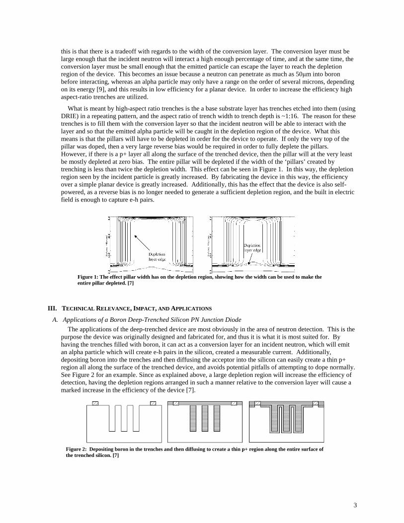
What is meant by high-aspect ratio trenches is the a base substrate layer has trenches etched into them (using DRIE) in a repeating pattern, and the aspect ratio of trench width to trench depth is ~1:16. The reason for these trenches is to fill them with the conversion layer so that the incident neutron will be able to interact with the layer and so that the emitted alpha particle will be caught in the depletion region of the device. What this means is that the pillars will have to be depleted in order for the device to operate. If only the very top of the pillar was doped, then a very large reverse bias would be required in order to fully deplete the pillars. However, if there is a p+ layer all along the surface of the trenched device, then the pillar will at the very least be mostly depleted at zero bias. The entire pillar will be depleted if the width of the ‘pillars’ created by trenching is less than twice the depletion width. This effect can be seen in Figure 1. In this way, the depletion region seen by the incident particle is greatly increased. By fabricating the device in this way, the efficiency over a simple planar device is greatly increased. Additionally, this has the effect that the device is also self-powered, as a reverse bias is no longer needed to generate a sufficient depletion region, and the built in electric field is enough to capture e-h pairs.
III. TECHNICAL RELEVANCE , IMPACT , AND APPLICATIONS
A. Applications of a Boron Deep-Trenched Silicon PN Junction Diode
The applications of the deep-trenched device are most obviously in the area of neutron detection. This is the purpose the device was originally designed and fabricated for, and thus it is what it is most suited for. By having the trenches filled with boron, it can act as a conversion layer for an incident neutron, which will emit an alpha particle which will create e-h pairs in the silicon, created a measurable current. Additionally, depositing boron into the trenches and then diffusing the acceptor into the silicon can easily create a thin p+ region all along the surface of the trenched device, and avoids potential pitfalls of attempting to dope normally. See Figure 2 for an example. Since as explained above, a large depletion region will increase the efficiency of detection, having the depletion regions arranged in such a manner relative to the conversion layer will cause a marked increase in the efficiency of the device [7].
Figure 1: The effect pillar width has on the depletion region, showing how the width can be used to make the entire pillar depleted. [7]
Figure 2: Depositing boron in the trenches and then diffusing to create a thin p+ region along the entire surface of the trenched silicon. [7]

4
B. Applications of Alpha Particle Detectors
The applications of alpha particle detectors include uses in neutron detection [7], chip manufacturing [10, 11], smoke detection [12], radon detection [13, 14], earthquake prediction [14], alphavolatics [15], and homeland security [16]. While many of these applications are well researched, the devices used in alpha particle detection suffer from numerous faults such as poor radiation hardness or poor energy resolution. However, most research into developing better alpha particle detectors has reached a plateau. Still, the field of neutron detection is currently of increasing interest [7, 11], yet there is no direct means of detecting neutrons [1]. Therefore, as the primary method for neutron detection produces alpha radiation, the need to interpret the alpha particle detection capabilities of neutron detectors becomes apparent.
C. Applications of Neutron Detectors
The applications of neutron detectors include homeland security, detection of special nuclear materials [19], nuclear safety in nuclear reactors, measurements in particle physics [17], medical sciences [18], and cosmic rays [19] detection. However, many modern neutron detectors are expensive and large in size. Solid state neutron detectors offer a way to fabricate relatively inexpensive, small detectors in large quantities to provide a scalable solution to neutron detection applications [7].
IV. EXPERIMENTAL RESULTS
A. Hand Calculations
Some basic hand calculations of a few parameters were performed. Their results are listed in Table 1 along with simulation and measured results.
Table 1 WD (µm) 567 (V) C/A (nF/cm2) R (MΩ) Hand 3.03575 0.714 2.592 20.5905 Simulated 2.5 0.7 * N/A Measured N/A 0.3 N/A **
The depletion layer width is obtained by adding equations (4) and (5) from above. The result is approximately 3.03575µm, assuming 1018 cm-3 doping in the p+ region, and 1014 cm-3 doping in the n region, 89: is calculated to be 0.714V using the following equation from [6]:
;9: = <=- ln ./.2
@, (6)
The capacitance is calculated by using the following equation from LiCausi et al. [7]: AB = CC.E×E.EG×CHI
JKLMNO1J&,PPQLRJKLMNO
J2 + J&,PPQLTJ2&J21U&,PPQL V W × XT (7)
This equation was obtained through manipulation of the general Capacitance/Area equationY = Z[:\/$%. The result of the hand calculations is that the capacitance at zero bias is 2.592nF/cm2.
The following formula is used to calculate the resistance of the device: ^ = _`/\ (8)
Due to the size of the pillar (45µm x 1µm), the device resistance is found to be quite large. Hand calculations yield a resistance of 20.5905 MΩ for one entire pillar.
B. Simulations
1) GEANT 4 Originally, the GEANT 4 software was envisioned to be used to calculate the stopping range of an alpha
particle in the boron deep trenched silicon pn junction diode. However, it was discovered this software was too difficult to use given the users knowledge of programming. Instead, hand calculations of the stopping range of an alpha particle in boron and in silicon+1µm of aluminum are provided. Using equations (2) and
Table 1: Specific device parameter values as derived from hand, simulation and measured data at 0 bias *The simulation results are not accurate due to several device parameters **A zero bias result is not available.
5
(3) mentioned above it was determined an alpha particle travels at approximately 15µm into boron and 25µm into silicon.
2) MEDICI
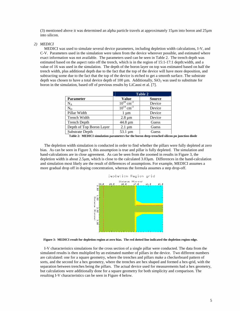
MEDICI was used to simulate several device parameters, including depletion width calculations, I-V, and C-V. Parameters used in the simulation were taken from the device wherever possible, and estimated where exact information was not available. The parameters used can be seen in Table 2. The trench depth was estimated based on the aspect ratio off the trench, which is in the region of 15:1-17:1 depth:width, and a value of 16 was used in the simulation. The depth of the boron layer on top was estimated based on half the trench width, plus additional depth due to the fact that the top of the device will have more deposition, and subtracting some due to the fact that the top of the device is etched to get a smooth surface. The substrate depth was chosen to have a total device depth of 100 µm. Additionally, SiO2 was used to substitute for boron in the simulation, based off of previous results by LiCausi et al. [7].
Table 2 Parameter Value Source NA 1018 cm-3 Device ND 1014 cm-3 Device Pillar Width 1 µm Device Trench Width 2.8 µm Device Trench Depth 44.8 µm Guess Depth of Top Boron Layer 2.1 µm Guess Substrate Depth 53.1 µm Guess
The depletion width simulation is conducted in order to find whether the pillars were fully depleted at zero
bias. As can be seen in Figure 3, this assumption is true and pillar is fully depleted. The simulation and hand-calculations are in close agreement. As can be seen from the zoomed in results in Figure 3, the depletion width is about 2.5µm, which is close to the calculated 3.03µm. Differences in the hand-calculation and simulation most likely are the result of differences of assumptions. For example, MEDICI assumes a more gradual drop off in doping concentration, whereas the formula assumes a step drop-off.
I-V characteristics simulations for the cross section of a single pillar were conducted. The data from the
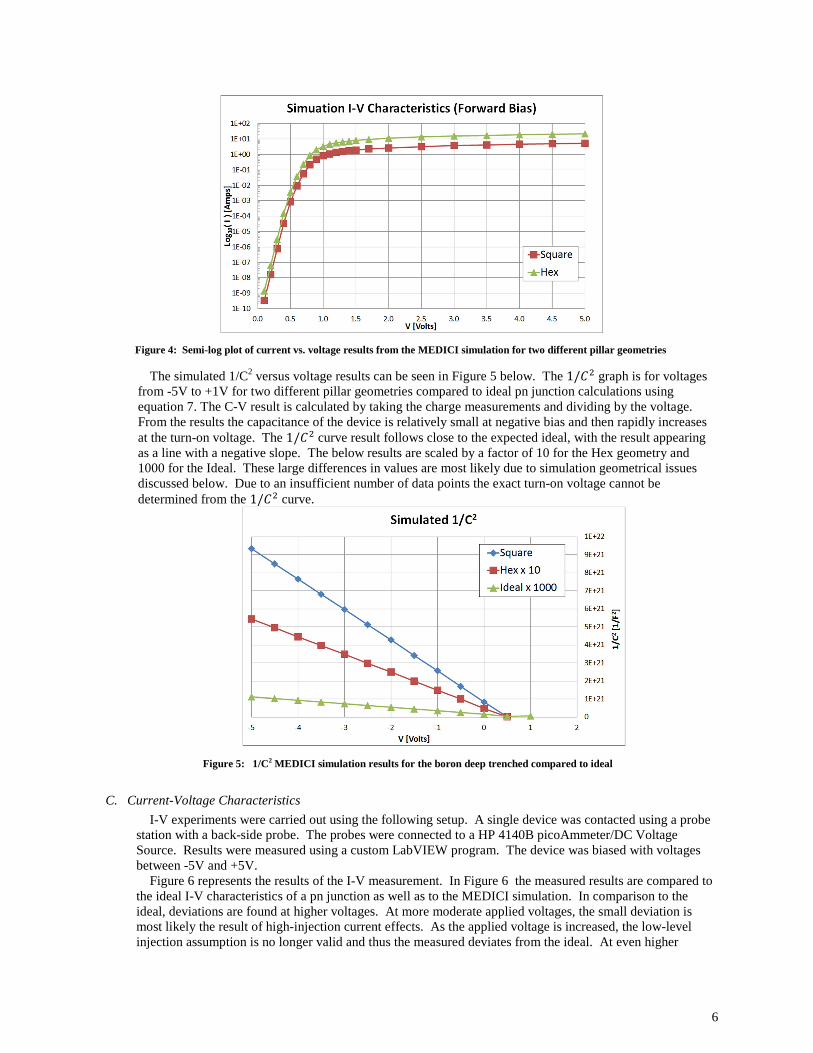
simulated results is then multiplied by an estimated number of pillars in the device. Two different numbers are calculated: one for a square geometry, where the trenches and pillars make a checkerboard pattern of sorts, and the second for a hex geometry, where the trenches are hex shaped and formed a hex-grid, with the separation between trenches being the pillars. The actual device used for measurements had a hex geometry, but calculations were additionally done for a square geometry for both simplicity and comparison. The resulting I-V characteristics can be seen in Figure 4 below.
Figure 3: MEDICI result for depletion region at zero bias. The red dotted line indicated the depletion region edge.
Table 2: MEDICI simulation parameters for the boron deep-trenched silicon pn junction diode
6
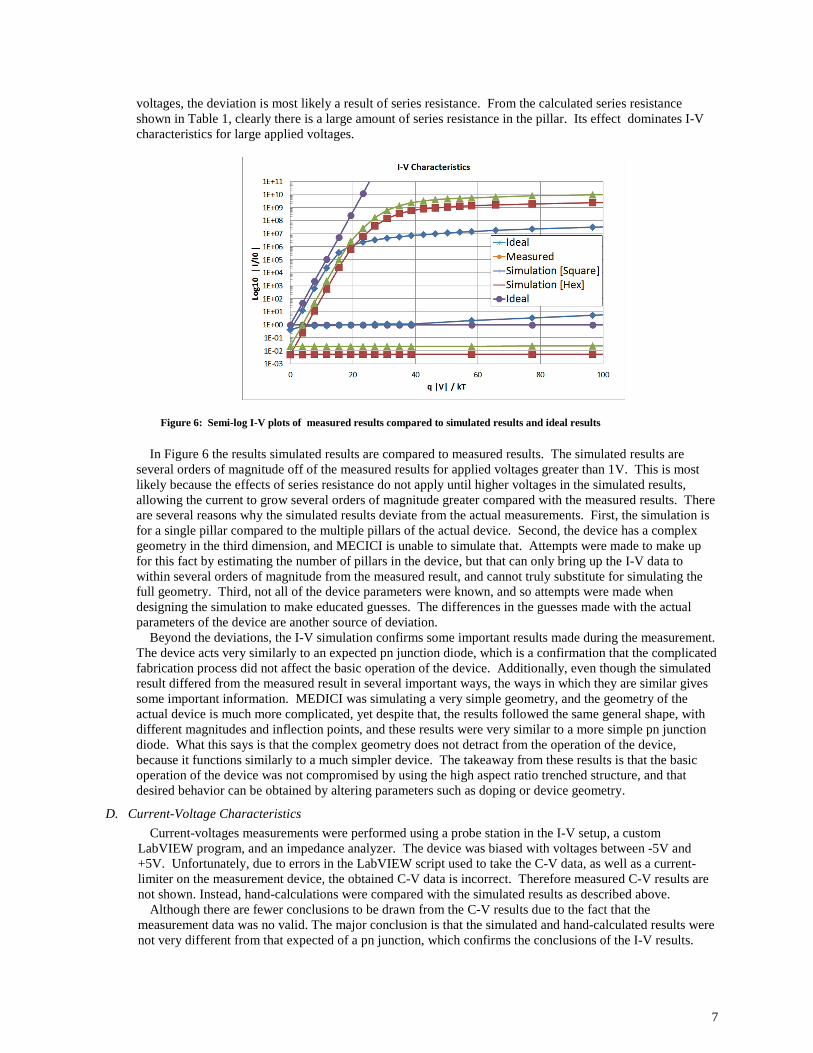
The simulated 1/C2 versus voltage results can be seen in Figure 5 below. The 1/Y graph is for voltages from -5V to +1V for two different pillar geometries compared to ideal pn junction calculations using equation 7. The C-V result is calculated by taking the charge measurements and dividing by the voltage. From the results the capacitance of the device is relatively small at negative bias and then rapidly increases at the turn-on voltage. The 1/Y curve result follows close to the expected ideal, with the result appearing as a line with a negative slope. The below results are scaled by a factor of 10 for the Hex geometry and 1000 for the Ideal. These large differences in values are most likely due to simulation geometrical issues discussed below. Due to an insufficient number of data points the exact turn-on voltage cannot be determined from the 1/Y curve.
C. Current-Voltage Characteristics
I-V experiments were carried out using the following setup. A single device was contacted using a probe station with a back-side probe. The probes were connected to a HP 4140B picoAmmeter/DC Voltage Source. Results were measured using a custom LabVIEW program. The device was biased with voltages between -5V and +5V.
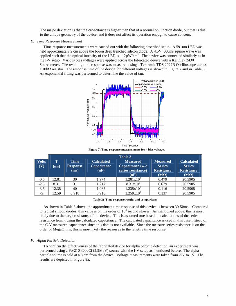
Figure 6 represents the results of the I-V measurement. In Figure 6 the measured results are compared to the ideal I-V characteristics of a pn junction as well as to the MEDICI simulation. In comparison to the ideal, deviations are found at higher voltages. At more moderate applied voltages, the small deviation is most likely the result of high-injection current effects. As the applied voltage is increased, the low-level injection assumption is no longer valid and thus the measured deviates from the ideal. At even higher
Figure 4: Semi-log plot of current vs. voltage results from the MEDICI simulation for two different p illar geometries
Figure 5: 1/C2 MEDICI simulation results for the boron deep trenched compared to ideal
7
voltages, the deviation is most likely a result of series resistance. From the calculated series resistance shown in Table 1, clearly there is a large amount of series resistance in the pillar. Its effect dominates I-V characteristics for large applied voltages.
In Figure 6 the results simulated results are compared to measured results. The simulated results are
several orders of magnitude off of the measured results for applied voltages greater than 1V. This is most likely because the effects of series resistance do not apply until higher voltages in the simulated results, allowing the current to grow several orders of magnitude greater compared with the measured results. There are several reasons why the simulated results deviate from the actual measurements. First, the simulation is for a single pillar compared to the multiple pillars of the actual device. Second, the device has a complex geometry in the third dimension, and MECICI is unable to simulate that. Attempts were made to make up for this fact by estimating the number of pillars in the device, but that can only bring up the I-V data to within several orders of magnitude from the measured result, and cannot truly substitute for simulating the full geometry. Third, not all of the device parameters were known, and so attempts were made when designing the simulation to make educated guesses. The differences in the guesses made with the actual parameters of the device are another source of deviation.
Beyond the deviations, the I-V simulation confirms some important results made during the measurement. The device acts very similarly to an expected pn junction diode, which is a confirmation that the complicated fabrication process did not affect the basic operation of the device. Additionally, even though the simulated result differed from the measured result in several important ways, the ways in which they are similar gives some important information. MEDICI was simulating a very simple geometry, and the geometry of the actual device is much more complicated, yet despite that, the results followed the same general shape, with different magnitudes and inflection points, and these results were very similar to a more simple pn junction diode. What this says is that the complex geometry does not detract from the operation of the device, because it functions similarly to a much simpler device. The takeaway from these results is that the basic operation of the device was not compromised by using the high aspect ratio trenched structure, and that desired behavior can be obtained by altering parameters such as doping or device geometry.
D. Current-Voltage Characteristics
Current-voltages measurements were performed using a probe station in the I-V setup, a custom LabVIEW program, and an impedance analyzer. The device was biased with voltages between -5V and +5V. Unfortunately, due to errors in the LabVIEW script used to take the C-V data, as well as a current-limiter on the measurement device, the obtained C-V data is incorrect. Therefore measured C-V results are not shown. Instead, hand-calculations were compared with the simulated results as described above.
Although there are fewer conclusions to be drawn from the C-V results due to the fact that the measurement data was no valid. The major conclusion is that the simulated and hand-calculated results were not very different from that expected of a pn junction, which confirms the conclusions of the I-V results.
Figure 6: Semi-log I-V plots of measured results compared to simulated results and ideal results
8
The major deviation is that the capacitance is higher than that of a normal pn junction diode, but that is due to the unique geometry of the device, and it does not affect its operation enough to cause concern.
E. Time Response Measurement
Time response measurements were carried out with the following described setup. A 591nm LED was held approximately 2 cm above the boron deep trenched silicon diode. A 4.5V, 500ms square wave was applied such that the optical intensity of the LED is 112µW/cm2. The device was connected similarly as in the I-V setup. Various bias voltages were applied across the fabricated device with a Keithley 2430 Sourcemeter. The resulting time response was measured using a Tektronic TDS 2022B Oscilloscope across a 10kΩ resistor. The response time of the device for different voltages is shown in Figure 7 and in Table 3. An exponential fitting was performed to determine the value of tau.
As shown in Table 3 above, the approximate time response of this device is between 30-50ms. Compared to typical silicon diodes, this value is on the order of 104 second slower. As mentioned above, this is most likely due to the large resistance of the device. This is assumed true based on calculations of the series resistance from τ using the calculated capacitance. The calculated capacitance is used in this case instead of the C-V measured capacitance since this data is not available. Since the measure series resistance is on the order of MegaOhms, this is most likely the reason as to the lengthy time response.
F. Alpha Particle Detection
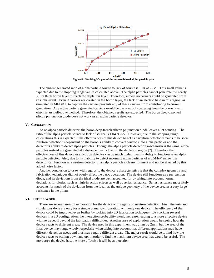
To confirm the effectiveness of the fabricated device for alpha particle detection, an experiment was performed using a Po-210 300uCi (5.5MeV) source with the I-V setup as mentioned before. The alpha particle source is held at a 3 cm from the device. Voltage measurements were taken from -5V to 1V. The results are depicted in Figure 8a.
Table 3 Volts (V)
Τ
(ms) Time
Response (ms)
Calculated Capacitance
(nF)
Measured Capacitance (w/o series resistance)
(nF)
Measured Series
Resistance (MΩ)
Calculated Series
Resistance (MΩ)
-0.5 12.81 30 1.974 1.281x10³ 6.479 20.5905 -2.5 8.31 31 1.217 8.31x10² 6.679 20.5905 -3.5 12.35 40 1.065 1.235x10³ 0.116 20.5905 -5 12.59 0.918 0.918 1.259x10³ 0.137 20.5905
Table 3: Time response results and comparisons
Figure 7: Time response measurements for 4 bias voltages
9
The current generated ratio of alpha particle source to lack of source is 1.04 at -5 V. This small value is
expected due to the stopping range values calculated above. The alpha particles cannot penetrate the nearly 50µm thick boron layer to reach the depletion layer. Therefore, almost no carriers could be generated from an alpha event. Even if carriers are created in the boron layer, the lack of an electric field in this region, as simulated in MEDICI, to capture the carriers prevents any of these carriers from contributing to current generation. Any alpha particle generated carriers would be the result of scattering from the boron layer, which is an ineffective method. Therefore, the obtained results are expected. The boron deep-trenched silicon pn junction diode does not work as an alpha particle detector.
V. CONCLUSION
As an alpha particle detector, the boron deep-trench silicon pn junction diode leaves a lot wanting. The ratio of the alpha particle source to lack of source is 1.04 at -5V. However, due to the stopping range calculations this is expected. The effectiveness of this device to act as a neutron detector remains to be seen. Neutron detection is dependent on the boron’s ability to convert neutrons into alpha particles and the detector’s ability to detect alpha particles. Though the alpha particle detection mechanism is the same, alpha particles instead are generated at a distance much closer to the depletion region [7]. Therefore the effectiveness of this device as a neutron detector can be much higher than its ability to function as an alpha particle detector. Also, due to its inability to detect incoming alpha particles of a 5.5MeV range, this detector can function as a neutron detector in an alpha particle rich environment and not be affected by this added noise factor.
Another conclusion to draw with regards to the device’s characteristics is that the complex geometry and fabrication techniques did not overly affect the basic operation. The device still functions as a pn junction diode, and its deviations from the ideal diode are well accounted for by taking into account normal deviations for diodes, such as high-injection effects as well as series resistance. Series resistance most likely accounts for much of the deviation from the ideal, as the unique geometry of the device creates a very large resistance in the pillars.
VI. FUTURE WORK
There are several areas of exploration for the device with regards to neutron detection. First, the tests and simulations done are only for a simple planar configuration, with only one device. The efficiency of the device could be improved even further by looking into 3D fabrication techniques. By stacking several devices in a 3D configuration, the interaction probability would increase, leading to a more effective device with no tradeoff beyond the fabrication difficulties. Another area of exploration would be seeing how the device reacts to different areas. The device used in this experiment was 2mm by 2mm, but the area of the final device may range widely, especially when taking into account that different applications may have different detection needs and thus may require different areas. The major result would be to find how the device reacts to scaling down and up, in order to find the maximum device area that would be useful. The more area the device has, the more effective it will be at detection.
Figure 8: Semi-log I-V plot of the reverse biased alpha particle gain
10
REFERENCES [1] G.F. Knoll, Radiation Detection and Measurement, 4th Ed. Hoboken, NJ: John Wiley & Sons, 2010. [2] J.W. Mayer, “Method of measuring nuclear radiation utilizing a semiconductor crystal having a lithium compensated intrinsic region,” U.S.
Patent 3 225 198 Dec. 21, 1965. [3] J. Denney, P. Verdes, S.S. Friedland, S. Oaks, and F. Keywall, “Solid state radiation detector with wide depletion region,” U.S. Patent 3 110
806 Nov. 12 1963. [4] M.J. Raju, “The use of the miniature silicon diode as a radiation dosemeter,” Phys. Med Biol., vol. 7, p 371, Jul 1966. [5] R.F. Pierret, Semiconductor Device Fundamentals, Reading, MA: Addison-Wesley Publishing Company, Inc, 1996. [6] S.M. Sze and K.K. Ng, Physics of Semiconductor Devices, 3rd Ed. Hoboken, NJ: John Wiley & Sons, 2007. [7] N. LiCausi, J. Dingley, Y. Danon, J.Q. Lu, and I.B. Bhat, “A novel solid state self-powered neutron detector,” Proc. of SPIE, vol. 7079,
Sep. 2008. [8] C. Perillo, F. Sacchetti, O. Toker, and N.J. Rhodes, “Solid state neutron detectors,” Nuclear Inst. And Meth. in Physics Res. A, vol. 378, pp
541-551, 1996. [9] Y. Danon, I. Bhat, and J.Q. Lu, “A novel solid state self-powered neutron detector,” May 2007, unpublished [10] B.J. Masters, “Experimental studies of ZnS alpha particle counters and methods for minimizing detector background,” Rel. Phys. Symp., pp
269-274, 1980. [11] M.S. Gordon, K.P. Rodbell, D.F. Heidel, C. Cabral, E.H. Cannon, D.D. Reinhardt, “Single-event-upset and alpha-particle emission rate
measurement techniques,” IBM J. of Research and Develop., vol. 52, no. 3, pp 265-273, May 2008. [12] J. Bryant, J.H. Howes, D.W.S. Smout, “Smoke Detectors,” U.S. Patent 4 361 763, Nov. 1982. [13] C. Papastefanou, “An overview of instrumentation for measuring radon in soil gas and groundwaters,” J. of Environmental Radioactivity,
vol 63, pp 271-283, May 2002. [14] J. Planinić, V. Radolić, and B. Vuković, “Radon as an earthquake precursor,” Nuclear Inst. And Meth. in Physics Res. A, vol. 530, no. 3, pp.
568-574, Sept. 2004. [15] C.D. Cress, B.J. Landi, R.P. Raffaelle, and David M. Wilt, “InGaP alpha voltaic batteries: Synthesis, modeling, and radiation technique,” J.
Appl. Phys., vol. 100, Dec. 2006. [16] P.H. Willms and L.E. Atlas, “Detection of nuclear materials hidden inside cargo shipments by using sensor fusion technique,” U.S. Patent 7
701 336, Apr. 2010. [17] J.F. Beacom and M.R. Vagins, “Antineutrino Spectroscopy with Large Water Čerenkov Detectors,” Phys. Rev. Lett., vol 93, no. 17, Oct.
2004 [18] B. Schillinger, J. Baumann, H. Gebele, R. Schaetzing, H. Schaller, M. Schuster, “A new fast and large area neutron detector using a novel
image plate readout technique,” Appl. Radiation and Isotopes, vol. 61, no. 4, pp. 451-454, Oct. 2004 [19] W.R. Webber and J.A. Lockwood, “Characteristics of the 22-Year Modulation of Cosmic Rays as Seen by Neutron Monitors,” J. of
Geophysical Research, vol. 93, no. a8, pp 8753-8740, May 1988
11
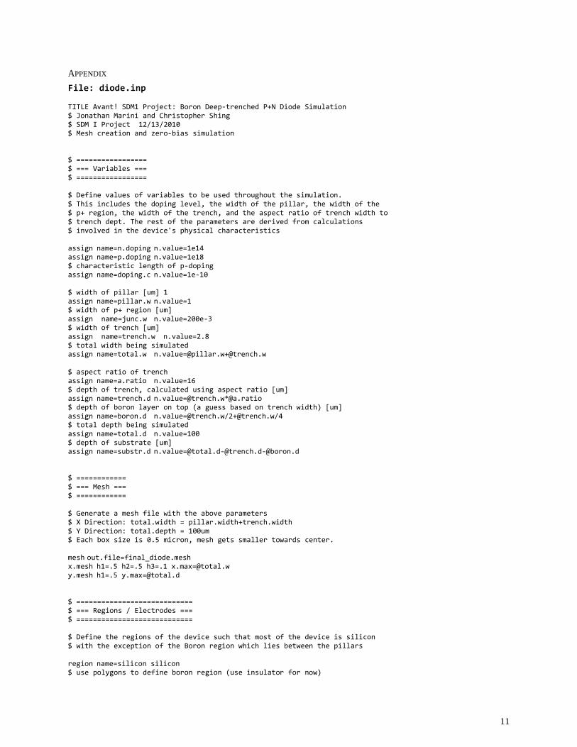
APPENDIX
File: diode.inp TITLE Avant! SDM1 Project: Boron Deep-trenched P+N Diode Simulation $ Jonathan Marini and Christopher Shing $ SDM I Project 12/13/2010 $ Mesh creation and zero-bias simulation $ ================= $ === Variables === $ ================= $ Define values of variables to be used throughout the simulation. $ This includes the doping level, the width of the pillar, the width of the
$ p+ region, the width of the trench, and the aspect ratio of trench width to $ trench dept. The rest of the parameters are derived from calculations $ involved in the device's physical characteristics assign name=n.doping n.value=1e14 assign name=p.doping n.value=1e18 $ characteristic length of p-doping assign name=doping.c n.value=1e-10 $ width of pillar [um] 1 assign name=pillar.w n.value=1 $ width of p+ region [um] assign name=junc.w n.value=200e-3 $ width of trench [um] assign name=trench.w n.value=2.8 $ total width being simulated assign name=total.w [email protected][email protected]
$ aspect ratio of trench assign name=a.ratio n.value=16 $ depth of trench, calculated using aspect ratio [um] assign name=trench.d [email protected]*@a.ratio $ depth of boron layer on top (a guess based on trench width) [um] assign name=boron.d [email protected]/[email protected]/4 $ total depth being simulated assign name=total.d n.value=100 $ depth of substrate [um] assign name=substr.d [email protected]@[email protected] $ ============ $ === Mesh === $ ============
$ Generate a mesh file with the above parameters $ X Direction: total.width = pillar.width+trench.width $ Y Direction: total.depth = 100um $ Each box size is 0.5 micron, mesh gets smaller towards center. mesh out.file=final_diode.mesh x.mesh h1=.5 h2=.5 h3=.1 [email protected] y.mesh h1=.5 [email protected] $ ============================ $ === Regions / Electrodes === $ ============================ $ Define the regions of the device such that most of the device is silicon $ with the exception of the Boron region which lies between the pillars
region name=silicon silicon $ use polygons to define boron region (use insulator for now)
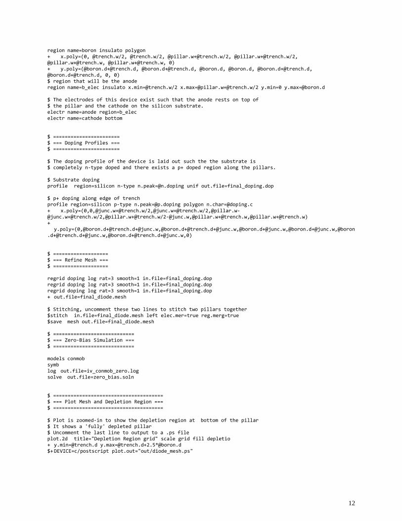
12
region name=boron insulato polygon + x.poly=(0, @trench.w/2, @trench.w/2, @[email protected]/2, @[email protected]/2, @[email protected], @[email protected], 0) + y.poly=(@[email protected], @[email protected], @boron.d, @boron.d, @[email protected], @[email protected], 0, 0) $ region that will be the anode region name=b_elec insulato [email protected]/2 [email protected][email protected]/2 y.min=0 [email protected] $ The electrodes of this device exist such that the anode rests on top of
$ the pillar and the cathode on the silicon substrate. electr name=anode region=b_elec electr name=cathode bottom $ ======================= $ === Doping Profiles === $ ======================= $ The doping profile of the device is laid out such the the substrate is $ completely n-type doped and there exists a p+ doped region along the pillars. $ Substrate doping profile region=silicon n-type [email protected] unif out.file=final_doping.dop $ p+ doping along edge of trench profile region=silicon p-type [email protected] polygon [email protected]
+ x.poly=(0,0,@[email protected]/2,@[email protected]/2,@[email protected][email protected]/2,@[email protected]/[email protected],@[email protected],@[email protected]) + y.poly=(0,@[email protected][email protected],@[email protected][email protected],@[email protected],@[email protected],@[email protected][email protected],@[email protected][email protected],0) $ =================== $ === Refine Mesh === $ =================== regrid doping log rat=3 smooth=1 in.file=final_doping.dop regrid doping log rat=3 smooth=1 in.file=final_doping.dop regrid doping log rat=3 smooth=1 in.file=final_doping.dop + out.file=final_diode.mesh
$ Stitching, uncomment these two lines to stitch two pillars together $stitch in.file=final_diode.mesh left elec.mer=true reg.merg=true $save mesh out.file=final_diode.mesh $ ============================ $ === Zero-Bias Simulation === $ ============================ models conmob symb log out.file=iv_conmob_zero.log solve out.file=zero_bias.soln $ ====================================== $ === Plot Mesh and Depletion Region === $ ======================================
$ Plot is zoomed-in to show the depletion region at bottom of the pillar $ It shows a 'fully' depleted pillar $ Uncomment the last line to output to a .ps file plot.2d title="Depletion Region grid" scale grid fill depletio + [email protected] [email protected]+2.5*@boron.d $+ DEVICE=c/postscript plot.out="out/diode_mesh.ps"
13
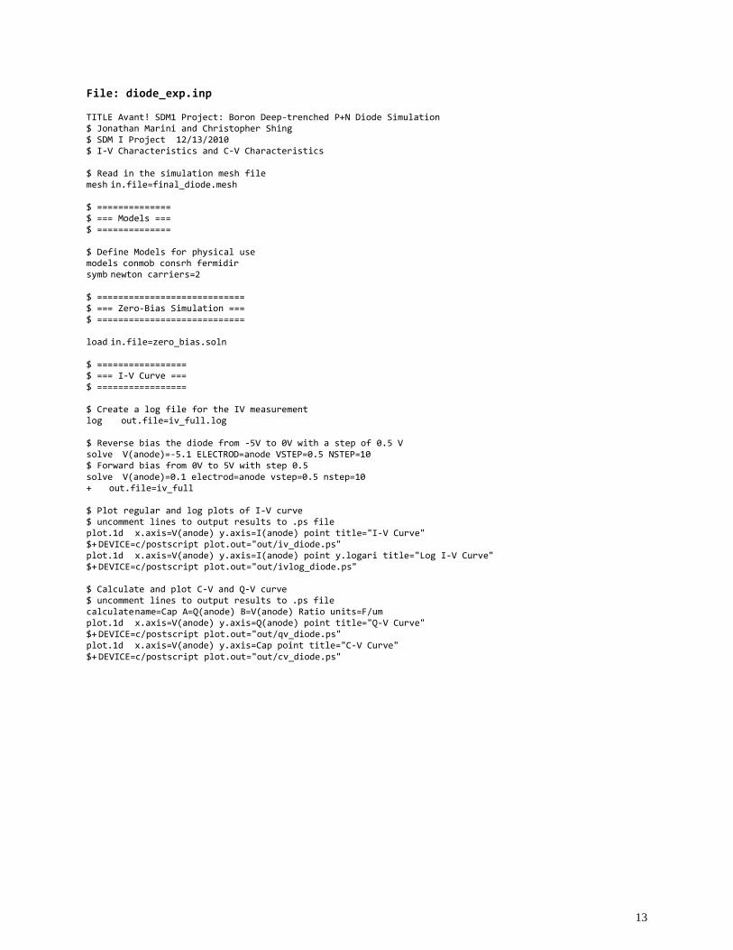
File: diode_exp.inp TITLE Avant! SDM1 Project: Boron Deep-trenched P+N Diode Simulation $ Jonathan Marini and Christopher Shing $ SDM I Project 12/13/2010 $ I-V Characteristics and C-V Characteristics $ Read in the simulation mesh file mesh in.file=final_diode.mesh $ ============== $ === Models === $ ============== $ Define Models for physical use models conmob consrh fermidir symb newton carriers=2
$ ============================ $ === Zero-Bias Simulation === $ ============================ load in.file=zero_bias.soln $ ================= $ === I-V Curve === $ ================= $ Create a log file for the IV measurement log out.file=iv_full.log $ Reverse bias the diode from -5V to 0V with a step of 0.5 V solve V(anode)=-5.1 ELECTROD=anode VSTEP=0.5 NSTEP=10 $ Forward bias from 0V to 5V with step 0.5
solve V(anode)=0.1 electrod=anode vstep=0.5 nstep=10 + out.file=iv_full $ Plot regular and log plots of I-V curve $ uncomment lines to output results to .ps file plot.1d x.axis=V(anode) y.axis=I(anode) point title="I-V Curve" $+ DEVICE=c/postscript plot.out="out/iv_diode.ps" plot.1d x.axis=V(anode) y.axis=I(anode) point y.logari title="Log I-V Curve" $+ DEVICE=c/postscript plot.out="out/ivlog_diode.ps" $ Calculate and plot C-V and Q-V curve $ uncomment lines to output results to .ps file calculate name=Cap A=Q(anode) B=V(anode) Ratio units=F/um plot.1d x.axis=V(anode) y.axis=Q(anode) point title="Q-V Curve" $+ DEVICE=c/postscript plot.out="out/qv_diode.ps" plot.1d x.axis=V(anode) y.axis=Cap point title="C-V Curve"
$+ DEVICE=c/postscript plot.out="out/cv_diode.ps"