altera high-definition multimedia interface (hdmi) ip … · altera high-definition multimedia...
TRANSCRIPT
Altera High-Definition MultimediaInterface (HDMI) IP Core User Guide
Last updated for Quartus Prime Design Suite: 16.0
Subscribe
Send Feedback
UG-HDMI2016.05.02
101 Innovation DriveSan Jose, CA 95134www.altera.com
Contents
HDMI Quick Reference.......................................................................................1-1
HDMI Overview.................................................................................................. 2-1Resource Utilization.................................................................................................................................... 2-5
HDMI Getting Started.........................................................................................3-1Installing and Licensing IP Cores.............................................................................................................. 3-1Specifying IP Core Parameters and Options............................................................................................3-2
HDMI Source.......................................................................................................4-1Source Functional Description.................................................................................................................. 4-1
Source TMDS/TERC4 Encoder..................................................................................................... 4-2Source Video Resampler................................................................................................................. 4-2Source Window of Opportunity Generator................................................................................. 4-7Source Auxiliary Packet Encoder...................................................................................................4-8Source Auxiliary Packet Generators............................................................................................4-10Source Auxiliary Data Path Multiplexers................................................................................... 4-10Source Auxiliary Control Port..................................................................................................... 4-10Source Audio Encoder.................................................................................................................. 4-14
Source Parameters..................................................................................................................................... 4-17Source Interfaces........................................................................................................................................ 4-18Source Clock Tree......................................................................................................................................4-23
HDMI Sink...........................................................................................................5-1Sink Functional Description.......................................................................................................................5-1
Sink Channel Word Alignment and Deskew...............................................................................5-2Sink TMDS/TERC4 Decoder......................................................................................................... 5-3Sink Video Resampler..................................................................................................................... 5-4Sink Auxiliary Decoder................................................................................................................... 5-4Sink Auxiliary Packet Capture....................................................................................................... 5-6Sink Auxiliary Data Port................................................................................................................. 5-9Sink Audio Decoding.................................................................................................................... 5-10
Sink Parameters..........................................................................................................................................5-14Sink Interfaces............................................................................................................................................ 5-15
Avalon-MM SCDC Management Interface............................................................................... 5-22Status and Control Data Channel Interface............................................................................... 5-22
Sink Clock Tree.......................................................................................................................................... 5-22
HDMI Hardware Demonstration....................................................................... 6-1
TOC-2
Altera Corporation
Hardware Demonstration Components...................................................................................................6-1Transceiver Native PHY (RX)—Arria V and Stratix V Devices................................................6-4Transceiver Native PHY (RX)—Arria 10 Devices.......................................................................6-8Altera PLL IP Cores....................................................................................................................... 6-11Altera PLL Reconfig IP Core........................................................................................................ 6-13Multirate Reconfig Controller (RX)............................................................................................ 6-13Oversampler (RX)..........................................................................................................................6-14DCFIFO...........................................................................................................................................6-15Sink Display Data Channel (DDC) & Status and Control Data Channel (SCDC)...............6-15Transceiver Reconfiguration Controller.....................................................................................6-15VIP Bypass and Audio, Auxiliary and InfoFrame Buffers....................................................... 6-16Transceiver Native PHY (TX)—Arria V and Stratix V Devices............................................. 6-16Transceiver Native PHY (TX)—Arria 10 Devices.....................................................................6-18Transceiver PHY Reset Controller.............................................................................................. 6-20Transceiver fPLL IP Core..............................................................................................................6-20Oversampler (TX)..........................................................................................................................6-23Clock Enable Generator................................................................................................................ 6-23Qsys System.................................................................................................................................... 6-23
HDMI Hardware Demonstration Requirements.................................................................................. 6-26Demonstration Walkthrough...................................................................................................................6-27
Set Up the Hardware..................................................................................................................... 6-28Copy the Design Files....................................................................................................................6-28Build and Compile the Design..................................................................................................... 6-28View the Results............................................................................................................................. 6-29
HDMI Simulation Example................................................................................ 7-1Simulation Walkthrough............................................................................................................................ 7-2
HDMI IP Core User Guide Archives..................................................................A-1
Document Revision History for HDMI User Guide.......................................... B-1
TOC-3
Altera Corporation

HDMI Quick Reference 12016.05.02
UG-HDMI Subscribe Send Feedback
The Altera High-Definition Multimedia Interface (HDMI) IP core provides support for next-generationvideo display interface technology.
Information Description
Release InformationVersion 16.0Release May 2016Ordering Code IP-HDMI
© 2016 Altera Corporation. All rights reserved. ALTERA, ARRIA, CYCLONE, ENPIRION, MAX, MEGACORE, NIOS, QUARTUS and STRATIX words and logos aretrademarks of Altera Corporation and registered in the U.S. Patent and Trademark Office and in other countries. All other words and logos identified astrademarks or service marks are the property of their respective holders as described at www.altera.com/common/legal.html. Altera warrants performanceof its semiconductor products to current specifications in accordance with Altera's standard warranty, but reserves the right to make changes to anyproducts and services at any time without notice. Altera assumes no responsibility or liability arising out of the application or use of any information,product, or service described herein except as expressly agreed to in writing by Altera. Altera customers are advised to obtain the latest version of devicespecifications before relying on any published information and before placing orders for products or services.
ISO9001:2008Registered
www.altera.com101 Innovation Drive, San Jose, CA 95134

Information Description
IP Core Information
Core Features • Conforms to the High-Definition MultimediaInterface (HDMI) specification versions 1.4 and2.0
• Supports transmitter and receiver on a singledevice transceiver quad
• Supports pixel frequency up to 594 MHz• Supports RGB and YCbCr 444, 422, and 420 color
modes• Accepts standard H-SYNC, V-SYNC, data enable,
RGB video format, and YCbCr video format• Supports 2-channel and 8-channel audios• Supports 1, 2, or 4 symbols per clock• Supports 8, 10, 12, or 16 bits per color (bpc)• Supports Digital Visual Interface (DVI)
Typical Application • Interfaces within a PC and monitor• External display connections, including interfaces
between a PC and monitor or projector, betweena PC and TV, or between a device such as a DVDplayer and TV display
Device Family Supports Arria® 10, Arria V, and Stratix V FPGAdevices
Design Tools • Quartus® Prime software for IP design instantia‐tion and compilation
• TimeQuest Timing Analyzer in the QuartusPrime software for timing analysis
• ModelSim-Altera/SE software for designsimulation
Related InformationHDMI IP Core User Guide Archives on page 8-1Provides a list of user guides for previous versions of the HDMI IP core.
1-2 HDMI Quick ReferenceUG-HDMI
2016.05.02
Altera Corporation HDMI Quick Reference
Send Feedback
HDMI Overview 22016.05.02
UG-HDMI Subscribe Send Feedback
The Altera High-Definition Multimedia Interface (HDMI) IP core provides support for next generationvideo display interface technology.
The HDMI standard specifies a digital communications interface for use in both internal and externalconnections:
• Internal connections—interface within a PC and monitor• External display connections—interface between a PC and monitor or projector, between a PC and
TV, or between a device such a DVD player and TV display.
The HDMI system architecture consists of sinks and sources. A device may have one or more HDMIinputs and outputs.
The HDMI cable and connectors carry four differential pairs that make up the Transition MinimizedDifferential Signaling (TMDS) data and clock channels. You can use these channels to carry video, audio,and auxiliary data.
The HDMI also carries a Video Electronics Standards Association (VESA) Display Data Channel (DDC)and Status and Control Data Channel (SCDC). The DDC configures and exchanges status between asingle source and a single sink. The source uses the DDC to read the sink's Enhanced Extended DisplayIdentification Data (E-EDID) to discover the sink's configuration and capabilities. The SCDC supportsthe sink's read requests.
The optional Consumer Electronics Control (CEC) protocol provides high-level control functionsbetween various audio visual products in your environment.
The optional HDMI Ethernet and Audio Return Channel (HEAC) provides Ethernet compatible datanetworking between connected devices and an audio return channel in the opposite direction of TMDS.The HEAC also uses Hot-Plug Detect (HPD) line for signal transmission.
© 2016 Altera Corporation. All rights reserved. ALTERA, ARRIA, CYCLONE, ENPIRION, MAX, MEGACORE, NIOS, QUARTUS and STRATIX words and logos aretrademarks of Altera Corporation and registered in the U.S. Patent and Trademark Office and in other countries. All other words and logos identified astrademarks or service marks are the property of their respective holders as described at www.altera.com/common/legal.html. Altera warrants performanceof its semiconductor products to current specifications in accordance with Altera's standard warranty, but reserves the right to make changes to anyproducts and services at any time without notice. Altera assumes no responsibility or liability arising out of the application or use of any information,product, or service described herein except as expressly agreed to in writing by Altera. Altera customers are advised to obtain the latest version of devicespecifications before relying on any published information and before placing orders for products or services.
ISO9001:2008Registered
www.altera.com101 Innovation Drive, San Jose, CA 95134
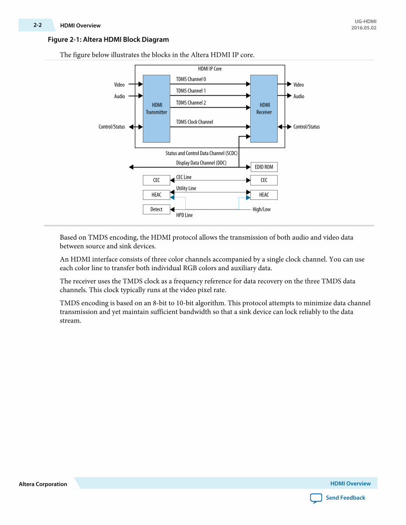
Figure 2-1: Altera HDMI Block Diagram
The figure below illustrates the blocks in the Altera HDMI IP core.
HDMITransmitter
HDMIReceiver
TDMS Channel 0
HDMI IP Core
TDMS Channel 1
TDMS Channel 2
TDMS Clock Channel
Video
Audio
Control/Status
Video
Audio
Control/Status
Detect
CEC
HEAC
EDID ROM
CEC
HEAC
CEC Line
Utility Line
HPD Line
Display Data Channel (DDC)
Status and Control Data Channel (SCDC)
High/Low
Based on TMDS encoding, the HDMI protocol allows the transmission of both audio and video databetween source and sink devices.
An HDMI interface consists of three color channels accompanied by a single clock channel. You can useeach color line to transfer both individual RGB colors and auxiliary data.
The receiver uses the TMDS clock as a frequency reference for data recovery on the three TMDS datachannels. This clock typically runs at the video pixel rate.
TMDS encoding is based on an 8-bit to 10-bit algorithm. This protocol attempts to minimize data channeltransmission and yet maintain sufficient bandwidth so that a sink device can lock reliably to the datastream.
2-2 HDMI OverviewUG-HDMI
2016.05.02
Altera Corporation HDMI Overview
Send Feedback
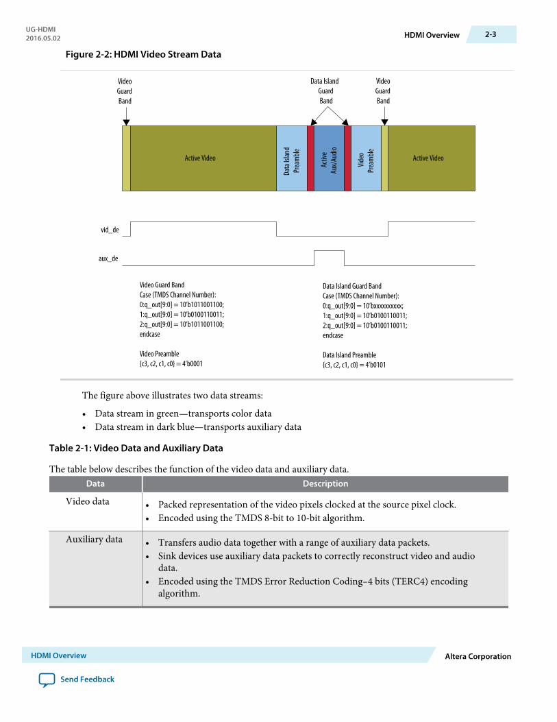
Figure 2-2: HDMI Video Stream Data
Active Video
Data
Islan
dPr
eam
ble
Activ
eAu
x/Au
dio
Video
Prea
mble Active Video
VideoGuardBand
VideoGuardBand
Data IslandGuardBand
vid_de
aux_de
Video Guard BandCase (TMDS Channel Number):0:q_out[9:0] = 10’b1011001100;1:q_out[9:0] = 10’b0100110011;2:q_out[9:0] = 10’b1011001100;endcase
Video Preamble{c3, c2, c1, c0} = 4’b0001
Data Island Guard BandCase (TMDS Channel Number):0:q_out[9:0] = 10’bxxxxxxxxxx;1:q_out[9:0] = 10’b0100110011;2:q_out[9:0] = 10’b0100110011;endcase
Data Island Preamble{c3, c2, c1, c0} = 4’b0101
The figure above illustrates two data streams:
• Data stream in green—transports color data• Data stream in dark blue—transports auxiliary data
Table 2-1: Video Data and Auxiliary Data
The table below describes the function of the video data and auxiliary data.Data Description
Video data • Packed representation of the video pixels clocked at the source pixel clock.• Encoded using the TMDS 8-bit to 10-bit algorithm.
Auxiliary data • Transfers audio data together with a range of auxiliary data packets.• Sink devices use auxiliary data packets to correctly reconstruct video and audio
data.• Encoded using the TMDS Error Reduction Coding–4 bits (TERC4) encoding
algorithm.
UG-HDMI2016.05.02 HDMI Overview 2-3
HDMI Overview Altera Corporation
Send Feedback
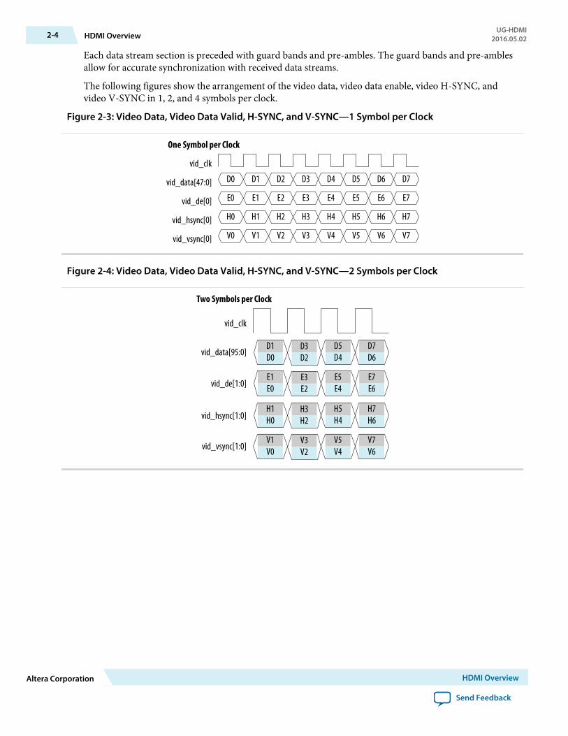
Each data stream section is preceded with guard bands and pre-ambles. The guard bands and pre-amblesallow for accurate synchronization with received data streams.
The following figures show the arrangement of the video data, video data enable, video H-SYNC, andvideo V-SYNC in 1, 2, and 4 symbols per clock.
Figure 2-3: Video Data, Video Data Valid, H-SYNC, and V-SYNC—1 Symbol per Clock
D0 D1 D2 D3 D4 D5 D6 D7
E0 E1 E2 E3 E4 E5 E6 E7
H0 H1 H2 H3 H4 H5 H6 H7
V0 V1 V2 V3 V4 V5 V6 V7
vid_clk
vid_data[47:0]
vid_de[0]
vid_hsync[0]
vid_vsync[0]
One Symbol per Clock
Figure 2-4: Video Data, Video Data Valid, H-SYNC, and V-SYNC—2 Symbols per Clock
vid_clk
vid_data[95:0]
vid_de[1:0]
vid_hsync[1:0]
vid_vsync[1:0]
Two Symbols per Clock
V1V0
V3V2
V5V4
V7V6
H1H0
H3H2
H5H4
H7H6
E1E0
E3E2
E5E4
E7E6
D1D0
D3D2
D5D4
D7D6
2-4 HDMI OverviewUG-HDMI
2016.05.02
Altera Corporation HDMI Overview
Send Feedback

Figure 2-5: Video Data, Video Data Valid, H-SYNC, and V-SYNC—4 Symbols per Clock
vid_clk
vid_data[191:0]
vid_de[3:0]
vid_hsync[3:0]
vid_vsync[3:0]
Four Symbols per Clock
V3V2V1V0
V7V6V5V4
H3H2H1H0
H7H6H5H4
E3E2E1E0
E7E6E5E4
D3D2D1D0
D7D6D5D4
Resource UtilizationThe resource utilization data indicates typical expected performance for the HDMI IP core device.
Table 2-2: HDMI Data Rate
The table lists the maximum data rates for HDMI core configurations of 1, 2, and 4 symbols per clock.
DevicesMaximum Data Rate (Mbps)
1 Symbol per Clock 2 Symbols per Clock 4 Symbols per Clock
Arria 10 Not Supported5,940
(Example: 4Kp60 8bpc)Not Supported
Arria V GX1,875
(Example: 1080p60 10bpc)
3,276.8
(Example: 4Kp30 8bpc)
5,940
(Example: 4Kp60 8bpc)
Stratix V5,800
(Example: 4Kp30 12bpc)
5,940
(Example: 4Kp60 8bpc)Not Supported
UG-HDMI2016.05.02 Resource Utilization 2-5
HDMI Overview Altera Corporation
Send Feedback
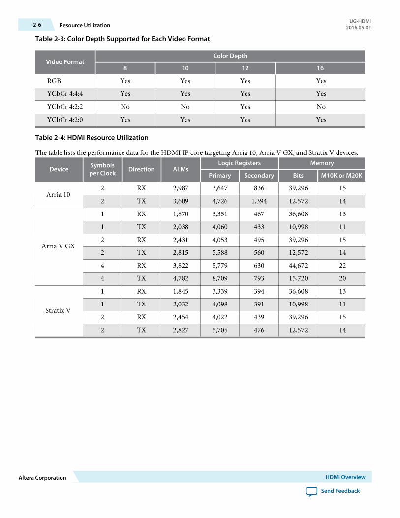
Table 2-3: Color Depth Supported for Each Video Format
Video FormatColor Depth
8 10 12 16
RGB Yes Yes Yes Yes
YCbCr 4:4:4 Yes Yes Yes Yes
YCbCr 4:2:2 No No Yes No
YCbCr 4:2:0 Yes Yes Yes Yes
Table 2-4: HDMI Resource Utilization
The table lists the performance data for the HDMI IP core targeting Arria 10, Arria V GX, and Stratix V devices.
Device Symbolsper Clock Direction ALMs
Logic Registers Memory
Primary Secondary Bits M10K or M20K
Arria 102 RX 2,987 3,647 836 39,296 15
2 TX 3,609 4,726 1,394 12,572 14
Arria V GX
1 RX 1,870 3,351 467 36,608 13
1 TX 2,038 4,060 433 10,998 11
2 RX 2,431 4,053 495 39,296 15
2 TX 2,815 5,588 560 12,572 14
4 RX 3,822 5,779 630 44,672 22
4 TX 4,782 8,709 793 15,720 20
Stratix V
1 RX 1,845 3,339 394 36,608 13
1 TX 2,032 4,098 391 10,998 11
2 RX 2,454 4,022 439 39,296 15
2 TX 2,827 5,705 476 12,572 14
2-6 Resource UtilizationUG-HDMI
2016.05.02
Altera Corporation HDMI Overview
Send Feedback

HDMI Getting Started 32016.05.02
UG-HDMI Subscribe Send Feedback
This chapter provides a general overview of the Altera IP core design flow to help you quickly get startedwith the HDMI IP core. The Altera IP Library is installed as part of the Quartus Prime installationprocess. You can select and parameterize any Altera IP core from the library. Altera provides anintegrated parameter editor that allows you to customize the HDMI IP core to support a wide variety ofapplications. The parameter editor guides you through the setting of parameter values and selection ofoptional ports.
Related Information
• Introduction to Altera IP CoresProvides general information about all Altera IP cores, including parameterizing, generating,upgrading, and simulating IP.
• Creating Version-Independent IP and Qsys Simulation ScriptsCreate simulation scripts that do not require manual updates for software or IP version upgrades.
• Project Management Best PracticesGuidelines for efficient management and portability of your project and IP files.
Installing and Licensing IP CoresThe Quartus Prime software includes the Altera IP Library. The library provides many useful IP corefunctions for production use without additional license. You can fully evaluate any licensed Altera IP corein simulation and in hardware until you are satisfied with its functionality and performance. The HDMIIP core is part of the Altera MegaCore IP Library, which is distributed with the Quartus Prime softwareand downloadable from the Altera web site.
Figure 3-1: HDMI Installation Path
Installation directory
ip - Contains the Altera IP Library
altera - Contains the Altera IP Library source code
altera_hdmi - Contains the HDMI IP core files
Note: The default IP installation directory on Windows is <drive>:\altera\<version number>; on Linux itis <home directory>/altera/ <version number>.
© 2016 Altera Corporation. All rights reserved. ALTERA, ARRIA, CYCLONE, ENPIRION, MAX, MEGACORE, NIOS, QUARTUS and STRATIX words and logos aretrademarks of Altera Corporation and registered in the U.S. Patent and Trademark Office and in other countries. All other words and logos identified astrademarks or service marks are the property of their respective holders as described at www.altera.com/common/legal.html. Altera warrants performanceof its semiconductor products to current specifications in accordance with Altera's standard warranty, but reserves the right to make changes to anyproducts and services at any time without notice. Altera assumes no responsibility or liability arising out of the application or use of any information,product, or service described herein except as expressly agreed to in writing by Altera. Altera customers are advised to obtain the latest version of devicespecifications before relying on any published information and before placing orders for products or services.
ISO9001:2008Registered
www.altera.com101 Innovation Drive, San Jose, CA 95134
After you purchase a license for the HDMI IP core, you can request a license file from the Altera'slicensing site and install it on your computer. When you request a license file, Altera emails you alicense.dat file. If you do not have Internet access, contact your local Altera representative.
Related Information
• Altera Licensing Site• Altera Software Installation and Licensing Manual
Specifying IP Core Parameters and OptionsFollow these steps to specify the HDMI IP core parameters and options.
1. Create a Quartus Prime project using the New Project Wizard available from the File menu.2. On the Tools menu, click IP Catalog.3. Under Installed IP, double-click Library > Interface > Protocols > Audio&Video > HDMI.
The parameter editor appears.4. Specify a top-level name for your custom IP variation. This name identifies the IP core variation files
in your project. If prompted, also specify the targeted Altera device family and output file HDLpreference. Click OK.
5. Specify parameters and options in the HDMI parameter editor:
• Optionally select preset parameter values. Presets specify all initial parameter values for specificapplications (where provided).
• Specify parameters defining the IP core functionality, port configurations, and device-specificfeatures.
• Specify options for generation of a timing netlist, simulation model, testbench, or example design(where applicable).
• Specify options for processing the IP core files in other EDA tools.6. Click Generate to generate the IP core and supporting files, including simulation models.7. Click Close when file generation completes.8. Click Finish.9. If you generate the HDMI IP core instance in a Quartus Prime project, you are prompted to add
Quartus Prime IP File (.qip) and Quartus Prime Simulation IP File (.sip) to the current Quartus Primeproject.
3-2 Specifying IP Core Parameters and OptionsUG-HDMI
2016.05.02
Altera Corporation HDMI Getting Started
Send Feedback
HDMI Source 42016.05.02
UG-HDMI Subscribe Send Feedback
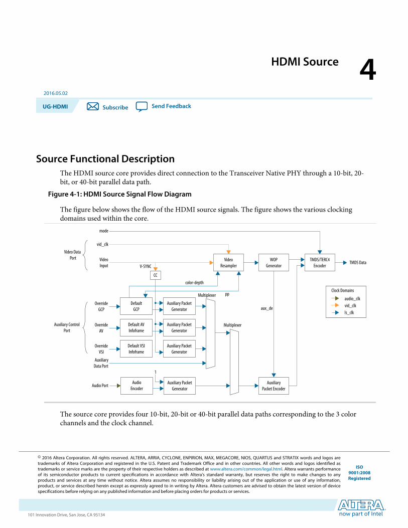
Source Functional DescriptionThe HDMI source core provides direct connection to the Transceiver Native PHY through a 10-bit, 20-bit, or 40-bit parallel data path.
Figure 4-1: HDMI Source Signal Flow Diagram
The figure below shows the flow of the HDMI source signals. The figure shows the various clockingdomains used within the core.
TMDS Data
audio_clkvid_clkls_clk
Clock Domains
TMDS/TERC4Encoder
WOPGenerator
VideoResampler
AuxiliaryPacket Encoder
Auxiliary PacketGenerator
Auxiliary PacketGenerator
Auxiliary PacketGenerator
CC
DefaultGCP
Default AVInfoframe
Default VSIInfoframe
Auxiliary PacketGenerator
mode
vid_clk
VideoInput
Override GCP
OverrideAV
OverrideVSI
AuxiliaryData Port
AudioEncoder
Audio Port
1
aux_de
color-depth
pp
V-SYNC
Video Data Port
Auxiliary ControlPort
Multiplexer
Multiplexer
The source core provides four 10-bit, 20-bit or 40-bit parallel data paths corresponding to the 3 colorchannels and the clock channel.
© 2016 Altera Corporation. All rights reserved. ALTERA, ARRIA, CYCLONE, ENPIRION, MAX, MEGACORE, NIOS, QUARTUS and STRATIX words and logos aretrademarks of Altera Corporation and registered in the U.S. Patent and Trademark Office and in other countries. All other words and logos identified astrademarks or service marks are the property of their respective holders as described at www.altera.com/common/legal.html. Altera warrants performanceof its semiconductor products to current specifications in accordance with Altera's standard warranty, but reserves the right to make changes to anyproducts and services at any time without notice. Altera assumes no responsibility or liability arising out of the application or use of any information,product, or service described herein except as expressly agreed to in writing by Altera. Altera customers are advised to obtain the latest version of devicespecifications before relying on any published information and before placing orders for products or services.
ISO9001:2008Registered
www.altera.com101 Innovation Drive, San Jose, CA 95134
The source core accepts video, audio, and auxiliary channel data streams. The core produces a TMDS/TERC4 encoded data stream that would typically connect to the high-speed transceiver parallel datainputs.
Central to the core is the TMDS/TERC4 encoder. The encoder processes either video or auxiliary data.
Source TMDS/TERC4 EncoderThe source TMDS/TERC4 encoder implements 8-bit to 10-bit and 4-bit to 10-bit algorithms as defined inthe HDMI Specification Ver.2.0. Each channel has its own encoder.
The encoder processes symbol data at 1, 2, or 4 symbols per clock.
When the encoder operates in 2 or 4 symbols per clock, it also produces the output in the form of two orfour encoded symbols per clock.
The TMDS/TERC4 encoder also produces digital visual interface (DVI) signaling when you deassert themode input signal. DVI signaling is identical to HDMI signaling, except for the absence of data and videoislands and TERC4 auxiliary data.
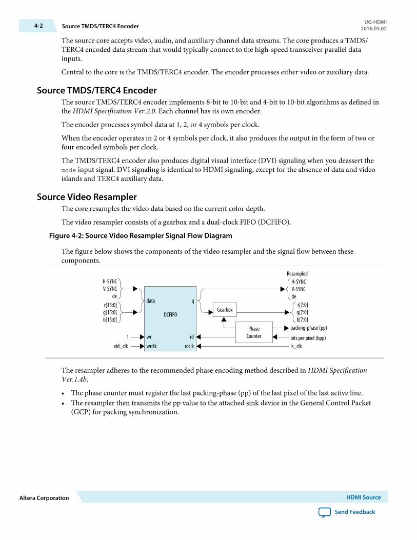
Source Video ResamplerThe core resamples the video data based on the current color depth.
The video resampler consists of a gearbox and a dual-clock FIFO (DCFIFO).
Figure 4-2: Source Video Resampler Signal Flow Diagram
The figure below shows the components of the video resampler and the signal flow between thesecomponents.
1
vid_clk
DCFIFO
ls_clk
data
wr
wrclk
q
rd
rdclk
de
H-SYNCV-SYNC
b[15:0]
r[15:0]g[15:0]
b[7:0]
r[7:0]g[7:0]
PhaseCounter
Gearbox
H-SYNCV-SYNCde
Resampled
packing-phase (pp)
bits per pixel (bpp)
The resampler adheres to the recommended phase encoding method described in HDMI SpecificationVer.1.4b.
• The phase counter must register the last packing-phase (pp) of the last pixel of the last active line.• The resampler then transmits the pp value to the attached sink device in the General Control Packet
(GCP) for packing synchronization.
4-2 Source TMDS/TERC4 EncoderUG-HDMI
2016.05.02
Altera Corporation HDMI Source
Send Feedback
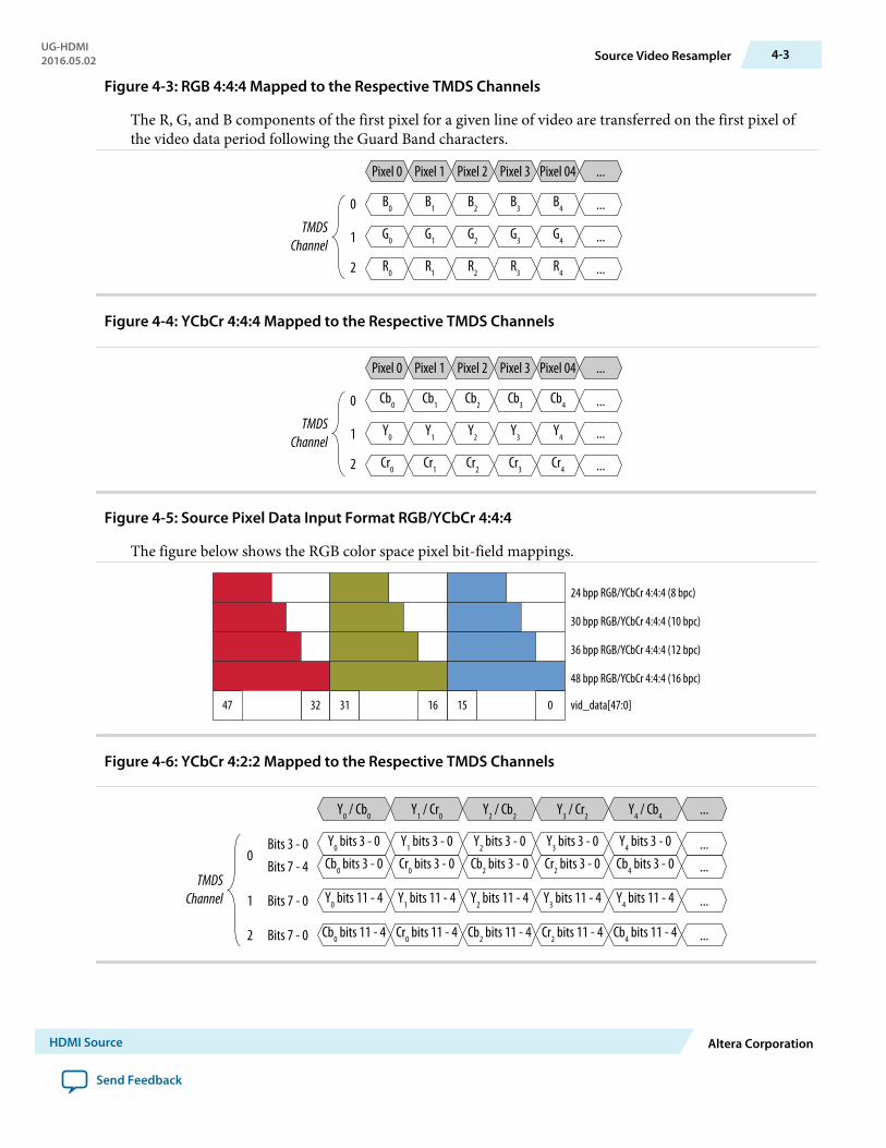
Figure 4-3: RGB 4:4:4 Mapped to the Respective TMDS Channels
The R, G, and B components of the first pixel for a given line of video are transferred on the first pixel ofthe video data period following the Guard Band characters.
Pixel 0 Pixel 1 Pixel 2 Pixel 3 Pixel 04
B0 B1 B2 B3 B4
TMDSChannel
0
1
2
G0 G1 G2 G3 G4
R0 R1 R2 R3 R4
...
...
...
...
Figure 4-4: YCbCr 4:4:4 Mapped to the Respective TMDS Channels
Pixel 0 Pixel 1 Pixel 2 Pixel 3 Pixel 04
Cb0 Cb1 Cb2 Cb3 Cb4
TMDSChannel
0
1
2
Y0 Y1 Y2 Y3 Y4
Cr0 Cr1 Cr2 Cr3 Cr4
...
...
...
...
Figure 4-5: Source Pixel Data Input Format RGB/YCbCr 4:4:4
The figure below shows the RGB color space pixel bit-field mappings.
47 32 31 16 15 0 vid_data[47:0]
24 bpp RGB/YCbCr 4:4:4 (8 bpc)
30 bpp RGB/YCbCr 4:4:4 (10 bpc)
36 bpp RGB/YCbCr 4:4:4 (12 bpc)
48 bpp RGB/YCbCr 4:4:4 (16 bpc)
Figure 4-6: YCbCr 4:2:2 Mapped to the Respective TMDS Channels
Y0 / Cb0 Y1 / Cr0 Y2 / Cb2 Y3 / Cr2 Y4 / Cb4
TMDSChannel
0
1
2
Y0 bits 3 - 0 Y1 bits 3 - 0 Y2 bits 3 - 0 Y3 bits 3 - 0 Y4 bits 3 - 0
...
...Cb0 bits 3 - 0 Cr0 bits 3 - 0 Cb2 bits 3 - 0 Cr2 bits 3 - 0 Cb4 bits 3 - 0 ...
Y0 bits 11 - 4 Y1 bits 11 - 4 Y2 bits 11 - 4 Y3 bits 11 - 4 Y4 bits 11 - 4 ...
Bits 3 - 0
Bits 7 - 4
Bits 7 - 0
Cb0 bits 11 - 4 Cr0 bits 11 - 4 Cb2 bits 11 - 4 Cr2 bits 11 - 4 Cb4 bits 11 - 4 ...Bits 7 - 0
UG-HDMI2016.05.02 Source Video Resampler 4-3
HDMI Source Altera Corporation
Send Feedback
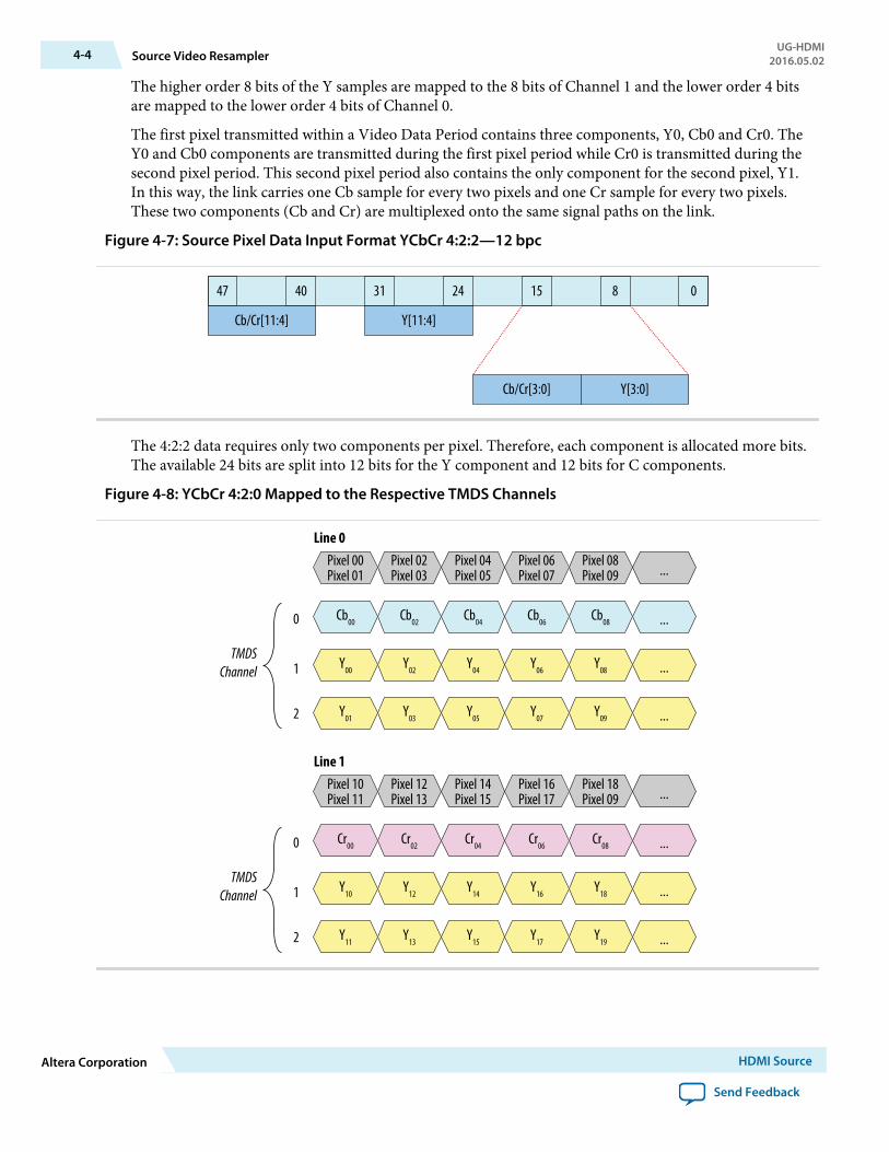
The higher order 8 bits of the Y samples are mapped to the 8 bits of Channel 1 and the lower order 4 bitsare mapped to the lower order 4 bits of Channel 0.
The first pixel transmitted within a Video Data Period contains three components, Y0, Cb0 and Cr0. TheY0 and Cb0 components are transmitted during the first pixel period while Cr0 is transmitted during thesecond pixel period. This second pixel period also contains the only component for the second pixel, Y1.In this way, the link carries one Cb sample for every two pixels and one Cr sample for every two pixels.These two components (Cb and Cr) are multiplexed onto the same signal paths on the link.
Figure 4-7: Source Pixel Data Input Format YCbCr 4:2:2—12 bpc
47 40 31 24 15 8 0
Cb/Cr[11:4] Y[11:4]
Cb/Cr[3:0] Y[3:0]
The 4:2:2 data requires only two components per pixel. Therefore, each component is allocated more bits.The available 24 bits are split into 12 bits for the Y component and 12 bits for C components.
Figure 4-8: YCbCr 4:2:0 Mapped to the Respective TMDS Channels
Pixel 00Pixel 01
Cb00 Cb02 Cb04 Cb06 Cb08
TMDSChannel
0
1
2
Y00 Y02 Y04 Y06 Y08
Y01 Y03 Y05 Y07 Y09
...
...
...
...
Pixel 02Pixel 03
Pixel 04Pixel 05
Pixel 06Pixel 07
Pixel 08Pixel 09
Line 0
Pixel 10Pixel 11
Cr00 Cr02 Cr04 Cr06 Cr08
TMDSChannel
0
1
2
Y10 Y12 Y14 Y16 Y18
Y11 Y13 Y15 Y17 Y19
...
...
...
...
Pixel 12Pixel 13
Pixel 14Pixel 15
Pixel 16Pixel 17
Pixel 18Pixel 09
Line 1
4-4 Source Video ResamplerUG-HDMI
2016.05.02
Altera Corporation HDMI Source
Send Feedback

The two horizontally succesive 8-bit Y components are transmitted in TMDS Channels 1 and 2, in thatorder. The 8-bit Cb or Cr components are transmitted alternately in TMDS Channel 0, line by line.
Mapping Formats
The following figures illustrate the mapping of different formats.
Figure 4-9: Mapping Two 8-Bit per Component YCbCr 4:2:0 to One 24-Bit YCbCr 4:4:4 Pixel (Pre DeepColor Packing)
Channel 0
Channel 1
Channel 2
Channel 0
Channel 1
Channel 2
Channel 0
Channel 1
Channel 2
Channel 0
Channel 1
Channel 2
Cb00[7:0]
Y00[7:0]
Y01[7:0]
Cr00[7:0]
Y10[7:0]
Y11[7:0]
Cb20[7:0]
Y20[7:0]
Y21[7:0]
Cr20[7:0]
Y30[7:0]
Y31[7:0]
Cb[7:0]
Y[7:0]
Cr[7:0]
Cb[7:0]
Y[7:0]
Cr[7:0]
Cb[7:0]
Y[7:0]
Cr[7:0]
Cb[7:0]
Y[7:0]
Cr[7:0]
Cb02[7:0]
Y02[7:0]
Y03[7:0]
Cr02[7:0]
Y12[7:0]
Y13[7:0]
Cb22[7:0]
Y22[7:0]
Y23[7:0]
Cr22[7:0]
Y32[7:0]
Y33[7:0]
Cb04[7:0]
Y04[7:0]
Y05[7:0]
Cr04[7:0]
Y14[7:0]
Y15[7:0]
Cb24[7:0]
Y24[7:0]
Y25[7:0]
Cr24[7:0]
Y34[7:0]
Y35[7:0]
Cb06[7:0]
Y06[7:0]
Y07[7:0]
Cr06[7:0]
Y16[7:0]
Y17[7:0]
Cb26[7:0]
Y26[7:0]
Y27[7:0]
Cr26[7:0]
Y36[7:0]
Y37[7:0]
EquivalentYCbCr 4:4:4 Pixel
YCbCr 4:2:0Pixel 0/1
YCbCr 4:2:0Pixel 2/3
YCbCr 4:2:0Pixel 4/5
YCbCr 4:2:0Pixel 6/7
Line 0
Line 1
Line 2
Line 3
First 8 YCbCr 4:2:0 Pixels on Each Line
UG-HDMI2016.05.02 Mapping Formats 4-5
HDMI Source Altera Corporation
Send Feedback

Figure 4-10: Mapping Two 10-Bit per Component YCbCr 4:2:0 to One 30-Bit YCbCr 4:4:4 Pixel (Pre DeepColor Packing)
Channel 0
Channel 1
Channel 2
Channel 0
Channel 1
Channel 2
Channel 0
Channel 1
Channel 2
Channel 0
Channel 1
Channel 2
Cb00[9:0]
Y00[9:0]
Y01[9:0]
Cr00[9:0]
Y10[9:0]
Y11[9:0]
Cb20[9:0]
Y20[9:0]
Y21[9:0]
Cr20[9:0]
Y30[9:0]
Y31[9:0]
Cb[9:0]
Y[9:0]
Cr[9:0]
Cb[9:0]
Y[9:0]
Cr[9:0]
Cb[9:0]
Y[9:0]
Cr[9:0]
Cb[9:0]
Y[9:0]
Cr[9:0]
Cb02[9:0]
Y02[9:0]
Y03[9:0]
Cr02[9:0]
Y12[9:0]
Y13[9:0]
Cb22[9:0]
Y22[9:0]
Y23[9:0]
Cr22[9:0]
Y32[9:0]
Y33[9:0]
Cb04[9:0]
Y04[9:0]
Y05[9:0]
Cr04[9:0]
Y14[9:0]
Y15[9:0]
Cb24[9:0]
Y24[9:0]
Y25[9:0]
Cr24[9:0]
Y34[9:0]
Y35[9:0]
Cb06[9:0]
Y06[9:0]
Y07[9:0]
Cr06[9:0]
Y16[9:0]
Y17[9:0]
Cb26[9:0]
Y26[9:0]
Y27[9:0]
Cr26[9:0]
Y36[9:0]
Y37[9:0]
EquivalentYCbCr 4:4:4 Pixel
YCbCr 4:2:0Pixel 0/1
YCbCr 4:2:0Pixel 2/3
YCbCr 4:2:0Pixel 4/5
YCbCr 4:2:0Pixel 6/7
Line 0
Line 1
Line 2
Line 3
First 10 YCbCr 4:2:0 Pixels on Each Line
Figure 4-11: Mapping Two 12-Bit per Component YCbCr 4:2:0 to One 36-Bit YCbCr 4:4:4 Pixel (Pre DeepColor Packing)
Channel 0
Channel 1
Channel 2
Channel 0
Channel 1
Channel 2
Channel 0
Channel 1
Channel 2
Channel 0
Channel 1
Channel 2
Cb00[11:0]
Y00[11:0]
Y01[11:0]
Cr00[11:0]
Y10[11:0]
Y11[11:0]
Cb20[11:0]
Y20[11:0]
Y21[11:0]
Cr20[11:0]
Y30[11:0]
Y31[11:0]
Cb[11:0]
Y[11:0]
Cr[11:0]
Cb[11:0]
Y[11:0]
Cr[11:0]
Cb[11:0]
Y[11:0]
Cr[11:0]
Cb[11:0]
Y[11:0]
Cr[11:0]
Cb02[11:0]
Y02[11:0]
Y03[11:0]
Cr02[11:0]
Y12[11:0]
Y13[11:0]
Cb22[11:0]
Y22[11:0]
Y23[11:0]
Cr22[11:0]
Y32[11:0]
Y33[11:0]
Cb04[11:0]
Y04[11:0]
Y05[11:0]
Cr04[11:0]
Y14[11:0]
Y15[11:0]
Cb24[11:0]
Y24[11:0]
Y25[11:0]
Cr24[11:0]
Y34[11:0]
Y35[11:0]
Cb06[11:0]
Y06[11:0]
Y07[11:0]
Cr06[11:0]
Y16[11:0]
Y17[11:0]
Cb26[11:0]
Y26[11:0]
Y27[11:0]
Cr26[11:0]
Y36[11:0]
Y37[11:0]
EquivalentYCbCr 4:4:4 Pixel
YCbCr 4:2:0Pixel 0/1
YCbCr 4:2:0Pixel 2/3
YCbCr 4:2:0Pixel 4/5
YCbCr 4:2:0Pixel 6/7
Line 0
Line 1
Line 2
Line 3
First 12 YCbCr 4:2:0 Pixels on Each Line
4-6 Mapping FormatsUG-HDMI
2016.05.02
Altera Corporation HDMI Source
Send Feedback
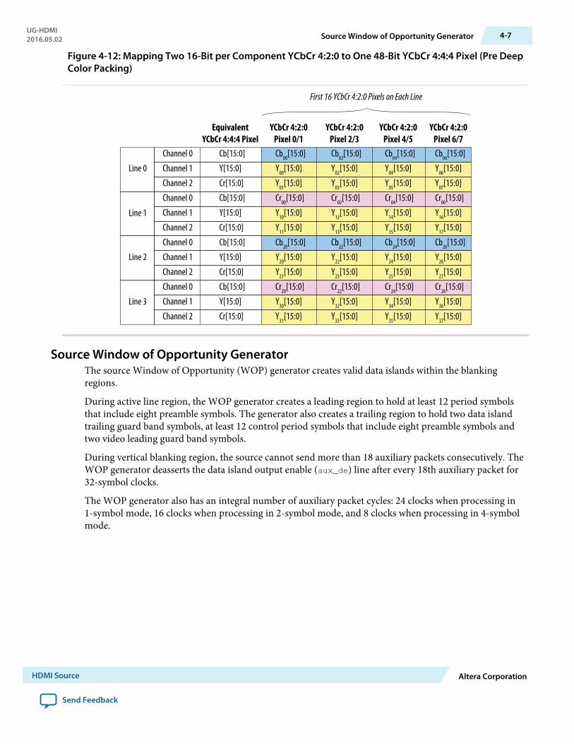
Figure 4-12: Mapping Two 16-Bit per Component YCbCr 4:2:0 to One 48-Bit YCbCr 4:4:4 Pixel (Pre DeepColor Packing)
Channel 0
Channel 1
Channel 2
Channel 0
Channel 1
Channel 2
Channel 0
Channel 1
Channel 2
Channel 0
Channel 1
Channel 2
Cb00[15:0]
Y00[15:0]
Y01[15:0]
Cr00[15:0]
Y10[15:0]
Y11[15:0]
Cb20[15:0]
Y20[15:0]
Y21[15:0]
Cr20[15:0]
Y30[15:0]
Y31[15:0]
Cb[15:0]
Y[15:0]
Cr[15:0]
Cb[15:0]
Y[15:0]
Cr[15:0]
Cb[15:0]
Y[15:0]
Cr[15:0]
Cb[15:0]
Y[15:0]
Cr[15:0]
Cb02[15:0]
Y02[15:0]
Y03[15:0]
Cr02[15:0]
Y12[15:0]
Y13[15:0]
Cb22[15:0]
Y22[15:0]
Y23[15:0]
Cr22[15:0]
Y32[15:0]
Y33[15:0]
Cb04[15:0]
Y04[15:0]
Y05[15:0]
Cr04[15:0]
Y14[15:0]
Y15[15:0]
Cb24[15:0]
Y24[15:0]
Y25[15:0]
Cr24[15:0]
Y34[15:0]
Y35[15:0]
Cb06[15:0]
Y06[15:0]
Y07[15:0]
Cr06[15:0]
Y16[15:0]
Y17[15:0]
Cb26[15:0]
Y26[15:0]
Y27[15:0]
Cr26[15:0]
Y36[15:0]
Y37[15:0]
EquivalentYCbCr 4:4:4 Pixel
YCbCr 4:2:0Pixel 0/1
YCbCr 4:2:0Pixel 2/3
YCbCr 4:2:0Pixel 4/5
YCbCr 4:2:0Pixel 6/7
Line 0
Line 1
Line 2
Line 3
First 16 YCbCr 4:2:0 Pixels on Each Line
Source Window of Opportunity GeneratorThe source Window of Opportunity (WOP) generator creates valid data islands within the blankingregions.
During active line region, the WOP generator creates a leading region to hold at least 12 period symbolsthat include eight preamble symbols. The generator also creates a trailing region to hold two data islandtrailing guard band symbols, at least 12 control period symbols that include eight preamble symbols andtwo video leading guard band symbols.
During vertical blanking region, the source cannot send more than 18 auxiliary packets consecutively. TheWOP generator deasserts the data island output enable (aux_de) line after every 18th auxiliary packet for32-symbol clocks.
The WOP generator also has an integral number of auxiliary packet cycles: 24 clocks when processing in1-symbol mode, 16 clocks when processing in 2-symbol mode, and 8 clocks when processing in 4-symbolmode.
UG-HDMI2016.05.02 Source Window of Opportunity Generator 4-7
HDMI Source Altera Corporation
Send Feedback
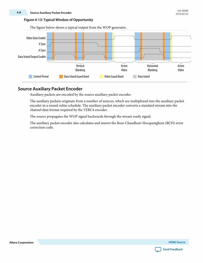
Figure 4-13: Typical Window of Opportunity
The figure below shows a typical output from the WOP generator.
Video Data Enable
V Sync
H Sync
Data Island Output Enable
VerticalBlanking
ActiveVideo
HorizontalBlanking
ActiveVideo
Control Period Data Island Guard Band Video Guard Band Data Island
Source Auxiliary Packet EncoderAuxiliary packets are encoded by the source auxiliary packet encoder.
The auxiliary packets originate from a number of sources, which are multiplexed into the auxiliary packetencoder in a round-robin schedule. The auxiliary packet encoder converts a standard stream into thechannel data format required by the TERC4 encoder.
The source propagates the WOP signal backwards through the stream ready signal.
The auxiliary packet encoder also calculates and inserts the Bose-Chaudhuri-Hocquenghem (BCH) errorcorrection code.
4-8 Source Auxiliary Packet EncoderUG-HDMI
2016.05.02
Altera Corporation HDMI Source
Send Feedback

Figure 4-14: Auxiliary Packet Encoder Input
The figure below shows the auxiliary packet encoder input from a 72-bit input data.
PB22
PB21
PB15
PB14
PB8
PB7
PB1
PB0
HB0
Phase 0
PB24
PB23
PB17
PB16
PB10
PB9
PB3
PB2
HB1
Phase 1
PB26
PB25
PB19
PB18
PB12
PB11
PB5
PB4
HB2
Phase 2
0
PB27
0
PB20
0
PB13
0
PB6
0
Phase 3
BCH Block 3
BCH Block 2
BCH Block 1
BCH Block 0
Input Data
Byte[8]
Byte[0]
Startofpacket
Endofpacket
Ready
Clock
0 - - 8 - - 16 - - 24Cycle 1 Symbol
0 - - 4 - - 8 - - 12Cycle 2 Symbol
0 - - 2 - - 4 - - 6Cycle 4 Symbol
Phase 0 Phase 1 Phase 2 Phase 3
The encoder assumes the data valid input will remain asserted for the duration of a packet to complete. Apacket is always 24 clocks (in 1-symbol mode), 12 clocks (in 2-symbol mode), or 6 clocks (in 4-symbolmode).
The encoder creates a NULL auxiliary packet if it doesn't detect a start-of-packet at the beginning of apacket boundary. In this case, you can consider the output of the encoder as a stream of NULL packetsunless a valid packet is available.
UG-HDMI2016.05.02 Source Auxiliary Packet Encoder 4-9
HDMI Source Altera Corporation
Send Feedback

Figure 4-15: Typical Auxiliary Packet Stream During Blanking Interval
The figure below shows a typical auxiliary packet stream in 1-symbol per clock mode, where 0 denotes anull packet.
wop
0 0 0 0 AVI 0 AI VSI 0 0 0
0 23 47 71
Auxiliary Packet
Clock Cycle
AVI = Auxiliary Video InfoframeAI = Audio Information InfoframeVSI = Vendor Specific Infoframe
.......
Ninth PacketSkipped
Source Auxiliary Packet GeneratorsThe source core uses various auxiliary packet generators. The packet generators convert the packet fieldinputs to the auxiliary packet stream format.
The packet generator propagates backpressure from the output ready signal to the input ready signal. Thegenerator asserts the input valid signal when a packet is ready to be transmitted. The input valid signalremains asserted until the generator receives a ready acknowledgment.
Source Auxiliary Data Path MultiplexersThe auxiliary data path multiplexers provide paths for the various auxiliary packet generators.
The various auxiliary packet generators traverse a multiplexed routing path to the auxiliary packetencoder. The multiplexers obey a round-robin schedule and propagate backpressure.
Source Auxiliary Control PortTo simplify the user logic, the source core has control ports to send the most common auxiliary controlpackets.
These packets are: General Control Packet, Auxiliary Video Information (AVI) InfoFrame, HDMIVendor Specific InfoFrame (VSI), and Audio InfoFrame.
The core sends the default values in the auxiliary packets. The default values allow the core to send videodata compatible with the HDMI Specification Ver.1.4b with minimum description.
You can also override the generators using the customized input values. The override values replace thedefault values when the input checksum is non-zero.
The core sends the auxiliary control packets on the active edge of the V-SYNC signal to ensure that thepackets are sent once per field.
4-10 Source Auxiliary Packet GeneratorsUG-HDMI
2016.05.02
Altera Corporation HDMI Source
Send Feedback
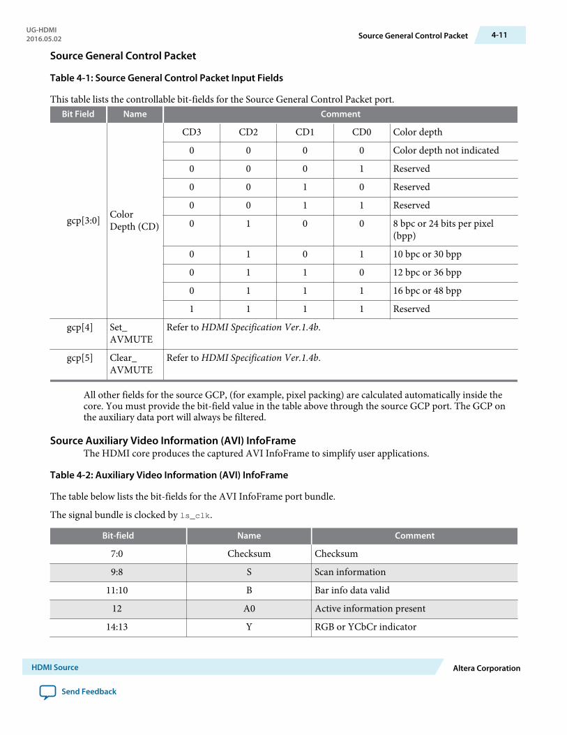
Source General Control Packet
Table 4-1: Source General Control Packet Input Fields
This table lists the controllable bit-fields for the Source General Control Packet port.Bit Field Name Comment
gcp[3:0] ColorDepth (CD)
CD3 CD2 CD1 CD0 Color depth
0 0 0 0 Color depth not indicated
0 0 0 1 Reserved
0 0 1 0 Reserved
0 0 1 1 Reserved
0 1 0 0 8 bpc or 24 bits per pixel(bpp)
0 1 0 1 10 bpc or 30 bpp
0 1 1 0 12 bpc or 36 bpp
0 1 1 1 16 bpc or 48 bpp
1 1 1 1 Reserved
gcp[4] Set_AVMUTE
Refer to HDMI Specification Ver.1.4b.
gcp[5] Clear_AVMUTE
Refer to HDMI Specification Ver.1.4b.
All other fields for the source GCP, (for example, pixel packing) are calculated automatically inside thecore. You must provide the bit-field value in the table above through the source GCP port. The GCP onthe auxiliary data port will always be filtered.
Source Auxiliary Video Information (AVI) InfoFrameThe HDMI core produces the captured AVI InfoFrame to simplify user applications.
Table 4-2: Auxiliary Video Information (AVI) InfoFrame
The table below lists the bit-fields for the AVI InfoFrame port bundle.
The signal bundle is clocked by ls_clk.
Bit-field Name Comment
7:0 Checksum Checksum
9:8 S Scan information
11:10 B Bar info data valid
12 A0 Active information present
14:13 Y RGB or YCbCr indicator
UG-HDMI2016.05.02 Source General Control Packet 4-11
HDMI Source Altera Corporation
Send Feedback

Bit-field Name Comment
15 Reserved Returns 0
19:16 R Active format aspect ratio
21:20 M Picture aspect ratio
23:22 C Colorimetry (for example: ITU BT.601, BT.709)
25:24 SC Non-uniform picture scaling
27:26 Q Quantization range
30:28 EC Extended colorimetry
31 ITC IT content
38:32 VIC Video format identification code
39 Reserved Returns 0
43:40 PR Picture repetition factor
45:44 CN Content type
47:46 YQ YCC quantization range
63:48 ETB Line number of end of top bar
79:64 SBB Line number of start of bottom bar
95:80 ELB Pixel number of end of left bar
111:96 SRB Pixel number of start of right bar
112 Control Disables the core from inserting theInfoFrame packet.
• 1: The core does not insert info_avi[111:0]. The AVI InfoFrame packeton the auxiliary data port passes through.
• 0: The core inserts info_avi[111:0]when checksum field (info_avi[7:0]) isnon-zero. The core sends default valueswhen checksum field (info_avi[7:0]) iszero. The core filters the AVI InfoFramepacket on the auxiliary data port.
Source HDMI Vendor Specific InfoFrame (VSI)The core transmits a HDMI Vendor Specific InfoFrame once per field.
4-12 Source HDMI Vendor Specific InfoFrame (VSI)UG-HDMI
2016.05.02
Altera Corporation HDMI Source
Send Feedback
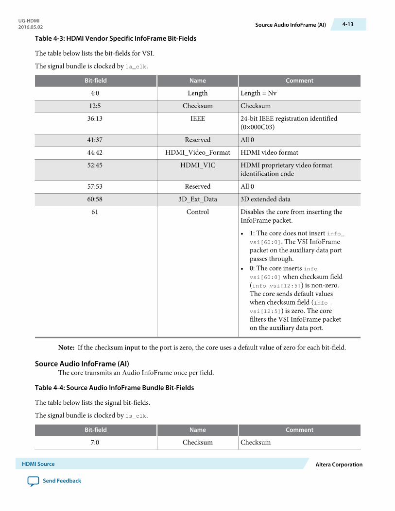
Table 4-3: HDMI Vendor Specific InfoFrame Bit-Fields
The table below lists the bit-fields for VSI.
The signal bundle is clocked by ls_clk.
Bit-field Name Comment
4:0 Length Length = Nv
12:5 Checksum Checksum
36:13 IEEE 24-bit IEEE registration identified(0×000C03)
41:37 Reserved All 0
44:42 HDMI_Video_Format HDMI video format
52:45 HDMI_VIC HDMI proprietary video formatidentification code
57:53 Reserved All 0
60:58 3D_Ext_Data 3D extended data
61 Control Disables the core from inserting theInfoFrame packet.
• 1: The core does not insert info_vsi[60:0]. The VSI InfoFramepacket on the auxiliary data portpasses through.
• 0: The core inserts info_vsi[60:0] when checksum field(info_vsi[12:5]) is non-zero.The core sends default valueswhen checksum field (info_vsi[12:5]) is zero. The corefilters the VSI InfoFrame packeton the auxiliary data port.
Note: If the checksum input to the port is zero, the core uses a default value of zero for each bit-field.
Source Audio InfoFrame (AI)The core transmits an Audio InfoFrame once per field.
Table 4-4: Source Audio InfoFrame Bundle Bit-Fields
The table below lists the signal bit-fields.
The signal bundle is clocked by ls_clk.
Bit-field Name Comment
7:0 Checksum Checksum
UG-HDMI2016.05.02 Source Audio InfoFrame (AI) 4-13
HDMI Source Altera Corporation
Send Feedback
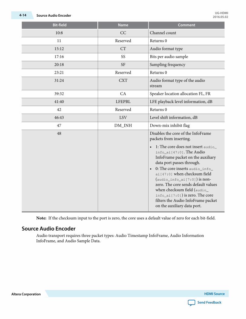
Bit-field Name Comment
10:8 CC Channel count
11 Reserved Returns 0
15:12 CT Audio format type
17:16 SS Bits per audio sample
20:18 SF Sampling frequency
23:21 Reserved Returns 0
31:24 CXT Audio format type of the audiostream
39:32 CA Speaker location allocation FL, FR
41:40 LFEPBL LFE playback level information, dB
42 Reserved Returns 0
46:43 LSV Level shift information, dB
47 DM_INH Down-mix inhibit flag
48 Disables the core of the InfoFramepackets from inserting.
• 1: The core does not insert audio_info_ai[47:0]. The AudioInfoFrame packet on the auxiliarydata port passes through.
• 0: The core inserts audio_info_ai[47:0] when checksum field(audio_info_ai[7:0]) is non-zero. The core sends default valueswhen checksum field (audio_info_ai[7:0]) is zero. The corefilters the Audio InfoFrame packeton the auxiliary data port.
Note: If the checksum input to the port is zero, the core uses a default value of zero for each bit-field.
Source Audio EncoderAudio transport requires three packet types: Audio Timestamp InfoFrame, Audio InformationInfoFrame, and Audio Sample Data.
4-14 Source Audio EncoderUG-HDMI
2016.05.02
Altera Corporation HDMI Source
Send Feedback
Figure 4-16: Source Audio Encoder
TimestampScheduler
Auxiliary PacketGenerator
Auxiliary PacketGenerator
Audio Format
Default AIV-SYNC
1
Auxiliary PacketGenerator
AudioPacketizer
DCFIFO
Auxiliary PacketGenerator
CTS, N
Default AI
Audio Input
Audio Metadata
Multiplexer
AudioAuxiliaryStream
Audio Data Port
The Audio Timestamp InfoFrame packet contains the CTS and N values. You need to provide thesevalues. The core schedules this packet to be sent every ms. The scheduler uses the audio_clk and N valueto determine a 1-ms interval.
The core sends the Audio Information InfoFrame packet on the active edge of the V-SYNC signal.
The Audio Sample Data packet queues on a DCFIFO. The core also uses the DCFIFO to synchronize itsclock to ls_clk. The Audio Packetizer packs the audio sample data into the Audio Sample packetsaccording to the specified audio format. An Audio Sample packet can contain up to 4 audio samples,based on the required audio sample clock. The core sends the Audio Sample packets whenever there is anavailable slot in the auxiliary packet stream.
The audio_data port is always at a fixed 256 bits and the audio_de port is always fixed at 8 bits. Foraudio channels fewer than 8, the DispayPort source pads the most significant bits with 0s.
The 32-bit audio data is packed in IEC-60958 standard. The least significant word is the left channelsample.
Figure 4-17: Audio Data Packing
SP x x B P C U V Audio Data
31
The fields are defined as:
SPxBPCUV
: Sample Present: Not Used: Start of 192-bit IEC-60958 Channel Status: Parity Bit: Channel Status: User Data Bit: Valid Bit
24 0
UG-HDMI2016.05.02 Source Audio Encoder 4-15
HDMI Source Altera Corporation
Send Feedback
The Audio Timestamp InfoFrame and Audio Sample Data packets on the Auxiliary Data Port are notfiltered by the source. You must filter these packets externally if you want to loop back the auxiliary datastream from the sink. The Audio Information InfoFrame packet on the Auxiliary Data Port will be filteredby the source if the most significant bit of audio_info_ai port is set to 0.
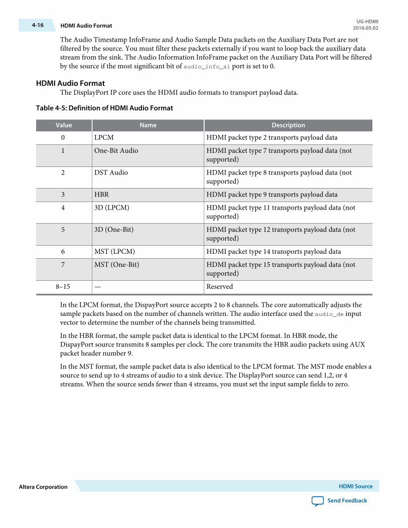
HDMI Audio FormatThe DisplayPort IP core uses the HDMI audio formats to transport payload data.
Table 4-5: Definition of HDMI Audio Format
Value Name Description
0 LPCM HDMI packet type 2 transports payload data
1 One-Bit Audio HDMI packet type 7 transports payload data (notsupported)
2 DST Audio HDMI packet type 8 transports payload data (notsupported)
3 HBR HDMI packet type 9 transports payload data
4 3D (LPCM) HDMI packet type 11 transports payload data (notsupported)
5 3D (One-Bit) HDMI packet type 12 transports payload data (notsupported)
6 MST (LPCM) HDMI packet type 14 transports payload data
7 MST (One-Bit) HDMI packet type 15 transports payload data (notsupported)
8–15 — Reserved
In the LPCM format, the DispayPort source accepts 2 to 8 channels. The core automatically adjusts thesample packets based on the number of channels written. The audio interface used the audio_de inputvector to determine the number of the channels being transmitted.
In the HBR format, the sample packet data is identical to the LPCM format. In HBR mode, theDispayPort source transmits 8 samples per clock. The core transmits the HBR audio packets using AUXpacket header number 9.
In the MST format, the sample packet data is also identical to the LPCM format. The MST mode enables asource to send up to 4 streams of audio to a sink device. The DisplayPort source can send 1,2, or 4streams. When the source sends fewer than 4 streams, you must set the input sample fields to zero.
4-16 HDMI Audio FormatUG-HDMI
2016.05.02
Altera Corporation HDMI Source
Send Feedback
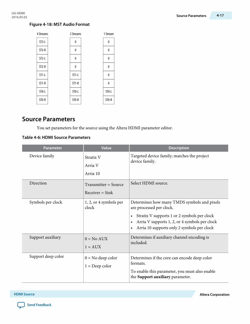
Figure 4-18: MST Audio Format
ST3-L
ST3-R
ST2-L
ST2-R
ST1-L
ST1-R
ST0-L
ST0-R
4 Streams
0
0
0
0
ST1-L
ST1-R
ST0-L
ST0-R
2 Streams
0
0
0
0
0
0
ST0-L
ST0-R
1 Stream
Source ParametersYou set parameters for the source using the Altera HDMI parameter editor.
Table 4-6: HDMI Source Parameters
Parameter Value Description
Device family Stratix V
Arria V
Arria 10
Targeted device family; matches the projectdevice family.
Direction Transmitter = Source
Receiver = Sink
Select HDMI source.
Symbols per clock 1, 2, or 4 symbols perclock
Determines how many TMDS symbols and pixelsare processed per clock.
• Stratix V supports 1 or 2 symbols per clock• Arria V supports 1, 2, or 4 symbols per clock• Arria 10 supports only 2 symbols per clock
Support auxiliary 0 = No AUX
1 = AUX
Determines if auxiliary channel encoding isincluded.
Support deep color 0 = No deep color
1 = Deep color
Determines if the core can encode deep colorformats.
To enable this parameter, you must also enablethe Support auxiliary parameter.
UG-HDMI2016.05.02 Source Parameters 4-17
HDMI Source Altera Corporation
Send Feedback
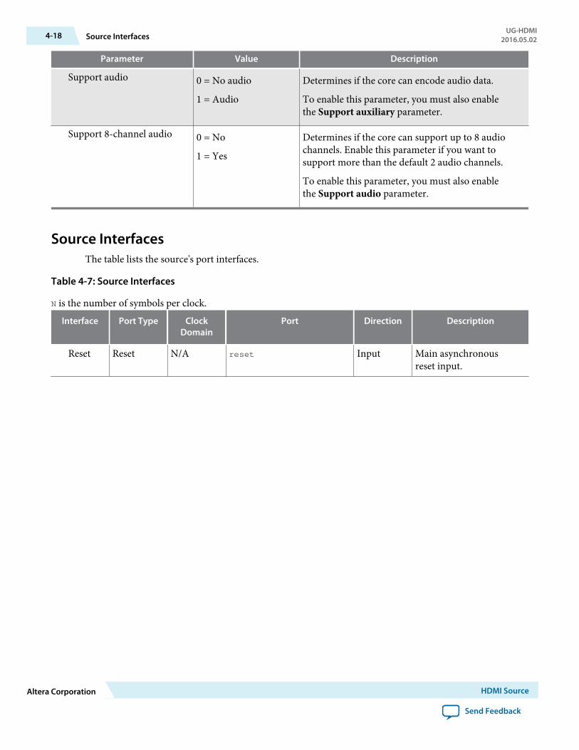
Parameter Value Description
Support audio 0 = No audio
1 = Audio
Determines if the core can encode audio data.
To enable this parameter, you must also enablethe Support auxiliary parameter.
Support 8-channel audio 0 = No
1 = Yes
Determines if the core can support up to 8 audiochannels. Enable this parameter if you want tosupport more than the default 2 audio channels.
To enable this parameter, you must also enablethe Support audio parameter.
Source InterfacesThe table lists the source's port interfaces.
Table 4-7: Source Interfaces
N is the number of symbols per clock.
Interface Port Type ClockDomain
Port Direction Description
Reset Reset N/A reset Input Main asynchronousreset input.
4-18 Source InterfacesUG-HDMI
2016.05.02
Altera Corporation HDMI Source
Send Feedback
Interface Port Type ClockDomain
Port Direction Description
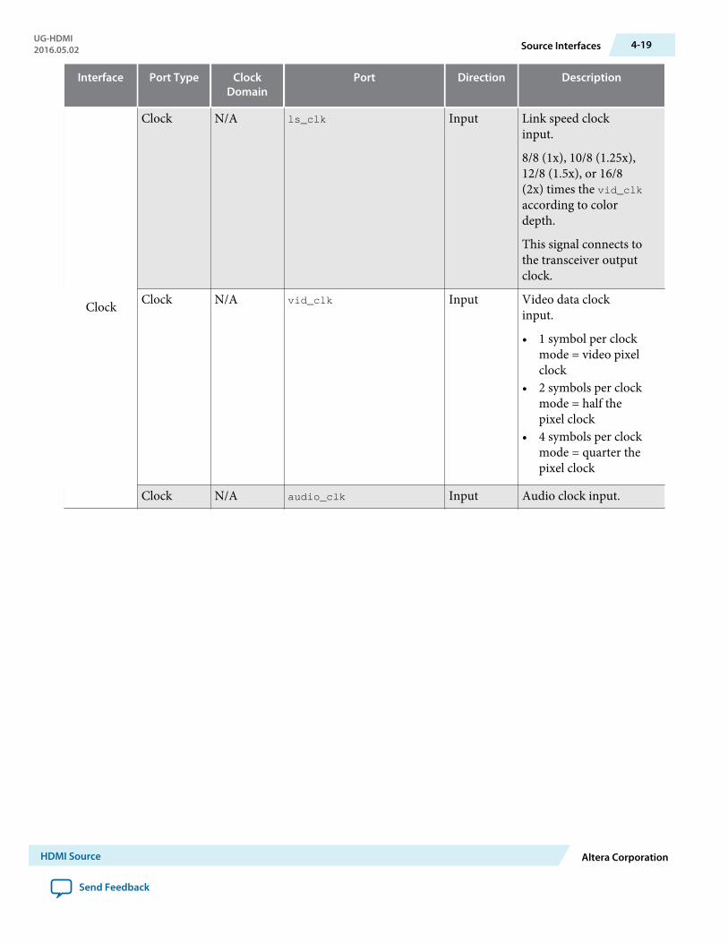
Clock
Clock N/A ls_clk Input Link speed clockinput.
8/8 (1x), 10/8 (1.25x),12/8 (1.5x), or 16/8(2x) times the vid_clkaccording to colordepth.
This signal connects tothe transceiver outputclock.
Clock N/A vid_clk Input Video data clockinput.
• 1 symbol per clockmode = video pixelclock
• 2 symbols per clockmode = half thepixel clock
• 4 symbols per clockmode = quarter thepixel clock
Clock N/A audio_clk Input Audio clock input.
UG-HDMI2016.05.02 Source Interfaces 4-19
HDMI Source Altera Corporation
Send Feedback
Interface Port Type ClockDomain
Port Direction Description
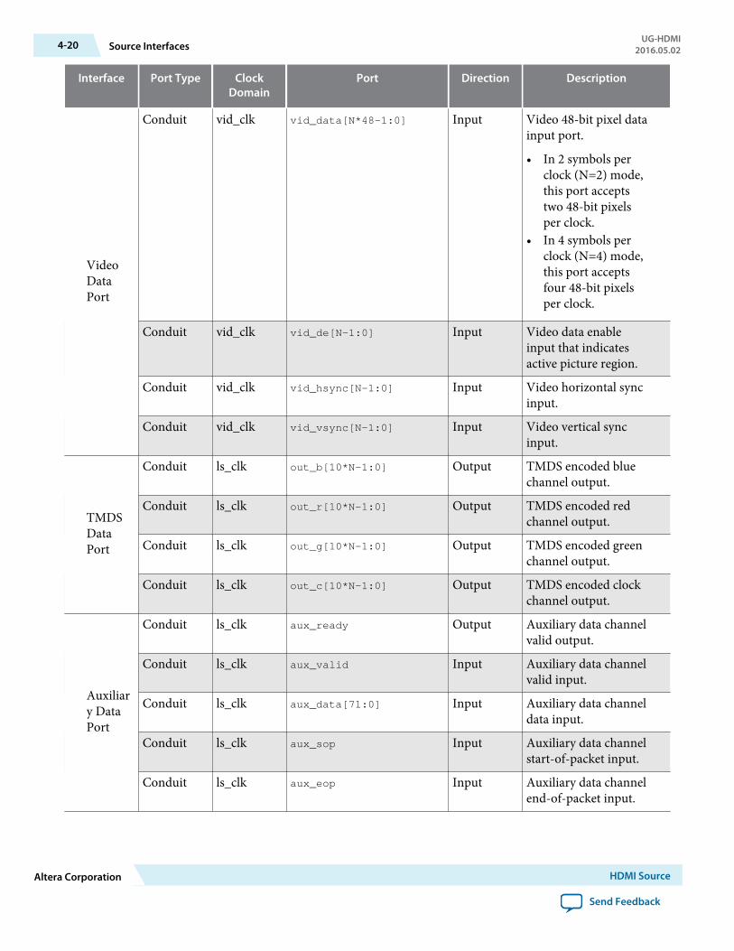
VideoDataPort
Conduit vid_clk vid_data[N*48-1:0] Input Video 48-bit pixel datainput port.
• In 2 symbols perclock (N=2) mode,this port acceptstwo 48-bit pixelsper clock.
• In 4 symbols perclock (N=4) mode,this port acceptsfour 48-bit pixelsper clock.
Conduit vid_clk vid_de[N-1:0] Input Video data enableinput that indicatesactive picture region.
Conduit vid_clk vid_hsync[N-1:0] Input Video horizontal syncinput.
Conduit vid_clk vid_vsync[N-1:0] Input Video vertical syncinput.
TMDSDataPort
Conduit ls_clk out_b[10*N-1:0] Output TMDS encoded bluechannel output.
Conduit ls_clk out_r[10*N-1:0] Output TMDS encoded redchannel output.
Conduit ls_clk out_g[10*N-1:0] Output TMDS encoded greenchannel output.
Conduit ls_clk out_c[10*N-1:0] Output TMDS encoded clockchannel output.
Auxiliary DataPort
Conduit ls_clk aux_ready Output Auxiliary data channelvalid output.
Conduit ls_clk aux_valid Input Auxiliary data channelvalid input.
Conduit ls_clk aux_data[71:0] Input Auxiliary data channeldata input.
Conduit ls_clk aux_sop Input Auxiliary data channelstart-of-packet input.
Conduit ls_clk aux_eop Input Auxiliary data channelend-of-packet input.
4-20 Source InterfacesUG-HDMI
2016.05.02
Altera Corporation HDMI Source
Send Feedback
Interface Port Type ClockDomain
Port Direction Description
EncoderControlPort
Conduit ls_clk mode Input Encoding mode input.
• 0 = DVI• 1 = HDMI
Conduit ls_clk TMDS_Bit_clock_Ratio Input • 0 = (TMDS bitperiod) / (TMDSclock period) ratiois 1/10
• 1 = (TMDS bitperiod) / (TMDSclock period) ratiois 1/40
Conduit ls_clk Scrambler_Enable Input • 0 = Instructs thesource device notto performscrambling
• 1 = Instructs thesource device toperformscrambling
Conduit ls_clk ctrl[6*N-1:0] Input DVI control side-bandinputs to override thenecessary control andsynchronization datain the green and redchannels.
AudioPort
Conduit audio_clk audio_CTS[19:0] Input Audio CTS valueinput.
Conduit audio_clk audio_N[19:0] Input Audio N value input.
Conduit audio_clk audio_data[255:0] Input Audio data input.
M is 1 when youenable support for 8-channel audio.Otherwise it is 0.
UG-HDMI2016.05.02 Source Interfaces 4-21
HDMI Source Altera Corporation
Send Feedback
Interface Port Type ClockDomain
Port Direction Description
Conduit audio_clk audio_de[7:0] Input Audio data validinput.
• audio_de[0] mustbe asserted totransmit the audiodata for all audiochannels.
• audio_de[2]
indicates whetherthe audio is sent in2-channel layout or8-channel layout.
When audio_de[2] is 0, audiodata is transmittedin 2-channellayout.
When audio_de[2] is 1, audiodata is transmittedin 8-channellayout.
• audio_de[1] andaudio_de[7:3] arereserved bits.
M is 1 when youenable support for 8-channel audio.Otherwise it is 0.
Conduit audio_clk audio_mute Input Audio mute input.
Conduit audio_clk audio_info_ai[48:0] Input Audio InfoFrameinput bundle input.
Conduit audio_clk audio_metadata[165:0] Input Carries additionalinformation related to3D audio andmultistream audio.
Conduit audio_clk audio_format[4:0] Input Indicates the audioformat to betransmitted.
4-22 Source InterfacesUG-HDMI
2016.05.02
Altera Corporation HDMI Source
Send Feedback
Interface Port Type ClockDomain
Port Direction Description
AuxiliaryControlPort
Conduit ls_clk gcp[5:0] Input General ControlPacket.
Conduit ls_clk info_avi[112:0] Input Auxiliary VideoInformationInfoFrame input.
Conduit ls_clk info_vsi[61:0] Input Vendor SpecificInformationInfoFrame input.
Source Clock TreeThe source uses various clocks.
UG-HDMI2016.05.02 Source Clock Tree 4-23
HDMI Source Altera Corporation
Send Feedback
Figure 4-19: Source Clock Tree
The figure shows how the different clocks connect in the source core.
ResamplerFIFO
Sync
TMDS(TERC4)Encoder
Sync
Sync
Sync
HSSI[0]
HSSI[1]
HSSI[2]
HSSI[3]
HDMI Source Core
Channel [0]
Channel [1]
Channel [2]
Channel [3]
WRCLK RDCLK
WRCLK RDCLK
WRCLK RDCLK
WRCLK RDCLK
WRCLK RDCLK
ls_clkvid_clk
Pixel Data
AUX Data
Transceiver
TransceiverPLLGPLL
CLK0CLK1CLK2
reconfig
ls_clkvid_clk
tx_clk[0]
The pixel data clocks into the core at the pixel clock (vid_clk). This same clock derives the required linkspeed clock (ls_clk), which is used to drive the transceiver phase-locked loop (PLL) input. The ls_clkdepends on the color bits per pixel (bpp).
Because the transceiver is in bonding mode, the HDMI source core uses tx_clk[0] to clock the data fromthe source core in the ls_clk domain into the transceiver in the tx_clk[0] domain.
For HDMI source, you must instantiate 4 transmitter channels: 3 channels to transmit data and 1 channelto transmit clock information.
You must connect the core ls_clk to the transceiver clock output, which performs the TMDS and TERC4encoding. The auxiliary data clocks into the core at the ls_clk rate.
4-24 Source Clock TreeUG-HDMI
2016.05.02
Altera Corporation HDMI Source
Send Feedback

Related InformationHDMI Hardware Demonstration on page 6-1For more information about the transmitter and receiver channels.
UG-HDMI2016.05.02 Source Clock Tree 4-25
HDMI Source Altera Corporation
Send Feedback
HDMI Sink 52016.05.02
UG-HDMI Subscribe Send Feedback
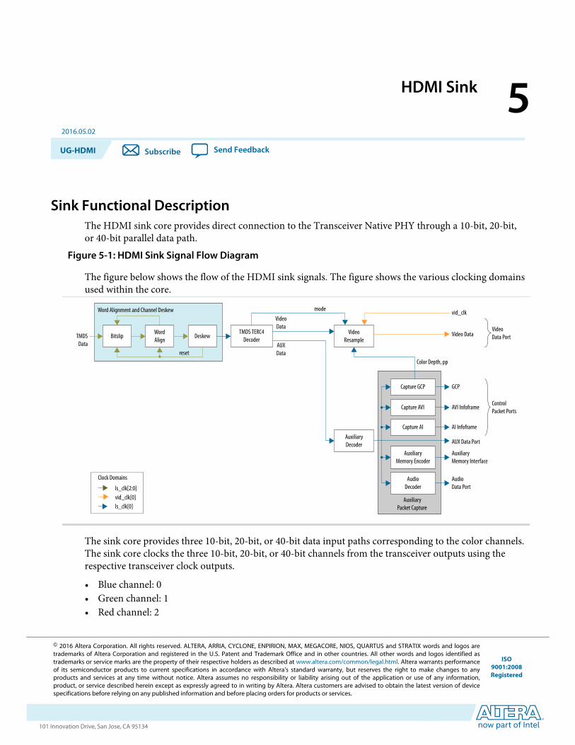
Sink Functional DescriptionThe HDMI sink core provides direct connection to the Transceiver Native PHY through a 10-bit, 20-bit,or 40-bit parallel data path.
Figure 5-1: HDMI Sink Signal Flow Diagram
The figure below shows the flow of the HDMI sink signals. The figure shows the various clocking domainsused within the core.
VideoResample
AuxiliaryDecoder
AudioDecoder
TMDS TERC4Decoder
AuxiliaryMemory Encoder
Capture AI
Capture AVI
Capture GCP
Color Depth, pp
GCP
AudioData Port
AuxiliaryMemory Interface
AI Infoframe
AVI Infoframe
AUX Data Port
AuxiliaryPacket Capture
ControlPacket Ports
VideoData Port
vid_clk
Video Data
mode
VideoData
AUXData
DeskewWordAlign
Bitslip
reset
Word Alignment and Channel Deskew
TMDSData
ls_clk[2:0]vid_clk[0]ls_clk[0]
Clock Domains
The sink core provides three 10-bit, 20-bit, or 40-bit data input paths corresponding to the color channels.The sink core clocks the three 10-bit, 20-bit, or 40-bit channels from the transceiver outputs using therespective transceiver clock outputs.
• Blue channel: 0• Green channel: 1• Red channel: 2
© 2016 Altera Corporation. All rights reserved. ALTERA, ARRIA, CYCLONE, ENPIRION, MAX, MEGACORE, NIOS, QUARTUS and STRATIX words and logos aretrademarks of Altera Corporation and registered in the U.S. Patent and Trademark Office and in other countries. All other words and logos identified astrademarks or service marks are the property of their respective holders as described at www.altera.com/common/legal.html. Altera warrants performanceof its semiconductor products to current specifications in accordance with Altera's standard warranty, but reserves the right to make changes to anyproducts and services at any time without notice. Altera assumes no responsibility or liability arising out of the application or use of any information,product, or service described herein except as expressly agreed to in writing by Altera. Altera customers are advised to obtain the latest version of devicespecifications before relying on any published information and before placing orders for products or services.
ISO9001:2008Registered
www.altera.com101 Innovation Drive, San Jose, CA 95134
Sink Channel Word Alignment and DeskewThe input stage of the sink is responsible for synchronizing the incoming parallel data channels correctly.The synchronization is split to two stages: word alignment and channel deskew.
Table 5-1: Synchronization Stages
Stage Description
Word Alignment • Correctly aligns the incoming parallel data to word boundaries using bit-sliptechnique.
• TMDS encoding does not guarantee unique control codes, but the core canstill use the sequence of continuous symbols found in data and videopreambles to align.
• The alignment algorithm searches for 12 consecutive 0×54 or 0×abcorresponding to the data and video preambles.
Note: The preambles are also present in digital video interface (DVI)coding.
• The alignment logic asserts a marker indicator when the 12 consecutivesignals are detected.
• Similarly, the logic infers alignment loss when 8K symbol clocks elapsewithout a single marker assertion.
Channel Deskew • When the data channels are aligned, the core then attempts to deskew eachchannel.
• The sink core deskews at the rising edge of the marker insertion.• For every correct deskewed lane, the marker insertion will appear in all three
TMDS encoded streams.• The sink core deskews using three dual-clock FIFOs.• The dual-clock FIFOs also synchronize all three data streams to the blue
channel clock to be used later throughout the decoder core.
5-2 Sink Channel Word Alignment and DeskewUG-HDMI
2016.05.02
Altera Corporation HDMI Sink
Send Feedback
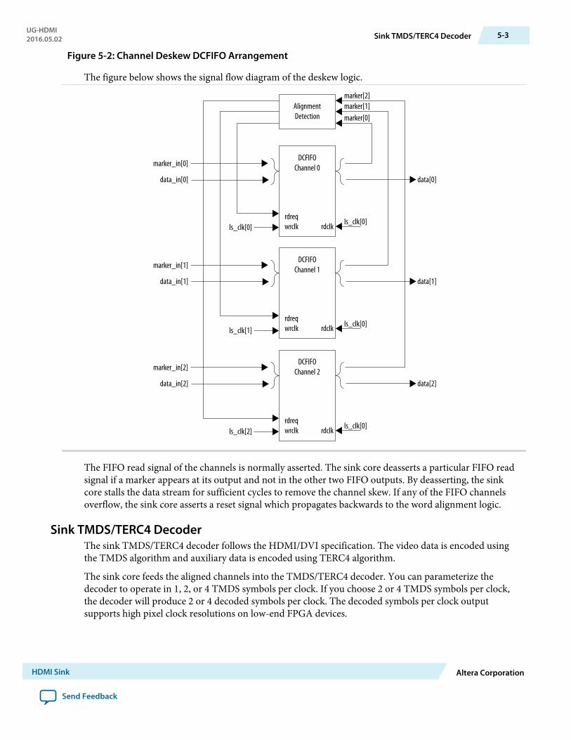
Figure 5-2: Channel Deskew DCFIFO Arrangement
The figure below shows the signal flow diagram of the deskew logic.
AlignmentDetection
DCFIFOChannel 0
rdreqwrclk rdclk
DCFIFOChannel 1
rdreqwrclk rdclk
DCFIFOChannel 2
rdreqwrclk rdclk
ls_clk[0]
ls_clk[0]
ls_clk[0]ls_clk[2]
ls_clk[1]
ls_clk[0]
marker_in[0]
data_in[0] data[0]
marker_in[1]
data_in[1] data[1]
marker_in[2]
data_in[2] data[2]
marker[2]marker[1]marker[0]
The FIFO read signal of the channels is normally asserted. The sink core deasserts a particular FIFO readsignal if a marker appears at its output and not in the other two FIFO outputs. By deasserting, the sinkcore stalls the data stream for sufficient cycles to remove the channel skew. If any of the FIFO channelsoverflow, the sink core asserts a reset signal which propagates backwards to the word alignment logic.
Sink TMDS/TERC4 DecoderThe sink TMDS/TERC4 decoder follows the HDMI/DVI specification. The video data is encoded usingthe TMDS algorithm and auxiliary data is encoded using TERC4 algorithm.
The sink core feeds the aligned channels into the TMDS/TERC4 decoder. You can parameterize thedecoder to operate in 1, 2, or 4 TMDS symbols per clock. If you choose 2 or 4 TMDS symbols per clock,the decoder will produce 2 or 4 decoded symbols per clock. The decoded symbols per clock outputsupports high pixel clock resolutions on low-end FPGA devices.
UG-HDMI2016.05.02 Sink TMDS/TERC4 Decoder 5-3
HDMI Sink Altera Corporation
Send Feedback

Sink Video ResamplerThe video resampler consists of a gearbox and a dual-clock FIFO (DCFIFO).
The gearbox converts 8-bpc data to 8-, 10-, 12- or 16-bpc data based on the current color depth. The GCPconveys the color depth information.
Figure 5-3: Sink Resampler Signal Flow Diagram
H-SYNCV-SYNCde
1
vid_clk
DCFIFO
ls_clk
q
rd
rdwrclk
data
wr
wrclk
PhaseCounter
Gearbox
H-SYNCV-SYNC
de
Resampled
pp
bpp
b[15:0]
r[15:0]g[15:0]
b[7:0]
r[7:0]g[7:0]
The resampler adheres to the recommended phase count method described in HDMI Specification Ver.1.4b.
• To keep the source and sink resamples synchronized, the source must send the phase-packing (pp)value to the sink during the vertical blanking phase, using the general control packet.
• The pp corresponds to the phase of the last pixel in the last active video line.• The phase-counter logic compares its own pp value to the pp value received in the general control
packet and slips the phase count if the two pp values do not agree.
The output from the resampler is fixed at 16 bpc. When the resampler operates in lower color depths, thelow order bits are zero.
Sink Auxiliary Decoder
The sink core decodes the auxiliary data path into a 72-bit wide standard packet stream. The streamcontains a valid, start-of-packet (SOP) and end-of-packet (EOP) marker.
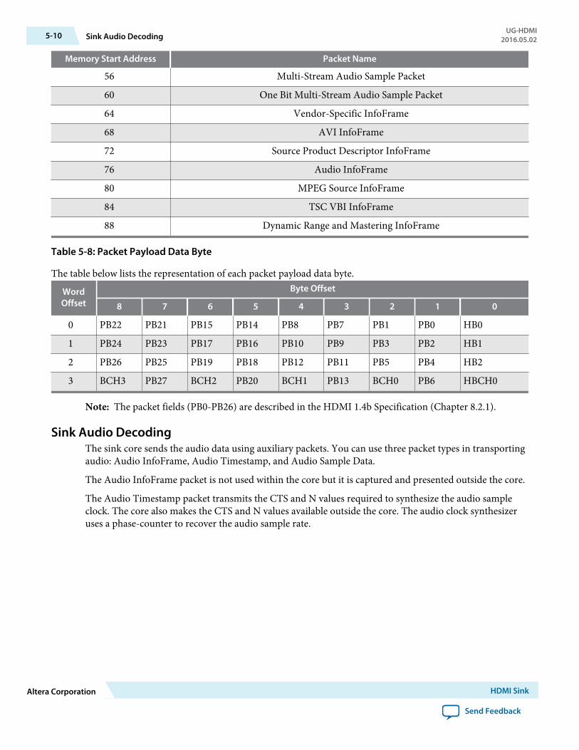
Table 5-2: Auxiliary Packet Memory Map
This table lists the addresses corresponding to the captured packets.Memory Start Address Packet Name
0 NULL PACKET
4 Audio Clock Regeneration (N/CTS)
8 Audio Sample
12 General Control
16 ACP Packet
20 ISRC1 Packet
5-4 Sink Video ResamplerUG-HDMI
2016.05.02
Altera Corporation HDMI Sink
Send Feedback
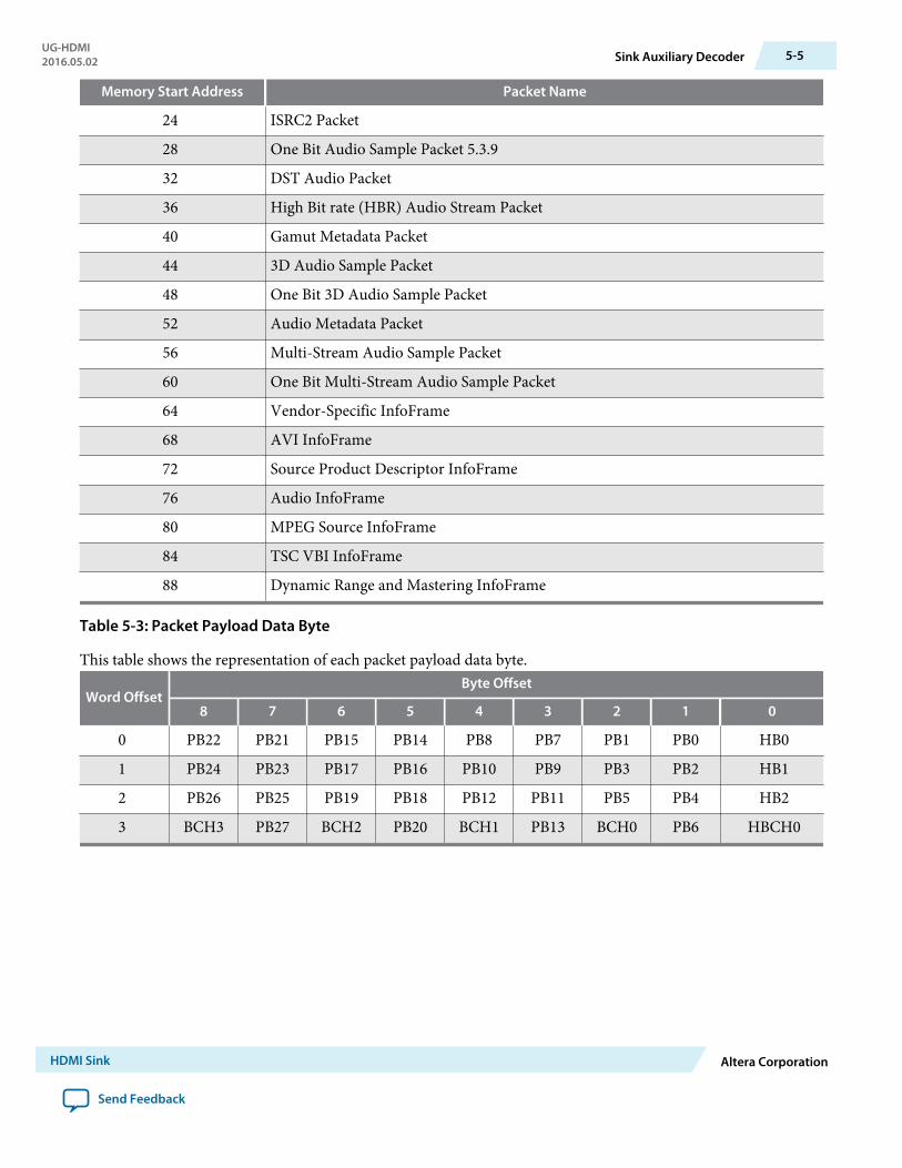
Memory Start Address Packet Name
24 ISRC2 Packet
28 One Bit Audio Sample Packet 5.3.9
32 DST Audio Packet
36 High Bit rate (HBR) Audio Stream Packet
40 Gamut Metadata Packet
44 3D Audio Sample Packet
48 One Bit 3D Audio Sample Packet
52 Audio Metadata Packet
56 Multi-Stream Audio Sample Packet
60 One Bit Multi-Stream Audio Sample Packet
64 Vendor-Specific InfoFrame
68 AVI InfoFrame
72 Source Product Descriptor InfoFrame
76 Audio InfoFrame
80 MPEG Source InfoFrame
84 TSC VBI InfoFrame
88 Dynamic Range and Mastering InfoFrame
Table 5-3: Packet Payload Data Byte
This table shows the representation of each packet payload data byte.
Word OffsetByte Offset
8 7 6 5 4 3 2 1 0
0 PB22 PB21 PB15 PB14 PB8 PB7 PB1 PB0 HB0
1 PB24 PB23 PB17 PB16 PB10 PB9 PB3 PB2 HB1
2 PB26 PB25 PB19 PB18 PB12 PB11 PB5 PB4 HB2
3 BCH3 PB27 BCH2 PB20 BCH1 PB13 BCH0 PB6 HBCH0
UG-HDMI2016.05.02 Sink Auxiliary Decoder 5-5
HDMI Sink Altera Corporation
Send Feedback

Figure 5-4: Auxiliary Data Stream Signal
The figure below shows the relationship between the data bit-field and its clock cycle based on 1-, 2-, or 4-symbol per clock mode.
PB22
PB21
PB15
PB14
PB8
PB7
PB1
PB0
HB0
Phase 0
PB24
PB23
PB17
PB16
PB10
PB9
PB3
PB2
HB1
Phase 1
PB26
PB25
PB19
PB18
PB12
PB11
PB5
PB4
HB2
Phase 2
BCH3
PB27
BCH2
PB20
BCH1
PB13
BCH0
PB6
0
Phase 3
BCH Block 3
BCH Block 2
BCH Block 1
BCH Block 0
Output Data
Byte[8]
Byte[0]
Startofpacket
Endofpacket
Valid
Clock
0 - - 8 - - 16 - - 24Cycle 1 Symbol
0 - - 4 - - 8 - - 12Cycle 2 Symbol
0 - - 2 - - 4 - - 6Cycle 4 Symbol
Phase 0 Phase 1 Phase 2 Phase 3
The data output at EOP contains the received BCH error correcting code. The sink core does not performany error correction within the core. The auxiliary data is available outside the core.
Note: You can find the bit-field nomenclature in the HDMI Specification Ver.2.0.
Sink Auxiliary Packet CaptureThe auxiliary streams transfer auxiliary packets.
The auxiliary packets can carry 15 different packet types.
The module produces 4 valid signals to simplify the user logic.
To simplify user applications and minimize external logic, the HDMI core captures 3 different packettypes and decodes the audio sample data. These packets are: General Control Packet, Auxiliary VideoInformation (AVI) InfoFrame, and HDMI Vendor Specific InfoFrame (VSI).
Sink General Control Packet
5-6 Sink Auxiliary Packet CaptureUG-HDMI
2016.05.02
Altera Corporation HDMI Sink
Send Feedback

Table 5-4: General Control Packet Input Fields
Bit Field Name Comment
gcp[3:0] Color Depth(CD)
CD3 CD2 CD1 CD0 Color depth
0 0 0 0 Color depth notindicated
0 0 0 1 Reserved
0 0 1 0 Reserved
0 0 1 1 Reserved
0 1 0 0 8 bpc or 24 bpp
0 1 0 1 10 bpc or 30bpp
0 1 1 0 12 bpc or 36bpp
0 1 1 1 16 bpc or 48bpp
1 1 1 1 Reserved
gcp[4] Set_AVMUTE
Refer to HDMI Specification Ver.1.4b
gcp[5] Clear_AVMUTE
Refer to HDMI Specification Ver.1.4b
Sink Auxiliary Video Information (AVI) InfoFrameThe HDMI core produces AVI InfoFrame to simplify user applications.
Table 5-5: Auxiliary Video Information (AVI) InfoFrame Bit-Fields
The table below lists the bit-fields for the AVI InfoFrame port bundle.
The signal bundle is clocked by ls_clk.
Bit-field Default Value(Hexadecimal)
Name Comment
7:0 67 Checksum Checksum
9:8 0 S Scan information
11:10 0 B Bar info data valid
12 0 A0 Active information present
14:13 0 Y RGB or YCbCr indicator
15 0 Reserved Returns 0
19:16 8 R Active format aspect ratio
UG-HDMI2016.05.02 Sink Auxiliary Video Information (AVI) InfoFrame 5-7
HDMI Sink Altera Corporation
Send Feedback

Bit-field Default Value(Hexadecimal)
Name Comment
21:20 0 M Picture aspect ratio
23:22 0 C Colorimetry (for example: ITU BT.601,BT.709)
25:24 0 SC Non-uniform picture scaling
27:26 0 Q Quantization range
30:28 0 EC Extended colorimetry
31 0 ITC IT content
38:32 00 VIC Video format identification code
39 0 Reserved Returns 0
43:40 0 PR Picture repetition factor
45:44 0 CN Content type
47:46 0 YQ YCC quantization range
63:48 0000 ETB Line number of end of top bar
79:64 0000 SBB Line number of start of bottom bar
95:80 0000 ELB Pixel number of end of left bar
111:96 0000 SRB Pixel number of start of right bar
Sink HDMI Vendor Specific InfoFrame (VSI)The core produces the captured HDMI Vendor Specific InfoFrame to simplify user applications.
Table 5-6: HDMI Vendor Specific InfoFrame Bit-Fields
The table below lists the bit-fields for VSI.
The signal bundle is clocked by ls_clk.
Bit-field Default Value(Hexadecimal)
Name Comment
4:0 06 Length Length = Nv
12:5 69 Checksum Checksum
36:13 000C03 IEEE 24-bit IEEE registration identified(0x000C03)
41:37 00 Reserved All 0
44:42 0 HDMI_Video_Format
HDMI video format
52:45 00 HDMI_VIC HDMI proprietary video formatidentification code
5-8 Sink HDMI Vendor Specific InfoFrame (VSI)UG-HDMI
2016.05.02
Altera Corporation HDMI Sink
Send Feedback

Bit-field Default Value(Hexadecimal)
Name Comment
57:53 00 Reserved All 0
60:58 0 3D_Ext_Data 3D extended data
Sink Auxiliary Data PortThe auxiliary port is attached to external memory. This port allows you to write packets to memory foruse outside the HDMI core.
The core calculates the address for the data port using the header byte of the received packet. The corewrites packet types 0–15 into a contiguous memory region.
Figure 5-5: Typical Application of AUX Packet Register Interface
The figure below shows a typical application of the auxiliary data port.
data[71:0]HDMI Sink Core
wraddr[6:0] On-Chip
Memory
data[71:8]
rdaddr[6:0]
From 64 bitNios IIAvalon-MM
Table 5-7: Auxiliary Packet Memory Map
Memory Start Address Packet Name
0 NULL PACKET
4 Audio Clock Regeneration (N/CTS)
8 Audio Sample
12 General Control
16 ACP Packet
20 ISRC1 Packet
24 ISRC2 Packet
28 One Bit Audio Sample Packet 5.3.9
32 DST Audio Packet
36 High Bitrate (HBR) Audio Stream Packet
40 Gamut Metadata Packet
44 3D Audio Sample Packet
48 One Bit 3D Audio Sample Packet
52 Audio Metadata Packet
UG-HDMI2016.05.02 Sink Auxiliary Data Port 5-9
HDMI Sink Altera Corporation
Send Feedback
Memory Start Address Packet Name
56 Multi-Stream Audio Sample Packet
60 One Bit Multi-Stream Audio Sample Packet
64 Vendor-Specific InfoFrame
68 AVI InfoFrame
72 Source Product Descriptor InfoFrame
76 Audio InfoFrame
80 MPEG Source InfoFrame
84 TSC VBI InfoFrame
88 Dynamic Range and Mastering InfoFrame
Table 5-8: Packet Payload Data Byte
The table below lists the representation of each packet payload data byte.
WordOffset
Byte Offset
8 7 6 5 4 3 2 1 0
0 PB22 PB21 PB15 PB14 PB8 PB7 PB1 PB0 HB0
1 PB24 PB23 PB17 PB16 PB10 PB9 PB3 PB2 HB1
2 PB26 PB25 PB19 PB18 PB12 PB11 PB5 PB4 HB2
3 BCH3 PB27 BCH2 PB20 BCH1 PB13 BCH0 PB6 HBCH0
Note: The packet fields (PB0-PB26) are described in the HDMI 1.4b Specification (Chapter 8.2.1).
Sink Audio DecodingThe sink core sends the audio data using auxiliary packets. You can use three packet types in transportingaudio: Audio InfoFrame, Audio Timestamp, and Audio Sample Data.
The Audio InfoFrame packet is not used within the core but it is captured and presented outside the core.
The Audio Timestamp packet transmits the CTS and N values required to synthesize the audio sampleclock. The core also makes the CTS and N values available outside the core. The audio clock synthesizeruses a phase-counter to recover the audio sample rate.
5-10 Sink Audio DecodingUG-HDMI
2016.05.02
Altera Corporation HDMI Sink
Send Feedback

Figure 5-6: Audio Decoder Signal Flow
Capture AudioTimestamp
AudioDepacketizer
Valid
AudioSample
Capture AudioInfoFrame
Capture AudioInfoFrame
wr
AuxiliaryStreamPackets
Audio Data
data
rd
q
CTS, N
Capture AudioInfoFrame
AI InfoFrame
Capture AudioInfoFrame
Audio Metadata
Audio Valid
Audio LPCM
Audio Format
The output from the audio clock synthesizer generates a valid pulse at the same rate as the audio sampleclock used in the HDMI source device. This valid pulse is available outside the core as an audio samplevalid signal. This signal reads from a FIFO, which governs the rate of audio samples. The audio depacke‐tizer drives the input to the FIFO.
The audio depacketizer extracts the 32-bit audio sample data from the incoming Audio Sample packets.The Audio Sample packets can hold from one to four sample data values. The audio format indicates theformat of the received audio data.
Table 5-9: Definition of HDMI Sink Audio Format
Value Name Description
0 LPCM HDMI packet type 2 transports payload data
1 One-Bit Audio HDMI packet type 7 transports payload data (notsupported)
2 DST Audio HDMI packet type 8 transports payload data (notsupported)
3 HBR HDMI packet type 9 transports payload data
4 3D (LPCM) HDMI packet type 11 transports payload data (notsupported)
5 3D (One-Bit) HDMI packet type 12 transports payload data (notsupported)
6 MST (LPCM) HDMI packet type 14 transports payload data
7 MST (One-Bit) HDMI packet type 15 transports payload data (notsupported)
8–15 — Reserved
UG-HDMI2016.05.02 Sink Audio Decoding 5-11
HDMI Sink Altera Corporation
Send Feedback
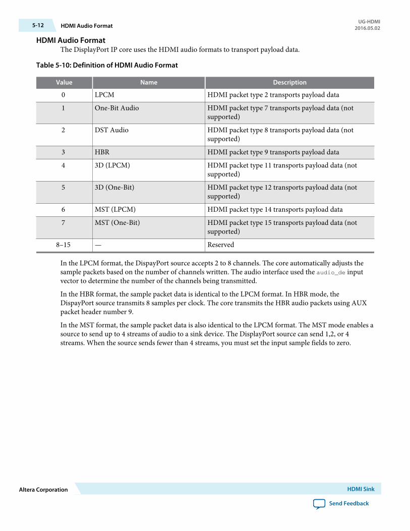
HDMI Audio FormatThe DisplayPort IP core uses the HDMI audio formats to transport payload data.
Table 5-10: Definition of HDMI Audio Format
Value Name Description
0 LPCM HDMI packet type 2 transports payload data
1 One-Bit Audio HDMI packet type 7 transports payload data (notsupported)
2 DST Audio HDMI packet type 8 transports payload data (notsupported)
3 HBR HDMI packet type 9 transports payload data
4 3D (LPCM) HDMI packet type 11 transports payload data (notsupported)
5 3D (One-Bit) HDMI packet type 12 transports payload data (notsupported)
6 MST (LPCM) HDMI packet type 14 transports payload data
7 MST (One-Bit) HDMI packet type 15 transports payload data (notsupported)
8–15 — Reserved
In the LPCM format, the DispayPort source accepts 2 to 8 channels. The core automatically adjusts thesample packets based on the number of channels written. The audio interface used the audio_de inputvector to determine the number of the channels being transmitted.
In the HBR format, the sample packet data is identical to the LPCM format. In HBR mode, theDispayPort source transmits 8 samples per clock. The core transmits the HBR audio packets using AUXpacket header number 9.
In the MST format, the sample packet data is also identical to the LPCM format. The MST mode enables asource to send up to 4 streams of audio to a sink device. The DisplayPort source can send 1,2, or 4streams. When the source sends fewer than 4 streams, you must set the input sample fields to zero.
5-12 HDMI Audio FormatUG-HDMI
2016.05.02
Altera Corporation HDMI Sink
Send Feedback

Figure 5-7: MST Audio Format
ST3-L
ST3-R
ST2-L
ST2-R
ST1-L
ST1-R
ST0-L
ST0-R
4 Streams
0
0
0
0
ST1-L
ST1-R
ST0-L
ST0-R
2 Streams
0
0
0
0
0
0
ST0-L
ST0-R
1 Stream
Audio InfoFrameThe sink produces the received Audio InfoFrame (AI) to simplify user applications.
Table 5-11: Audio InfoFrame Bundle Bit Fields
This table defines the signal bit fields. ls_clk clocks the signal bundle.Bit Field Name Description
7:0 Checksum Checksum
10:8 CC Channel count
11 Reserved Returns zero
15:12 CT Audio format type
17:16 SS Bits-per-audio sample
20:18 SF Sampling frequency
23:21 Reserved Returns zero
31:24 CXT Audio format type of the audio stream
39:32 CA Speaker location allocation: front left (FL), frontright (FR)
41:40 LFEPBL Low-frequency effects (LFE) playback levelinformation, Decibel (dB)
42 Reserved Returns zero
46:43 LSV Level shift information, dB
47 DM_INH Down-mix inhibit flag
UG-HDMI2016.05.02 Audio InfoFrame 5-13
HDMI Sink Altera Corporation
Send Feedback

Audio MetadataThe HDMI 2.0 specification introduces the Audio Metadata (AM) Packet. The Audio Metadata packetmanages the Multi-Stream and 3D audio sample packets.
Table 5-12: Audio Metadata Bundle Bit Fields
This table defines the signal bit fields.Bit Field Name Description
0 3D_AUDIO • 1 = Transmits 3D audio• 0 = Transmits MST
2:1 NUM_VIEWS Indicates the number of views for an MST stream
4:3 NUM_AUDIO_STR Number of audio streams
164:5 Payload data Corresponds to PB0 to PB19 of the Metadatapackets.
165 ACTIVE When asserted, the core never sends the Metadata.
Note: For more information, refer to the HDMI 2.0 Specification, Chapter 8.3 Audio Metadata Packet.
Sink ParametersYou set parameters for the sink using the Altera HDMI parameter editor.
Table 5-13: HDMI Sink Parameters
Parameter Value Description
Device family Stratix V
Arria V
Arria 10
Targeted device family; matches the projectdevice family.
Direction Transmitter = Source
Receiver = Sink
Select HDMI sink.
Symbols per clock 1, 2, or 4 symbols perclock
Determines how many TMDS symbols and pixelsare processed per clock.
• Stratix V supports 1 or 2 symbols per clock• Arria V supports 1, 2, or 4 symbols per clock• Arria 10 supports only 2 symbols per clock
Support auxiliary 0 = No AUX
1 = AUX
Determines if auxiliary channel encoding isincluded.
5-14 Audio MetadataUG-HDMI
2016.05.02
Altera Corporation HDMI Sink
Send Feedback

Parameter Value Description
Support deep color 0 = No deep color
1 = Deep color
Determines if the core can encode deep colorformats.
To enable this parameter, you must also enablethe Support auxiliary parameter.
Support audio 0 = No audio
1 = Audio
Determines if the core can encode audio data.
To enable this parameter, you must also enablethe Support auxiliary parameter.
Support 8-channel audio 0 = No
1 = Yes
Determines if the core can support up to 8 audiochannels. Enable this parameter if you want tosupport more than the default 2 audio channels.
To enable this parameter, you must also enablethe Support audio parameter.
Manufacturer OUI — The Manufacturer Organizationally UniqueIdentifier (OUI) assigned to the manufactureddevice to be written into the SCDC registers ofaddress 0xD0, 0xD1, and 0xD2.
Key in 3 byte hexadecimal data.
Device ID String — The Device Identification (ID) string to bewritten into the SCDC registers from addressses0xD3 to 0xDa.
Use this parameter to identify the sink device.You can key in up to eight ASCII characters. Ifyou use less than eight characters, the unusedbytes are be set to 0x00.
Hardware Revision — Indicates the major and minor revisions of thehardware. Key in one byte of integer data.
• Upper byte represents major revision.• Lower byte represents minor revision.
The hardware major revision increments on amajor silicon or board revision. The hardwareminor revision increments on a minor siliconrevision or minor board revision and resets to 0when the major revision increments.
Sink InterfacesThe table lists the sink's port interfaces.
UG-HDMI2016.05.02 Sink Interfaces 5-15
HDMI Sink Altera Corporation
Send Feedback
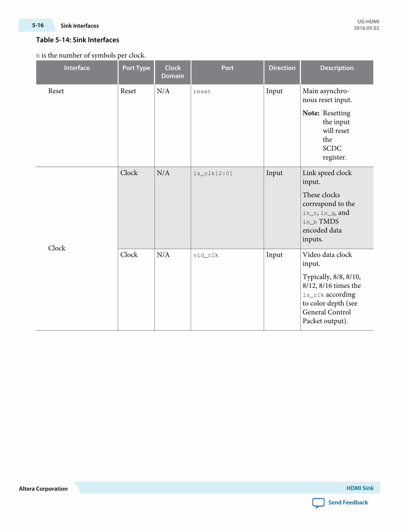
Table 5-14: Sink Interfaces
N is the number of symbols per clock.
Interface Port Type ClockDomain
Port Direction Description
Reset Reset N/A reset Input Main asynchro‐nous reset input.
Note: Resettingthe inputwill resettheSCDCregister.
Clock
Clock N/A ls_clk[2:0] Input Link speed clockinput.
These clockscorrespond to thein_r, in_g, andin_b TMDSencoded datainputs.
Clock N/A vid_clk Input Video data clockinput.
Typically, 8/8, 8/10,8/12, 8/16 times thels_clk accordingto color depth (seeGeneral ControlPacket output).
5-16 Sink InterfacesUG-HDMI
2016.05.02
Altera Corporation HDMI Sink
Send Feedback

Interface Port Type ClockDomain
Port Direction Description
Video Data Port
Conduit vid_clk vid_data[N*48-1:0] Output Video 48-bit pixeldata output port.
In 2 symbols perclock (N=2) mode,this port producestwo 48-bit pixelsper clock.
In 4 symbols perclock (N=4) mode,this port producesfour 48-bit pixelsper clock.
Conduit vid_clk vid_de[N-1:0] Output Video data enableoutput thatindicates activepicture region.
Conduit vid_clk vid_hsync[N-1:0] Output Video horizontalsync output.
Conduit vid_clk vid_vsync[N-1:0] Output Video vertical syncoutput.
Conduit vid_clk locked[2:0] Output Indicates that theHDMI sink core islocked to theTMDS signals.
Each bit representsa color channel.
Conduit vid_clk vid_lock Output Asserted when thereceived video datais determined to bestable andrepetitive.
UG-HDMI2016.05.02 Sink Interfaces 5-17
HDMI Sink Altera Corporation
Send Feedback
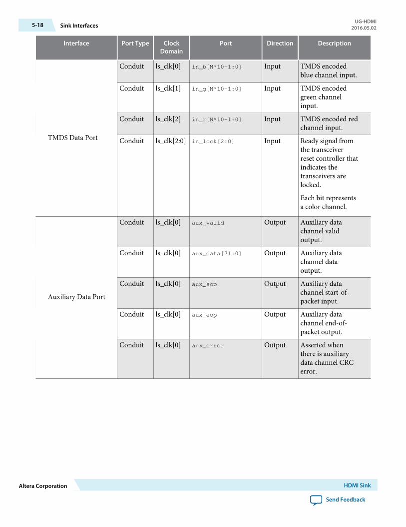
Interface Port Type ClockDomain
Port Direction Description
TMDS Data Port
Conduit ls_clk[0] in_b[N*10-1:0] Input TMDS encodedblue channel input.
Conduit ls_clk[1] in_g[N*10-1:0] Input TMDS encodedgreen channelinput.
Conduit ls_clk[2] in_r[N*10-1:0] Input TMDS encoded redchannel input.
Conduit ls_clk[2:0] in_lock[2:0] Input Ready signal fromthe transceiverreset controller thatindicates thetransceivers arelocked.
Each bit representsa color channel.
Auxiliary Data Port
Conduit ls_clk[0] aux_valid Output Auxiliary datachannel validoutput.
Conduit ls_clk[0] aux_data[71:0] Output Auxiliary datachannel dataoutput.
Conduit ls_clk[0] aux_sop Output Auxiliary datachannel start-of-packet input.
Conduit ls_clk[0] aux_eop Output Auxiliary datachannel end-of-packet output.
Conduit ls_clk[0] aux_error Output Asserted whenthere is auxiliarydata channel CRCerror.
5-18 Sink InterfacesUG-HDMI
2016.05.02
Altera Corporation HDMI Sink
Send Feedback

Interface Port Type ClockDomain
Port Direction Description
Decoder Control Port
Conduit ls_clk[0] TMDS_Bit_clock_
Ratio
Output • 0 = (TMDS bitperiod) /(TMDS clockperiod) ratio is1/10
• 1 = (TMDS bitperiod) /(TMDS clockperiod) ratio is1/40
Conduit ls_clk[0] ctrl[N*6-1:0] Output DVI Control side-band signals thatshow the data thatoverwrite thecontrol andsynchronizationcharacter in thegreen and redchannels.
Conduit ls_clk[0] mode Output Encoding mode
• 0 = DVI• 1 = HDMI
Audio Port
Conduit ls_clk[0] audio_CTS[19:0] Output Audio CTS valueoutput.
Conduit ls_clk[0] audio_N[19:0] Output Audio N valueoutput.
Conduit ls_clk[0] audio_data[255:0] Output Audio data output.
M is 1 when youenable support for8-channel audio.Otherwise it is 0.
Conduit ls_clk[0] audio_de[7:0] Output Audio data validoutput.
UG-HDMI2016.05.02 Sink Interfaces 5-19
HDMI Sink Altera Corporation
Send Feedback
Interface Port Type ClockDomain
Port Direction Description
• audio_de[0]
and audio_de[1]
correspond toSample PresentBit of Subpacket0 (audio_data[31:0] andaudio_
data[63:32])
• audio_de[2]
and audio_de[3]
correspond toSample PresentBit of Subpacket1 (audio_data[95:64]
and audio_data[127:96])
• audio_de[4]
and audio_de[5]
correspond toSample PresentBit of Subpacket2 (audio_data[159:128]
and audio_data[191:160]
)
• audio_de[6]
and audio_de[7]
corresponds toSample PresentBit of Subpacket3 (audio_data[223:192]
and audio_data[255:224]
)
5-20 Sink InterfacesUG-HDMI
2016.05.02
Altera Corporation HDMI Sink
Send Feedback
Interface Port Type ClockDomain
Port Direction Description
M is 1 when youenable support for8-channel audio.Otherwise it is 0.
Conduit audio_clk audio_
metadata[164:0]
Output Additionalinformation relatedto 3D audio andmultistream audio.
Conduit audio_clk audio_format[4:0] Output Indicates the audioformat detected.
Conduit ls_clk[0] audio_info_
ai[47:0]
Input Audio InfoFrameinput bundle.
Auxiliary MemoryInterface
Conduit ls_clk[0] aux_pkt_addr[6:0] Output Auxiliary packetmemory bufferaddress output.
Conduit ls_clk[0] aux_pkt_data[71:0] Output Auxiliary packetmemory bufferdata output.
Conduit ls_clk[0] aux_pkt_wr Output Auxiliary packetmemory bufferwrite strobe output.
Auxiliary Control Port
Conduit ls_clk[0] gcp[5:0] Output General ControlPacket output.
Conduit ls_clk[0] info_avi[111:0] Output Auxiliary VideoInformationInfoFrame output.
Conduit ls_clk[0] info_vsi[60:0] Output Vendor SpecificInformationInfoFrame output.
SCDC Control Port
Conduit scdc_i2c_clk
in_5v_power Input Detects thepresence of 5Vinput voltage.
Conduit scdc_i2c_clk
in_hpd Input Detects the HotPlug Detect (HPD)status.
UG-HDMI2016.05.02 Sink Interfaces 5-21
HDMI Sink Altera Corporation
Send Feedback
Avalon-MM SCDC Management Interface
Table 5-15: Avalon-MM Status and Control Data Channel (SCDC) Management Interface Signals
The table lists the Avalon Memory-Mapped (Avalon-MM) Status and Control Data Channel (SCDC)Management interface signals.
Signal Direction Description
scdc_i2c_clk Input Avalon-MM clock input.
scdc_i2c_addr[7:0] Input 8-bit Avalon-MM address.
scdc_i2c_r Input Read signal.
scdc_i2c_rdata[7:0] Output Output data.
scdc_i2c_w Input Write signal.
scdc_i2c_wdata[7:0] Input Input data.
For more information about SCDC, refer to the HDMI 2.0 Specification Section 10.4 (Status and ControlData Channel).
Status and Control Data Channel InterfaceFor applications using the HDMI 2.0 feature, the HDMI IP core provides a memory slave port to theSCDC registers.
This memory slave port connects to an I2C slave component. The TMDS_Bit_clock_Ratio output fromthe SCDC interface indicates when the core requires the 1/40 TMDS bit period to TMDS clock period.This bit is also stored in its corresponding field in the SCDC registers.
The HDMI 2.0 specification requires the core to respond to the presence of the 5V input from theconnector and also the state of the HPD signal. The 5V input and HPD signal are used in the registermechanism updates. The signals are synchronous to the scdc_i2c_clk clock domain. You must create a100-ms delay on the HPD signal externally to the core.
For more information about the Status and Control Data Channel, you may refer to HDMI 2.0 Specifica‐tion Chapter 10.4.You can obtain the address map for the registers in the HDMI 2.0 specification.
Sink Clock TreeThe sink core uses different clocks.
The logic clocks the transceiver data into the core using the three CDR clocks: (rx_clk[2:0]).
The TMDS and TERC4 decoding is done at the link-speed clock (ls_clk). The sink then resamples thepixel data and presents the data at the output of the core at the video pixel clock (vid_clk).
The pixel data clock depends on the video format used (within HDMI specification).
For HDMI sink, you need to instantiate 3 receiver channels to receive data.
5-22 Avalon-MM SCDC Management InterfaceUG-HDMI
2016.05.02
Altera Corporation HDMI Sink
Send Feedback
Figure 5-8: Sink Clock Tree
The figure shows how the different clocks can be selected for the sink core.
ResamplerFIFO
Sync
TMDS(TERC4)Decoder
Sync
Sync
HSSI[0]
HSSI[1]
HSSI[2]
HDMI Sink Core
Channel [0]
reconfig
Channel [1]
Channel [2]
WRCLK RDCLK
WRCLK RDCLK
WRCLK RDCLK
WRCLK RDCLK
rx_clk[0] vid_clk
Pixel Data
AUX Data
Transceiver
GPLLCLK0CLK1CLK2
ls_clkvid_clk
ls_clk
TMDS Clock
CDR Reference Clock
rx_clk[1]
rx_clk[2]
Related InformationHDMI Hardware Demonstration on page 6-1For more information about the transmitter and receiver channels.
UG-HDMI2016.05.02 Sink Clock Tree 5-23
HDMI Sink Altera Corporation
Send Feedback
HDMI Hardware Demonstration 62016.05.02
UG-HDMI Subscribe Send Feedback
The Altera High-Definition Multimedia Interface (HDMI) hardware demonstration helps you evaluatethe functionality of the HDMI IP core and provides a starting point for you to create your own design.
The demonstration runs on the following device kits:
• Arria 10 development kit• Arria V GX starter kit• Stratix V GX development kit
Related InformationDesign Guidelines for DisplayPort and HDMI Interfaces
Hardware Demonstration ComponentsThe demonstration designs instantiate the Video and Image Processing (VIP) Suite IP cores or FIFObuffers to perform a direct HDMI video stream passthrough between the HDMI sink and source.
© 2016 Altera Corporation. All rights reserved. ALTERA, ARRIA, CYCLONE, ENPIRION, MAX, MEGACORE, NIOS, QUARTUS and STRATIX words and logos aretrademarks of Altera Corporation and registered in the U.S. Patent and Trademark Office and in other countries. All other words and logos identified astrademarks or service marks are the property of their respective holders as described at www.altera.com/common/legal.html. Altera warrants performanceof its semiconductor products to current specifications in accordance with Altera's standard warranty, but reserves the right to make changes to anyproducts and services at any time without notice. Altera assumes no responsibility or liability arising out of the application or use of any information,product, or service described herein except as expressly agreed to in writing by Altera. Altera customers are advised to obtain the latest version of devicespecifications before relying on any published information and before placing orders for products or services.
ISO9001:2008Registered
www.altera.com101 Innovation Drive, San Jose, CA 95134

The hardware demonstration design comprises the following components:
• HDMI sink
• Transceiver Native PHY (RX)• Transceiver PHY Reset Controller (RX)• Altera PLL• Altera PLL Reconfiguration• Multirate Reconfiguration Controller (RX)• Oversampler (RX)• DCFIFO
• Sink Display Data Channel (DDC) and Status and Control Data Channel (SCDC)• Transceiver Reconfiguration Controller• VIP bypass and audio, auxiliary and infoframe buffers• Qsys system
• VIP passthrough for HDMI video stream• Source SCDC controller• HDMI source reconfiguration controller
• HDMI source
• Transceiver Native PHY (TX)• Transceiver fPLL• Transceiver PHY Reset Controller (TX)• Altera PLL• Altera PLL Reconfiguration• Oversampler (TX)• DCFIFO• Clock Enable Generator
6-2 Hardware Demonstration ComponentsUG-HDMI
2016.05.02
Altera Corporation HDMI Hardware Demonstration
Send Feedback
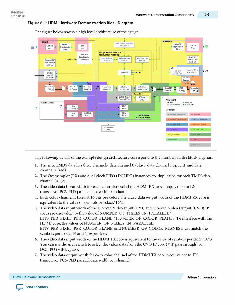
Figure 6-1: HDMI Hardware Demonstration Block Diagram
The figure below shows a high level architecture of the design.
RX TDMS Clock
TX Transceiver Reference Clock
TX Transceiver Clock Out
TX Link Speed Clock
TX Video Clock
I C Clock
Memory Clock
RX Transceiver Reference Clock
RX Transceiver Recovered Clock
RX Link Speed Clock
RX Video Clock
Management Clock
VIP Main Clock 2
Sink DDC and SCDC
Altera PLLIP Core
Altera PLLReconfiguration
IP Core
Transceiver PHYReset Controller
(RX) IP Core
Transceiver Native PHY(RX) IP Core
Oversampler(RX)
HDMI Source
Avalon-MM MasterTranslator
(14)
Qsys System (HDMI Source, SCDC Control, and VIP Passthrough)
Avalon-MM SlaveTranslator
Avalon-MM SlaveTranslator
Nios II CPU
Video FrameBuffer IP Core
Clocked VideoInput IP Core
Clocked VideoOutput IP Core
External MemoryController IP Core
Transceiver ReconfigurationController IP Core
External Memory(DDR3)
VIP Bypass and Audio/Aux/IF Buffers
Source SCDC
Altera HDMIIP Core (TX)
(15)
(5) (6) (7)
Clock EnableGenerator
Transceiver NativePHY (TX) IP Core
Transceiver fPLL IP Core
(2)DCFIFOIP Core (2)
Altera HDMIIP Core (RX)
RateDetect
Multi-RateReconfigurationController (RX)(13)
(1)
(3)(12)
HDMI Sink
I2C Slave(SCDC) (16)
I2C Slave(EDID)
RAM 1-PortIP Core
I2C Master(SCDC)
DCFIFOIP Core
DCFIFOIP Core
DCFIFOIP Core (8)
Oversampler(TX) (8)
(9)
Transceiver PHYReset Controller
(TX) IP Core
Altera PLLReconfiguration
IP Core
Altera PLLIP Core
(10)
(15)
(11)
(5)(4)
DataAvalon-ST Video
Avalon-MMControl/Status
Arrow Legend
Clock Legend
The following details of the example design architecture correspond to the numbers in the block diagram.
1. The sink TMDS data has three channels: data channel 0 (blue), data channel 1 (green), and datachannel 2 (red).
2. The Oversampler (RX) and dual-clock FIFO (DCFIFO) instances are duplicated for each TMDS datachannel (0,1,2).
3. The video data input width for each color channel of the HDMI RX core is equivalent to RXtransceiver PCS-PLD parallel data width per channel.
4. Each color channel is fixed at 16 bits per color. The video data output width of the HDMI RX core isequivalent to the value of symbols per clock*16*3.
5. The video data input width of the Clocked Video Input (CVI) and Clocked Video Output (CVO) IPcores are equivalent to the value of NUMBER_OF_PIXELS_IN_PARALLEL *BITS_PER_PIXEL_PER_COLOR_PLANE * NUMBER_OF_COLOR_PLANES. To interface with theHDMI core, the values of NUMBER_OF_PIXELS_IN_PARALLEL,BITS_PER_PIXEL_PER_COLOR_PLANE, and NUMBER_OF_COLOR_PLANES must match thesymbols per clock, 16 and 3 respectively.
6. The video data input width of the HDMI TX core is equivalent to the value of symbols per clock*16*3.You can use the user switch to select the video data from the CVO IP core (VIP passthrough) orDCFIFO (VIP bypass).
7. The video data output width for each color channel of the HDMI TX core is equivalent to TXtransceiver PCS-PLD parallel data width per channel.
UG-HDMI2016.05.02 Hardware Demonstration Components 6-3
HDMI Hardware Demonstration Altera Corporation
Send Feedback

8. The DCFIFO and the Oversampler (TX) instances are duplicated for each TMDS data channel (0,1,2)and clock channel.
9. The Oversampler (TX) uses the clock enable signal to read data from the DCFIFO.10.The source TMDS data has four channels: data channel 0 (blue), data channel 1 (green), data channel 2
(red), and clock channel.11.The Transceiver fPLL IP Core is instantiated externally to the TX transceiver in Arria 10 devices. The
transceiver PLL is embedded within the TX transceiver in Arria V and Stratix V devices.12.The RX Multirate Reconfiguration Controller requires the status of TMDS_Bit_clock_ Ratio port to
perform appropriate RX reconfiguration between the TMDS character rates below 340 Mcsc (HDMI1.4b) and above 340 Mcsc (HDMI 2.0). The status of the port is also required by the Nios II processorand the HDMI TX core to perform appropriate TX reconfiguration and scrambling.
13.The reset control signals for and lock status signals from HDMI PLL, RX Transceiver Reset Controllerand HDMI RX core.
14.The reset and oversampling control signals for HDMI PLL, TX Transceiver Reset Controller, andHDMI TX core. The lock status and rate detection measure valid signals from the HDMI sink initiatethe TX reconfiguration process.
15.The I2C SCL and SDA lines with tristate buffer for bidirectional configuration. Use Altera GPIO IPcore for Arria 10 devices and ALTIOBUF IP core for Arria V and Stratix V devices.
16.The SCDC is mainly designed for the source to update the TMDS_Bit_Clock_Ratio andScrambler_Enable bits of the sink TMDS Configuration register. The HDMI RX core does notsupport SCDC read request feature for this release.
Transceiver Native PHY (RX)—Arria V and Stratix V Devices• Transceiver Native PHY in Arria V devices
• To operate the TMDS bit rate up to 3,400 Mbps, configure the Transceiver Native PHY at 20 bits atPCS – PLD interface with the HDMI RX core at 2 symbols per clock. When the PCS – PLDinterface width is 20 bits, the minimum link rate is 611 Mbps.
• To operate the TMDS bit rate up to 6,000 Mbps, configure the Transceiver Native PHY at 40 bitswith the HDMI RX core at 4 symbols per clock. When the PCS – PLD interface width is 40 bits, theminimum link rate is 1,000 Mbps.
• Oversampling is required for TMDS bit rate which is below the minimum link rate.• Transceiver Native PHY in Stratix V devices
• To operate the TMDS bit rate up to 6,000 Mbps, configure the Transceiver Native PHY at 20 bits atPCS – PLD interface with the HDMI RX core at 2 symbols per clock. When the PCS – PLDinterface width is 20 bits, the minimum link rate is 611 Mbps.
Table 6-1: Arria V and Stratix V Transceiver Native PHY (RX) Configuration Settings (6,000 Mbps)
This table shows an example of Arria V and Stratix V Transceiver Native PHY (RX) configuration settings forTMDS bit rate of 6,000 Mbps.
Parameters Settings
Datapath Options
Enable TX datapath Off
Enable RX datapath On
6-4 Transceiver Native PHY (RX)—Arria V and Stratix V DevicesUG-HDMI
2016.05.02
Altera Corporation HDMI Hardware Demonstration
Send Feedback

Parameters Settings
Datapath Options
Enable Standard PCS On
Initial PCS datapath selection Standard
Number of data channels 3
Enable simplified data interface On
RX PMA
Data rate 6,000 Mbps
Enable CDR dynamic reconfiguration On
Number of CDR reference clocks 2 (1)
Selected CDR reference clock 0 (1)
Selected CDR reference clock frequency 600 MHz
PPM detector threshold 1,000 PPM
Enable rx_pma_clkout port On
Enable rx_is_lockedtodata port On
Enable rx_is_lockedtoref port On
Enable rx_set_locktodata and rx_set_locktorefports On
Standard PCS
Standard PCS protocol Basic
Standard PCS/PMA interface width • 10 (for 1 symbol per clock)• 20 (for 2 and 4 symbols per clock)
Enable RX byte deserializer • Off (for 1 and 2 symbols per clock)• On (for 4 symbols per clock)
(1) The Bitec HDMI 2.0 HSMC daughter card routes the TMDS clock pin to the transceiver serial data pin. Touse the TMDS clock to drive the HDMI PLL, the TMDS clock must also drive the transceiver dedicatedreference clock pin. The number of CDR reference clocks is 2 with reference clock 1 (unused) driven by theTMDS clock and reference clock 0 driven by the HDMI PLL output clock. The selected CDR reference clockwill be fixed at 0.
UG-HDMI2016.05.02 Transceiver Native PHY (RX)—Arria V and Stratix V Devices 6-5
HDMI Hardware Demonstration Altera Corporation
Send Feedback
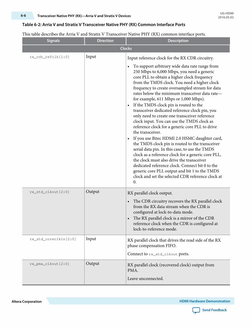
Table 6-2: Arria V and Stratix V Transceiver Native PHY (RX) Common Interface Ports
This table describes the Arria V and Stratix V Transceiver Native PHY (RX) common interface ports.Signals Direction Description
Clocks
rx_cdr_refclk[1:0] Input Input reference clock for the RX CDR circuitry.
• To support arbitrary wide data rate range from250 Mbps to 6,000 Mbps, you need a genericcore PLL to obtain a higher clock frequencyfrom the TMDS clock. You need a higher clockfrequency to create oversampled stream for datarates below the minimum transceiver data rate—for example, 611 Mbps or 1,000 Mbps).
• If the TMDS clock pin is routed to thetransceiver dedicated reference clock pin, youonly need to create one transceiver referenceclock input. You can use the TMDS clock asreference clock for a generic core PLL to drivethe transceiver.
• If you use Bitec HDMI 2.0 HSMC daughter card,the TMDS clock pin is routed to the transceiverserial data pin. In this case, to use the TMDSclock as a reference clock for a generic core PLL,the clock must also drive the transceiverdedicated reference clock. Connect bit 0 to thegeneric core PLL output and bit 1 to the TMDSclock and set the selected CDR reference clock at0.
rx_std_clkout[2:0] Output RX parallel clock output.
• The CDR circuitry recovers the RX parallel clockfrom the RX data stream when the CDR isconfigured at lock-to-data mode.
• The RX parallel clock is a mirror of the CDRreference clock when the CDR is configured atlock-to-reference mode.
rx_std_coreclkin[2:0] Input RX parallel clock that drives the read side of the RXphase compensation FIFO.
Connect to rx_std_clkout ports.
rx_pma_clkout[2:0] Output RX parallel clock (recovered clock) output fromPMA.
Leave unconnected.
6-6 Transceiver Native PHY (RX)—Arria V and Stratix V DevicesUG-HDMI
2016.05.02
Altera Corporation HDMI Hardware Demonstration
Send Feedback
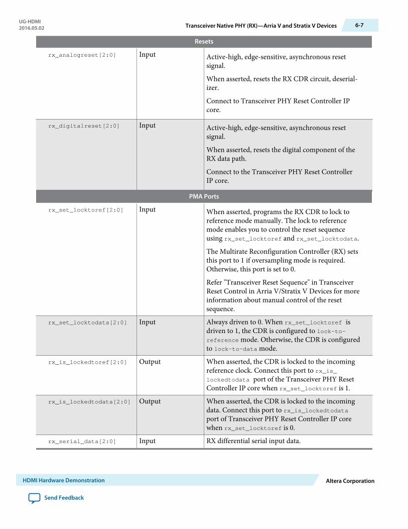
Resets
rx_analogreset[2:0] Input Active-high, edge-sensitive, asynchronous resetsignal.
When asserted, resets the RX CDR circuit, deserial‐izer.
Connect to Transceiver PHY Reset Controller IPcore.
rx_digitalreset[2:0] Input Active-high, edge-sensitive, asynchronous resetsignal.
When asserted, resets the digital component of theRX data path.
Connect to the Transceiver PHY Reset ControllerIP core.
PMA Ports
rx_set_locktoref[2:0] Input When asserted, programs the RX CDR to lock toreference mode manually. The lock to referencemode enables you to control the reset sequenceusing rx_set_locktoref and rx_set_locktodata.
The Multirate Reconfiguration Controller (RX) setsthis port to 1 if oversampling mode is required.Otherwise, this port is set to 0.
Refer "Transceiver Reset Sequence" in TransceiverReset Control in Arria V/Stratix V Devices for moreinformation about manual control of the resetsequence.
rx_set_locktodata[2:0] Input Always driven to 0. When rx_set_locktoref isdriven to 1, the CDR is configured to lock-to-reference mode. Otherwise, the CDR is configuredto lock-to-data mode.
rx_is_lockedtoref[2:0] Output When asserted, the CDR is locked to the incomingreference clock. Connect this port to rx_is_lockedtodata port of the Transceiver PHY ResetController IP core when rx_set_locktoref is 1.
rx_is_lockedtodata[2:0] Output When asserted, the CDR is locked to the incomingdata. Connect this port to rx_is_lockedtodataport of Transceiver PHY Reset Controller IP corewhen rx_set_locktoref is 0.
rx_serial_data[2:0] Input RX differential serial input data.
UG-HDMI2016.05.02 Transceiver Native PHY (RX)—Arria V and Stratix V Devices 6-7
HDMI Hardware Demonstration Altera Corporation
Send Feedback
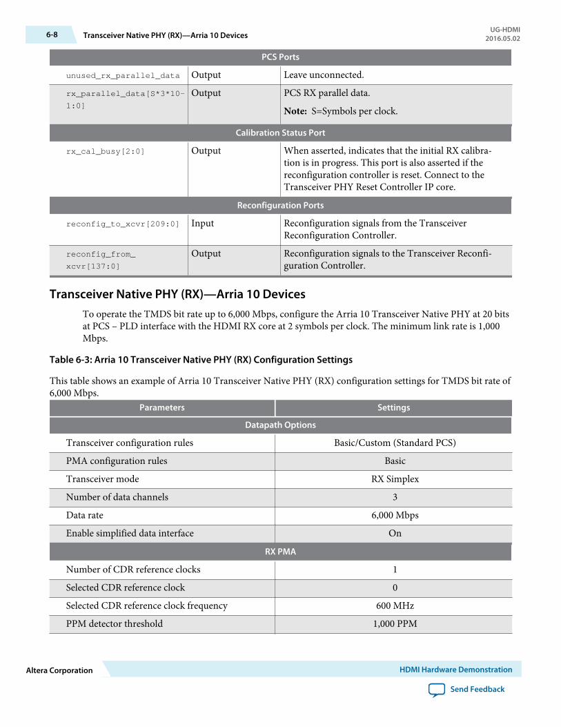
PCS Ports
unused_rx_parallel_data Output Leave unconnected.
rx_parallel_data[S*3*10-
1:0]
Output PCS RX parallel data.
Note: S=Symbols per clock.
Calibration Status Port
rx_cal_busy[2:0] Output When asserted, indicates that the initial RX calibra‐tion is in progress. This port is also asserted if thereconfiguration controller is reset. Connect to theTransceiver PHY Reset Controller IP core.
Reconfiguration Ports
reconfig_to_xcvr[209:0] Input Reconfiguration signals from the TransceiverReconfiguration Controller.
reconfig_from_
xcvr[137:0]
Output Reconfiguration signals to the Transceiver Reconfi‐guration Controller.
Transceiver Native PHY (RX)—Arria 10 DevicesTo operate the TMDS bit rate up to 6,000 Mbps, configure the Arria 10 Transceiver Native PHY at 20 bitsat PCS – PLD interface with the HDMI RX core at 2 symbols per clock. The minimum link rate is 1,000Mbps.
Table 6-3: Arria 10 Transceiver Native PHY (RX) Configuration Settings
This table shows an example of Arria 10 Transceiver Native PHY (RX) configuration settings for TMDS bit rate of6,000 Mbps.
Parameters Settings
Datapath Options
Transceiver configuration rules Basic/Custom (Standard PCS)
PMA configuration rules Basic
Transceiver mode RX Simplex
Number of data channels 3
Data rate 6,000 Mbps
Enable simplified data interface On
RX PMA
Number of CDR reference clocks 1
Selected CDR reference clock 0
Selected CDR reference clock frequency 600 MHz
PPM detector threshold 1,000 PPM
6-8 Transceiver Native PHY (RX)—Arria 10 DevicesUG-HDMI
2016.05.02
Altera Corporation HDMI Hardware Demonstration
Send Feedback
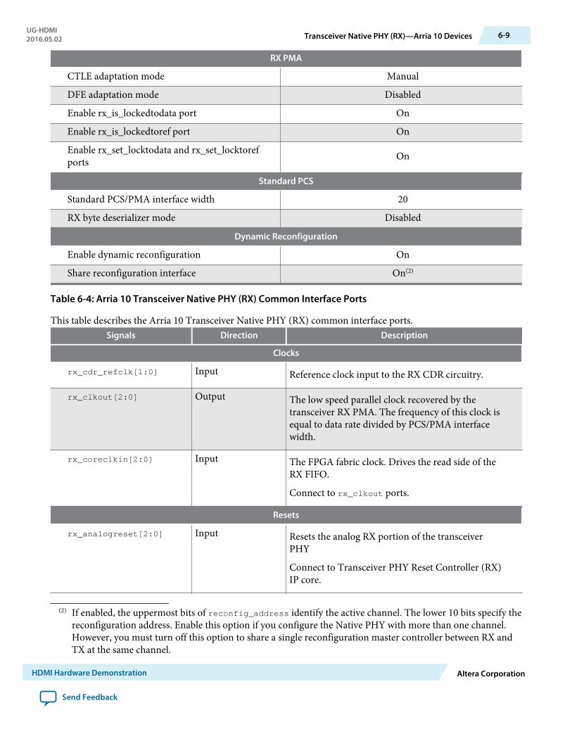
RX PMA
CTLE adaptation mode Manual
DFE adaptation mode Disabled
Enable rx_is_lockedtodata port On
Enable rx_is_lockedtoref port On
Enable rx_set_locktodata and rx_set_locktorefports On
Standard PCS
Standard PCS/PMA interface width 20
RX byte deserializer mode Disabled
Dynamic Reconfiguration
Enable dynamic reconfiguration On
Share reconfiguration interface On(2)
Table 6-4: Arria 10 Transceiver Native PHY (RX) Common Interface Ports
This table describes the Arria 10 Transceiver Native PHY (RX) common interface ports.Signals Direction Description
Clocks
rx_cdr_refclk[1:0] Input Reference clock input to the RX CDR circuitry.
rx_clkout[2:0] Output The low speed parallel clock recovered by thetransceiver RX PMA. The frequency of this clock isequal to data rate divided by PCS/PMA interfacewidth.
rx_coreclkin[2:0] Input The FPGA fabric clock. Drives the read side of theRX FIFO.
Connect to rx_clkout ports.
Resets
rx_analogreset[2:0] Input Resets the analog RX portion of the transceiverPHY
Connect to Transceiver PHY Reset Controller (RX)IP core.
(2) If enabled, the uppermost bits of reconfig_address identify the active channel. The lower 10 bits specify thereconfiguration address. Enable this option if you configure the Native PHY with more than one channel.However, you must turn off this option to share a single reconfiguration master controller between RX andTX at the same channel.
UG-HDMI2016.05.02 Transceiver Native PHY (RX)—Arria 10 Devices 6-9
HDMI Hardware Demonstration Altera Corporation
Send Feedback

Resets
rx_digitalreset[2:0] Input Resets the digital RX portion of the transceiverPHY.
Connect to the Transceiver PHY Reset Controller(RX) IP core.
PMA Ports
rx_set_locktoref[2:0] Input This port provides manual control of the RX CDRcircuitry.
The Multirate Reconfiguration Controller (RX) setsthis port to 1 if oversampling mode is required.Otherwise, this port is set to 0.
rx_set_locktodata[2:0] Input Always driven to 0. When rx_set_locktoref isdriven to 1, the CDR is configured to lock-to-reference mode. Otherwise, the CDR is configuredto lock-to-data mode.
rx_is_lockedtoref[2:0] Output When asserted, the CDR is locked to the incomingreference clock. Connect this port to rx_is_lockedtodata port of the Transceiver PHY ResetController IP core when rx_set_locktoref is 1.
rx_is_lockedtodata[2:0] Output When asserted, the CDR is locked to the incomingdata. Connect this port to rx_is_lockedtodataport of Transceiver PHY Reset Controller IP corewhen rx_set_locktoref is 0.
rx_serial_data[2:0] Input RX differential serial input data.
PCS Ports
unused_rx_parallel_data Output Leave unconnected.
rx_parallel_data[S*3*10-
1:0]
Output PCS RX parallel data.
Note: S=Symbols per clock.
Calibration Status Port
rx_cal_busy[2:0] Output When asserted, indicates that the initial RX calibra‐tion is in progress. For both initial and manualrecalibrations, this signal asserts during calibrationand deasserts after calibration is completed.Connect to the Transceiver PHY Reset ControllerIP core.
Avalon-MM Control Ports
reconfig_clk Input Avalon clock. The clock frequency is 100–125 MHz.
reconfig_reset Input Resets the Avalon interface.
6-10 Transceiver Native PHY (RX)—Arria 10 DevicesUG-HDMI
2016.05.02
Altera Corporation HDMI Hardware Demonstration
Send Feedback
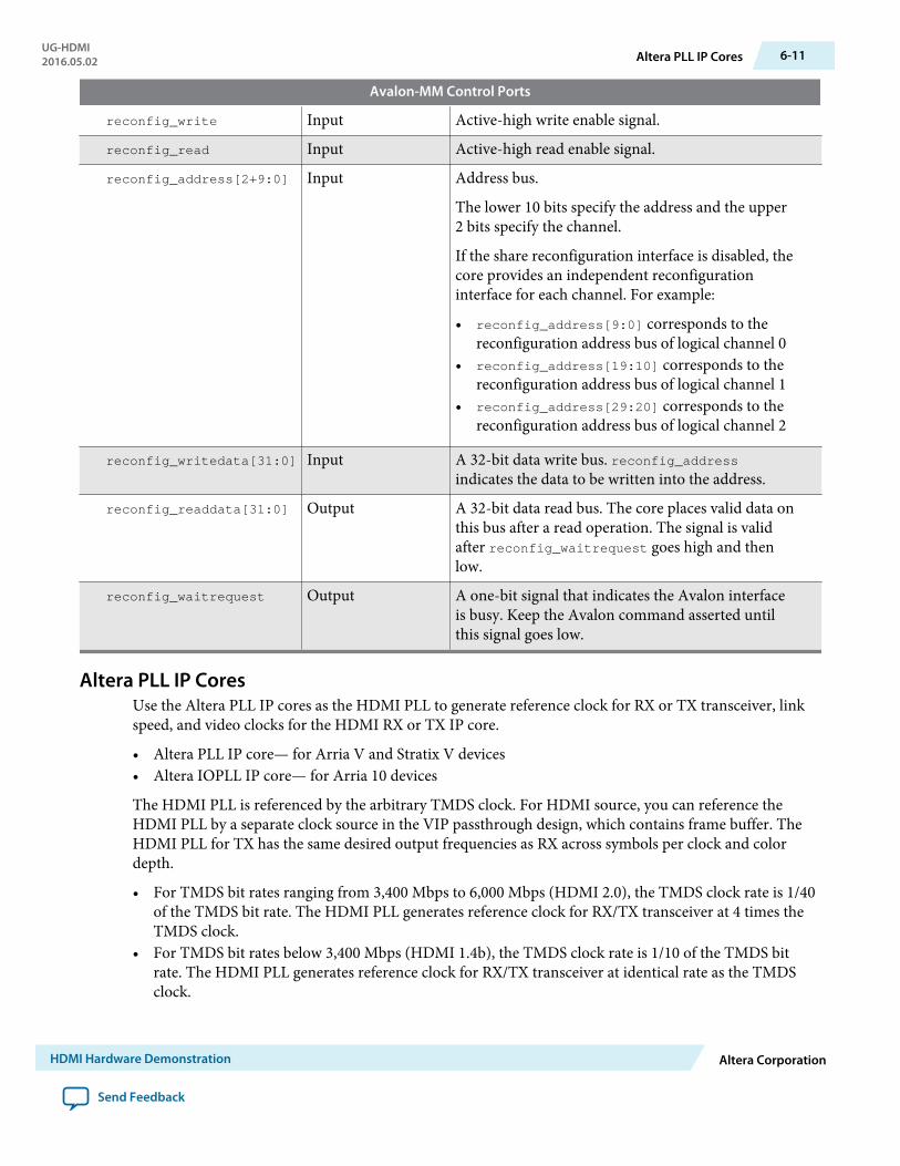
Avalon-MM Control Ports
reconfig_write Input Active-high write enable signal.
reconfig_read Input Active-high read enable signal.
reconfig_address[2+9:0] Input Address bus.
The lower 10 bits specify the address and the upper2 bits specify the channel.
If the share reconfiguration interface is disabled, thecore provides an independent reconfigurationinterface for each channel. For example:
• reconfig_address[9:0] corresponds to thereconfiguration address bus of logical channel 0
• reconfig_address[19:10] corresponds to thereconfiguration address bus of logical channel 1
• reconfig_address[29:20] corresponds to thereconfiguration address bus of logical channel 2
reconfig_writedata[31:0] Input A 32-bit data write bus. reconfig_addressindicates the data to be written into the address.
reconfig_readdata[31:0] Output A 32-bit data read bus. The core places valid data onthis bus after a read operation. The signal is validafter reconfig_waitrequest goes high and thenlow.
reconfig_waitrequest Output A one-bit signal that indicates the Avalon interfaceis busy. Keep the Avalon command asserted untilthis signal goes low.
Altera PLL IP CoresUse the Altera PLL IP cores as the HDMI PLL to generate reference clock for RX or TX transceiver, linkspeed, and video clocks for the HDMI RX or TX IP core.
• Altera PLL IP core— for Arria V and Stratix V devices• Altera IOPLL IP core— for Arria 10 devices
The HDMI PLL is referenced by the arbitrary TMDS clock. For HDMI source, you can reference theHDMI PLL by a separate clock source in the VIP passthrough design, which contains frame buffer. TheHDMI PLL for TX has the same desired output frequencies as RX across symbols per clock and colordepth.
• For TMDS bit rates ranging from 3,400 Mbps to 6,000 Mbps (HDMI 2.0), the TMDS clock rate is 1/40of the TMDS bit rate. The HDMI PLL generates reference clock for RX/TX transceiver at 4 times theTMDS clock.
• For TMDS bit rates below 3,400 Mbps (HDMI 1.4b), the TMDS clock rate is 1/10 of the TMDS bitrate. The HDMI PLL generates reference clock for RX/TX transceiver at identical rate as the TMDSclock.
UG-HDMI2016.05.02 Altera PLL IP Cores 6-11
HDMI Hardware Demonstration Altera Corporation
Send Feedback

If the TMDS link operates at TMDS bit rates below the minimum RX/TX transceiver link rate, yourdesign requires oversampling and a factor of 5 is chosen. The minimum link rate of the RX/TX transceivervary across device families and symbols per clock. The HDMI PLL generates reference clock for RX/TXtransceiver at 5 times the TMDS clock.
Note: Place the Altera PLL in the transmit path (pll_hdmi_tx) in the physical location next to thetransceiver PLL.
Table 6-5: HDMI PLL Desired Output Frequencies for 8-bpc Video
This table shows an example of HDMI PLL desired output frequencies across various TMDS clock rates andsymbols per clock for all supported device families using 8-bpc video.
DeviceFamily
SymbolsPer
Clock
MinimumLink Rate
(Mbps)
TMDS BitRate
(Mbps)
Oversam‐pling (5x)Required
TMDSClock Rate
(MHz)
RX/TXTransceive
r Refclk(MHz)
RX/TX LinkSpeedClock(MHz)
RX/TX VideoClock (MHz)
Arria 10 2 1,000
250 Yes 25 100 12.5 12.5
1,080 No 108 108 54 54
2,967 No 296.7 296.7 148.35 148.35
5,940 No 148.5 594 297 297
Arria V
2 611
270 Yes 27 135 13.5 13.5
742.5 No 74.25 74.25 37.125 37.125
1,485 No 148.5 148.5 74.25 74.25
2,970 No 297 297 148.5 148.5
4 1,000
270 Yes 27 135 6.75 6.75
742.5 Yes 74.25 371.25 18.5625 18.5625
1,485 No 148.5 148.5 37.125 37.125
5,940 No 148.5 594 148.5 148.5
Stratix V 2 611
540 Yes 54 270 27 27
1,620 No 162 162 81 81
5,934 No 296.7 593.4 296.7 296.7
The color depths greater than 8 bpc or 24 bpp are defined to be deep color. For a color depth of 8 bpc, thecore carries the pixels at a rate of one pixel per TMDS clock. At deeper color depths, the TMDS clock runsfaster than the source pixel clock to provide the extra bandwidth for the additional bits.
The TMDS clock rate is increased by the ratio of the pixel size to 8 bits:
• 8 bits mode—TMDS clock = 1.0 × pixel or video clock (1:1)• 10 bits mode—TMDS clock = 1.25 × pixel or video clock (5:4)• 12 bits mode—TMDS clock = 1.5 × pixel or video clock (3:2)• 16 bits mode—TMDS clock = 2 × pixel or video clock (2:1)
6-12 Altera PLL IP CoresUG-HDMI
2016.05.02
Altera Corporation HDMI Hardware Demonstration
Send Feedback
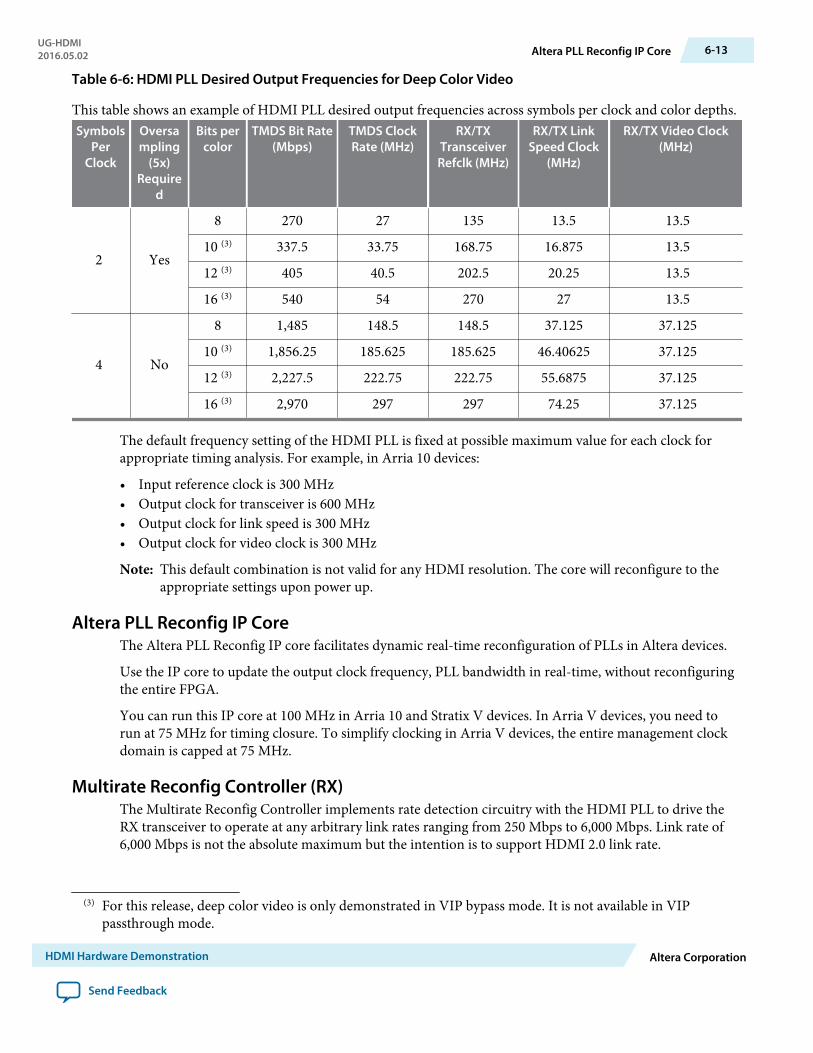
Table 6-6: HDMI PLL Desired Output Frequencies for Deep Color Video
This table shows an example of HDMI PLL desired output frequencies across symbols per clock and color depths.Symbols
PerClock
Oversampling
(5x)Require
d
Bits percolor
TMDS Bit Rate(Mbps)
TMDS ClockRate (MHz)
RX/TXTransceiverRefclk (MHz)
RX/TX LinkSpeed Clock
(MHz)
RX/TX Video Clock(MHz)
2 Yes
8 270 27 135 13.5 13.5
10 (3) 337.5 33.75 168.75 16.875 13.5
12 (3) 405 40.5 202.5 20.25 13.5
16 (3) 540 54 270 27 13.5
4 No
8 1,485 148.5 148.5 37.125 37.125
10 (3) 1,856.25 185.625 185.625 46.40625 37.125
12 (3) 2,227.5 222.75 222.75 55.6875 37.125
16 (3) 2,970 297 297 74.25 37.125
The default frequency setting of the HDMI PLL is fixed at possible maximum value for each clock forappropriate timing analysis. For example, in Arria 10 devices:
• Input reference clock is 300 MHz• Output clock for transceiver is 600 MHz• Output clock for link speed is 300 MHz• Output clock for video clock is 300 MHz
Note: This default combination is not valid for any HDMI resolution. The core will reconfigure to theappropriate settings upon power up.
Altera PLL Reconfig IP CoreThe Altera PLL Reconfig IP core facilitates dynamic real-time reconfiguration of PLLs in Altera devices.
Use the IP core to update the output clock frequency, PLL bandwidth in real-time, without reconfiguringthe entire FPGA.
You can run this IP core at 100 MHz in Arria 10 and Stratix V devices. In Arria V devices, you need torun at 75 MHz for timing closure. To simplify clocking in Arria V devices, the entire management clockdomain is capped at 75 MHz.
Multirate Reconfig Controller (RX)The Multirate Reconfig Controller implements rate detection circuitry with the HDMI PLL to drive theRX transceiver to operate at any arbitrary link rates ranging from 250 Mbps to 6,000 Mbps. Link rate of6,000 Mbps is not the absolute maximum but the intention is to support HDMI 2.0 link rate.
(3) For this release, deep color video is only demonstrated in VIP bypass mode. It is not available in VIPpassthrough mode.
UG-HDMI2016.05.02 Altera PLL Reconfig IP Core 6-13
HDMI Hardware Demonstration Altera Corporation
Send Feedback
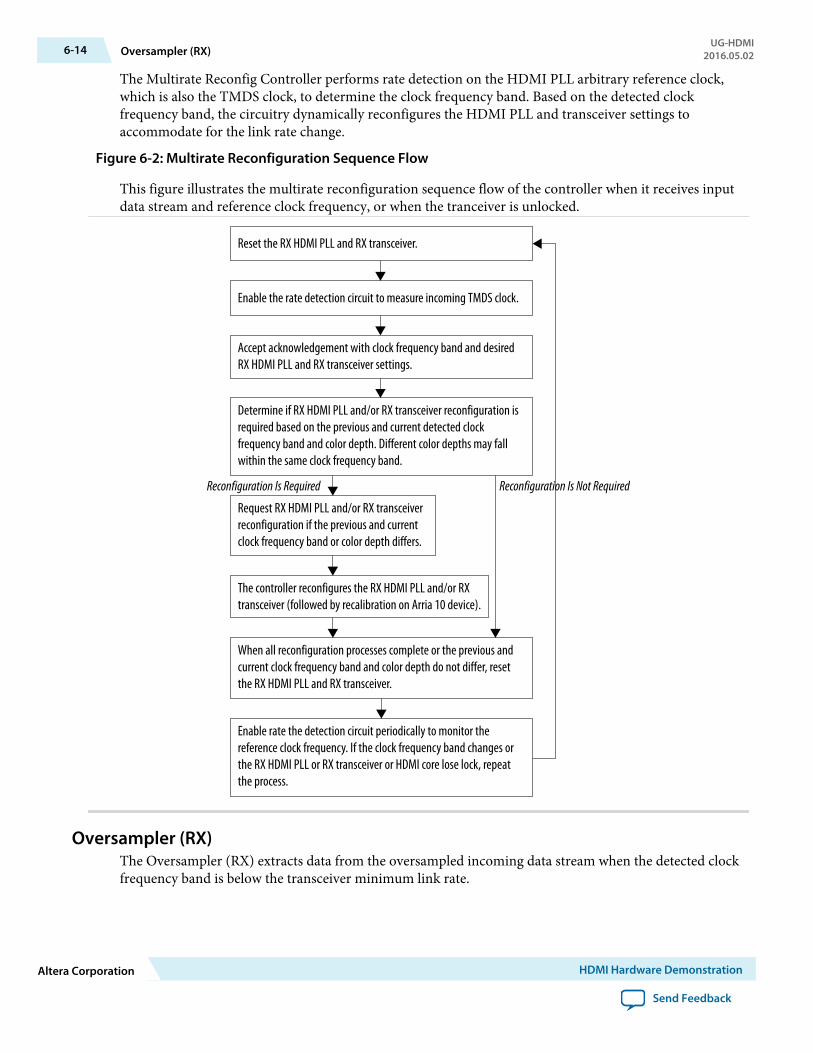
The Multirate Reconfig Controller performs rate detection on the HDMI PLL arbitrary reference clock,which is also the TMDS clock, to determine the clock frequency band. Based on the detected clockfrequency band, the circuitry dynamically reconfigures the HDMI PLL and transceiver settings toaccommodate for the link rate change.
Figure 6-2: Multirate Reconfiguration Sequence Flow
This figure illustrates the multirate reconfiguration sequence flow of the controller when it receives inputdata stream and reference clock frequency, or when the tranceiver is unlocked.
Reset the RX HDMI PLL and RX transceiver.
Enable the rate detection circuit to measure incoming TMDS clock.
Accept acknowledgement with clock frequency band and desired RX HDMI PLL and RX transceiver settings.
Determine if RX HDMI PLL and/or RX transceiver reconfiguration is required based on the previous and current detected clock frequency band and color depth. Different color depths may fall within the same clock frequency band.
Request RX HDMI PLL and/or RX transceiver reconfiguration if the previous and current clock frequency band or color depth differs.
The controller reconfigures the RX HDMI PLL and/or RX transceiver (followed by recalibration on Arria 10 device).
When all reconfiguration processes complete or the previous and current clock frequency band and color depth do not differ, reset the RX HDMI PLL and RX transceiver.
Enable rate the detection circuit periodically to monitor the reference clock frequency. If the clock frequency band changes or the RX HDMI PLL or RX transceiver or HDMI core lose lock, repeat the process.
Reconfiguration Is Required Reconfiguration Is Not Required
Oversampler (RX)The Oversampler (RX) extracts data from the oversampled incoming data stream when the detected clockfrequency band is below the transceiver minimum link rate.
6-14 Oversampler (RX)UG-HDMI
2016.05.02
Altera Corporation HDMI Hardware Demonstration
Send Feedback
The oversampling factor is fixed at 5 and you can program the data width to support different number ofsymbols. The supported data width is 20 bit for 2 symbols per clock and 40 bits for 4 symbols per clock.The extracted bit will be accompanied by data valid pulse which asserts every 5 clock cycles.
DCFIFOThe DCFIFO transfers data from the RX transceiver recovered clock domain to the RX link speed clockdomain. The DCFIFO transfers data from the TX link speed clock domain to the TX transceiver parallelclock out domain.
• Sink
• When the Multirate Reconfig Controller (RX) detects an incoming input stream that is below thetransceiver minimum link rate, the DCFIFO accepts the data from the Oversampler with data validpulse as write request asserted every 5 clock cycles.
• Otherwise, it accepts data directly from the transceiver with write request asserted at all times.• Source
• When Nios II processor determines the outgoing data stream is below the TX transceiver minimumlink rate, the TX transceiver accepts the data from the Oversampler (TX).
• Otherwise, the TX transceiver reads data directly from the DCFIFO with read request asserted at alltimes.
Sink Display Data Channel (DDC) & Status and Control Data Channel (SCDC)The HDMI source uses the DDC to determine the capabilities and characteristics of the sink by readingthe Enhanced Extended Display Identification Data (E-EDID) data structure.
The E-EDID memory is stored using the RAM 1-Port IP core. A standard two-wire (clock and data) serialdata bus protocol (I2C slave-only controller) is used to transfer CEA-861-D compliant E-EDID datastructure.
The 8-bit I2C slave addresses for the E-EDID are 0xA0/0xA1. The LSB indicates the access type: 1 for readand 0 for write. When an HPD event occurs, the I2C slave responds to E-EDID data by reading from theRAM.
The I2C slave-only controller is also used to support SCDC for HDMI 2.0 operation. The 8-bit I2C slaveaddresses for the SCDC are 0xA8/0xA9. When an HPD event occurs, the I2C slave performs write/readtransaction to/from SCDC interface of HDMI RX core. This I2C slave-only controller for SCDC is notrequired if HDMI 2.0 is not intended.
Transceiver Reconfiguration ControllerYou can use the Transceiver Reconfiguration Controller IP core to change the device transceiver settingsat any time.
You can selectively reconfigure any portion of the transceiver. The reconfiguration of each portionrequires a read-modify-write operation (read first, then write). The read-modify-write operation modifiesonly the appropriate bits in a register and does not affect the other bits.
The Transceiver Reconfiguration Controller is only available and required in Arria V and Stratix Vdevices. Because the RX and TX transceivers share a single controller, the controller requires Qsysinterconnects, such as Avalon-MM Master Translator and Avalon-MM Slave Translator, in the Qsyssystem.
UG-HDMI2016.05.02 DCFIFO 6-15
HDMI Hardware Demonstration Altera Corporation
Send Feedback
• The Avalon-MM Master Translator provides an interface between this controller and the RX MultirateReconfig Controller.
• The Avalon-MM Slave Translator arbitrates the RX and TX reconfiguration event for this controller.
In Arria 10 devices, the Transceiver Native PHY has a direct access the Avalon-MM reconfigurationinterface.
• The RX Multirate Reconfig Controller directly drives the RX transceiver reconfiguration interface.• The Avalon-MM Slave Translator converts the Nios II reconfiguration command and directly drives
the TX transceiver reconfiguration interface.
VIP Bypass and Audio, Auxiliary and InfoFrame BuffersThe video data output and synchronization signals from HDMI RX core is looped through a DCFIFOacross RX and TX video clock domains. The General Control Packet (GCP), InfoFrames (AVI, VSI, andAI), auxiliary data and audio data are looped through DCFIFOs across RX and TX link speed clockdomains.
The auxiliary data port of the HDMI TX core controls the auxiliary data that flow through DCFIFOthrough backpressure. The backpressure ensures there is no incomplete auxiliary packet on the auxiliarydata port. This block also performs external filtering on the audio data and audio clock regenerationpacket from the auxiliary data stream before sending to the HDMI TX core auxiliary data port.
Transceiver Native PHY (TX)—Arria V and Stratix V DevicesThe Arria V and Stratix V Transceiver Native PHY (TX) configuration settings are typically the same asRX.
Table 6-7: Arria V and Stratix V Transceiver Native PHY (TX) Configuration Settings (6,000 Mbps)
This table shows an example of Arria V and Stratix V Transceiver Native PHY (TX) configuration settings forTMDS bit rate of 6,000 Mbps.
Parameters Settings
Datapath Options
Enable TX datapath On
Enable RX datapath Off
Enable Standard PCS On
Initial PCS datapath selection Standard
Number of data channels 4
Bonding mode xN
Enable simplified data interface On
TX PMA
Data rate 6,000 Mbps
TX local clock division factor 1
Enable TX PLL dynamic reconfiguration On
6-16 VIP Bypass and Audio, Auxiliary and InfoFrame BuffersUG-HDMI
2016.05.02
Altera Corporation HDMI Hardware Demonstration
Send Feedback

TX PMA
Use external TX PLL Off
Number of TX PLLs 1
Main TX PLL logical index 0
Number of TX PLL reference clocks 1
PLL type CMU
Reference clock frequency 600 MHz
Selected reference clock source 0
Selected clock network xN
Standard PCS
Standard PCS protocol Basic
Standard PCS/PMA interface width • 10 (for 1 symbol per clock)• 20 (for 2 and 4 symbols per clock)
Enable TX byte serializer • Off (for 1 and 2 symbols per clock)• On (for 4 symbols per clock)
Table 6-8: Arria V and Stratix V Transceiver Native PHY (TX) Common Interface Ports
This table describes the Arria V and Stratix V Transceiver Native PHY (TX) common interface ports.Signals Direction Description
Clocks
tx_pll_refclk Input The reference clock input to the TX PLL.
tx_std_clkout[3:0] Output TX parallel clock output.
tx_std_coreclkin[3:0] Input TX parallel clock that drives the write side of the TXphase compensation FIFO.
Connect to tx_std_clkout[0] ports.
Resets
tx_analogreset[3:0] Input When asserted, resets all the blocks in TX PMA.
Connect to Transceiver PHY Reset Controller (TX)IP core.
tx_digitalreset[3:0] Input When asserted, resets all the blocks in TX PCS.
Connect to the Transceiver PHY Reset Controller(TX) IP core.
UG-HDMI2016.05.02 Transceiver Native PHY (TX)—Arria V and Stratix V Devices 6-17
HDMI Hardware Demonstration Altera Corporation
Send Feedback

TX PLL
pll_powerdown Input When asserted, resets the TX PLL.
Connect to the Transceiver PHY Reset Controller(TX) IP core.
pll_locked Output When asserted, indicates that the TX PLL is locked.
Connect to the Transceiver PHY Reset Controller(TX) IP core.
PCS Ports
unused_tx_parallel_data Input Leave unconnected.
tx_parallel_data[S*4*10-
1:0]
Input PCS TX parallel data.
Note: S=Symbols per clock.
PMA Port
tx_serial_data[3:0] Output TX differential serial output data.
Calibration Status Port
tx_cal_busy[3:0] Output When asserted, indicates that the initial TX calibra‐tion is in progress. This port is also asserted if thereconfiguration controller is reset. Connect to theTransceiver PHY Reset Controller (TX) IP core.
Reconfiguration Ports
reconfig_to_xcvr[349:0] Input Reconfiguration signals from the TransceiverReconfiguration Controller.
reconfig_from_
xcvr[229:0]
Output Reconfiguration signals to the Transceiver Reconfi‐guration Controller.
Transceiver Native PHY (TX)—Arria 10 DevicesThe Arria 10 Transceiver Native PHY (TX) configuration settings are typically the same as RX.
Table 6-9: Arria 10 Transceiver Native PHY (TX) Configuration Settings
This table shows an example of Arria 10 Transceiver Native PHY (TX) configuration settings for TMDS bit rate of6,000 Mbps.
Parameters Settings
Datapath Options
Transceiver configuration rules Basic/Custom (Standard PCS)
PMA configuration rules Basic
Transceiver mode TX Simplex
6-18 Transceiver Native PHY (TX)—Arria 10 DevicesUG-HDMI
2016.05.02
Altera Corporation HDMI Hardware Demonstration
Send Feedback
Parameters Settings
Datapath Options
Number of data channels 4
Data rate 6,000 Mbps
Enable simplified data interface On
TX PMA
TX channel bonding mode PMA only bonding
Standard PCS
Standard PCS/PMA interface width 20
TX byte serializer mode Disabled
Dynamic Reconfiguration
Enable dynamic reconfiguration Off
Table 6-10: Arria 10 Transceiver Native PHY (TX) Common Interface Ports
This table describes the Arria 10 Transceiver Native PHY (TX) common interface ports.Signals Direction Description
Clocks
tx_bonding_clocks[C*6-
1:0]
Input This is a 6-bit bus which carries the low speedparallel clock per channel. These clocks are outputsfrom the master CGB.
Connect to Transceiver fPLL IP core.
Note: C=Number of transceiver channels (4).
tx_clkout[3:0] Output This is a parallel clock generated by the local CGBfor non-bonded configurations, and by the masterCGB for bonded configurations. The frequency ofthis block is equal to the data rate divided by PCS/PMA interface width.
tx_coreclkin[3:0] Input The FPGA fabric clock. Drives the write side of theTX FIFO.
Connect to tx_clkout[0] ports.
Resets
tx_analogreset[3:0] Input Resets the analog TX portion of the transceiverPHY.
Connect to Transceiver PHY Reset Controller (TX)IP core.
UG-HDMI2016.05.02 Transceiver Native PHY (TX)—Arria 10 Devices 6-19
HDMI Hardware Demonstration Altera Corporation
Send Feedback

Resets
tx_digitalreset[3:0] Input Resets the digital TX portion of the transceiverPHY.
Connect to the Transceiver PHY Reset Controller(TX) IP core.
PCS Ports
unused_tx_parallel_data Input Leave unconnected.
tx_parallel_data[S*4*10-
1:0]
Input PCS TX parallel data.
Note: S=Symbols per clock.
PMA Ports
tx_serial_data[3:0] Output TX differential serial input data.
Calibration Status Port
tx_cal_busy[2:0] Output When asserted, indicates that the initial TX calibra‐tion is in progress. For both initial and manualrecalibrations, this signal asserts during calibrationand deasserts after calibration is completed.Connect to the Transceiver PHY Reset Controller(TX) IP core.
Transceiver PHY Reset ControllerThe Transceiver PHY Reset Controller IP core ensures a reliable initialization of the RX and TXtransceivers.
The reset controller has separate reset controls per channel to handle synchronization of reset inputs,lagging of PLL locked status, and automatic or manual reset recovery mode.
Transceiver fPLL IP CoreIn Arria 10 devices, you instantiate the transceiver PLL externally to the Transceiver Native PHY (TX).The Transceiver fPLL IP core generates the high speed clock required by the transceiver channels.
The master and local clock generation blocks (CGB) provide the necessary high-speed serial and low-speed parallel clocks to drive the non-bonded and bonded channels in the transceiver bank.
Table 6-11: Arria 10 Transceiver fPLL Configuration Settings
This table shows an example of Arria 10 Transceiver fPLL configuration settings for TMDS bit rate of 6,000 Mbps.Parameters Settings
PLL
Protocol mode Basic
Bandwidth Medium
Number of PLL reference clocks 1
6-20 Transceiver PHY Reset ControllerUG-HDMI
2016.05.02
Altera Corporation HDMI Hardware Demonstration
Send Feedback
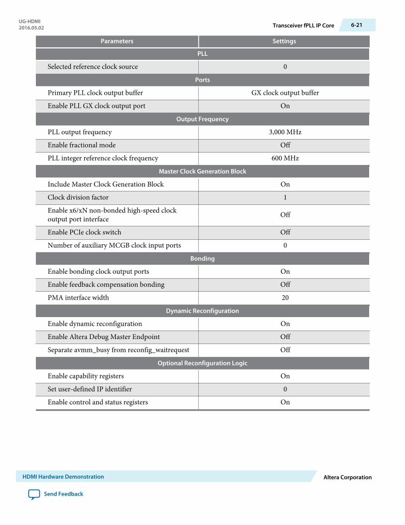
Parameters Settings
PLL
Selected reference clock source 0
Ports
Primary PLL clock output buffer GX clock output buffer
Enable PLL GX clock output port On
Output Frequency
PLL output frequency 3,000 MHz
Enable fractional mode Off
PLL integer reference clock frequency 600 MHz
Master Clock Generation Block
Include Master Clock Generation Block On
Clock division factor 1
Enable x6/xN non-bonded high-speed clockoutput port interface Off
Enable PCIe clock switch Off
Number of auxiliary MCGB clock input ports 0
Bonding
Enable bonding clock output ports On
Enable feedback compensation bonding Off
PMA interface width 20
Dynamic Reconfiguration
Enable dynamic reconfiguration On
Enable Altera Debug Master Endpoint Off
Separate avmm_busy from reconfig_waitrequest Off
Optional Reconfiguration Logic
Enable capability registers On
Set user-defined IP identifier 0
Enable control and status registers On
UG-HDMI2016.05.02 Transceiver fPLL IP Core 6-21
HDMI Hardware Demonstration Altera Corporation
Send Feedback

Table 6-12: Arria 10 Transceiver fPLL Common Interface Ports
This table describes the Arria 10 Transceiver fPLL common interface ports.Signals Direction Description
Clocks
pll_refclk0 Input Reference clock input port 0.
tx_bonding_clocks[C*6-
1:0]
Output 6-bit bus which carries the low speed parallel clockoutputs from master CGB. Each transceiver channelin a bonded group has this 6-bit bus.
Used for channel bonding, and represents the x6/xN clock network.
Connect to Transceiver Native PHY (TX) IP core.
Note: C=Number of transceiver channels (4).
tx_serial_clk Output High speed serial clock output port for GTchannels.
Leave unconnected.
Reset
mcgb_rst Input Master CGB reset control.
Status Ports
pll_powerdown Input When asserted high, resets the PLL.
Connect to Transceiver Reset Controller (TX) IPcore.
pll_cal_busy Output Status signal that asserts high when PLL calibrationis in progress.
OR this signal with tx_cal_busy port beforeconnecting to the Transceiver Reset Controller (TX)IP core.
pll_locked Output Active-high status signal that indicates if the PLL islocked.
Connect to Transceiver Reset Controller (TX) IPcore.
Avalon-MM Control Ports
reconfig_clk0 Input Avalon interface clock.
reconfig_reset0 Input Resets the Avalon interface.
reconfig_write0 Input Active-high write enable signal.
6-22 Transceiver fPLL IP CoreUG-HDMI
2016.05.02
Altera Corporation HDMI Hardware Demonstration
Send Feedback
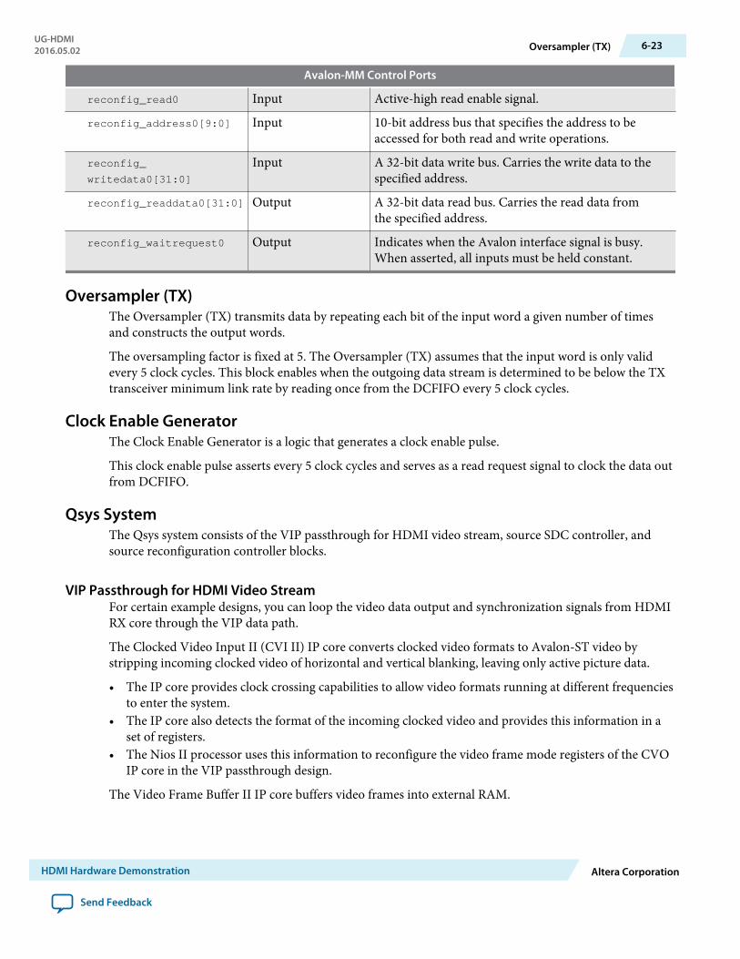
Avalon-MM Control Ports
reconfig_read0 Input Active-high read enable signal.
reconfig_address0[9:0] Input 10-bit address bus that specifies the address to beaccessed for both read and write operations.
reconfig_
writedata0[31:0]
Input A 32-bit data write bus. Carries the write data to thespecified address.
reconfig_readdata0[31:0] Output A 32-bit data read bus. Carries the read data fromthe specified address.
reconfig_waitrequest0 Output Indicates when the Avalon interface signal is busy.When asserted, all inputs must be held constant.
Oversampler (TX)The Oversampler (TX) transmits data by repeating each bit of the input word a given number of timesand constructs the output words.
The oversampling factor is fixed at 5. The Oversampler (TX) assumes that the input word is only validevery 5 clock cycles. This block enables when the outgoing data stream is determined to be below the TXtransceiver minimum link rate by reading once from the DCFIFO every 5 clock cycles.
Clock Enable GeneratorThe Clock Enable Generator is a logic that generates a clock enable pulse.
This clock enable pulse asserts every 5 clock cycles and serves as a read request signal to clock the data outfrom DCFIFO.
Qsys SystemThe Qsys system consists of the VIP passthrough for HDMI video stream, source SDC controller, andsource reconfiguration controller blocks.
VIP Passthrough for HDMI Video StreamFor certain example designs, you can loop the video data output and synchronization signals from HDMIRX core through the VIP data path.
The Clocked Video Input II (CVI II) IP core converts clocked video formats to Avalon-ST video bystripping incoming clocked video of horizontal and vertical blanking, leaving only active picture data.
• The IP core provides clock crossing capabilities to allow video formats running at different frequenciesto enter the system.
• The IP core also detects the format of the incoming clocked video and provides this information in aset of registers.
• The Nios II processor uses this information to reconfigure the video frame mode registers of the CVOIP core in the VIP passthrough design.
The Video Frame Buffer II IP core buffers video frames into external RAM.
UG-HDMI2016.05.02 Oversampler (TX) 6-23
HDMI Hardware Demonstration Altera Corporation
Send Feedback

• The IP core supports double and triple buffering with a range of options for frame dropping andrepeating.
• You can use the buffering options to solve throughput issues in the data path and perform simpleframe rate conversion.
In a VIP passthrough design, you can reference the HDMI source PLL and sink PLL using separate clocksources. However, in a VIP bypass design, you must reference the HDMI source PLL and sink PLL usingthe same clock source.
The Clocked Video Output II (CVO II) IP core converts data from the flow-controlled Avalon-ST videoprotocol to clocked video.
• The IP core provides clock crossing capabilities to allow video formats running at different frequenciesto be created from the system.
• It formats the Avalon-ST video into clocked video by inserting horizontal and vertical blanking andgenerating horizontal and vertical synchronization information using the Avalon-ST video control andactive picture packets.
• The video frame is described using the mode registers that are accessed through the Avalon-MMcontrol port.
Table 6-13: Difference between VIP Passthrough Design and VIP Bypass Design
VIP Passthrough Design VIP Bypass Design
• Can reference the HDMI source PLL andsink PLL using separate clock sources
• Demonstrates only certain video formats—640×480p60, 720×480p60,1280×720p60, 1920×1080p60, and3840×2160p24
• Must reference the HDMI source PLL and sink PLLusing the same clock source
• Demonstrates all video formats.
Table 6-14: VIP Passthrough and VIP Bypass Options for the Supported Devices
DeviceFamily
SymbolsPer Clock
HDMISpecifica‐
tionSupport
Bitec HDMI 2.0Daughter Card
Directory VIPPassthrough
VIP Bypass
Arria 10 2 2.0 FMC (Rev4) a10_hdmi2 Not supported Supported
Arria V 2 1.4b HSMC (Rev8) av_sk Supported Supported
Arria V 4 2.0 HSMC (Rev8) av_sk_hdmi2 Not supported Supported
Stratix V 2 2.0 HSMC (Rev8) sv_hdmi2 Not supported Supported
Source SCDC ControllerThe source SCDC Controller contains the I2C master controller. The I2C master controller transfers theSCDC data structure from the FPGA source to the external sink for HDMI 2.0 operation.
For example, if the outgoing data stream is 6,000 Mbps, the Nios II processor commands the I2C mastercontroller to update the TMDS_Bit_Clock_Ratio and Scrambler_Enable bits of the sink TMDS configu‐
6-24 Source SCDC ControllerUG-HDMI
2016.05.02
Altera Corporation HDMI Hardware Demonstration
Send Feedback

ration register to 1. The same I2C master can also transfer the DDC data structure (E-EDID) between theHDMI source and external sink.
Source Reconfiguration ControllerThe Nios II CPU acts as the multirate reconfiguration controller for the HDMI source.
The CPU relies on the periodic rate detection from the Multirate Reconfig Controller (RX) to determine ifTX requires reconfiguration. The Avalon-MM slave translator provides the interface between the Nios IIprocessor Avalon-MM master interface and the Avalon-MM slave interfaces of the externally instantiatedHDMI source's Altera PLL Reconfig IP core and Transceiver Native PHY (TX).
UG-HDMI2016.05.02 Source Reconfiguration Controller 6-25
HDMI Hardware Demonstration Altera Corporation
Send Feedback
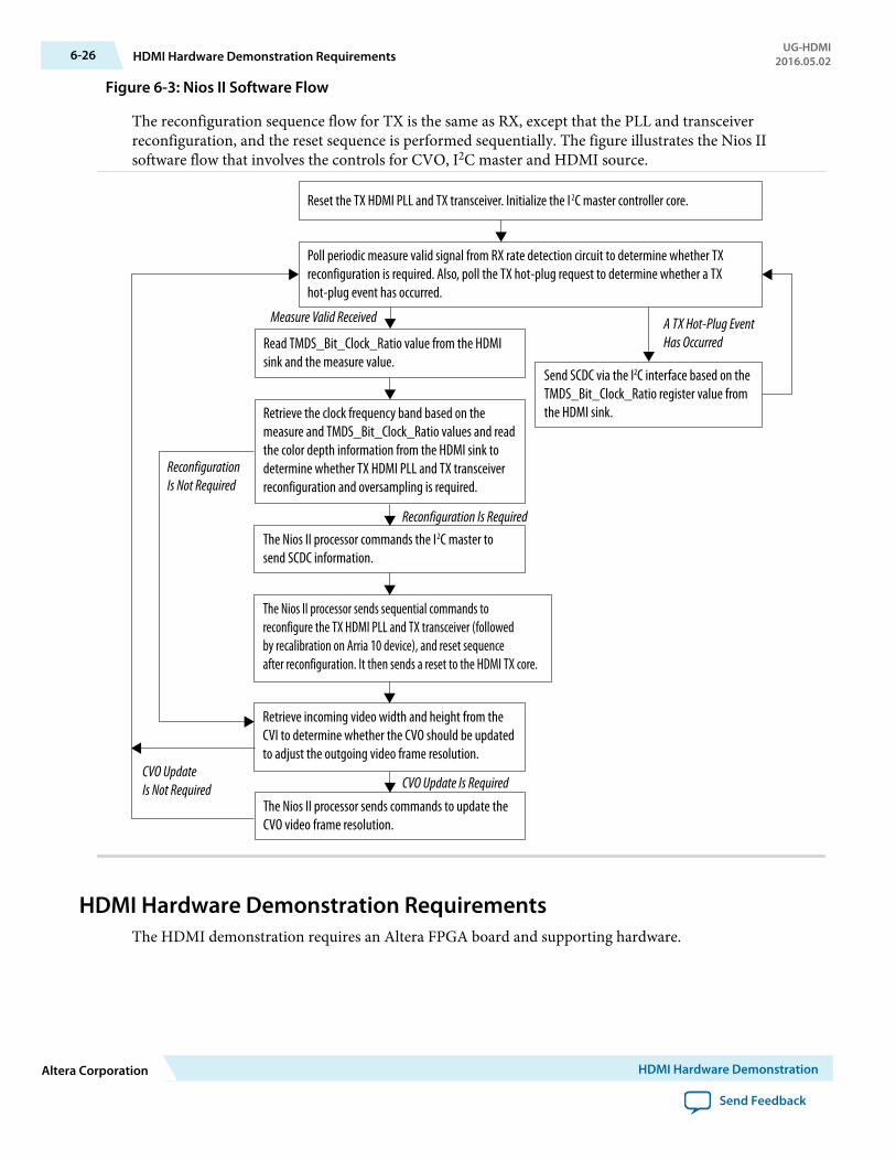
Figure 6-3: Nios II Software Flow
The reconfiguration sequence flow for TX is the same as RX, except that the PLL and transceiverreconfiguration, and the reset sequence is performed sequentially. The figure illustrates the Nios IIsoftware flow that involves the controls for CVO, I2C master and HDMI source.
Reset the TX HDMI PLL and TX transceiver. Initialize the I 2C master controller core.
Poll periodic measure valid signal from RX rate detection circuit to determine whether TX reconfiguration is required. Also, poll the TX hot-plug request to determine whether a TX hot-plug event has occurred.
Read TMDS_Bit_Clock_Ratio value from the HDMI sink and the measure value.
Send SCDC via the I2C interface based on the TMDS_Bit_Clock_Ratio register value from the HDMI sink.Retrieve the clock frequency band based on the
measure and TMDS_Bit_Clock_Ratio values and read the color depth information from the HDMI sink to determine whether TX HDMI PLL and TX transceiver reconfiguration and oversampling is required.
The Nios II processor sends sequential commands to reconfigure the TX HDMI PLL and TX transceiver (followed by recalibration on Arria 10 device), and reset sequence after reconfiguration. It then sends a reset to the HDMI TX core.
The Nios II processor commands the I2C master to send SCDC information.
Retrieve incoming video width and height from the CVI to determine whether the CVO should be updated to adjust the outgoing video frame resolution.
The Nios II processor sends commands to update the CVO video frame resolution.
Reconfiguration Is Required
Reconfiguration Is Not Required
Measure Valid Received A TX Hot-Plug EventHas Occurred
CVO Update Is RequiredCVO Update Is Not Required
HDMI Hardware Demonstration RequirementsThe HDMI demonstration requires an Altera FPGA board and supporting hardware.
6-26 HDMI Hardware Demonstration RequirementsUG-HDMI
2016.05.02
Altera Corporation HDMI Hardware Demonstration
Send Feedback
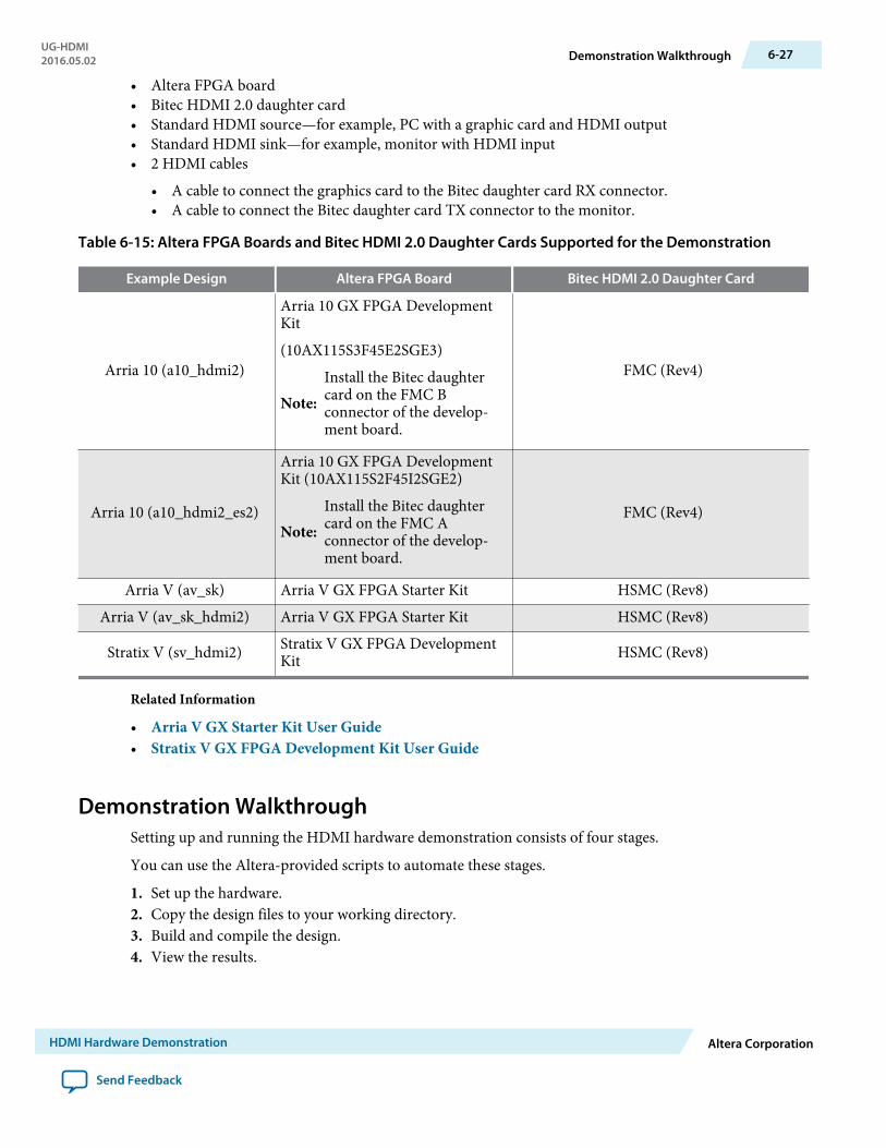
• Altera FPGA board• Bitec HDMI 2.0 daughter card• Standard HDMI source—for example, PC with a graphic card and HDMI output• Standard HDMI sink—for example, monitor with HDMI input• 2 HDMI cables
• A cable to connect the graphics card to the Bitec daughter card RX connector.• A cable to connect the Bitec daughter card TX connector to the monitor.
Table 6-15: Altera FPGA Boards and Bitec HDMI 2.0 Daughter Cards Supported for the Demonstration
Example Design Altera FPGA Board Bitec HDMI 2.0 Daughter Card
Arria 10 (a10_hdmi2)
Arria 10 GX FPGA DevelopmentKit
(10AX115S3F45E2SGE3)
Note:Install the Bitec daughtercard on the FMC Bconnector of the develop‐ment board.
FMC (Rev4)
Arria 10 (a10_hdmi2_es2)
Arria 10 GX FPGA DevelopmentKit (10AX115S2F45I2SGE2)
Note:Install the Bitec daughtercard on the FMC Aconnector of the develop‐ment board.
FMC (Rev4)
Arria V (av_sk) Arria V GX FPGA Starter Kit HSMC (Rev8)Arria V (av_sk_hdmi2) Arria V GX FPGA Starter Kit HSMC (Rev8)
Stratix V (sv_hdmi2) Stratix V GX FPGA DevelopmentKit HSMC (Rev8)
Related Information
• Arria V GX Starter Kit User Guide• Stratix V GX FPGA Development Kit User Guide
Demonstration WalkthroughSetting up and running the HDMI hardware demonstration consists of four stages.
You can use the Altera-provided scripts to automate these stages.
1. Set up the hardware.2. Copy the design files to your working directory.3. Build and compile the design.4. View the results.
UG-HDMI2016.05.02 Demonstration Walkthrough 6-27
HDMI Hardware Demonstration Altera Corporation
Send Feedback
Set Up the HardwareThe first stage of the demonstration is to set up the hardware.
To set up the hardware for the demonstration:
1. Connect the Bitec HDMI 2.0 daughter card to the Altera FPGA board.2. Connect the FPGA board to your PC using a USB cable.
Note: The Arria V GX FPGA Starter Kit and Stratix V GX FPGA Development Kit have an On-BoardUSB-Blaster II connector. If your version of the board does not have this connector, you can usean external USB-Blaster cable.
3. Connect an HDMI cable from the HDMI RX connector on the Bitec HDMI 2.0 daughter card to astandard HDMI source, in this case a PC with a graphic card and HDMI output.
4. Connect another HDMI cable from the HDMI TX connector on the Bitec HDMI 2.0 daughter card toa standard HDMI sink, in this case a monitor with HDMI input.
Copy the Design FilesAfter you set up the hardware, you copy the design files.Copy the hardware demonstration files from one of the following paths to your working directory:
• Arria V
• 2 symbols per clock (HDMI 1.4b) demonstration: <IP root directory>/altera_hdmi/hw_demo/av_sk• 4 symbols per clock (HDMI 2.0) demonstration: <IP root directory>/altera_hdmi/hw_demo/av_sk_
hdmi2• Stratix V
• 2 symbols per clock (HDMI 2.0) demonstration: <IP root directory>/altera_hdmi/hw_demo/sv_hdmi2
• Arria 10 (10AX115S3F45E2SGE3)
• 2 symbols per clock (HDMI 2.0) demonstration: <IP root directory>/altera_hdmi/hw_demo/a10_hdmi2
• Arria 10 (10AX115S2F45I2SGE2)
• 2 symbols per clock (HDMI 2.0) demonstration: <IP root directory>/altera_hdmi/hw_demo/a10_hdmi2_es2
Build and Compile the DesignAfter you copy the design files, you can build the design.
You can use the Altera-provided Tcl script to build and compile the FPGA design.
1. Open a Nios II Command Shell.2. Change the directory to your working directory.3. Type the command and enter.
source runall.tcl (if you are using Quartus Prime Standard Edition) or source runall_pro.tcl(if you are using Quartus Prime Pro Edition)This script executes the following commands:
6-28 Set Up the HardwareUG-HDMI
2016.05.02
Altera Corporation HDMI Hardware Demonstration
Send Feedback

• Generate IP catalog files• Generate the Qsys system• Create a Quartus Prime project• Create a software work space and build the software• Compile the Quartus Prime project• Run Analysis & Synthesis to generate a post-map netlist for DDR assignments—for VIP
passthrough design only• Perform a full compilation
Note: If you are a Linux user, you will get a message cygpath: command not found. You can safelyignore this message; the script will proceed to generate the next commands.
View the ResultsAt the end of the demonstration, you will be able to view the results on the on the standard HDMI sink(monitor).
To view the results of the demonstration, follow these steps:
1. Power up the Altera FPGA board.2. Type the following command on the Nios II Command Shell to download the Software Object File
(.sof) to the FPGA.
nios2-configure-sof output_files/<Quartus project name>.sof3. Power up the standard HDMI source and sink (if you haven't done so).
The design displays the output of your video source (PC).
Note: If the output does not appear, press cpu_resetn to reinitialize the system or perform HPD byunplugging the cable from the standard source and plug it back again.
4. Open the graphic card control utility (if you are using a PC as source). Using the control panel, youcan switch between various video resolutions.The a10_hdmi2, av_hdmi2, and sv_hdmi2 demonstration designs allow any video resolutions up to4Kp60. The av_sk design allows 640×480p60, 720×480p60, 1280×720p60, 1920×1080p60, and3840×2160p24 when you select the VIP passthrough mode (user_dipsw[0] = 0). If you select theVIP bypass mode (user_dipsw[0] = 1, the design allows any video resolutions up to 4Kp60.
Push Buttons, DIP Switches and LEDs FunctionsUse the push buttons, DIP switches, and LED functions on the board to control your demonstration.
Table 6-16: Push Buttons, DIP Switches and LEDs Functions
Push Button/DIP Switch/LED
Pins
Functionsav_sk/av_sk_hdmi2 sv_hdmi2 a10_hdmi2
cpu_resetn D5 AM34 BD27 Press once to perform system reset.
user_pb[0] A14 A7 T12 Press once to toggle HPD signal tothe standard HDMI source.
UG-HDMI2016.05.02 View the Results 6-29
HDMI Hardware Demonstration Altera Corporation
Send Feedback
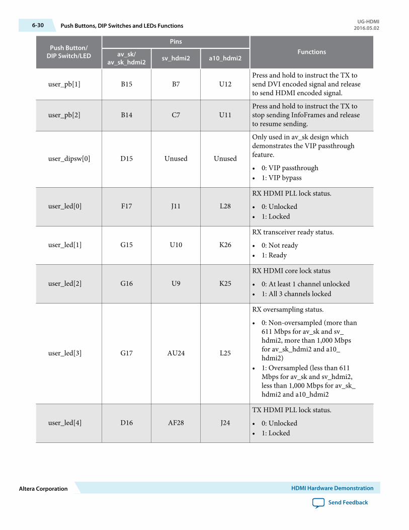
Push Button/DIP Switch/LED
Pins
Functionsav_sk/av_sk_hdmi2 sv_hdmi2 a10_hdmi2
user_pb[1] B15 B7 U12Press and hold to instruct the TX tosend DVI encoded signal and releaseto send HDMI encoded signal.
user_pb[2] B14 C7 U11Press and hold to instruct the TX tostop sending InfoFrames and releaseto resume sending.
user_dipsw[0] D15 Unused Unused
Only used in av_sk design whichdemonstrates the VIP passthroughfeature.
• 0: VIP passthrough• 1: VIP bypass
user_led[0] F17 J11 L28
RX HDMI PLL lock status.
• 0: Unlocked• 1: Locked
user_led[1] G15 U10 K26
RX transceiver ready status.
• 0: Not ready• 1: Ready
user_led[2] G16 U9 K25
RX HDMI core lock status
• 0: At least 1 channel unlocked• 1: All 3 channels locked
user_led[3] G17 AU24 L25
RX oversampling status.
• 0: Non-oversampled (more than611 Mbps for av_sk and sv_hdmi2, more than 1,000 Mbpsfor av_sk_hdmi2 and a10_hdmi2)
• 1: Oversampled (less than 611Mbps for av_sk and sv_hdmi2,less than 1,000 Mbps for av_sk_hdmi2 and a10_hdmi2
user_led[4] D16 AF28 J24
TX HDMI PLL lock status.
• 0: Unlocked• 1: Locked
6-30 Push Buttons, DIP Switches and LEDs FunctionsUG-HDMI
2016.05.02
Altera Corporation HDMI Hardware Demonstration
Send Feedback

Push Button/DIP Switch/LED
Pins
Functionsav_sk/av_sk_hdmi2 sv_hdmi2 a10_hdmi2
user_led[5] C13 AE29 A19
TX transceiver ready status.
• 0: Not ready• 1: Ready
user_led[6] C14 AR7 C18TX transceiver PLL lock status.
• 0: Unlocked• 1: Locked
user_led[7] C16 AV10 D18
TX oversampling status.
• 0: Non-oversampled (more than611 Mbps for av_sk and sv_hdmi2, more than 1,000 Mbpsfor av_sk_hdmi2 and a10_hdmi2)
• 1: Oversampled (less than 611Mbps for av_sk and sv_hdmi2,less than 1,000 Mbps for av_sk_hdmi2 and a10_hdmi2
UG-HDMI2016.05.02 Push Buttons, DIP Switches and LEDs Functions 6-31
HDMI Hardware Demonstration Altera Corporation
Send Feedback
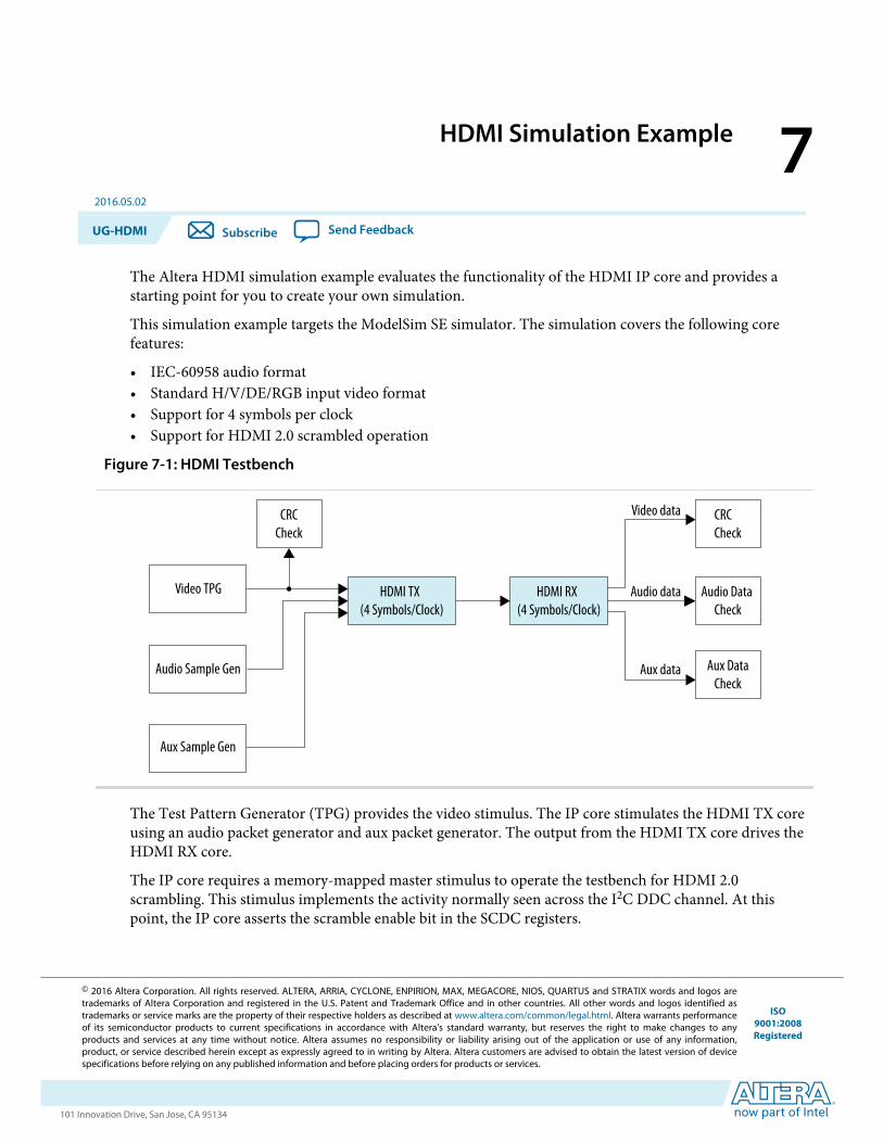
HDMI Simulation Example 72016.05.02
UG-HDMI Subscribe Send Feedback
The Altera HDMI simulation example evaluates the functionality of the HDMI IP core and provides astarting point for you to create your own simulation.
This simulation example targets the ModelSim SE simulator. The simulation covers the following corefeatures:
• IEC-60958 audio format• Standard H/V/DE/RGB input video format• Support for 4 symbols per clock• Support for HDMI 2.0 scrambled operation
Figure 7-1: HDMI Testbench
HDMI TX(4 Symbols/Clock)
HDMI RX(4 Symbols/Clock)
CRCCheck
Video TPG
CRCCheck
Audio data
Video data
Aux data Aux DataCheck
Audio Data Check
Audio Sample Gen
Aux Sample Gen
The Test Pattern Generator (TPG) provides the video stimulus. The IP core stimulates the HDMI TX coreusing an audio packet generator and aux packet generator. The output from the HDMI TX core drives theHDMI RX core.
The IP core requires a memory-mapped master stimulus to operate the testbench for HDMI 2.0scrambling. This stimulus implements the activity normally seen across the I2C DDC channel. At thispoint, the IP core asserts the scramble enable bit in the SCDC registers.
© 2016 Altera Corporation. All rights reserved. ALTERA, ARRIA, CYCLONE, ENPIRION, MAX, MEGACORE, NIOS, QUARTUS and STRATIX words and logos aretrademarks of Altera Corporation and registered in the U.S. Patent and Trademark Office and in other countries. All other words and logos identified astrademarks or service marks are the property of their respective holders as described at www.altera.com/common/legal.html. Altera warrants performanceof its semiconductor products to current specifications in accordance with Altera's standard warranty, but reserves the right to make changes to anyproducts and services at any time without notice. Altera assumes no responsibility or liability arising out of the application or use of any information,product, or service described herein except as expressly agreed to in writing by Altera. Altera customers are advised to obtain the latest version of devicespecifications before relying on any published information and before placing orders for products or services.
ISO9001:2008Registered
www.altera.com101 Innovation Drive, San Jose, CA 95134
The testbench implements CRC checking on the input and output video. The testbench checks the CRCvalue of the transmitted data against the CRC calculated in the received video data. The testbenchperforms the checking after detecting 4 stable V-SYNC signals from the receiver.
The aux sample generator generates a fixed data to be transmitted from the transmitter. On the receiverside, the generator compares whether the expected aux data is received and decoded correctly.
The audio sample generator generates an incrementing test data pattern to be transmitted through theaudio channel. On the receiver side, the audio data checker checks and compares whether theincrementing test data pattern is received and decoded correctly.
Simulation WalkthroughSetting up and running the HDMI simulation example consists of two steps.
1. Copy the simulation files from <IP root directory>/altera/altera_hdmi/sim_example to your workingdirectory.
2. Generate the IP simulation files and scripts, compile, and simulate.a. Open your command prompt.b. Type the command below and enter.
sh runall.sh
This script executes the following commands:
7-2 Simulation WalkthroughUG-HDMI
2016.05.02
Altera Corporation HDMI Simulation Example
Send Feedback
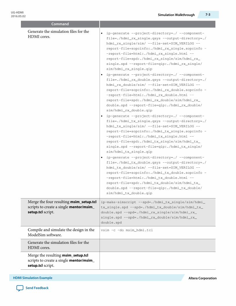
Command
Generate the simulation files for theHDMI cores.
• ip-generate --project-directory=./ --component-
file=./hdmi_rx_single.qsys --output-directory=./
hdmi_rx_single/sim/ --file-set=SIM_VERILOG --
report-file=sopcinfo:./hdmi_rx_single.sopcinfo -
-report-file=html:./hdmi_rx_single.html --
report-file=spd:./hdmi_rx_single/sim/hdmi_rx_
single.spd --report-file=qip:./hdmi_rx_single/
sim/hdmi_rx_single.qip
• ip-generate --project-directory=./ --component-
file=./hdmi_rx_double.qsys --output-directory=./
hdmi_rx_double/sim/ --file-set=SIM_VERILOG --
report-file=sopcinfo:./hdmi_rx_double.sopcinfo -
-report-file=html:./hdmi_rx_double.html --
report-file=spd:./hdmi_rx_double/sim/hdmi_rx_
double.spd --report-file=qip:./hdmi_rx_double/
sim/hdmi_rx_double.qip
• ip-generate --project-directory=./ --component-
file=./hdmi_tx_single.qsys --output-directory=./
hdmi_tx_single/sim/ --file-set=SIM_VERILOG --
report-file=sopcinfo:./hdmi_tx_single.sopcinfo -
-report-file=html:./hdmi_tx_single.html --
report-file=spd:./hdmi_tx_single/sim/hdmi_tx_
single.spd --report-file=qip:./hdmi_tx_single/
sim/hdmi_tx_single.qip
• ip-generate --project-directory=./ --component-
file=./hdmi_tx_double.qsys --output-directory=./
hdmi_tx_double/sim/ --file-set=SIM_VERILOG --
report-file=sopcinfo:./hdmi_tx_double.sopcinfo -
-report-file=html:./hdmi_tx_double.html --
report-file=spd:./hdmi_tx_double/sim/hdmi_tx_
double.spd --report-file=qip:./hdmi_tx_double/
sim/hdmi_tx_double.qip
Merge the four resulting msim_setup.tclscripts to create a single mentor/msim_setup.tcl script.
ip-make-simscript --spd=./hdmi_tx_single/sim/hdmi_
tx_single.spd --spd=./hdmi_tx_double/sim/hdmi_tx_
double.spd --spd=./hdmi_rx_single/sim/hdmi_rx_
single.spd --spd=./hdmi_rx_double/sim/hdmi_rx_
double.spd
Compile and simulate the design in theModelSim software.
vsim -c -do msim_hdmi.tcl
Generate the simulation files for theHDMI cores.
Merge the resulting msim_setup.tclscripts to create a single mentor/msim_setup.tcl script.
UG-HDMI2016.05.02 Simulation Walkthrough 7-3
HDMI Simulation Example Altera Corporation
Send Feedback
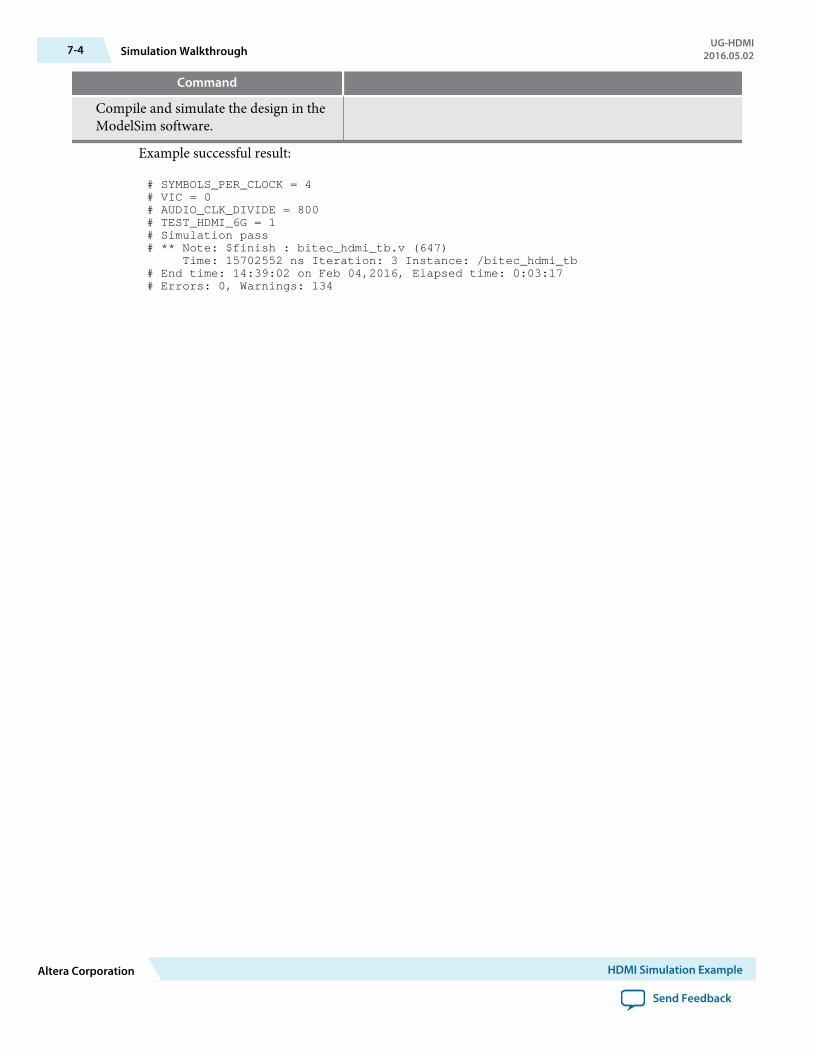
Command
Compile and simulate the design in theModelSim software.
Example successful result:
# SYMBOLS_PER_CLOCK = 4# VIC = 0# AUDIO_CLK_DIVIDE = 800# TEST_HDMI_6G = 1# Simulation pass# ** Note: $finish : bitec_hdmi_tb.v (647) Time: 15702552 ns Iteration: 3 Instance: /bitec_hdmi_tb# End time: 14:39:02 on Feb 04,2016, Elapsed time: 0:03:17# Errors: 0, Warnings: 134
7-4 Simulation WalkthroughUG-HDMI
2016.05.02
Altera Corporation HDMI Simulation Example
Send Feedback

HDMI IP Core User Guide Archives A2016.05.02
UG-HDMI Subscribe Send Feedback
If an IP core version is not listed, the user guide for the previous IP core version applies.IP Core Version User Guide
15.1 HDMI IP Core User Guide
15.0 HDMI IP Core User Guide
14.1 HDMI IP Core User Guide
© 2016 Altera Corporation. All rights reserved. ALTERA, ARRIA, CYCLONE, ENPIRION, MAX, MEGACORE, NIOS, QUARTUS and STRATIX words and logos aretrademarks of Altera Corporation and registered in the U.S. Patent and Trademark Office and in other countries. All other words and logos identified astrademarks or service marks are the property of their respective holders as described at www.altera.com/common/legal.html. Altera warrants performanceof its semiconductor products to current specifications in accordance with Altera's standard warranty, but reserves the right to make changes to anyproducts and services at any time without notice. Altera assumes no responsibility or liability arising out of the application or use of any information,product, or service described herein except as expressly agreed to in writing by Altera. Altera customers are advised to obtain the latest version of devicespecifications before relying on any published information and before placing orders for products or services.
ISO9001:2008Registered
www.altera.com101 Innovation Drive, San Jose, CA 95134
Document Revision History for HDMI UserGuide B
2016.05.02
UG-HDMI Subscribe Send Feedback
Date Version Changes
May 2015 2016.05.02 • Updated the HDMI IP core resource utilization table with 16.0information.
• Added information about Audio Metadata Packet for HDMI Specifi‐cation Version 2.0.
• Added information about new HDMI source ports:
• audio_metadata[164:0]
• audio_format[4:0]
• Added information about new HDMI sink ports:
• audio_metadata[164:0]
• audio_format[4:0]
• vid_lock
• aux_error
• Provided detailed information about the HDMI source and sinkaudio_de[7:0] port.
• Updated the testbench diagram and description to include audio dataand auxiliary data information.
• Added a note for Altera PLL to place the PLL in the transmit path(pll_hdmi_tx) in the physical location next to the transceiver PLL.
• Updated the HDMI sideband signals (HDMI AVI and VSI bit-fields)with default values.
• Added links to archived versions of the HDMI IP Core User Guide.
© 2016 Altera Corporation. All rights reserved. ALTERA, ARRIA, CYCLONE, ENPIRION, MAX, MEGACORE, NIOS, QUARTUS and STRATIX words and logos aretrademarks of Altera Corporation and registered in the U.S. Patent and Trademark Office and in other countries. All other words and logos identified astrademarks or service marks are the property of their respective holders as described at www.altera.com/common/legal.html. Altera warrants performanceof its semiconductor products to current specifications in accordance with Altera's standard warranty, but reserves the right to make changes to anyproducts and services at any time without notice. Altera assumes no responsibility or liability arising out of the application or use of any information,product, or service described herein except as expressly agreed to in writing by Altera. Altera customers are advised to obtain the latest version of devicespecifications before relying on any published information and before placing orders for products or services.
ISO9001:2008Registered
www.altera.com101 Innovation Drive, San Jose, CA 95134
Date Version Changes
November2015
2015.11.02 • Updated the HDMI IP core resource utilization table with 15.1information.
• Changed instances of Quartus II to Quartus Prime.• Added full support for Arria 10 devices.• Added support for new features:
• Deep color• 8-channel audio
• Added the following parameters for HDMI source:
• Support for 8-channel audio• Support for deep color
• Added the following parameters for HDMI sink:
• Support for 8-channel audio• Support for deep color• Manufacturer OUI• Device ID String• Hardware Revision
• Updated the following interface ports for HDMI source:
• Added ctrl port• Removed gcp_Set_AVMute and gcp_Clear_AVMute ports
• Updated the following interface ports for HDMI sink:
• Added ctrl , mode, in_5v_power, and in_hpd ports• Removed gcp_Set_AVMute and gcp_Clear_AVMute ports
• Updated the HDMI sink and source block diagrams to reflect the newfeatures.
• Provided block diagrams for deep color mapping.• Generalized the HDMI hardware demonstration design for all
supported device families (Arria V, Stratix V, and Arria 10) withdetailed description.
B-2 Document Revision History for HDMI User GuideUG-HDMI
2016.05.02
Altera Corporation Document Revision History for HDMI User Guide
Send Feedback
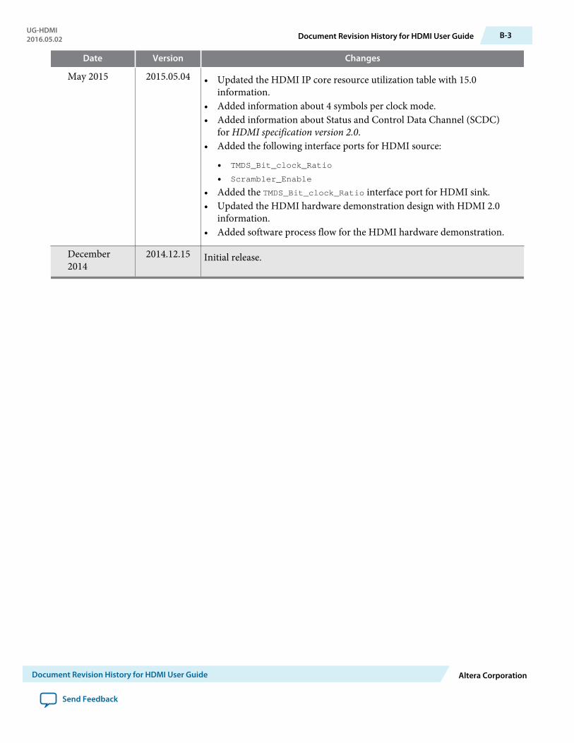
Date Version Changes
May 2015 2015.05.04 • Updated the HDMI IP core resource utilization table with 15.0information.
• Added information about 4 symbols per clock mode.• Added information about Status and Control Data Channel (SCDC)
for HDMI specification version 2.0.• Added the following interface ports for HDMI source:
• TMDS_Bit_clock_Ratio
• Scrambler_Enable
• Added the TMDS_Bit_clock_Ratio interface port for HDMI sink.• Updated the HDMI hardware demonstration design with HDMI 2.0
information.• Added software process flow for the HDMI hardware demonstration.
December2014
2014.12.15 Initial release.
UG-HDMI2016.05.02 Document Revision History for HDMI User Guide B-3
Document Revision History for HDMI User Guide Altera Corporation
Send Feedback