an 119: implementing high-speed search applications with altera cam
TRANSCRIPT
®
Implementing High-SpeedSearch Applications with
Altera CAM
July 2001, ver. 2.1 Application Note 119
Introduction Most memory devices store and retrieve data by addressing specific memory locations. For example, a system using RAM or ROM searches sequentially through memory to locate data. However, this technique can slow system performance since the search requires multiple clock cycles to complete.
You can considerably reduce the time required to find an item stored in memory by identifying stored data by content, rather than by its address. Memory accessed in this way is called content-addressable memory (CAM). CAM offers a performance advantage over other memory search algorithms, such as binary-based searches, tree-based searches, or look-aside tag buffers, because it simultaneously compares the desired information against the entire list of pre-stored entries. Thus, CAM provides an order-of-magnitude reduction in the search time.
CAM is ideally suited for many applications, including Ethernet address look-up, data compression, pattern recognition, cache tags, fast routing table look-up, high-bandwidth address filtering, user privileges, and security and encryption information.
This application note discusses the following topics:
� CAM Fundamentals� CAM in Altera Devices� CAM Applications
CAM Fundamentals
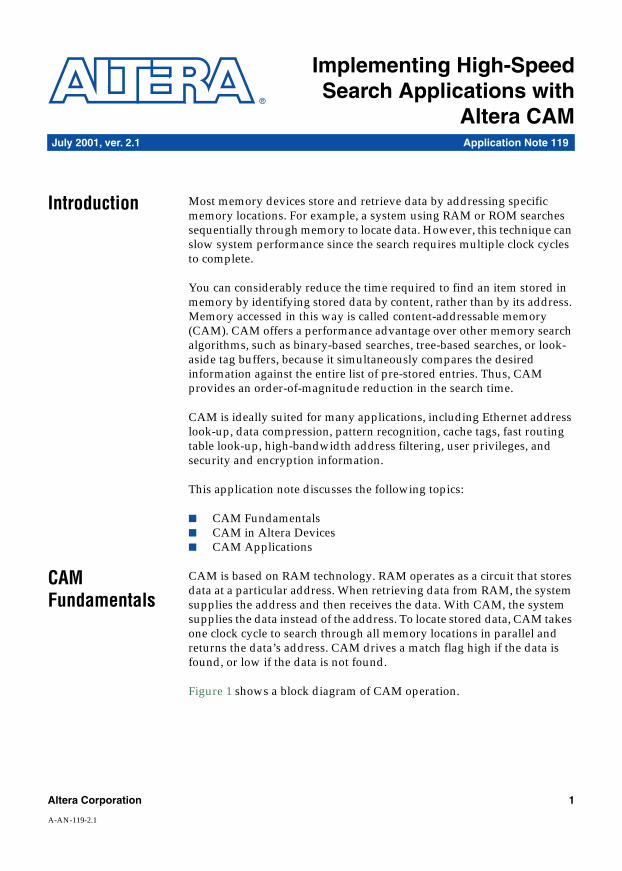
CAM is based on RAM technology. RAM operates as a circuit that stores data at a particular address. When retrieving data from RAM, the system supplies the address and then receives the data. With CAM, the system supplies the data instead of the address. To locate stored data, CAM takes one clock cycle to search through all memory locations in parallel and returns the data’s address. CAM drives a match flag high if the data is found, or low if the data is not found.
Figure 1 shows a block diagram of CAM operation.
Altera Corporation 1
A-AN-119-2.1
AN 119: Implementing High-Speed Search Applications with Altera CAM
2 Altera Corporation
Figure 1. CAM Block Diagram
CAM Accelerates Searches
CAM can accelerate applications requiring fast searches of databases, lists, or patterns, such as in image or voice recognition. For example, the search key could be a network user’s internet protocol (IP) address, and the associated information could be a user’s access privileges and location on the network. If the search key presented is available in CAM, CAM indicates a match and returns the associated information, i.e., the user’s privileges.
CAM Integration
Currently, most applications requiring fast searches use discrete CAM. Designers must add a separate CAM device to their printed circuit board (PCB), which increases design time and reduces the amount of usable PCB space. Discrete CAM also reduces system performance because it introduces additional on-chip and off-chip delays.
APEX 20KE, APEX 20KC, APEX II, and Mercury devices, which contain on-chip CAM built into their embedded system blocks (ESBs), eliminate the disadvantages of discrete CAM. Altera on-chip CAM has an access time of 4 ns, compared to a 20-ns access time for a typical discrete CAM. Because CAM is integrated inside an Altera device, it provides faster system performance than traditional discrete CAM. Altera device CAM is optimized for small- and medium-sized applications that are described in the “CAM Applications” section on page 8. APEX 20KE, APEX 20KC, APEX II, and Mercury devices all offer CAM support as described in this application note
CAM in Altera Devices
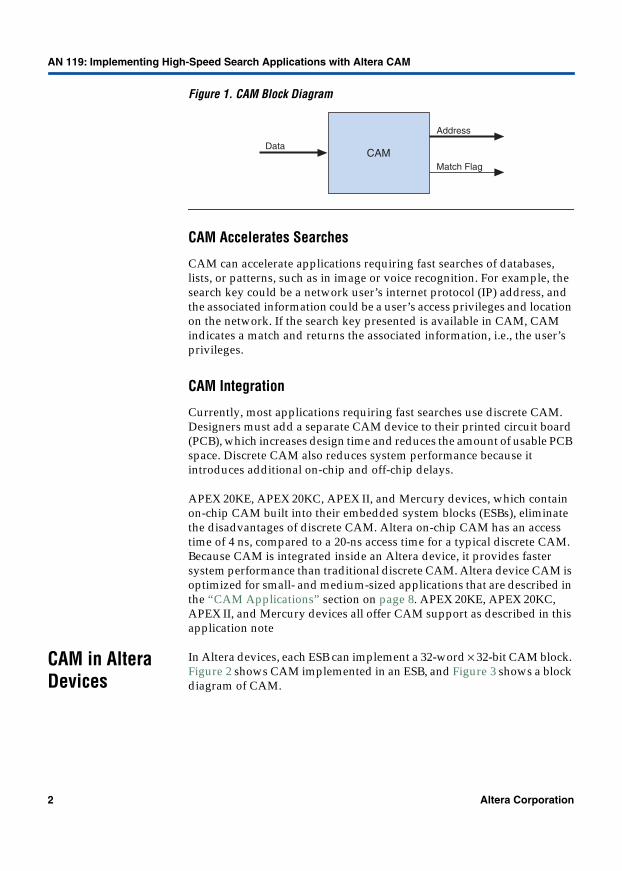
In Altera devices, each ESB can implement a 32-word × 32-bit CAM block. Figure 2 shows CAM implemented in an ESB, and Figure 3 shows a block diagram of CAM.
CAMData
Address
Match Flag
AN 119: Implementing High-Speed Search Applications with Altera CAM
Figure 2. Implementing CAM in an ESB
Figure 3. Altera CAM Block Diagram
Writing to Altera CAM
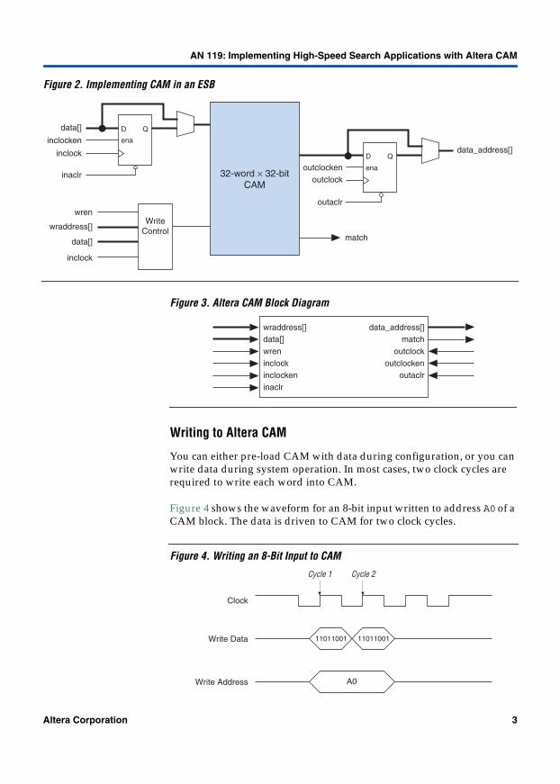
You can either pre-load CAM with data during configuration, or you can write data during system operation. In most cases, two clock cycles are required to write each word into CAM.
Figure 4 shows the waveform for an 8-bit input written to address A0 of a CAM block. The data is driven to CAM for two clock cycles.
Figure 4. Writing an 8-Bit Input to CAM
D
ena
Qdata[]
inclocken
inclock
inclock
inaclr
D
ena
Q
outclockoutclocken
data_in
REwren
wraddress[]
data[]
WriteControl
data_address[]
Comparator32-word × 32-bitCAM
outaclr
match
wraddress[]data[]wreninclockinclockeninaclr
data_address[]match
outclockoutclocken
outaclr
Cycle 1 Cycle 2
Clock
Write Data
Write Address
11011001 11011001
A0
Altera Corporation 3

AN 119: Implementing High-Speed Search Applications with Altera CAM
4 Altera Corporation
A design can write “don’t care” bits into CAM words; bits set to “don’t care” do not affect matching. The “don’t care” bits can be used as a mask for CAM comparisons. A third clock cycle is required when “don’t care” bits are used. The “don’t care” bits are signified by inverting them on the third clock cycle.
Figure 5 shows the waveform for a 1101x100 word (with a “don’t care” bit) written to CAM.
Figure 5. Writing 1101x100 to CAM
Reading from Altera CAM
Altera CAM outputs operate in one of three different modes: single-match mode, multiple-match mode, and fast multiple-match mode. In each mode, an ESB outputs the matched data’s location as an encoded or unencoded address. The address of the matched data is indicated in an encoded output. In an unencoded output, each output represents one word of the CAM block. If an output goes high, then the corresponding address is a match (e.g., if the data is located in address 15, the fifteenth output line goes high).
Single match mode is better suited for designs without duplicate data in the memory. Acquiring outputs in this mode requires only one clock cycle. Figure 6 shows an encoded CAM output.
Cycle 1 Cycle 2 Cycle 3
Clock
Write Data 11010100 11010100 11011100
"Don't Care" Bit

AN 119: Implementing High-Speed Search Applications with Altera CAM
Altera Corporation 5
Figure 6. Encoded CAM Output
If the same data is written into multiple locations in the memory, CAM should be used in multiple-match or fast multiple-match mode. In these modes, CAM supports multiple-match data and ESB outputs the location of the matched data as an encoded or unencoded address.
An ESB can output up to 16 words each clock cycle. In multiple-match mode, it takes two clock cycles to output the 32 words in the CAM block. The 32 words in an ESB are divided into two sets of 16 words, and one set of 16 words is output each clock cycle. In fast multiple-match mode, only the first set of 16 words is output, and the second set of 16 words is ignored. While it only takes one clock cycle to output the data in an ESB, only half of each ESB is used, limiting their capacity to 16 words. Figure 7 shows the CAM’s unencoded output.
Figure 7. Unencoded CAM Output
Notes:(1) For an unencoded output, the ESB only supports 31 input data bits. One input bit
is used by the select line to choose one of the two banks of 16 outputs.(2) If the select input is a 1, then CAM outputs words 0 through 15. If the select
input is a 0, CAM outputs words 16 through 31.
CAM
data[31..0] = 45
addr[4..0] = 02Encoded Output
match = 1
AddressData
00010203
15274585
CAMdata[30..0] (1)
select (2)
q0
UnencodedOutputs
q15
clock
select
unencoded output 0 to 15 16 to 31
AN 119: Implementing High-Speed Search Applications with Altera CAM
6 Altera Corporation
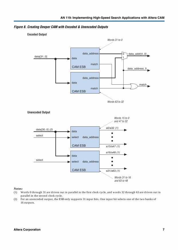
Deeper & Wider CAM Blocks
Each ESB in an Altera device supports a 1-Kbit CAM block (32 words of 32 bits each). You can implement wider or deeper CAM by combining multiple CAM blocks using logic elements (LEs). The QuartusTM II software combines ESBs and LEs automatically to create larger CAM blocks. There is no intrinsic limit to cascading ESBs in an Altera device; all ESBs in a device can be combined into one very large CAM block. For example, by cascading 64 (out of 104) ESBs in an APEX 20KE EP20K400E device, you can generate a 2,048-word × 32-bit or 1,024-word × 64-bit block of CAM. Large Altera devices, such as the EP20K1000E device (with 160 ESBs), can generate a 4,096-word × 32-bit CAM block using 128 ESBs.
Creating Deeper CAM
To create deeper CAM blocks, the Quartus II software cascades the output of each ESB. Both encoded and unencoded CAM outputs are used to create deeper CAM blocks. In an encoded implementation, a multiplexer selects the output of one of the ESBs and drives it out. The select line of the multiplexer is controlled by the match flags of the ESBs. Figure 8 shows an example of a 64-word × 32- or 31-bit CAM block implemented with encoded and unencoded outputs.
AN 119: Implementing High-Speed Search Applications with Altera CAM
Figure 8. Creating Deeper CAM with Encoded & Unencoded Outputs
Notes:(1) Words 0 through 31 are driven out in parallel in the first clock cycle, and words 32 through 63 are driven out in
parallel in the second clock cycle.(2) For an unencoded output, the ESB only supports 31 input bits. One input bit selects one of the two banks of
16 outputs.
CAM ESB
data[31..0]data_addr[4..0]
match
data
data_address
match
CAM ESB
data
data_address
match
data_address_5
Words 31 to 0
Words 63 to 32
Words 15 to 0and 47 to 32
Words 31 to 16and 63 to 48
CAM ESB
data[30..0] (2)
select
select
a0/a32 (1)
a15/a47 (1)
data
select
select data_address
CAM ESB
a16/a48 (1)
a31/a63 (1)
Encoded Output
Unencoded Output
data
data_address
01
Altera Corporation 7

AN 119: Implementing High-Speed Search Applications with Altera CAM
Creating Wider CAM
To increase the width of a CAM block, the Quartus II software cascades the ESB’s unencoded outputs. Encoded outputs cannot be used, because two different data words may coincidentally contain matching portions and cause an incorrect output. To cascade the ESBs, each bit of the first ESB is ANDed with the corresponding bit of the second ESB. When both ESBs report a match, the entire word matches the stored word. Figure 9 shows an example of 32-word × 62-bit CAM implemented with unencoded outputs.
Figure 9. Creating Wider CAM with an Unencoded Output
CAM Applications
CAM is used to accelerate a variety of applications such as local-area networks (LANs), database management, file-storage management, table look up, pattern recognition, artificial intelligence, fully associative and processor-specific cache memories, and disk cache memories. CAM can also perform any search operation.
This section discusses the following applications:
� Data Compression � Network Switch� IP Filters� IP Address Resolution� ATM Switch� Cache Tags� Wireless Basestations� Optimizing CDMA Systems with CAM� Optimizing W-CDMA Systems with CAM� Optimizing a GSM Design with CAM� Cache for Large External CAM� Cache Reference Design
data
select
data_address
CAM ESB
data[30..0]
q0
q15
data
select
data_address
CAM ESB
data[61..31]
q0
q0
q15
q15
select select
8 Altera Corporation

AN 119: Implementing High-Speed Search Applications with Altera CAM
Data Compression
Data compression removes redundancy in a given piece of information, producing an equivalent, but shorter, message. Data compression is particularly useful in communications because devices can transmit the same amount of data using fewer bits.
CAM implements data compression efficiently because it can quickly search through the data structure containing the compression information. Because a good portion of a compression algorithm’s time is spent searching and maintaining this data structure, a hardware search engine can greatly increase the algorithm throughput.
CAM look-up is performed after each word is presented. If the specific code is not found in CAM, another word is shifted in. When the code is found, CAM outputs the appropriate token and the input register is flushed. CAM generates a result in a single transaction regardless of the table size or length of the search list. This process makes CAM ideal for data compression schemes that use sparsely populated tables as part of their algorithm. Figure 10 shows an example of data compression using CAM.
Figure 10. Using CAM for Data Compression
Network Switch
Switch applications use CAM to process the address information from incoming packets. To switch a packet to the correct outgoing port, the incoming packet address is compared with a table of network addresses stored in CAM. CAM outputs the destination for each data packet based on its address.
CAM can store network address and switch port numbers (see Figure 11). CAM in the switch compares gathered data against its stored table. If the comparison yields a match, CAM outputs the destination, and routing control forwards the packet to the correct port.
42 59 83 42 83 27 59
0 1 2 0 2 3 1Compressed Data
Uncompressed DataAddress
0
1
2
3
Data42
59
83
27
CAM Contents
Token
Sequence
Altera Corporation 9

AN 119: Implementing High-Speed Search Applications with Altera CAM
Figure 11. Using CAM as a Network Switch
IP Filters
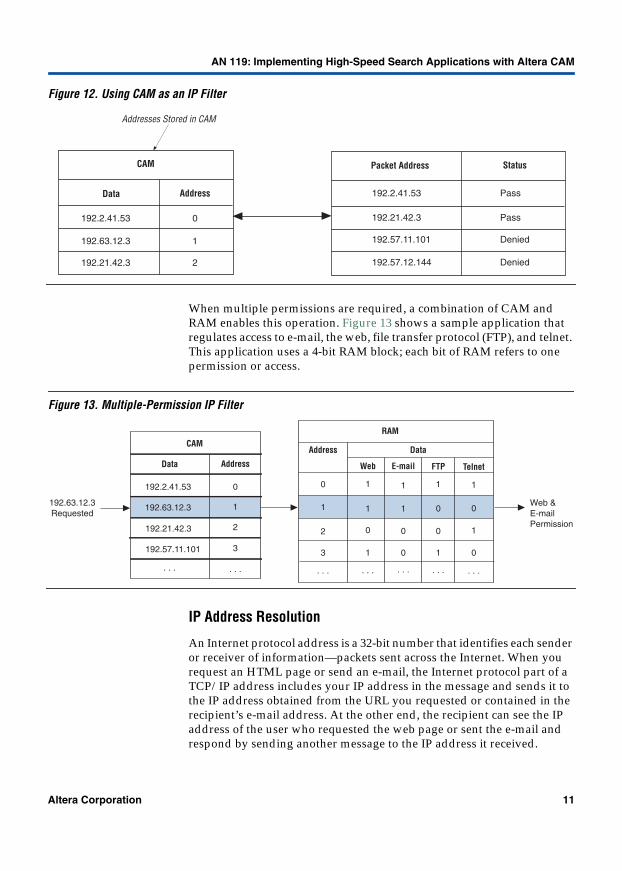
An IP filter is a security feature that prohibits unauthorized users from accessing LAN resources. It can also restrict IP traffic over a wide-area network (WAN) link. With an IP filter, LAN users can be restricted to specific applications on the Internet (such as e-mail). CAM works as a filter to block all access except for packets that have permission. The addresses that have permission are stored in CAM; when an address is sent to memory, CAM reports whether it contains the address. If the address resides within CAM, it has permission for a particular activity. Figure 12 shows an example of an IP filter.
PC2712
PC9743
PC7461
PC6541
PC9811
0
1 2 3
4
Address
0
1
2
3
4
Data
6541
2712
9743
7461
9811
CAM Contents
Switch
Port
NetworkAddress
10 Altera Corporation
AN 119: Implementing High-Speed Search Applications with Altera CAM
Figure 12. Using CAM as an IP Filter
When multiple permissions are required, a combination of CAM and RAM enables this operation. Figure 13 shows a sample application that regulates access to e-mail, the web, file transfer protocol (FTP), and telnet. This application uses a 4-bit RAM block; each bit of RAM refers to one permission or access.
Figure 13. Multiple-Permission IP Filter
IP Address Resolution
An Internet protocol address is a 32-bit number that identifies each sender or receiver of information—packets sent across the Internet. When you request an HTML page or send an e-mail, the Internet protocol part of a TCP/IP address includes your IP address in the message and sends it to the IP address obtained from the URL you requested or contained in the recipient’s e-mail address. At the other end, the recipient can see the IP address of the user who requested the web page or sent the e-mail and respond by sending another message to the IP address it received.
CAM
Data Address
Packet Address Status
192.2.41.53
192.63.12.3
192.21.42.3
0
1
2
192.2.41.53
192.21.42.3
192.57.11.101
192.57.12.144
Pass
Pass
Denied
Denied
Addresses Stored in CAM
RAM
Address Data
Web E-mail FTP Telnet
0
1
2
3
. . .
0
00
0
1 1
1 1
1
1 1
11
0
0
. . . . . . . . . . . .
0
CAM
Data
192.2.41.53
192.63.12.3
192.21.42.3
192.57.11.101
Address
. . . . . .
0
1
2
3
192.63.12.3Requested
Web &E-mailPermission
Altera Corporation 11
AN 119: Implementing High-Speed Search Applications with Altera CAM
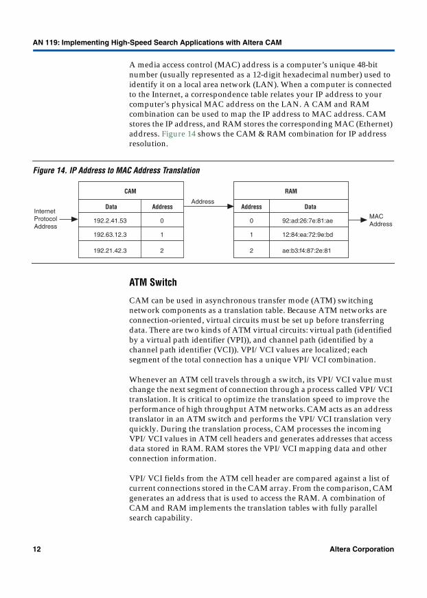
A media access control (MAC) address is a computer’s unique 48-bit number (usually represented as a 12-digit hexadecimal number) used to identify it on a local area network (LAN). When a computer is connected to the Internet, a correspondence table relates your IP address to your computer's physical MAC address on the LAN. A CAM and RAM combination can be used to map the IP address to MAC address. CAM stores the IP address, and RAM stores the corresponding MAC (Ethernet) address. Figure 14 shows the CAM & RAM combination for IP address resolution.
Figure 14. IP Address to MAC Address Translation
ATM Switch
CAM can be used in asynchronous transfer mode (ATM) switching network components as a translation table. Because ATM networks are connection-oriented, virtual circuits must be set up before transferring data. There are two kinds of ATM virtual circuits: virtual path (identified by a virtual path identifier (VPI)), and channel path (identified by a channel path identifier (VCI)). VPI/VCI values are localized; each segment of the total connection has a unique VPI/VCI combination.
Whenever an ATM cell travels through a switch, its VPI/VCI value must change the next segment of connection through a process called VPI/VCI translation. It is critical to optimize the translation speed to improve the performance of high throughput ATM networks. CAM acts as an address translator in an ATM switch and performs the VPI/VCI translation very quickly. During the translation process, CAM processes the incoming VPI/VCI values in ATM cell headers and generates addresses that access data stored in RAM. RAM stores the VPI/VCI mapping data and other connection information.
VPI/VCI fields from the ATM cell header are compared against a list of current connections stored in the CAM array. From the comparison, CAM generates an address that is used to access the RAM. A combination of CAM and RAM implements the translation tables with fully parallel search capability.
CAM
Data Address
RAM
Address Data
192.2.41.53
192.63.12.3
0
1
2192.21.42.3
92:ad:26:7e:81:ae
12:84:ea:72:9e:bd
ae:b3:f4:87:2e:81
InternetProtocolAddress
Address
MAC Address0
1
2
12 Altera Corporation
AN 119: Implementing High-Speed Search Applications with Altera CAM
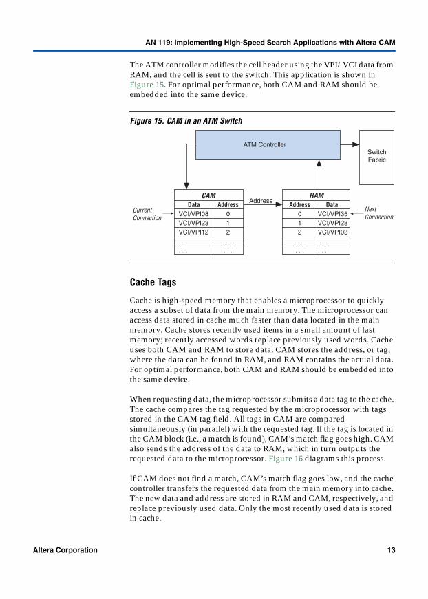
The ATM controller modifies the cell header using the VPI/VCI data from RAM, and the cell is sent to the switch. This application is shown in Figure 15. For optimal performance, both CAM and RAM should be embedded into the same device.
Figure 15. CAM in an ATM Switch
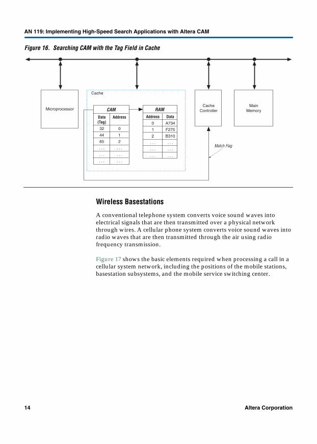
Cache Tags
Cache is high-speed memory that enables a microprocessor to quickly access a subset of data from the main memory. The microprocessor can access data stored in cache much faster than data located in the main memory. Cache stores recently used items in a small amount of fast memory; recently accessed words replace previously used words. Cache uses both CAM and RAM to store data. CAM stores the address, or tag, where the data can be found in RAM, and RAM contains the actual data. For optimal performance, both CAM and RAM should be embedded into the same device.
When requesting data, the microprocessor submits a data tag to the cache. The cache compares the tag requested by the microprocessor with tags stored in the CAM tag field. All tags in CAM are compared simultaneously (in parallel) with the requested tag. If the tag is located in the CAM block (i.e., a match is found), CAM’s match flag goes high. CAM also sends the address of the data to RAM, which in turn outputs the requested data to the microprocessor. Figure 16 diagrams this process.
If CAM does not find a match, CAM’s match flag goes low, and the cache controller transfers the requested data from the main memory into cache. The new data and address are stored in RAM and CAM, respectively, and replace previously used data. Only the most recently used data is stored in cache.
CAM RAMData
VCI/VPI08VCI/VPI23VCI/VPI12. . .. . .
DataVCI/VPI35VCI/VPI28VCI/VPI03. . .. . .
Address012
. . .
. . .
Address012
. . .
. . .
Address
ATM ControllerSwitchFabric
CurrentConnection
NextConnection
Altera Corporation 13
AN 119: Implementing High-Speed Search Applications with Altera CAM
Figure 16. Searching CAM with the Tag Field in Cache
Wireless Basestations
A conventional telephone system converts voice sound waves into electrical signals that are then transmitted over a physical network through wires. A cellular phone system converts voice sound waves into radio waves that are then transmitted through the air using radio frequency transmission.
Figure 17 shows the basic elements required when processing a call in a cellular system network, including the positions of the mobile stations, basestation subsystems, and the mobile service switching center.
Data(Tag)
32
44
65
. . .
. . .
. . .
Address
0
1
2
. . .
. . .
. . .
Data
A734
F275
B310
. . .
. . .
. . .
CAMAddress
0
1
2
. . .
. . .
. . .
RAM
Cache
MicroprocessorMain
MemoryCache
Controller
Match Flag
14 Altera Corporation

AN 119: Implementing High-Speed Search Applications with Altera CAM
Figure 17. General Architecture of a Cellular System Network
The mobile service switching center is the central part of the network subsystem. It switches calls between mobile subscriber units and functions as a switching node for the public telephone network. Other responsibilities include registration, authentication, location updates, handovers, and call routing to roaming subscribers.
Basestation Subsystem
The basestation subsystem (BSS) is composed of two parts: the basestation controller and the transceiver basestation. The basestation controller controls the transceiver basestation and all the control functions and physical links to and from the mobile station. Other responsibilities include handovers, configuration of cell data, control of radio frequency power levels within the transceiver basestation, and supervising the functionality and control of multiple base transceiver units.
The transceiver basestation, which consists of all the radio transmission and reception equipment, handles the radio-link protocols to the mobile station in order to provide coverage to a geographical location.
Mobile Station
The mobile station is the user’s portable device. This device contains mobile equipment.
TransceiverBasestation
TransceiverBasestation
TransceiverBasestation
TransceiverBasestation
Mobile Station
BasestationController
Mobile Service Switching
Center
Public Telephone Network
Base Station Subsystem
Network Subsystem Mobile Station
BasestationController
Equipment Identity Register
Home Identity Register
Authentication Center
Visitor Location Register
Altera Corporation 15

AN 119: Implementing High-Speed Search Applications with Altera CAM
Optimizing CDMA Systems with CAM
Code division multiple access (CDMA) is a form of spread-spectrum transmission where the transmitter spreads the information contained in a particular signal over a much larger bandwidth than the original signal.
A CDMA (IS-95 standard) network consists of a public switching telephone network (PSTN), mobile switching service center, basestation controller, transceiver basestation, and the mobile cell. Each transceiver basestation contains multiple channel elements, and each channel element services one user. Figure 18 shows the CDMA network architecture.
Figure 18. CDMA Network Architecture
The CDMA system uses a 64 × 64-bit Walsh matrix: each Walsh Code is 64-bits long. A Walsh Code is the spreading code, by which the user’s data is spread. Each user is assigned a unique Walsh Code for channelization. The system is responsible for keeping track of which of the 64 Walsh codes is assigned to each channel element. This can be done efficiently by using a combination of CAM and RAM, where CAM provides the Walsh index member for a user, and RAM provides the corresponding 64-bit Walsh Code shown in Figure 19. By using this combination, the system can efficiently track the Walsh Codes used for different users in the system.
Multiplexer
BasestationController
Transceiver Basestation 1
Transceiver Basestation n
Channel Element
Public Switching Telephone
Network
Mobile Service Switching
Center
Mobile Station
Mobile Station
Mobile Station
Mobile Station
Multiplexer
16 Altera Corporation

AN 119: Implementing High-Speed Search Applications with Altera CAM
Figure 19. CAM & RAM Combination to Implement Walsh Code in a CDMA System
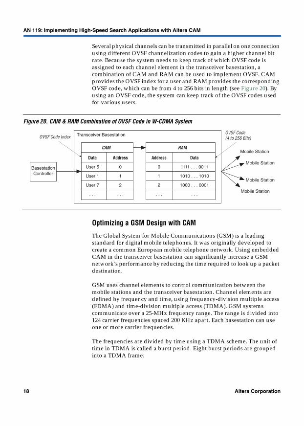
Optimizing W-CDMA Systems with CAM
Wideband code division multiple access (W-CDMA) uses an air interface based on direct sequence CDMA. W-CDMA operates on a wide bandwidth compared to IS-95, in order to meet the IMT 2000 standard. Key features include performance improvement over the second-generation data rate requirement and service flexibility.
Performance Improvement
Using techniques such as power control, variable spreading code, turbo coding, etc., W-CDMA techniques provide higher capacity, lower bit-error rate, and a higher coverage area compared to older-generation technology.
Service Flexibility
W-CDMA has the flexibility to handle mixed services and services with variable bit rates because power is the shared resource between users. In the downlink, the total carrier transmitter power is shared between the users transmitting from the transmission basestation. In the uplink, there is a maximum level of interface power that is shared between the transmitting mobile stations.
The flexibility of W-CDMA is supported by orthogonal variable spreading factor (OVSF) codes for channelization of different users. A user’s data is spread in both the handset and the transceiver basestation using the OVSF codes. OVSF codes maintain downlink transmission orthogonally between users even when they are using different bit rates. One physical resource carries multiple services with different bit rates. As the bit rate changes, the power allocation to the physical resource changes to maintain the quality of service at any instant of connection.
BasestationController
Mobile Station
Mobile Station
Mobile Station
Mobile Station
64-bit Walsh CodeWalsh Code Index
Data
User 5
User 1
User 7
. . .
Address
0
1
2
. . .
Address
0
1
2
. . .
Data
1111 . . . 0011
1010 . . . 1010
1000 . . . 0001
. . .
CAM RAM
Transceiver Basestation
Altera Corporation 17
AN 119: Implementing High-Speed Search Applications with Altera CAM
Several physical channels can be transmitted in parallel on one connection using different OVSF channelization codes to gain a higher channel bit rate. Because the system needs to keep track of which OVSF code is assigned to each channel element in the transceiver basestation, a combination of CAM and RAM can be used to implement OVSF. CAM provides the OVSF index for a user and RAM provides the corresponding OVSF code, which can be from 4 to 256 bits in length (see Figure 20). By using an OVSF code, the system can keep track of the OVSF codes used for various users.
Figure 20. CAM & RAM Combination of OVSF Code in W-CDMA System
Optimizing a GSM Design with CAM
The Global System for Mobile Communications (GSM) is a leading standard for digital mobile telephones. It was originally developed to create a common European mobile telephone network. Using embedded CAM in the transceiver basestation can significantly increase a GSM network’s performance by reducing the time required to look up a packet destination.
GSM uses channel elements to control communication between the mobile stations and the transceiver basestation. Channel elements are defined by frequency and time, using frequency-division multiple access (FDMA) and time-division multiple access (TDMA). GSM systems communicate over a 25-MHz frequency range. The range is divided into 124 carrier frequencies spaced 200 KHz apart. Each basestation can use one or more carrier frequencies.
The frequencies are divided by time using a TDMA scheme. The unit of time in TDMA is called a burst period. Eight burst periods are grouped into a TDMA frame.
BasestationController
Mobile Station
Mobile Station
Mobile Station
Mobile Station
OVSF Code(4 to 256 Bits)OVSF Code Index
Data
User 5
User 1
User 7
. . .
Address
0
1
2
. . .
Address
0
1
2
. . .
Data
1111 . . . 0011
1010 . . . 1010
1000 . . . 0001
. . .
CAM RAM
Transceiver Basestation
18 Altera Corporation

AN 119: Implementing High-Speed Search Applications with Altera CAM
Each mobile station uses a channel, so eight mobile stations or users can gain access to the network on the same TDMA frame. Figure 21 shows how eight users can access a transceiver basestation at one specific frequency.
Figure 21. Eight Channel Elements per Frequency
CAM is used in the transceiver basestation to accelerate the routing of voice and data information. Figure 22 shows how a CAM and RAM combination is used to determine the correct frequency and time slot for a particular mobile station.
Figure 22. CAM & RAM Combination Determine Packet Destination in Transceiver Basestation
Frequency 1
Frequency 2
Frequency 3
Transceiver Basestation
User 1 User 2 User 3 User 4 User 5 User 6 User 7 User 8
User 11 User 10 User 14 User 12 User 20 User 21 User 22 User 24
User 30 User 44 User 19 User 15 User 25 User 26 User 23 User 35
Base Station
Controller
Mobile Station
Mobile Station
Mobile Station
Mobile Station
Data
User 5
User 1
User 7
. . .
Address
0
1
2
. . .
Address
0
1
2
. . .
Data
1111 . . . 0011
1010 . . . 1010
1000 . . . 0001
. . .
CAM RAM
Base Transceiver Station
User 5 User 7
Altera Corporation 19
AN 119: Implementing High-Speed Search Applications with Altera CAM
Using CAM embedded in Altera devices rather than a discrete CAM device speeds the GSM network’s routing process. Embedded CAM eliminates on- and off-chip delays associated with discrete CAM. The embedded CAM device also cuts design time and reduces the board size by eliminating the need for a second device on the board.
A typical transceiver basestation manager calls for up to 128 mobile stations; therefore, a 128-word CAM block is required. A 128-word CAM block can be easily integrated into four ESBs on a single APEX device.
Cache for Large External CAM
Cache speeds memory access by providing an embedded structure that stores words that are commonly requested from the external CAM. Because cache is faster and has less latency than an external device, it can present the requesting system with a match address several clock cycles before the external CAM. Cache is connected in parallel with the external memory source; when the system sends a read request, it will send the data simultaneously to the cache and the external CAM. If the data word is stored in the cache, it will report to the system that it has found a match, which in most cases is several clock cycles before the external CAM will find a match. If the cache reports a miss, it will wait for the external CAM to find a match and the cache will then proceed to write the new word and address.
CAM cache is a combination of CAM and RAM elements. CAM cache cannot be implemented exclusively in CAM because the CAM cache has a smaller address width (five bits) than the external CAM due to the smaller size of the cache. For example, a 32-word cache has an address width of five bits, whereas a 256-word CAM has an address width of eight bits, making it three bits too long for CAM cache. A RAM block is required to store the additional three address bits that the CAM block cannot store. Figure 23 shows a block diagram of the fully associative cache.
20 Altera Corporation

AN 119: Implementing High-Speed Search Applications with Altera CAM
Figure 23. Block Diagram of a Fully Associative Cache
The CAM system is modeled by the block diagram in Figure 24. As the diagram indicates, the cache uses registers on the inputs, which produces a two-cycle hit latency. Any of these registers can be removed to reduce the latency at the expense of the maximum frequency.
Figure 24. CAM Cache Block Diagram
Data(Tag)
45
61
21
1C
Address
00
01
10
11
Address
00
01
10
11
Data
00110
00011
01000
11111
CAM RAM
CacheController
Data
Address Address from external CAM
Data out toExternal CAM
ram_widthadd ex_widthadd
5
2
5
SystemExternal
CAM
Data Data
AddressAddress
APEX 20KE Device
Internal Cache
CAM RAM
Altera Corporation 21

AN 119: Implementing High-Speed Search Applications with Altera CAM
Cache Reference Design
Altera has created reference designs to implement either direct mapped or fully associative cache. These designs are available on the Altera web site (http://www.altera.com). Table 1 describes the input and output ports of the cache reference designs. Table 2 describes the parameters used to customize the cache reference designs.
Table 1. Cache Reference Designs Port Listing
Port Name Required Type Description
clock Yes Input Clock signal for all registers
aclr Yes Input Register clear signal
data_valid Yes Input Indicates the current value on the datain bus is registered and initiates the search process
datain[] Yes Input Input data for searching, writing, or erasing from cache
write Yes Input Indicates that cache should write the values on the address_ext and datain buses
delete Yes Input Deletes the values on the datain and address_ext buses from cache
ext_match_found Yes Input Indicates that external CAM has found a match; address_ext reflects the matching address when ext_match_found is high
address_ext[] Yes Input Address or associated data value from the external process
cache_busy No Output Indicates that cache is busy writing or erasing
cache_hit Yes Output Signals that cache has found a match for data at the address indicated by cache_address
dataout[] Yes Output Contains the associated data for the value on the datain bus
22 Altera Corporation
AN 119: Implementing High-Speed Search Applications with Altera CAM
Quartus II Software Support
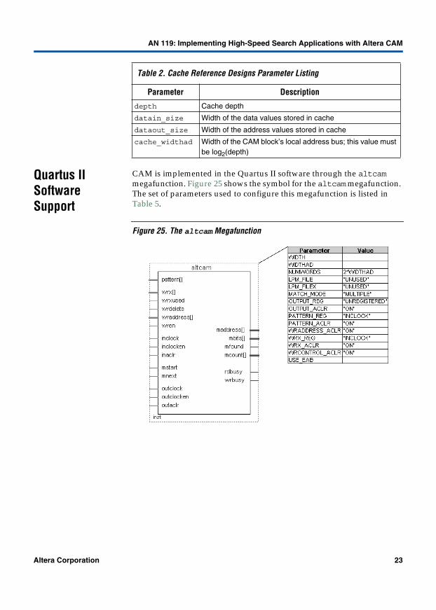
CAM is implemented in the Quartus II software through the altcam megafunction. Figure 25 shows the symbol for the altcam megafunction. The set of parameters used to configure this megafunction is listed in Table 5.
Figure 25. The altcam Megafunction
Table 2. Cache Reference Designs Parameter Listing
Parameter Description
depth Cache depth
datain_size Width of the data values stored in cache
dataout_size Width of the address values stored in cache
cache_widthad Width of the CAM block’s local address bus; this value must be log2(depth)
Altera Corporation 23
AN 119: Implementing High-Speed Search Applications with Altera CAM
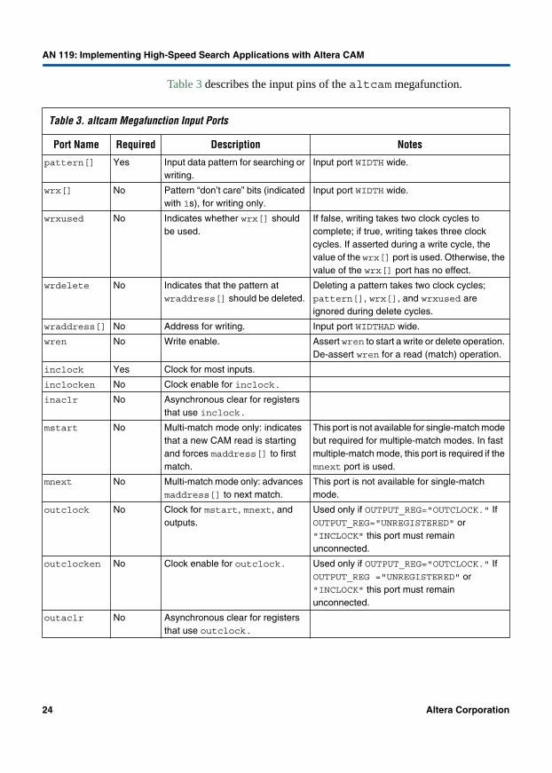
Table 3 describes the input pins of the altcam megafunction.
Table 3. altcam Megafunction Input Ports
Port Name Required Description Notes
pattern[] Yes Input data pattern for searching or writing.
Input port WIDTH wide.
wrx[] No Pattern “don’t care” bits (indicated with 1s), for writing only.
Input port WIDTH wide.
wrxused No Indicates whether wrx[] should be used.
If false, writing takes two clock cycles to complete; if true, writing takes three clock cycles. If asserted during a write cycle, the value of the wrx[] port is used. Otherwise, the value of the wrx[] port has no effect.
wrdelete No Indicates that the pattern at wraddress[] should be deleted.
Deleting a pattern takes two clock cycles; pattern[], wrx[], and wrxused are ignored during delete cycles.
wraddress[] No Address for writing. Input port WIDTHAD wide.
wren No Write enable. Assert wren to start a write or delete operation. De-assert wren for a read (match) operation.
inclock Yes Clock for most inputs.
inclocken No Clock enable for inclock.
inaclr No Asynchronous clear for registers that use inclock.
mstart No Multi-match mode only: indicates that a new CAM read is starting and forces maddress[] to first match.
This port is not available for single-match mode but required for multiple-match modes. In fast multiple-match mode, this port is required if the mnext port is used.
mnext No Multi-match mode only: advances maddress[] to next match.
This port is not available for single-match mode.
outclock No Clock for mstart, mnext, and outputs.
Used only if OUTPUT_REG="OUTCLOCK." If OUTPUT_REG="UNREGISTERED" or "INCLOCK" this port must remain unconnected.
outclocken No Clock enable for outclock. Used only if OUTPUT_REG="OUTCLOCK." If OUTPUT_REG ="UNREGISTERED" or "INCLOCK" this port must remain unconnected.
outaclr No Asynchronous clear for registers that use outclock.
24 Altera Corporation

AN 119: Implementing High-Speed Search Applications with Altera CAM
Table 4 describes the output pins of the altcam megafunction.
Table 5 list the parameters that are used to configure the altcam megafunction.
Table 4. altcam Megafunction Output Ports
Port Required Description Comments
maddress[] No Encoded address of current match.
Output port WIDTHAD wide. One of the output ports must be used. Altera recommends using either a combination of the maddress[] and mfound output ports, or the mbits[] output port.
mbits[] No Address of the found match. Output port with width [NUMWORDS-1..0]. One of the output ports must be present. Altera recommends using either a combination of the maddress[] and mfound output ports, or the mbits[] output port.
mfound No Indicates at least one match. Used with the maddress[] port. One of the output ports must be present. Altera recommends using either a combination of the maddress[] and mfound output ports, or the mbits[] output port.
mcount[] No Total number of matches. Output port WIDTHAD wide. One of the output ports must be present. Altera recommends using either a combination of the maddress[] and mfound output ports, or the mbits[] output port.
rdbusy No Indicates that read input ports must hold their current value.
One of the output ports must be present.
wrbusy No Indicates that write input ports must hold their current value.
One of the output ports must be present.
Table 5. altcam Megafunction Parameters (Part 1 of 2)
Parameter Type Required Description
WIDTH Integer Yes Width of the input pattern and stored patterns.
WIDTHAD Integer Yes Width of wraddress[] port. WIDTHAD should be equal to CEIL [LOG2(NUMWORDS)].
NUMWORDS Integer Yes Number of words stored in memory. It indicates the width of the mbits[] port. In general, mbits[] value should be2^ (WIDTHAD-1) < NUMWORDS <= 2^ WIDTHAD.
Altera Corporation 25

AN 119: Implementing High-Speed Search Applications with Altera CAM
Writing Patterns into CAM
Writing a new pattern in altcam or replacing its stored patterns with new patterns involves the use of the pattern[], wrx[], wrxused, wrdelete, wren, and wraddress[] ports. Patterns without “don’t care” bits can be written in two clock cycles, and those with “don’t care” bits require three clock cycles. During all write cycles, wren must be asserted and wraddress[] and pattern[] must remain unchanged.
LPM_FILE String No Name of the Memory Initialization File (.mif) or Hexadecimal (Intel-format) File (.hex) containing RAM initialization data (<file name>), or UNUSED. If omitted, contents default to "never match."
LPM_FILEX String No Name of the second HEX File containing RAM initialization data (<filename>_xu.hex). If omitted the default is UNUSED. Bits that are 1 in this file change the meaning of the bits in the first HEX File such that the 0 bits in the first file become “don't care” bits, and the 1 bits become "never match" bits in CAM patterns. The 0 bits in this file preserve the normal meaning of the bits in the first HEX File.
MATCH_MODE String Yes Selects between single-match mode and one of two multiple-match modes. The values are SINGLE, MULTIPLE, and FAST_MULTIPLE. If omitted, the default is MULTIPLE.
OUTPUT_REG String No Indicates whether the outputs should be registered. Values are UNREGISTERED, INCLOCK, and OUTCLOCK. If omitted, the default is UNREGISTERED.
OUTPUT_ACLR String No Indicates whether the outaclr port should affect the output registers. Values are ON and OFF. If omitted, the default is ON.
PATTERN_REG String No Indicates whether pattern[] should be registered. Values are UNREGISTERED and INCLOCK. If omitted, the default is INCLOCK.
PATTERN_ACLR String No Indicates whether the inaclr port should affect the pattern[] registers. Values are ON and OFF. If omitted, the default is ON.
WRADDRESS_ACLR String No Indicates whether the inaclr port should affect the wraddress[] registers. Values are ON and OFF. If omitted, the default is ON.
WRX_REG String No Indicates whether the wrx[] and wrxused ports should be registered. Values are UNREGISTERED, and INCLOCK. If omitted, the default is INCLOCK.
WRX_ACLR String No Indicates whether the inaclr port affects the wrx[] and wrxused registers. Values are ON and OFF. If omitted, the default is ON.
WRCONTROL_ACLR String No Indicates whether the inaclr port affects the wren register. Values are ON and OFF. If omitted, the default is ON.
Table 5. altcam Megafunction Parameters (Part 2 of 2)
Parameter Type Required Description
26 Altera Corporation
AN 119: Implementing High-Speed Search Applications with Altera CAM
1 The design requires a different hold time if the pattern[] input is unregistered. If unregistered, pattern[] data must be available to the CAM for two complete clock cycles, and not just the rising edge of the clock. By default, pattern[] is registered in the MegaWizard Plug-In Manager.
If the pattern does not contain “don’t care” bits, then asserting pattern[], wren, and wraddress[] for two clock cycles is sufficient. “Don’t care” bits can be added by using the wrx[] port. Bits with 0 in wrx[] mark valid pattern bits, and bits with 1 in wrx[] mark “don’t care” pattern bits. When the wrx[] port is used, the wrx[], wrxused, pattern[], wren, and wraddress[] must be asserted for three clock cycles.
CAM entries can also be deleted by asserting wrdelete and wren for two clock cycles, during which wraddress[] should indicate the address containing the data that is to be deleted. The pattern[], wrx[], and wrxused inputs are ignored during delete cycles.
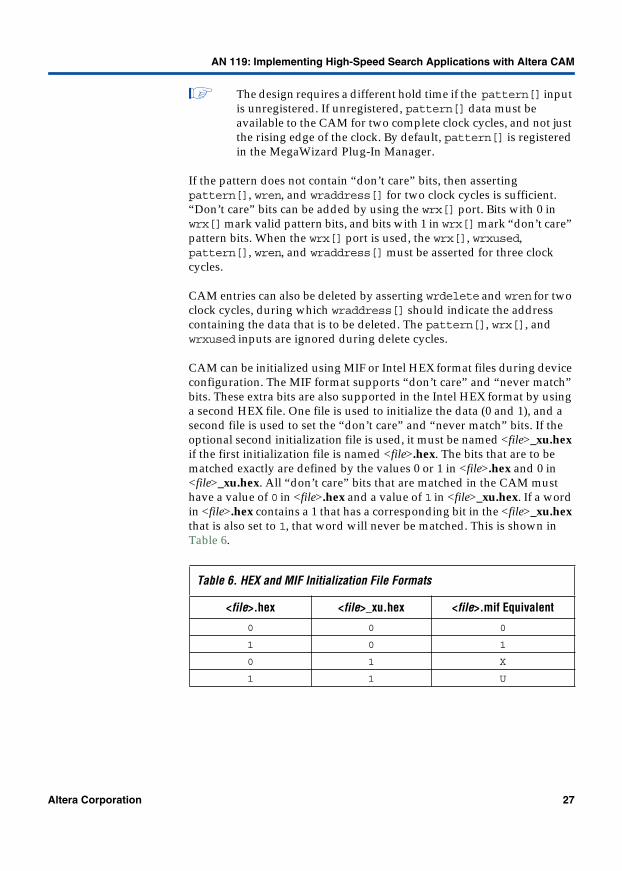
CAM can be initialized using MIF or Intel HEX format files during device configuration. The MIF format supports “don’t care” and “never match” bits. These extra bits are also supported in the Intel HEX format by using a second HEX file. One file is used to initialize the data (0 and 1), and a second file is used to set the “don’t care” and “never match” bits. If the optional second initialization file is used, it must be named <file>_xu.hex if the first initialization file is named <file>.hex. The bits that are to be matched exactly are defined by the values 0 or 1 in <file>.hex and 0 in <file>_xu.hex. All “don’t care” bits that are matched in the CAM must have a value of 0 in <file>.hex and a value of 1 in <file>_xu.hex. If a word in <file>.hex contains a 1 that has a corresponding bit in the <file>_xu.hex that is also set to 1, that word will never be matched. This is shown in Table 6.
Table 6. HEX and MIF Initialization File Formats
<file>.hex <file>_xu.hex <file>.mif Equivalent
0 0 0
1 0 1
0 1 X
1 1 U
Altera Corporation 27
AN 119: Implementing High-Speed Search Applications with Altera CAM
Reading from CAM
To read patterns/addresses from altcam, three different modes can be used:
� Single-match mode� Multiple-match mode � Fast multiple-match mode
In multiple-match and fast multiple-match modes, an external priority encoder generates the encoded match address output maddress[]. As a result, when reading patterns in either of the multiple-match modes, the encoding logic will generally result in higher logic utilization than with single-match mode.
In all three modes, both encoded (maddress[]) and unencoded (mbits[]) outputs are available. External logic generates the mfound and mcount[] signals, which give the total number of matches.
Single-Match Mode
In single-match mode (MATCH_MODE = "SINGLE"), only one inclock clock cycle is needed to read stored data from altcam.
When an input pattern matches one of the stored patterns in altcam, match flag mfound will be asserted, and the address of the match will be presented on maddress[]. Output port mbits[] gives the unencoded version of the match. The output that indicates the number of matches (mcount[]) is always either the value 0 or 1 in this mode.
1 In the single-match mode, altcam will not operate properly if there are multiple patterns stored that match the same input pattern. If this situation occurs, the Quartus II software will give a warning during simulation indicating that CAM contains multiple matches.
In single-match mode, the altcam megafunction will support CAMs deeper than 32 words by using multiple embedded system blocks (ESBs). For input patterns with widths greater than 32 bits, altcam will automatically switch to fast multiple-match mode.
28 Altera Corporation
AN 119: Implementing High-Speed Search Applications with Altera CAM
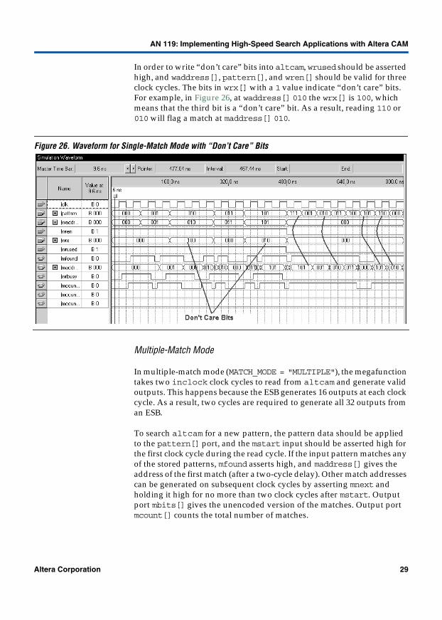
In order to write “don’t care” bits into altcam, wrused should be asserted high, and waddress[], pattern[], and wren[] should be valid for three clock cycles. The bits in wrx[] with a 1 value indicate “don’t care” bits. For example, in Figure 26, at waddress[] 010 the wrx[] is 100, which means that the third bit is a “don’t care” bit. As a result, reading 110 or 010 will flag a match at maddress[] 010.
Figure 26. Waveform for Single-Match Mode with “Don’t Care” Bits
Multiple-Match Mode
In multiple-match mode (MATCH_MODE = "MULTIPLE"), the megafunction takes two inclock clock cycles to read from altcam and generate valid outputs. This happens because the ESB generates 16 outputs at each clock cycle. As a result, two cycles are required to generate all 32 outputs from an ESB.
To search altcam for a new pattern, the pattern data should be applied to the pattern[] port, and the mstart input should be asserted high for the first clock cycle during the read cycle. If the input pattern matches any of the stored patterns, mfound asserts high, and maddress[] gives the address of the first match (after a two-cycle delay). Other match addresses can be generated on subsequent clock cycles by asserting mnext and holding it high for no more than two clock cycles after mstart. Output port mbits[] gives the unencoded version of the matches. Output port mcount[] counts the total number of matches.
Altera Corporation 29

AN 119: Implementing High-Speed Search Applications with Altera CAM
In this mode, each ESB supports 31 bits of data because the most significant bit (MSB) is used to select between the even or odd outputs of ESB at each clock cycle. But multiple-match mode supports both deeper and wider CAMs by cascading 32-word × 31-bit ESBs.
Figure 27 shows the functional simulation waveform for multiple-match mode. In multiple-match mode, the mstart provides the lowest match address location, and mnext provides the consequent match locations on maddress[]. Signal mnext should be asserted not more than two clock cycles after mstart is asserted. In this example, data 1 has been written in two locations: 6 and 10. Asserting mstart provides address location 6 on the maddress[] port, and asserting mnext enables CAM to read out the consequent location, 10.
Figure 27. Waveform for Multiple-Match Mode
Fast Multiple-Match Mode
Fast multiple-match mode (MATCH_MODE = "FAST_MULTIPLE") is identical to multiple-match mode except that fast multiple-match mode only takes one inclock clock cycle to read from altcam and generate valid outputs. However, this quick generation uses only half of the memory available in each ESB. As a result, ESB utilization is higher, but data can be read out of altcam in one cycle.
30 Altera Corporation
AN 119: Implementing High-Speed Search Applications with Altera CAM
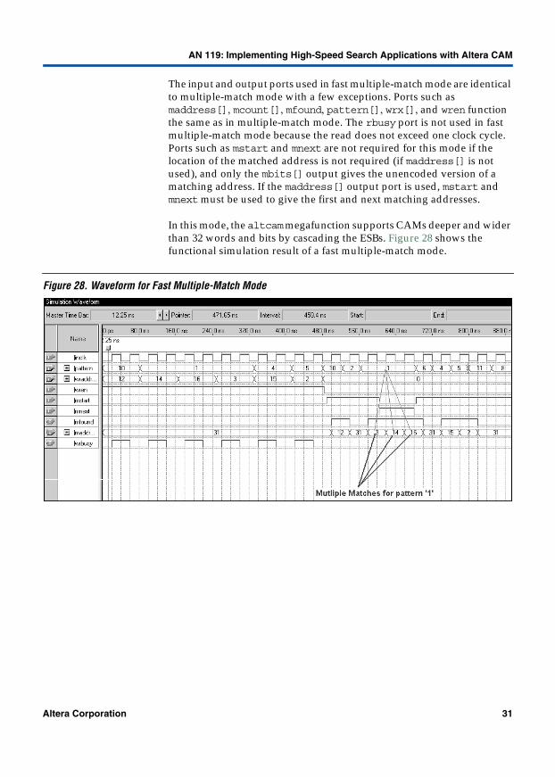
The input and output ports used in fast multiple-match mode are identical to multiple-match mode with a few exceptions. Ports such as maddress[], mcount[], mfound, pattern[], wrx[], and wren function the same as in multiple-match mode. The rbusy port is not used in fast multiple-match mode because the read does not exceed one clock cycle. Ports such as mstart and mnext are not required for this mode if the location of the matched address is not required (if maddress[] is not used), and only the mbits[] output gives the unencoded version of a matching address. If the maddress[] output port is used, mstart and mnext must be used to give the first and next matching addresses.
In this mode, the altcam megafunction supports CAMs deeper and wider than 32 words and bits by cascading the ESBs. Figure 28 shows the functional simulation result of a fast multiple-match mode.
Figure 28. Waveform for Fast Multiple-Match Mode
Altera Corporation 31
AN 119: Implementing High-Speed Search Applications with Altera CAM
CAM Mode Comparison
In order to compare the performance and utilization of the different CAM modes, a 32-word × 32-bit CAM was compiled for an EP20K200E-1 device. Table 7 shows the results of this comparison.
Resource Usage
One ESB can implement a 32-word × 32-bit CAM. Table 8 shows the resource usage for the altcam megafunction.
MegaWizard Interface
The MegaWizardTM Plug-In Manager allows users to specify options for the custom megafunction variations. The MegaWizard Plug-In Manager asks questions about the preferred values for parameters or optional ports.
The MegaWizard Plug-In Manager automatically generates a Component Declaration File (.cmp) that can be used in VHDL Design Files (.vhd), and an Include File (.inc) that can be used in Text Design Files (.tdf) and Verilog Design Files (.v).
Users can start the MegaWizard Plug-In Manager in one of the following ways:
� Choose the MegaWizard Plug-In Manager command (Tools menu).� When working in the Block Editor, click MegaWizard Plug-In
Manager in the Symbol dialog box (Insert menu).
Table 7. CAM Mode Comparison (32 × 32)
Feature Single-Match Mode Multiple-Match Mode Fast Multiple-Match Mode
ESBs used 1 1 2
LEs used 35.0 98 79
fMAX 198.89 (MHz) 94.45 (MHz) 190.91 (MHz)
Table 8. Resource Usage for the altcam Megafunction (32 × 32)
Match Mode CAM Patterns per ESB CAM Pattern Bits per ESB
Single-match mode 32 32
Multiple-match mode 32 31
Fast multiple-match mode 16 32
32 Altera Corporation

AN 119: Implementing High-Speed Search Applications with Altera CAM
Figure 29 shows page 1 of the altcam MegaWizard Plug-In Manager.
Figure 29. Page 1 of altcam MegaWizard Plug-In Manager
Data Input Bus Width
This option allows users to select the width of the input pattern[] of the designed altcam. The pull-down menu shows the value, which goes up to 256 bits. For widths higher than 256 bits, the value must be typed in.
Depth of CAM
This option specifies the number of word lines to the altcam megafunction. Two options are available: entering the number by its entries (word lines) or by the width of address bits.
Operation Mode of CAM
There are three options for altcam operation mode.
� Single match mode: Read occurs in one clock cycle, but it does not support multiple match.
� Multiple match mode: Read occurs in two-clock cycles and supports multiple matches.
� Fast multiple match mode: Read occurs in one clock cycle and supports multiple matches, but it only uses half of an ESB.
Altera Corporation 33
AN 119: Implementing High-Speed Search Applications with Altera CAM
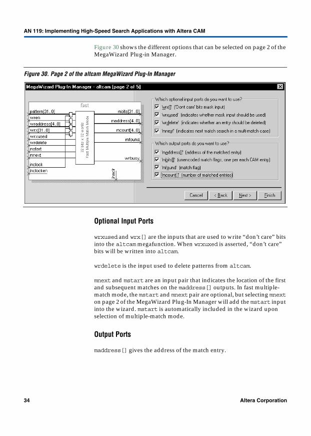
Figure 30 shows the different options that can be selected on page 2 of the MegaWizard Plug-in Manager.
Figure 30. Page 2 of the altcam MegaWizard Plug-In Manager
Optional Input Ports
wrxused and wrx[] are the inputs that are used to write “don’t care” bits into the altcam megafunction. When wrxuxed is asserted, “don’t care” bits will be written into altcam.
wrdelete is the input used to delete patterns from altcam.
mnext and mstart are an input pair that indicates the location of the first and subsequent matches on the maddress[] outputs. In fast multiple-match mode, the mstart and mnext pair are optional, but selecting mnext on page 2 of the MegaWizard Plug-In Manager will add the mstart input into the wizard. mstart is automatically included in the wizard upon selection of multiple-match mode.
Output Ports
maddress[] gives the address of the match entry.
34 Altera Corporation
AN 119: Implementing High-Speed Search Applications with Altera CAM
mbits[] gives the unencoded version of the match location. In multiple-match mode or in fast multiple-match mode, only selecting mbits[] (instead of maddress[]) will reduce the logic cell utilization because the external logic used to encode the unencoded outputs will not be implemented.
When in multiple-match mode or fast multiple-match mode, mcount[] gives the total number of matches found in altcam. In single-match mode, mcount[] only has a value of 0 or 1 because multiple match is not supported in this mode.
mfound is the output that indicates whether any match was found.
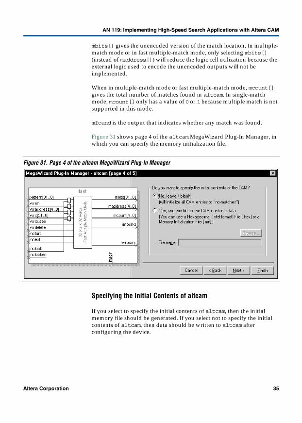
Figure 31 shows page 4 of the altcam MegaWizard Plug-In Manager, in which you can specify the memory initialization file.
Figure 31. Page 4 of the altcam MegaWizard Plug-In Manager
Specifying the Initial Contents of altcam
If you select to specify the initial contents of altcam, then the initial memory file should be generated. If you select not to specify the initial contents of altcam, then data should be written to altcam after configuring the device.
Altera Corporation 35
AN 119: Implementing High-Speed Search Applications with Altera CAM
Two types of memory files exist: MIF and HEX files.
� MIFs specify the pre-loaded pattern in the altcam. Only one file is needed to load patterns incorporating 1, 0, X (“don’t care” bits) and U (“never match” bits). This is an Altera file format and can only be used for CAM functions that are implemented in the Quartus II software. MIFs are not compatible with external simulators.
� HEX files require two files to be created:<file_name>.hex for 1 and 0 patterns<file_name>_ux.hex for U and X
HEX files allow users to use the CAM function in third-party behavioral simulation.
Examples
Figure 32 shows an altcam MegaWizard instantiation in single-match mode. In this example, “don’t care” bits will be written into the altcam through “don’t care” ports. Also, the outputs have been registered.
36 Altera Corporation

AN 119: Implementing High-Speed Search Applications with Altera CAM
Figure 32. altcam Megafunction in Single-Match Mode with “Don’t Care” Ports
Figure 33 shows the instantiation of fast multiple-match mode. In this example, only 1 and 0 will be written into altcam.
pattern[31..0]
wren
wraddress[4..0]
32 bits × 32 words
wrx[31..0]
wrxused
mbits[31..0]
maddress[4..0]
mcount[4..0]
mfound
wrbusy
inclk
inclken
inaclr
Single-Match Mode
Altera Corporation 37

AN 119: Implementing High-Speed Search Applications with Altera CAM
Figure 33. altcam Megafunction in Fast Multiple-Match Mode
When selecting multiple-match mode in the altcam MegaWizard Plug-In Manager (Figure 34), the mstart input will be automatically selected as one of input ports. The user has the option of selecting mnext as an input if detecting the address of all matches is required.
pattern[31..0]
wren
wraddress[4..0]
31 bits × 32 words
mstart
mnext
mbits[31..0]
maddress[4..0]
mcount[4..0]
rdbusy
wrbusy
inclk
inclken
inaclr
Multiple-Match Mode
mfound
38 Altera Corporation

AN 119: Implementing High-Speed Search Applications with Altera CAM
Figure 34. altcam Megafunction in Multiple-Match Mode
VHDL Instantiation
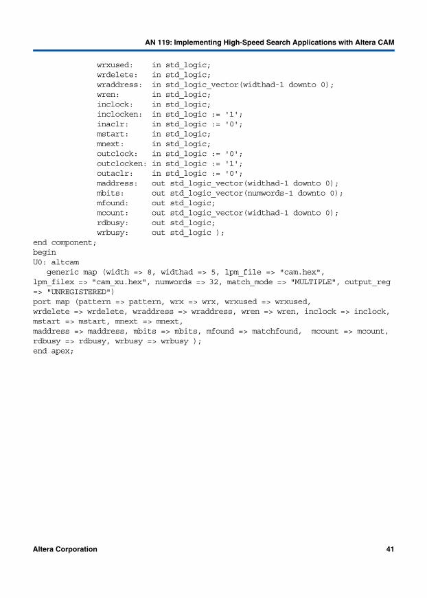
The following example code instantiates the altcam.vhd behavioral model for the altcam megafunction. This particular example instantiates the function, passes parameters, and connects the ports of the altcam to input and output pins to demonstrate the functionality of the CAM. The altcam function can be directly instantiated as shown here along with other RTL code for simulation. This example uses files called cam.hex and cam_xu.hex to initialize the contents. Both files are shown at the end of this document.
pattern[31..0]
wren
wraddress[4..0]
32 bits × 32 words
mstart
mnext
mbits[31..0]
maddress[4..0]
mcount[4..0]
rdbusy
wrbusy
inclk
inclken
inaclr
Multiple-Match Mode
mfound
Altera Corporation 39

AN 119: Implementing High-Speed Search Applications with Altera CAM
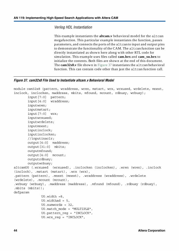
The cam32x8 file shown in Figure 35 instantiates the altcam behavioral function. This can contain code other than just the altcam function call.
Figure 35. cam32x8 File Used to Instantiate altcam Behavioral Function
library ieee;use ieee.std_logic_1164.all;entity cam32x8 is port ( pattern: in std_logic_vector(7 downto 0); wrx: in std_logic_vector(7 downto 0); wrxused: in std_logic; wrdelete: in std_logic; wraddress: in std_logic_vector(4 downto 0); wren: in std_logic; inclock: in std_logic; mstart: in std_logic; mnext: in std_logic; maddress: out std_logic_vector(4 downto 0); mbits: out std_logic_vector(31 downto 0); matchfound: out std_logic; mcount: out std_logic_vector(4 downto 0); rdbusy: out std_logic; wrbusy: out std_logic );end cam32x8; architecture apex of cam32x8 iscomponent altcam generic ( width: positive; widthad: positive; numwords: natural := 0; lpm_file: string := "UNUSED"; lpm_filex: string := "UNUSED"; match_mode: string := "SINGLE"; output_reg: string := "UNREGISTERED"; output_aclr: string := "OFF"; pattern_reg: string := "INCLOCK"; pattern_aclr: string := "Off"; wraddress_aclr: string := "Off"; wrx_reg: string := "INCLOCK"; wrx_aclr: string := "off";
wrcontrol_aclr: string := "OFF" ); port ( pattern: in std_logic_vector(width -1 downto 0); wrx: in std_logic_vector(width -1 downto 0);
40 Altera Corporation
AN 119: Implementing High-Speed Search Applications with Altera CAM
wrxused: in std_logic; wrdelete: in std_logic; wraddress: in std_logic_vector(widthad-1 downto 0); wren: in std_logic; inclock: in std_logic; inclocken: in std_logic := '1'; inaclr: in std_logic := '0'; mstart: in std_logic; mnext: in std_logic; outclock: in std_logic := '0'; outclocken: in std_logic := '1'; outaclr: in std_logic := '0'; maddress: out std_logic_vector(widthad-1 downto 0); mbits: out std_logic_vector(numwords-1 downto 0); mfound: out std_logic; mcount: out std_logic_vector(widthad-1 downto 0); rdbusy: out std_logic; wrbusy: out std_logic );end component;beginU0: altcam generic map (width => 8, widthad => 5, lpm_file => "cam.hex", lpm_filex => "cam_xu.hex", numwords => 32, match_mode => "MULTIPLE", output_reg => "UNREGISTERED")port map (pattern => pattern, wrx => wrx, wrxused => wrxused,wrdelete => wrdelete, wraddress => wraddress, wren => wren, inclock => inclock, mstart => mstart, mnext => mnext, maddress => maddress, mbits => mbits, mfound => matchfound, mcount => mcount, rdbusy => rdbusy, wrbusy => wrbusy );end apex;
Altera Corporation 41

AN 119: Implementing High-Speed Search Applications with Altera CAM
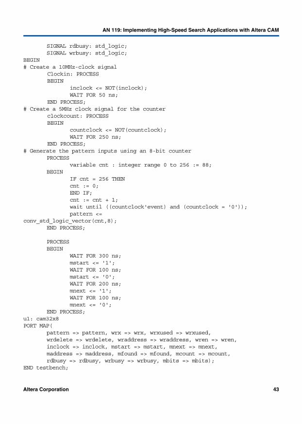
Testbench for 32 × 8 CAM in VHDL
cam_testbench.vhd shown in Figure 36 is an example testbench that demonstrates the functionality of the altcam in multiple-match mode with “don’t care” bits.
Figure 36. cam_testbench.vhd File
LIBRARY ieee;USE ieee.std_logic_1164.ALL;USE ieee.std_logic_arith.ALL;USE std.textio.ALL;ENTITY CAM_testbench ISEND CAM_testbench;ARCHITECTURE testbench OF CAM_testbench ISSIGNAL countclock:std_logic := '0';COMPONENT cam32x8 PORT( pattern: in std_logic_vector(7 downto 0); wrx: in std_logic_vector(7 downto 0); wrxused: in std_logic; wrdelete: in std_logic; wraddress: in std_logic_vector(4 downto 0); wren: in std_logic; inclock: in std_logic; mstart: in std_logic; mnext: in std_logic; maddress: out std_logic_vector(4 downto 0); mbits: out std_logic_vector(31 downto 0); mfound: out std_logic; mcount: out std_logic_vector(4 downto 0); rdbusy: out std_logic; wrbusy: out std_logic );END COMPONENT;
SIGNAL pattern : std_logic_vector(7 downto 0) := "00000000"; SIGNAL wrx: std_logic_vector(7 downto 0) := "00000000";SIGNAL wrxused: std_logic := '0';SIGNAL wrdelete: std_logic := '0';SIGNAL wraddress: std_logic_vector(4 downto 0) := "00000";SIGNAL wren: std_logic := '0';SIGNAL inclock: std_logic := '1';SIGNAL mstart: std_logic := '0';SIGNAL mnext: std_logic := '0';SIGNAL maddress: std_logic_vector(4 downto 0);SIGNAL mbits: std_logic_vector(31 downto 0);SIGNAL mfound: std_logic;SIGNAL mcount: std_logic_vector(4 downto 0);
42 Altera Corporation
AN 119: Implementing High-Speed Search Applications with Altera CAM
SIGNAL rdbusy: std_logic;SIGNAL wrbusy: std_logic;
BEGIN# Create a 10MHz-clock signal
Clockin: PROCESSBEGIN
inclock <= NOT(inclock);WAIT FOR 50 ns;
END PROCESS;# Create a 5MHz clock signal for the counter
clockcount: PROCESSBEGIN
countclock <= NOT(countclock);WAIT FOR 250 ns;
END PROCESS;# Generate the pattern inputs using an 8-bit counter
PROCESSvariable cnt : integer range 0 to 256 := 88;
BEGINIF cnt = 256 THENcnt := 0;END IF;cnt := cnt + 1;wait until ((countclock'event) and (countclock = '0'));pattern <=
conv_std_logic_vector(cnt,8);END PROCESS;
PROCESSBEGIN
WAIT FOR 300 ns;mstart <= '1';WAIT FOR 100 ns;mstart <= '0';WAIT FOR 200 ns;mnext <= '1';WAIT FOR 100 ns;mnext <= '0';
END PROCESS;u1: cam32x8PORT MAP(
pattern => pattern, wrx => wrx, wrxused => wrxused,wrdelete => wrdelete, wraddress => wraddress, wren => wren,inclock => inclock, mstart => mstart, mnext => mnext,maddress => maddress, mfound => mfound, mcount => mcount,rdbusy => rdbusy, wrbusy => wrbusy, mbits => mbits);
END testbench;
Altera Corporation 43
AN 119: Implementing High-Speed Search Applications with Altera CAM
Verilog HDL Instantiation
This example instantiates the altcam.v behavioral model for the altcam megafunction. This particular example instantiates the function, passes parameters, and connects the ports of the altcam to input and output pins to demonstrate the functionality of the CAM. The altcam function can be directly instantiated as shown here along with other RTL code for simulation. This example uses files called cam.hex and cam_xu.hex to initialize the contents. Both files are shown at the end of this document. The cam32x8.v file shown in Figure 37 instantiates the altcam behavioral function. This can contain code other than just the altcam function call.
Figure 37. cam32x8 File Used to Instantiate altcam.v Behavioral Model
module cam32x8 (pattern, wraddress, wren, mstart, wrx, wrxused, wrdelete, mnext, inclock, inclocken, maddress, mbits, mfound, mcount, rdbusy, wrbusy);
input[7:0] pattern;input[4:0] wraddress;inputwren;inputmstart;input[7:0] wrx;inputwrxused;inputwrdelete;inputmnext;inputinclock;inputinclocken;//inputinaclr;output[4:0] maddress;output[31:0] mbits;outputmfound;output[4:0] mcount;outputrdbusy;outputwrbusy;
altcamU0 (.wrxused (wrxused), .inclocken (inclocken), .wren (wren), .inclock (inclock), .mstart (mstart), .wrx (wrx),.pattern (pattern), .mnext (mnext), .wraddress (wraddress), .wrdelete (wrdelete), .mcount (mcount),.wrbusy (wrbusy), .maddress (maddress), .mfound (mfound), .rdbusy (rdbusy), .mbits (mbits));defparam
U0.width =8,U0.widthad = 5,U0.numwords = 32,U0.match_mode = "MULTIPLE",U0.pattern_reg = "INCLOCK",U0.wrx_reg = "INCLOCK",
44 Altera Corporation
AN 119: Implementing High-Speed Search Applications with Altera CAM
U0.pattern_aclr = "Off",U0.wrx_aclr = "Off",U0.wrcontrol_aclr = "Off",U0.wraddress_aclr = "Off",U0.output_aclr = "Off",U0.lpm_file = "cam.hex",U0.lpm_filex = "cam_xu.hex";
endmodule
Verilog HDL Testbench
The Verilog HDL testbench demonstrates the functionality of the altcam megafunction. If the Modelsim simulator is used with the Verilog HDL model and hexadecimal initialization files, compile the design before running the simulation. The convert_hex2ver utility converts the hexadecimal initialization files to a usable format when simulating Verilog HDL code. The following steps describe how this conversion is done.
� Obtain the convert_hex2ver.c and convert_hex2ver_lib.c files from the Altera web site at http://www.altera.com.
� Compile and link the source code into a library.
The following example code shows how to compile the source code within Microsoft Visual C/C++ (version 4.1 and higher) on the Windows NT/98/95 operating systems.
cl -c -I<modelsim_dir>\include convert_hex2ver.c convert_hex2ver_lib.clink -dll -export:init_usertfs convert_hex2ver.obj convert_hex2ver_lib.obj <modelsim_dir>\win32\mtipli.lib
The following example code shows how to compile the source code with Sun C compiler on Solaris.
gcc -c -I<modelsim_dir>/include convert_hex2ver.c convert_hex2ver_lib.cld -G -B symbolic -o convert_hex2ver.so convert_hex2ver.o convert_hex2ver_lib.o
Modify modelsim.ini under the [vsim] section. For Windows NT/98/95 operating systems, add the following line of code:
veriuser = <DLL_dir>\convert_hex2ver.dll
For the Sun C compiler on Solaris, add the following line of code:
veriuser = <SO_dir>/convert_hex2ver.so
Altera Corporation 45

AN 119: Implementing High-Speed Search Applications with Altera CAM
The cam_testbench.v code in Figure 38 shows an example testbench that demonstrates the functionality of the altcam megafunction in multiple-match mode with “don’t care” bits.
Figure 38. cam_testbench.v File
`timescale 1 ps / 1 ps
module cam_testbench();
wire [7:0] pattern;reg [7:0] wrx;reg wrxused;reg wrdelete;reg [4:0] wraddress;reg wren;reg inclock;reg inclocken;reg mstart;reg mnext;wire [4:0] maddress;wire [31:0] mbits;wire mfound;wire [4:0] mcount;wire rdbusy;wire wrbusy;
reg [6:0] cnt;reg clock_count;
cam32x8 L0(.pattern(pattern), .wrx(wrx), .wrxused(wrxused), .wrdelete(wrdelete), .wraddress(wraddress), .wren(wren), .inclock(inclock), .mstart(mstart), .mnext(mnext), .maddress(maddress), .mbits(mbits), .mfound(mfound), .mcount(mcount), .rdbusy(rdbusy), .wrbusy(wrbusy), .inclocken(inclocken));
initialbegin
assign inclocken = 1'b1;wrmask = 8'b00000000;wrmaskused = 1'b0;wrdelete = 1'b0;mstart = 1'b0;mnext = 1'b0;
end
46 Altera Corporation

AN 119: Implementing High-Speed Search Applications with Altera CAM
initial cnt = 88;assign pattern = cnt;
initialbegin
inclock = 1'b0;forever #50000 inclock = ~inclock;
end
initialbegin
clock_count = 1'b0;forever #250000 clock_count = ~clock_count;
end
always@(posedge clock_count)begin
if (cnt == 256)cnt = 0;
cnt = cnt + 1;end
initialbegin
mstart = 1'b0;mnext = 1'b0;#300000 mstart = 1'b1;#100000 mstart = 1'b0;#200000 mnext = 1'b1;#100000 mnext = 1'b0;
end
endmodule
Initialization file (cam.hex) for 32 × 8 bit CAM
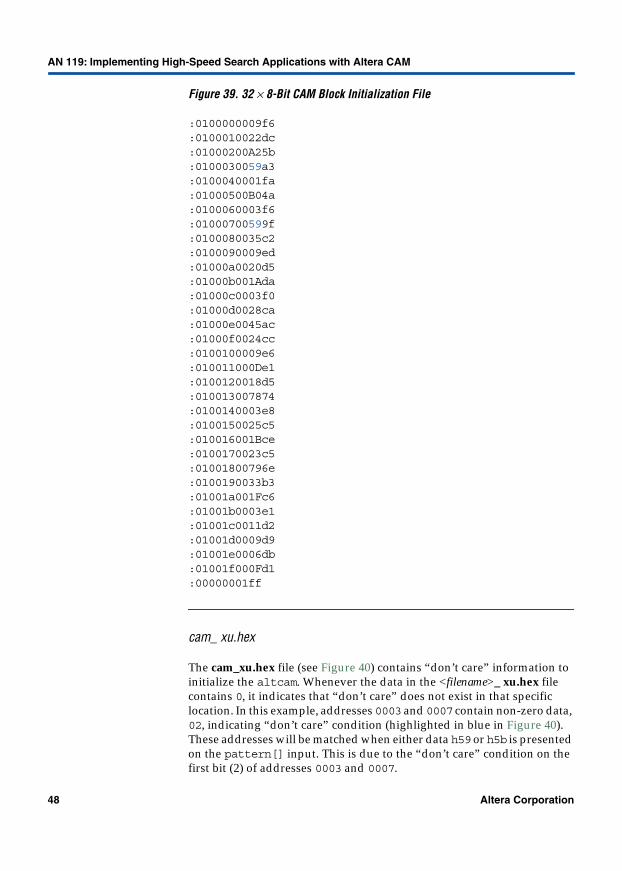
The cam.hex file contains the data to initialize the altcam. Note that addresses 0003 and 0007 contain the same data 59 (highlighted in blue in Figure 39). This indicates that multiple match exists in this example.
Figure 39 shows the initialization file (cam.hex) for a 32-word × 8-bit CAM block:
Altera Corporation 47
AN 119: Implementing High-Speed Search Applications with Altera CAM
Figure 39. 32 × 8-Bit CAM Block Initialization File
:0100000009f6:0100010022dc:01000200A25b:0100030059a3:0100040001fa:01000500B04a:0100060003f6:01000700599f:0100080035c2:0100090009ed:01000a0020d5:01000b001Ada:01000c0003f0:01000d0028ca:01000e0045ac:01000f0024cc:0100100009e6:010011000De1:0100120018d5:010013007874:0100140003e8:0100150025c5:010016001Bce:0100170023c5:01001800796e:0100190033b3:01001a001Fc6:01001b0003e1:01001c0011d2:01001d0009d9:01001e0006db:01001f000Fd1:00000001ff
cam_ xu.hex
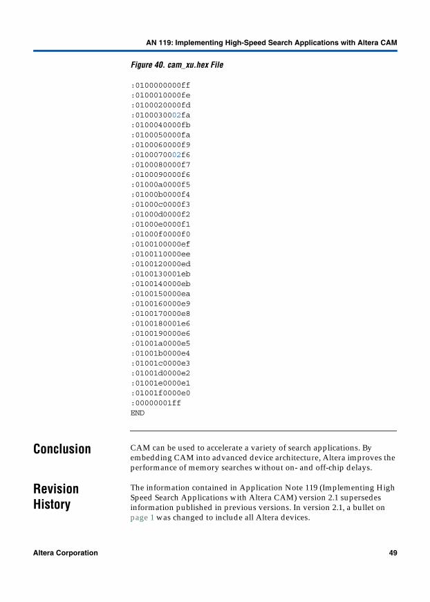
The cam_xu.hex file (see Figure 40) contains “don’t care” information to initialize the altcam. Whenever the data in the <filename>_ xu.hex file contains 0, it indicates that “don’t care” does not exist in that specific location. In this example, addresses 0003 and 0007 contain non-zero data, 02, indicating “don’t care” condition (highlighted in blue in Figure 40). These addresses will be matched when either data h59 or h5b is presented on the pattern[] input. This is due to the “don’t care” condition on the first bit (2) of addresses 0003 and 0007.
48 Altera Corporation
AN 119: Implementing High-Speed Search Applications with Altera CAM
Altera Corporation 49
Figure 40. cam_xu.hex File
:0100000000ff:0100010000fe:0100020000fd:0100030002fa:0100040000fb:0100050000fa:0100060000f9:0100070002f6:0100080000f7:0100090000f6:01000a0000f5:01000b0000f4:01000c0000f3:01000d0000f2:01000e0000f1:01000f0000f0:0100100000ef:0100110000ee:0100120000ed:0100130001eb:0100140000eb:0100150000ea:0100160000e9:0100170000e8:0100180001e6:0100190000e6:01001a0000e5:01001b0000e4:01001c0000e3:01001d0000e2:01001e0000e1:01001f0000e0:00000001ffEND
Conclusion CAM can be used to accelerate a variety of search applications. By embedding CAM into advanced device architecture, Altera improves the performance of memory searches without on- and off-chip delays.
Revision History
The information contained in Application Note 119 (Implementing High Speed Search Applications with Altera CAM) version 2.1 supersedes information published in previous versions. In version 2.1, a bullet on page 1 was changed to include all Altera devices.
AN 119: Implementing High-Speed Search Applications with Altera CAM
®
Altera, APEX, APEX 20K, APEX 20KC, APEX 20KE, APEX II, MegaWizard, Quartus, and Quartus II aretrademarks and/or service marks of Altera Corporation in the United States and other countries. Alteraacknowledges the trademarks of other organizations for their respective products or services mentioned in thisdocument. Altera products are protected under numerous U.S. and foreign patents and pending applications,maskwork rights, and copyrights. Altera warrants performance of its semiconductor products to currentspecifications in accordance with Altera’s standard warranty, but reserves the right to make changes to anyproducts and services at any time without notice. Altera assumes no responsibility or liabilityarising out of the application or use of any information, product, or service described hereinexcept as expressly agreed to in writing by Altera Corporation. Altera customers are advisedto obtain the latest version of device specifications before relying on any publishedinformation and before placing orders for products or services.
Copyright 2001 Altera Corporation. All rights reserved.
101 Innovation DriveSan Jose, CA 95134(408) 544-7000http://www.altera.comApplications Hotline:(800) 800-EPLDCustomer Marketing:(408) 544-7104Literature Services:(888) [email protected]
50 Altera Corporation
Printed on Recycled Paper.