an-2081 lmh6517eval-r1 evaluation board (rev. b)
TRANSCRIPT

User's GuideSNOA553B–October 2010–Revised May 2013
AN-2081 LMH6517EVAL-R1 Evaluation Board
Figure 1. LMH6517EVAL-R1 Evaluation Board
1 General Description
The LMH6517EVAL-R1 evaluation board is designed to aid in the characterization of Texas Instruments'High Speed LMH6517 Digital Controlled Variable Gain Amplifier (DVGA).
The evaluation board is used as a guide for high frequency layout and as a tool to aid in device testingand characterization.
2 Basic Operation
The LMH6517 DVGA has differential inputs and differential outputs. To aid evaluation with 50Ω, singleended test equipment the LMH6517EVAL-R1 evaluation board is shipped with transformers on both theinput and output signal paths. The single ended signal path uses the IN+ and OUT+ marked connectors.The IN− and OUT− signal paths are grounded and the SMA connectors are not installed.
All trademarks are the property of their respective owners.
1SNOA553B–October 2010–Revised May 2013 AN-2081 LMH6517EVAL-R1 Evaluation BoardSubmit Documentation Feedback
Copyright © 2010–2013, Texas Instruments Incorporated

Basic Operation www.ti.com
The input and output pins of the LMH6517 will self bias to approximately mid supply (2.5V). TheLMH6517EVAL-R1 board has been designed with AC coupling on both input and output signal paths toprotect test equipment and to ensure proper operation of the LMH6517 DVGA. Any modifications to theboard should preserve the operating points of the DVGA and protect sensitive test equipment.
Transformers T1– T4 can provide both impedance matching as well as single ended to differentialconversion. The board is shipped with 2:1 turns ratio (4:1 impedance ratio) transformers that will match50Ω equipment with the 200Ω input impedance of the LMH6517 DVGA . Do not connect the transformersecondary winding directly to ground since this will short the DVGA input voltage to ground.
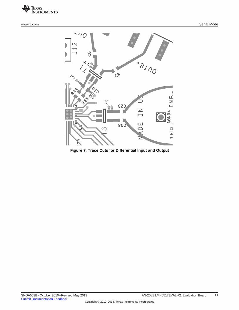
For differential operation the board must be modified by hand. The copper on the grounded input must becut as illustrated in Figure 7. and additional SMA connectors need to be soldered to the board to completethe IN- and OUT- signal paths. The LMH6517EVAL-R1 Evaluation board is 0.63” thick and uses edgemounted SMA connectors. The board is built with Emerson part #142–0701–806 end launch, nickel platedSMA connectors.
The LMH6517EVAL-R1 evaluation board comes built with 1:1 balun transformers and 10 Ohm seriesoutput resistors (R42, R43, R44 and R45). A 4.7pF load capacitor is placed between the resistors and thetransformer (C14 and C15). The 10 Ohm resisters and 4.7pF capacitor form a snubber circuit that reduceshigh frequency peaking and enhances stability. The combination of the snubber circuit and the 1:1 balungives very good power gain and very good OIP3 performance when driving 50Ω test equipment. Theoutput impedance of the LMH6517 amplifier is very low (<2Ω @ 50MHz). Many load conditions can beachieved by changing out the components on the evaluation board. Not all load conditions will require asnubber circuit, but it should be included in the final circuit design unless sufficient testing has shown it tobe unnecessary.
The capacitors C5, C7, C8 and C9 isolate the output transformer from the output SMA connectors and arenot required if the transformer provides DC blocking. The spaces marked C34, C35, C36 and C37 are leftempty by the factory. These positions are included to provide the flexibility to add extra components.Capacitors can be added to create a low pass filter. Resistors could be placed in these locations to createdifferent load conditions for the amplifier.
2 AN-2081 LMH6517EVAL-R1 Evaluation Board SNOA553B–October 2010–Revised May 2013Submit Documentation Feedback
Copyright © 2010–2013, Texas Instruments Incorporated

www.ti.com Basic Operation
Figure 2. Output Schematic
3SNOA553B–October 2010–Revised May 2013 AN-2081 LMH6517EVAL-R1 Evaluation BoardSubmit Documentation Feedback
Copyright © 2010–2013, Texas Instruments Incorporated

Using with Different Sources or Loads www.ti.com
Figure 3. Input Schematic
The board was designed to be very flexible for many different configurations. Zoomed in portions of theinput and output schematics are shown above in Figure 2 and Figure 3. The evaluation board, as shipped,has been optimized for ease of use with single ended 50 Ohm test equipment. This configuration may notemulate the most common application circuits. The signal path schematic is shown in Figure 8 and the fullschematic in . PDF format is available upon request.
3 Using with Different Sources or Loads
The LMH6517EVAL-R1 evaluation board supports differential operation on both inputs and outputs.However they will require additional components and some board rework. For driving the evaluation boardfrom a differential source, symmetrical signal paths are provided. Both input and output paths support fullydifferential test equipment.
To drive the LMH6517EVAL-R1 evaluation board from a differential source, the transformers T3 and T4must be removed. The diagrams in Figure 6 and Figure 7 show the required connections for differentialinputs. DC coupled operation is possible using differential signals. For DC coupled operation, make surethat the test equipment can provide the 2.5 V offset voltage required.
For differential output signals remove transformers T1 and T2. Wire jumpers or zero Ohm resistors mustbe added to complete the signal path across the transformer pads similar to the changes required fordifferential inputs.
4 Other Board Configurations
For other applications or experiments there are many options for changing the output circuit to simulatedifferent circuit conditions. One option is to use a 2:1 transformer to simulate high impedance loads. In thiscase one would use 100 Ohm resistors for R42, R43, R44 and R45. This would present a load of 200Ohms to the amplifier output. Many common filter circuits have 200 Ohm input impedance. Othercombinations can also be used to simulate different load conditions. With a high impedance load thecapacitors C14 and C15 should be decreased to 1pF to avoid losing bandwidth.
4 AN-2081 LMH6517EVAL-R1 Evaluation Board SNOA553B–October 2010–Revised May 2013Submit Documentation Feedback
Copyright © 2010–2013, Texas Instruments Incorporated

www.ti.com Additional Design Tools
Near the power connector are a number of 0.1” pitch headers. The header labeled J1 provides off boardaccess to the LMH6517 digital control pins. The J1 pins and functions are described below. The jacklabeled J10 is normally loaded with a shorting jumper, it provides power to a 3.3V power supply used toprovide 3.3V logic signals to the digital pins. The jack labeled J11 is also loaded with a shorting block andit provides the 5V power to the LMH6517. By removing the short on this jack and replacing it with anammeter the current drawn by the DVGA can be measured. The jack labeled J12 is a ground connectorand is normally left empty.
5 Additional Design Tools
The RD-179: High-IF Sub-sampling Receiver Subsystem board (SP16160CH1RB) is also available. Thisreference design includes the ADC16DV160 ADC, the LMH6517 DVGA, and the LMK04031B precisionclock conditioner. Power regulation, filters and controlled impedance board layout are all provided in thisreference design. Please visit the TI website, www.ti.com for further details.
6 Gain Control
The LMH6517 DVGA has three control modes including, parallel mode, serial (SPI compatible) mode andpulse mode. Parallel and pulse modes are fully supported on the board. Serial mode control requires theuse of a PC and the SPUSI2 USB to SPI interface board (available separately) or an external signalsource like a logic analyzer or a microcontroller. Each of the control modes is detailed fully below.
Mode SW1 Mode SW2 Gain Setting(MOD1) (MOD0)
Off Off Parallel
Off On Serial
On Off Pulse
7 Parallel Mode
For ease of use, dip switches are provided to set the LMH6517 gain in parallel mode. This mode is theeasiest to use for basic measurements. To set the board in parallel mode, Dip-switch SW 1 which islabeled MODE must be set such that the top switch is in the OFF position and the bottom switch is in theOFF position (the top of the board is the Channel A portion). To move the MODE switches to the OFFposition, slide them toward the output SMA connectors.
In Parallel mode, the switch banks are used to set the gain of the DVGA. When using the DIP switches tochange gain in parallel mode ensure that the switch labeled LATA or LATB is in the ON position. With thelatch switch in the ON state the device is in transparent mode and any change in the dip switches isimmediately reflected in the device gain. Moving the latch pin switch to the OFF position holds the lastgain setting and ignores changes in the gain control switches. When the latch switch is in the OFF positionthe dip switches that control the gain can be configured as desired and then implemented by momentarilyswitching the LATA or LATB switch. For detailed instructions on the pin functions see Low Power, LowNoise, IF and Baseband, Dual 16 bit ADC Driver With Digitally Controlled Gain Data Sheet (SNOSB19)
In parallel mode, the DIP switch banks SWGA and SWGB are used to set the gain of the DVGA. The gainbits are binary weighted with the LSB representing a 0.5dB gain step and the MSB representing a 16dBstep. The steps increase the gain when the switch is in the ON position. For example, switching B5 fromOFF to ON will increase the gain by 16dB. Between the Gain control bits and the Latch switch is anenable (ENA or ENB) switch. Setting this switch to the OFF position Enables the respective DVGAchannel.
8 Pulse Mode
The DVGA is also very easy to control in Pulse mode. For system implementations Pulse mode requiresfewer digital control lines than parallel mode at the expense of gain control speed. To use Pulse Mode theMode switches should be set such that MODE 1 is in the ON position and MODE2 is in the OFF position.Gain changes are accomplished by using the UP and DN buttons. There are separate buttons for the Achannel and the B channel. Gain will be indicated on the LED displays.
5SNOA553B–October 2010–Revised May 2013 AN-2081 LMH6517EVAL-R1 Evaluation BoardSubmit Documentation Feedback
Copyright © 2010–2013, Texas Instruments Incorporated

Serial Mode www.ti.com
The dip switches that are used to control gain in parallel mode have different functions in Pulse mode.SWA, which controls the A channel should be set with the A4, A3, ENA and LATA positions in the OFFsetting. The positions marked A5 and A0 need to be in the ON position. The positions marked A2 and A1are used to set the DVGA gain step size.
Table 1. SWG Switch Settings for Pulse Mode
SWGA A5 A4 A3 A2 A1 A0 ENBA LATA
SWGB B5 B4 B3 B2 B1 B0 ENBB LATB
Position ON OFF OFF A/R A/R ON OFF OFF
The switch marked SWB controls the B channel and should be configured as follows: positions markedB4, B3, ENB and LATB set to OFF, the positions marked B5 and B0 need to be in the ON position. Thepositions marked B2 and B1 set the channel B gain step size. See the product data sheet for step sizeoptions. Note that if the switch marked B5 on SWGB is in the Off position the entire amplifier will be in anundefined state and will not operate correctly.
The push button switches located between the DVGA and the Parallel DIP switch banks are for use inpulse mode. The UPA and UPB buttons increment the gain up one step while the DNA and DNB buttonsdecrement the gain by one step. The gain step sizes are set by the DIP switches labeled S1 and S0 onthe parallel control DIP switches. Each channel can have a different gain step size.
Table 2. Pulse Mode Gain Step SizesS1 and S0 are Located in SWGA and SWGB
S1 S0 Gain Step Size
On On 0.5dB
On Off 1dB
Off On 2dB
Off Off 6dB
9 Serial Mode
Serial mode is the most complex control mode and is considerably slower than parallel mode, but it is veryflexible and requires fewer digital control lines. To use Serial Mode the Mode switches should be set suchthat MODE 1 is in the OFF position and MODE2 is in the ON position. Note that if the switch marked B5on SWGB is in the Off position the entire amplifier will be in an undefined state and will not operatecorrectly.
Serial mode requires external logic, either from a microcontroller or logic analyzer. A 0.1” header strip islocated near SWGA (J1). This strip can be used to connect a microcontroller or logic analyzer to the serialcontrol pins, the pulse control pins and the channel A parallel control pins. The header pin functions areshown in the table below. Please refer to the product data sheet for the full description of these pinfunctions.
Please note that the SWGA dip switches will impact the on-board impedance for the J1 header pins. If theSWGA dip switches are set to the OFF position, there is no on-board termination for the J1 header pinsand they will appear as high impedance to the logic analyzer. Make sure that this does not result in logicsignals that are beyond the absolute maximum rating for the LMH6517. When the SWGA dip switches arein the ON position there are 50Ω resistors to ground connected the header pins in parallel with theLMH6517 logic pins. Some digital sources are unable to drive this load condition. If it seems that theLMH6517 is not responding to digital control signals this could be one cause.
To aid in the evaluation of SPI controlled devices, TI manufactures the SPUSI2 board and provides theTinyI2CSPI software to control it. The software and the SPUSI2 evaluation board kit can be ordered fromthe TI website. The software is Windows® compatible. The first step for using the board in serial mode isto place the MODE switches in the proper configuration. The MODE1 switch will be in the OFF positionand the MODE2 switch will be in the ON position. Directions for installing the USB control software andevaluation board drivers are in the user's guide available on the TI website.
6 AN-2081 LMH6517EVAL-R1 Evaluation Board SNOA553B–October 2010–Revised May 2013Submit Documentation Feedback
Copyright © 2010–2013, Texas Instruments Incorporated

www.ti.com Serial Mode
Once the SPUSI2 board drivers and TinyI2CSPI software are installed, the appropriate pins on theLMH6517 board need to be connected to the SPUSI2 board. Soldering jumpers is one easy method.Connect the CLK, SDI and CS pins as well as a ground wire to the SPUSI2 board. The board softwareshould be set to SPI mode and the CS adn CKPOL columns should be set to 1. The CKPHA columnneeds to be set to 1and the number of bits should be set to 16. Check to the LMH6517 data sheet fordetails on the data to be sent to the DVGA registers. Some simple SPI commands, as well as the propersoftware settings are shown below in Figure 9.
Table 3. Header Jack Pin Assignments (J1)
Header Pin LMH6517 Pin # Parallel Function Serial Function Pulse Function
J1–1 3 Address bit 5 N/A N/A
J1–2 2 Address bit 4 CLK Up A
J1–3 1 Address bit 3 Serial Data In Down A
J1–4 32 Address bit 2 Chip Select Step Size MSB
J1–5 31 Address bit 1 Serial Data Out Step Size LSB
J1–6 25 Address bit 0 N/A N/A
J1–7 22 Enable A Enable A Enable A
J1–8 21 Latch A N/A N/A
J1–9 N/A Ground Ground Ground
7SNOA553B–October 2010–Revised May 2013 AN-2081 LMH6517EVAL-R1 Evaluation BoardSubmit Documentation Feedback
Copyright © 2010–2013, Texas Instruments Incorporated

Serial Mode www.ti.com
Figure 4. Evaluation Board Top Layer
8 AN-2081 LMH6517EVAL-R1 Evaluation Board SNOA553B–October 2010–Revised May 2013Submit Documentation Feedback
Copyright © 2010–2013, Texas Instruments Incorporated

www.ti.com Serial Mode
Figure 5. Evaluation Board Bottom Layer
9SNOA553B–October 2010–Revised May 2013 AN-2081 LMH6517EVAL-R1 Evaluation BoardSubmit Documentation Feedback
Copyright © 2010–2013, Texas Instruments Incorporated

Serial Mode www.ti.com
Figure 6. Connections for Differential Input
10 AN-2081 LMH6517EVAL-R1 Evaluation Board SNOA553B–October 2010–Revised May 2013Submit Documentation Feedback
Copyright © 2010–2013, Texas Instruments Incorporated
www.ti.com Serial Mode
Figure 7. Trace Cuts for Differential Input and Output
11SNOA553B–October 2010–Revised May 2013 AN-2081 LMH6517EVAL-R1 Evaluation BoardSubmit Documentation Feedback
Copyright © 2010–2013, Texas Instruments Incorporated

Serial Mode www.ti.com
Figure 8. Signal Path Schematic
12 AN-2081 LMH6517EVAL-R1 Evaluation Board SNOA553B–October 2010–Revised May 2013Submit Documentation Feedback
Copyright © 2010–2013, Texas Instruments Incorporated

www.ti.com Serial Mode
Figure 9. Software Settings for SPI Control
13SNOA553B–October 2010–Revised May 2013 AN-2081 LMH6517EVAL-R1 Evaluation BoardSubmit Documentation Feedback
Copyright © 2010–2013, Texas Instruments Incorporated

IMPORTANT NOTICE
Texas Instruments Incorporated and its subsidiaries (TI) reserve the right to make corrections, enhancements, improvements and otherchanges to its semiconductor products and services per JESD46, latest issue, and to discontinue any product or service per JESD48, latestissue. Buyers should obtain the latest relevant information before placing orders and should verify that such information is current andcomplete. All semiconductor products (also referred to herein as “components”) are sold subject to TI’s terms and conditions of salesupplied at the time of order acknowledgment.
TI warrants performance of its components to the specifications applicable at the time of sale, in accordance with the warranty in TI’s termsand conditions of sale of semiconductor products. Testing and other quality control techniques are used to the extent TI deems necessaryto support this warranty. Except where mandated by applicable law, testing of all parameters of each component is not necessarilyperformed.
TI assumes no liability for applications assistance or the design of Buyers’ products. Buyers are responsible for their products andapplications using TI components. To minimize the risks associated with Buyers’ products and applications, Buyers should provideadequate design and operating safeguards.
TI does not warrant or represent that any license, either express or implied, is granted under any patent right, copyright, mask work right, orother intellectual property right relating to any combination, machine, or process in which TI components or services are used. Informationpublished by TI regarding third-party products or services does not constitute a license to use such products or services or a warranty orendorsement thereof. Use of such information may require a license from a third party under the patents or other intellectual property of thethird party, or a license from TI under the patents or other intellectual property of TI.
Reproduction of significant portions of TI information in TI data books or data sheets is permissible only if reproduction is without alterationand is accompanied by all associated warranties, conditions, limitations, and notices. TI is not responsible or liable for such altereddocumentation. Information of third parties may be subject to additional restrictions.
Resale of TI components or services with statements different from or beyond the parameters stated by TI for that component or servicevoids all express and any implied warranties for the associated TI component or service and is an unfair and deceptive business practice.TI is not responsible or liable for any such statements.
Buyer acknowledges and agrees that it is solely responsible for compliance with all legal, regulatory and safety-related requirementsconcerning its products, and any use of TI components in its applications, notwithstanding any applications-related information or supportthat may be provided by TI. Buyer represents and agrees that it has all the necessary expertise to create and implement safeguards whichanticipate dangerous consequences of failures, monitor failures and their consequences, lessen the likelihood of failures that might causeharm and take appropriate remedial actions. Buyer will fully indemnify TI and its representatives against any damages arising out of the useof any TI components in safety-critical applications.
In some cases, TI components may be promoted specifically to facilitate safety-related applications. With such components, TI’s goal is tohelp enable customers to design and create their own end-product solutions that meet applicable functional safety standards andrequirements. Nonetheless, such components are subject to these terms.
No TI components are authorized for use in FDA Class III (or similar life-critical medical equipment) unless authorized officers of the partieshave executed a special agreement specifically governing such use.
Only those TI components which TI has specifically designated as military grade or “enhanced plastic” are designed and intended for use inmilitary/aerospace applications or environments. Buyer acknowledges and agrees that any military or aerospace use of TI componentswhich have not been so designated is solely at the Buyer's risk, and that Buyer is solely responsible for compliance with all legal andregulatory requirements in connection with such use.
TI has specifically designated certain components as meeting ISO/TS16949 requirements, mainly for automotive use. In any case of use ofnon-designated products, TI will not be responsible for any failure to meet ISO/TS16949.
Products Applications
Audio www.ti.com/audio Automotive and Transportation www.ti.com/automotive
Amplifiers amplifier.ti.com Communications and Telecom www.ti.com/communications
Data Converters dataconverter.ti.com Computers and Peripherals www.ti.com/computers
DLP® Products www.dlp.com Consumer Electronics www.ti.com/consumer-apps
DSP dsp.ti.com Energy and Lighting www.ti.com/energy
Clocks and Timers www.ti.com/clocks Industrial www.ti.com/industrial
Interface interface.ti.com Medical www.ti.com/medical
Logic logic.ti.com Security www.ti.com/security
Power Mgmt power.ti.com Space, Avionics and Defense www.ti.com/space-avionics-defense
Microcontrollers microcontroller.ti.com Video and Imaging www.ti.com/video
RFID www.ti-rfid.com
OMAP Applications Processors www.ti.com/omap TI E2E Community e2e.ti.com
Wireless Connectivity www.ti.com/wirelessconnectivity
Mailing Address: Texas Instruments, Post Office Box 655303, Dallas, Texas 75265Copyright © 2013, Texas Instruments Incorporated