an-9019 motor drive system using spm...
TRANSCRIPT

Application Note 9019
Motor Drive System Using SPM Inverter
October, 2001
Rev. A, October 20011
CONTENTS
1. Introduction
2. SPM-Inverter System Overview2.1 Introduction2.2 Line Filter2.3 Initial Charging Circuit2.4 Dynamic Brake (DB) Circuit2.5 SMPS (Switching Mode Power Supply)
3. SPM Product Guide3.1 Product Line-Up3.2 Ordering Information
4. Induction Motor Drive (V/Hz)
5. BLDC Motor Drive
6. Space Vector Pulse Width Modulation (SVPWM)
7. Real Implementation7.1 Block diagram7.2 Flow Chart7.3 The Extract of the source code

2
Rev. A, October 2001
1. Introduction
The terms “energy-saving” and “quiet-running” are becoming very important in the world ofvariable speed motor drives. Inverter technology is being accepted by a wide range of users inthe design of these products, and their use is increasing.For low-power motor control, there are increasing demands for compactness, built-in control,and lower overall-cost. An important consideration, in justifying the use of inverters in theseapplications, is to optimize the total-cost-performance ratio of the overall drive system. In otherwords, the systems have to be less noisy, more efficient, smaller and lighter, more advanced infunction and more accurate in control with a very low cost.In order to meet these needs, Fairchild has developed a new series of compact, high-function-ality, and high efficiency power semiconductor devices called “SPM (Smart Power Module)”.SPM-based inverters are now considered an attractive alternative to conventional discrete-based inverters for low-power motor drives, specifically for appliances such as washingmachines, air-conditioners etc.SPM combines optimized circuit protection and drive matched to the IGBT’s switching charac-teristics. Highly effective short-circuit current detection/protection is achieved through the useof advanced current sensing IGBT chips that allow continuous monitoring of the IGBT’s cur-rent. System reliability is further enhanced by the integrated under-voltage protection function.The high speed built-in HVIC provides an opto-coupler-less IGBT gate driving capability thatfurther reduces the overall size of the inverter system design. Additionally, the incorporatedHVIC allows the use of a single-supply drive topology without negative bias. It should be notedthat one could build a typical block diagram of an SPM-inverter as shown in Fig. 1.1.Small power drive systems using 3-phase voltage-fed inverters, which are frequently used inhome appliances, are being used in an increasing number of applications. Induction motorsand BLDC motors are mostly used in these drive systems. Induction motors are used moreoften because they have the advantages of price and durability. In home appliances, exceptwhere high performance control is a requirement, the constant V/Hz principle that maintains aconstant ratio between the stator voltage magnitude and the stator voltage frequency is gener-ally used. This keeps the stator magnetic field magnitude constant. The advantage of thismethod is a simple control scheme that allows for the design of a low priced system. TheBLDCM has high output power per volume due to good heat radiation. It also has the merits ofhigh efficiency, low audible noise, and ease of control. The output torque of a trapezoidal backemf (electromotive force) BLDCM is proportional to the motor input current regardless of therotor position. Although the output torque has a ripple component, the BLDCM has a merit thatthe driver can be designed with low cost because the drive circuit is relatively simple. A sinu-soidal back emf BLDCM is frequently applied in precision servo control applications because itdoes not have the output torque ripple. But the drive system can be complicated because thesinusoidal current with respect to the absolute rotor position should be applied to each phase.The simple speed control system of the trapezoidal back emf BLDCM using a hall sensor,which can detect the rotor position, is shown.PWM signals are pulse trains that have a variable width, constant frequency, and a constantmagnitude. A PWM signal has one pulse per one PWM period, and its width varies withrespect to the modulating signal. The frequency of a PWM signal should be greater than thatof a modulating signal. The most frequently used continuous voltage modulation method is thesymmetric PWM, which means that each pulse is symmetric with respect to the PWM period.The offset voltage injection symmetric SVPWM that maximizes the DC link voltage utilization,with a relatively light computation load, is shown.The objective of this application note is to show the details of SPM power circuit design and itsdrive applications to SPM users. This note describes some designs that should enable usersin deploying the SPM expeditiously and shorten their development time. It will make inverterdesigners very familiar with the SPM and help them in incorporating it in their designs.
Rev. A, October 20013
2. SPM-Inverter System Overview
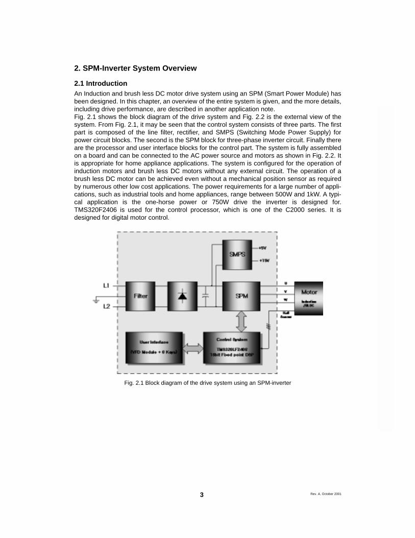
2.1 IntroductionAn Induction and brush less DC motor drive system using an SPM (Smart Power Module) hasbeen designed. In this chapter, an overview of the entire system is given, and the more details,including drive performance, are described in another application note. Fig. 2.1 shows the block diagram of the drive system and Fig. 2.2 is the external view of thesystem. From Fig. 2.1, it may be seen that the control system consists of three parts. The firstpart is composed of the line filter, rectifier, and SMPS (Switching Mode Power Supply) forpower circuit blocks. The second is the SPM block for three-phase inverter circuit. Finally thereare the processor and user interface blocks for the control part. The system is fully assembledon a board and can be connected to the AC power source and motors as shown in Fig. 2.2. Itis appropriate for home appliance applications. The system is configured for the operation ofinduction motors and brush less DC motors without any external circuit. The operation of abrush less DC motor can be achieved even without a mechanical position sensor as requiredby numerous other low cost applications. The power requirements for a large number of appli-cations, such as industrial tools and home appliances, range between 500W and 1kW. A typi-cal application is the one-horse power or 750W drive the inverter is designed for.TMS320F2406 is used for the control processor, which is one of the C2000 series. It isdesigned for digital motor control.
Fig. 2.1 Block diagram of the drive system using an SPM-inverter

4
Rev. A, October 2001
Fig. 2.2 External view of the drive board
The present configuration allows the immediate operation of an induction motor with 750W ofpower on the shaft. An equivalent brush less DC motor requires the proper adjustment of thewire connection located on the motor input part.The inverter can be operated at 220/110V with 50/60Hz. The rectified voltage from the 220Vmains optimally requires a motor with a line-to-line voltage of 220V due to the space-vectorbased PWM method implemented. The rms current amounts to about 3A for providing an out-put power of 750W. Similarly, the current at the 110V mains increases to 6A.The motor control program running on the micro controller is implemented by using a 16 digit *2 line VFD (Vacuum Fluorescent Display) and 6 keys. The keypad allows users to set up theswitching frequency, dead time, acceleration time, deceleration time, base voltage, base fre-quency, frequency reference, torque boost etc. Three kinds of pattern operation are possible.A manually controlled volume also supports the variable speed operation of the motors.
(a) Control board
(b) Control board with BLDC motor
Rev. A, October 20015
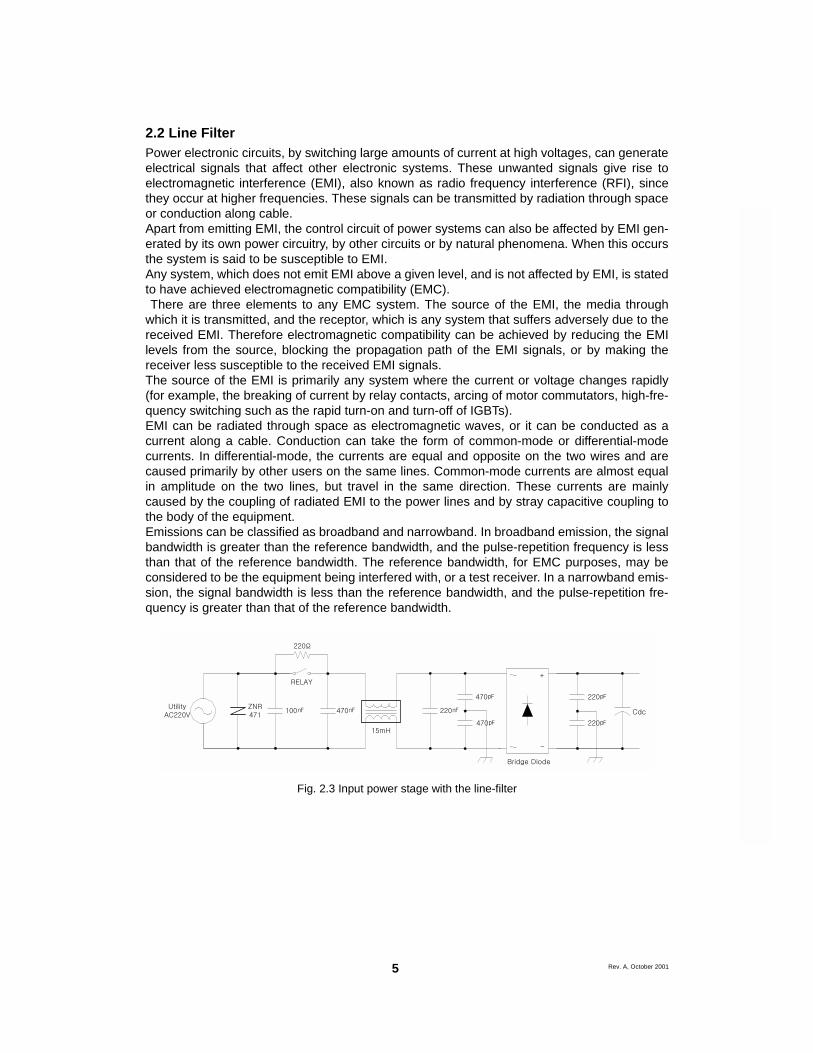
2.2 Line FilterPower electronic circuits, by switching large amounts of current at high voltages, can generateelectrical signals that affect other electronic systems. These unwanted signals give rise toelectromagnetic interference (EMI), also known as radio frequency interference (RFI), sincethey occur at higher frequencies. These signals can be transmitted by radiation through spaceor conduction along cable. Apart from emitting EMI, the control circuit of power systems can also be affected by EMI gen-erated by its own power circuitry, by other circuits or by natural phenomena. When this occursthe system is said to be susceptible to EMI. Any system, which does not emit EMI above a given level, and is not affected by EMI, is statedto have achieved electromagnetic compatibility (EMC). There are three elements to any EMC system. The source of the EMI, the media throughwhich it is transmitted, and the receptor, which is any system that suffers adversely due to thereceived EMI. Therefore electromagnetic compatibility can be achieved by reducing the EMIlevels from the source, blocking the propagation path of the EMI signals, or by making thereceiver less susceptible to the received EMI signals.The source of the EMI is primarily any system where the current or voltage changes rapidly(for example, the breaking of current by relay contacts, arcing of motor commutators, high-fre-quency switching such as the rapid turn-on and turn-off of IGBTs).EMI can be radiated through space as electromagnetic waves, or it can be conducted as acurrent along a cable. Conduction can take the form of common-mode or differential-modecurrents. In differential-mode, the currents are equal and opposite on the two wires and arecaused primarily by other users on the same lines. Common-mode currents are almost equalin amplitude on the two lines, but travel in the same direction. These currents are mainlycaused by the coupling of radiated EMI to the power lines and by stray capacitive coupling tothe body of the equipment.Emissions can be classified as broadband and narrowband. In broadband emission, the signalbandwidth is greater than the reference bandwidth, and the pulse-repetition frequency is lessthan that of the reference bandwidth. The reference bandwidth, for EMC purposes, may beconsidered to be the equipment being interfered with, or a test receiver. In a narrowband emis-sion, the signal bandwidth is less than the reference bandwidth, and the pulse-repetition fre-quency is greater than that of the reference bandwidth.
Fig. 2.3 Input power stage with the line-filter
ZNR471
100 470
RELAY
220Ω
UtilityAC220V
220
470
470
220
Cdc
Bridge Diode
22015mH
+
-

6
Rev. A, October 2001
EMI sources can be broadly divided into two categories, natural and man-made. Naturallycaused EMI, below 10MHz, is mainly due to atmospheric noise resulting from electricalstorms. Above 10MHz they are primarily a result of cosmic noise and solar radiation. Man-made EMI can be intentional or unintentional. It is the variation of the voltage and currentwhich produces EMI, whose magnitude depends on the value of the current, the length of theconductors, the rate of change of the voltage and current, and the physical position of the con-ductors relative to each other and any earth plains.Protection against conducted EMI being transmitted along a cable is achieved by means ofsuppression filters, which consist basically of inductive and capacitive elements. A variety ofsuch filters exist since one type, which suppresses interference completely from one system,may be quite useless in another. The location of the filter is also important. It should generally be placed directly at the source ofinterference, and the output and input leads should never be bundled together. The compo-nents chosen for the filters should also be carefully designed. The inductors must have lowstray capacitors, so they should not be multi-layer, and the capacitors must have low seriesinductance. The filter should be enclosed in a screened box as much as possible. This is con-nected to the wall of the shielded enclosure, so that interference signals from the noisy side donot mix with the quiet side of the system.Fig. 2.3 shows an example of one of the basic filter arrangements, which are used in thedesigned drive system for suppressing the conducted interference. This includes the rectifyingbridge diode, the varistor to suppress an input spike voltage, and the relay circuit for the initialcharging of the DC-link capacitor. It may be noted that there are choke coil and Y-connectedcapacitors against common-mode noise, and AC capacitors against differential-mode noise.
2.3 Initial Charging Circuit On turning on the system power, there would be high current at the system input line. In orderto prevent an over-current damage of the bridge diode and the DC-link capacitor, the initialcharging circuit is designed as shown in Fig. 2.4.
Fig. 2.4 Initial charging circuit
+
-
2N2222
KRC101S
4.7
4.7 U1DL-44A
3.3V 5V
From CPU
CdcUtilityAC220V
Bridge Diode
Relay
5V
220Ω

Rev. A, October 20017
Depending on the bridge diode rating and the electrolytic capacitor maximum ripple current,the relay is driven after 800ms of charging duration from power on. The series resistor con-nected in parallel with the relay should be able to endure the power loss during the chargingperiod. The simulation waveform is shown below.Simulation condition
Load : 1Hp(750W)Input : AC220V, single phaseDC-link capacitors: 470µF/250WV × 2EA connected in seriesCharging resistor: 220Ω/3W
Fig. 2.5 Initial charging simulation
AC input current [A]
DC-link voltage [V]
Charaging resistor power [W]

8
Rev. A, October 2001
2.4 Dynamic Brake (DB) CircuitIn adjustable-speed motor drives, the machines may be subjected to electrical braking forreduction of speed. In electrical braking, the motor is operated in the generating mode and thekinetic energy stored in the system inertia is converted to electrical energy. In the designedsystem a resistor is used to dissipate the energy, which is well known as dynamic brakingresistor. Dynamic braking power depends on thee DC-link voltage and resistor value. The DBresistor used is a 200Ω/200W metal resistor. An IGBT with a rating of 2A/600V is used for theDB. Fig. 2.6 shows the detailed DB circuit.
Fig. 2.6 Dynamic braking circuit of the designed system
2.5 SMPS (Switching Mode Power Supply) The Flyback type of SMPS is designed for the isolated dc-to-dc converter. The detailed sche-matic is shown in Fig. 2.7. It is designed to generate two values of 15V and 5V for control sup-ply, and their current ratings are 0.3A and 0.7A, respectively.For the SMPS control, the adopted main power switch is KA5H0280R made by Fairchild Semi-conductor, and its major specifications are shown in Table 2.1.
Table 2.1 Specification of KA5H0280R
Vdmax [V] Ipeak [A] Pin (max) [W] Fopr [kHz] Rds (on) max [Ω] PKG800 1.2 25 100/70 7.0(Id=1.0A) TO-220F-4L
+
-
KTN2907
2N2222
KRC101S
4.7
4.7 249Ω
10
3.3V 5V
15V
From CPU
200ΩD2U60S
Cdc
G2N60
UtilityAC220V
Bridge Diode

Rev. A, October 20019
Fig. 2.7 SMPS circuit of the designed system
Table 2.2 shows the winding specification for the SMPS transformer. The turn ratio of the pri-mary winding to the secondary one for 5V supply is 120:7. 0.4 copper wire is used for 5V wind-ing and 0.2 copper wire is used for the others. There are 3 turns of 0.050mm thick polyestertaping to ensure that there is insulation between each winding.
Note) NP: Primary winding NFB: Flyback windingN5V: 5V output winding N15V: 15V output winding
Table 2.2 Winding specifications
No. Pin (Start → Finish) Wire Turns Winding MethodNp1 1 → 2 0.20φ × 1 60 Space Winding
Insulation : Polyester Tape t=0.050mm, 3LayerN5V 6 → 7 0.40φ × 1 7 Space Winding
Insulation : Polyester Tape t=0.050mm, 3LayersN15V 6 → 8 0.20φ × 1 17 Space Winding
Insulation : Polyester Tape t=0.050mm, 3LayersNFB 5 → 4 0.20φ × 1 20 Space Winding
Insulation : Polyester Tape t=0.050mm, 3LayersNP2 2 → 3 0.20φ × 1 60 Space Winding
Insulation : Polyester Tape t=0.050mm, 3Layers
Table 2.3 Electrical characteristics of the transformer
Pin Spec. RemarksInductance 1 – 3 1.3mH ± 5% 100kHz, 1VLeakage 1 – 3 120µH (max.) Secondary Short
U1DL-44A
U1DL-44A
100
220
100
220
1
10047
100Cdc
H11A817B
200Ω
H11A817B
TL431A
2.49
2.61
0.1mH
0.1mH
12
10
U1DL-44A 10Ω
UF4007
10
100100500
KA5H0280R
15V
GND
5V
DCN
DCP
F/B
P15
P5
GND
DCNVcc Drain
SPS
GND F/B
10
Rev. A, October 2001
The winding order shown in Fig. 2.8 is applied considering the coupling coefficient.
Fig. 2.8 The winding order (EI2218 core and bobbin are used)
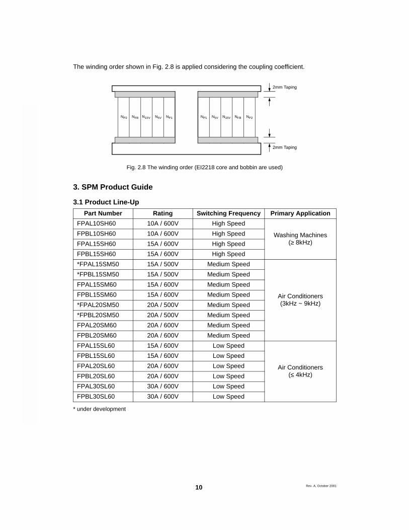
3. SPM Product Guide
3.1 Product Line-Up
* under development
Part Number Rating Switching Frequency Primary ApplicationFPAL10SH60 10A / 600V High Speed
Washing Machines(≥ 8kHz)
FPBL10SH60 10A / 600V High SpeedFPAL15SH60 15A / 600V High SpeedFPBL15SH60 15A / 600V High Speed*FPAL15SM50 15A / 500V Medium Speed
Air Conditioners(3kHz ~ 9kHz)
*FPBL15SM50 15A / 500V Medium SpeedFPAL15SM60 15A / 600V Medium SpeedFPBL15SM60 15A / 600V Medium Speed*FPAL20SM50 20A / 500V Medium Speed*FPBL20SM50 20A / 500V Medium SpeedFPAL20SM60 20A / 600V Medium SpeedFPBL20SM60 20A / 600V Medium SpeedFPAL15SL60 15A / 600V Low Speed
Air Conditioners(≤ 4kHz)
FPBL15SL60 15A / 600V Low SpeedFPAL20SL60 20A / 600V Low SpeedFPBL20SL60 20A / 600V Low SpeedFPAL30SL60 30A / 600V Low SpeedFPBL30SL60 30A / 600V Low Speed
NFB N15V N5V NP1NP2 NP1 N5V N15V NFB NP2
2mm Taping
2mm Taping

Rev. A, October 200111
3.2 Ordering Information
FPAL15SH60Voltage Rating ( x 10)
H: High Switching FrequencyM: Medium Switching FrequencyL: Low Switching Frequency
S: Single-Grounded Power SupplyM: Multi-Grounded Power Supply
Current Rating
L: Package Type
P: Power Circuit Type
Fairchild Semiconductor
A: Option for Built-In ThermistorB: Option for No-Thermistor

12
Rev. A, October 2001
4. Induction Motor Drive (V/Hz)
Fig. 4.1 Single-phase equivalent circuit of a polyphase induction motor
The fundamental steady-state equivalent circuit of the induction motor is shown in Fig. 4.1.The rotating airgap flux induces an emf (electromotive force), E1, in the stator winding. Thisemf has the value of applied voltage V1 minus the voltage drop due to the stator leakageimpedance, I1(RS + jX1). If the rotating flux wave has a sinusoidal space distribution, and theflux linking each stator turn has a sinusoidal time variation, the instantaneous flux linking a full-span stator turn is
where, ω1, is 2πf the angular frequency of the supply voltage,Φ1 is the fundamental flux per pole
The induced emf per turn is, therefore,
and the rms stator emf is given by
where,N1 is the number of series turns per phase,kω is the winding factor.
If the winding factor is unity, the usual transformer emf equation is obtained; hence, for a motoror transformer, Φ1 is proportional to E1/ω1 or E1/f1. When the ratio is constant, a constant air-gap flux is obtained. If the voltage drop across the stator leakage impedance is small, V1 andE1 have almost the same value. Consequently, the airgap flux is nearly constant when theratio V1/f1 has a fixed value. This is the constant terminal V/Hz mode that is commonly used insimple open-loop control systems. The inverter that incorporates the voltage and frequencycontrol scheme provides the linear output voltage-frequency characteristics.
E1 Im
RsjX1 jX2
V1
I1 I2
sR r
φ Φ1 ω1tsinsinsinsin=
e1dφdt------ ω1Φ1 ω1tcoscoscoscos= =
E1
ω1Φ1kωN1
2----------------------------- 4.44kωf1n1Φ1= =

Rev. A, October 200113
Fig. 4.2 Approximate Voltage/Frequency characteristics
Around the rated frequency it is valid that the stator voltage drop, I1(RS + jX1) is negligible. Butthe stator voltage drop developed by the rated current stays constant even though the outputfrequency is reduced. This drop occupies a large portion of the terminal voltage. The airgapemf and flux decreases significantly, causing torque reduction. This problem can be resolvedby boosting the voltage above the V/Hz ratio under low frequency. There are two commonlyused methods. One is to impose a lower limit at frequency. And the other is to impose a lowerlimit at voltage command without frequency limit. The V/Hz profile should also be modified inthe upper rated frequency area. In this area, the V/Hz ratio-corresponding voltage cannot beimposed in order to avoid insulation breakdown. The stator voltage must be maintained underthe rated voltage. The V/Hz profile is shown in Fig. 4.2 under the above two conditions.
Vr
ωr
Vo
ωo
V1
ω1

14
Rev. A, October 2001
5. BLDC Motor Drive
Fig. 5.1 Structure of the 4 pole trapezoidal BLDCM used in this note
A4 pole magnet trapezoidal BLDCM, that has 60 degree spatially distributed hall sensors, isused. Each hall sensor generates 2 pulses per revolution. The switch pair is determined ateach 30 mechanical degree. The trapezoidal BLDC motor generates trapezoidal back emf ateach phase depending on the rotor position. The motor torque is in proportion to the product ofphase back emf and phase current. Therefore, constant torque control is possible by applyingconstant current at constant back emf duration. When the current path is changed, the phasecurrent needs a little time to establish itself. This allows the current to not be in a flat shape.The generated output torque contains a ripple component as shown in Fig. 5.3.
Fig. 5.2 Back emf and current of each phase
Fig. 5.3 Produced torque
N
N
S
SHa
Hb
Hc
E b
E c
E a
Ia
Ib
Ic
ω t
Torque

Rev. A, October 200115
Fig. 5.4 Used voltage-controlled inverter topology
In a BLDCM drive, it is necessary to let each stator current flow in a certain pattern dependingon the rotor position. Fig. 5.4 shows the structure of the inverter used in this application. In thisapplication, the mechanical rotor position is detected by three hall sensors. The phase currentis changed at each 30 mechanical degree.The hall sensor signal and the corresponding switching pattern of a 3-phase 2 excitation PWMis shown below. A pair of switches is selected at each 30 mechanical degree duration. In orderto control the stator rms voltage, the low side switch of the selected pair performs PWM. Inorder to avoid the localization of device stress, it is also used to perform PWM with the newlyselected switch of the activated switch pair.
Fig. 5.5 Hall sensor signal and corresponding switch pair
Ap
An
Bp
Bn
Cp
Cn
BLDCM
CW HaHaHaHa
HbHbHbHb
HcHcHcHc
ONONONON Cp Cp Bp Bp Ap Ap Cp Cp Bp Bp Ap ApPWMPWMPWMPWM Bn An An Cn Cn Bn Bn An An Cn Cn Bn
CCW HaHaHaHa
HbHbHbHb
HcHcHcHc
ONONONON Ap Ap Bp Bp Cp Cp Ap Ap Bp Bp Cp CpPWMPWMPWMPWM Bn Cn Cn An An Bn Bn Cn Cn An An Bn
180 3600
180 3600
CW From Back End CCW From Back End
A B C A B C A B C A B C
0 0 1 Ap Cn + Off - 0 1 1 Cp Bn Off - +
0 0 0 AP Bn + - Off 1 1 1 AP Bn + - Off
1 0 0 Cp Bn Off - + 1 1 0 Ap Cn + Off -
1 1 0 CP An - Off + 1 0 0 Bp Cn Off + -
1 1 1 Bp An - + Off 0 0 0 Bp An - + Off
0 1 1 Bp Cn Off + - 0 0 1 Cp An - Off +
Hall Sensor OutputSwitch On
Phase CurrentHall Sensor OutputSwitch On
Phase Current

16
Rev. A, October 2001
6. Space Vector Pulse Width Modulation (SVPWM)
In this note, a symmetric SVPWM using the offset voltage injection method is used. This low-ers the software load, but maximizes the utilization of the DC link voltage. Its brief theory fol-lows.
Fig. 6.1 Three-phase voltage source inverter
Fig. 6.1 shows the basic structure of a 3phase Voltage-controlled inverter.Pole voltage, phase voltage and offset voltage relationships are as follows.
An arbitrary value can be assigned to offset voltage Vsn. Various voltage modulation methodscan be realized by this value. This means that the DC component injected into the pole voltagedoes not appear in the output phase voltage because the 3-phase output voltage sums tozero. In other words, the offset voltage is the hidden ‘degree of freedom’ of 3-phase voltagemodulation. All the following equations of the pole voltage effective range should be satisfied.
If the maximum, medium and minimum value of the phase voltages reference are defined asfollows
The range of offset voltage can be obtained as follows.
PWM inverter
Vdc
2
Sa
Sb Sc
ScSb
a
b
c
Load
s
zm
zm
zm
Sa
eas
ebs
ecs
Vdc
2
n
Vcn Vcs Vsn+= 6.1( )
Van Vas Vsn+= 6.2( )
Vbn Vbs Vsn+= 6.3( )
Vdc
2----------– V
*an
Vdc
2----------≤ ≤ 6.4( )
Vdc
2----------– V
*bn
Vdc
2----------≤ ≤ 6.5( )
Vdc
2----------– V
*cn
Vdc
2----------≤ ≤ 6.6( )
V*max max V
*as V
*bs V
*cs,,( )= 6.7( )
V*mid mid V
*as V
*bs V
*cs,,( )= 6.8( )
V*min min V
*as V
*bs V
*cs,,( )= 6.9( )
Vdc
2----------– V
*min Vsn
Vdc
2---------- V
*max–≤ ≤– 6.10( )
Rev. A, October 200117
Now the pole voltage reference (V*an, V*
bn, V*cn) can be determined from the phase voltage
reference (V*as, V*
bs, V*cs) by selecting the appropriate offset voltage. Let us obtain the maxi-
mum modulation index (MI) of this method. As phase voltage reference has periodic charac-teristics, it is sufficient to consider only one case: voltage reference is in sector 1. In this case,
Let us express the phase voltage reference with the voltage modulation index.
From the equation (4.10), the following equation should be satisfied in order to select theeffective
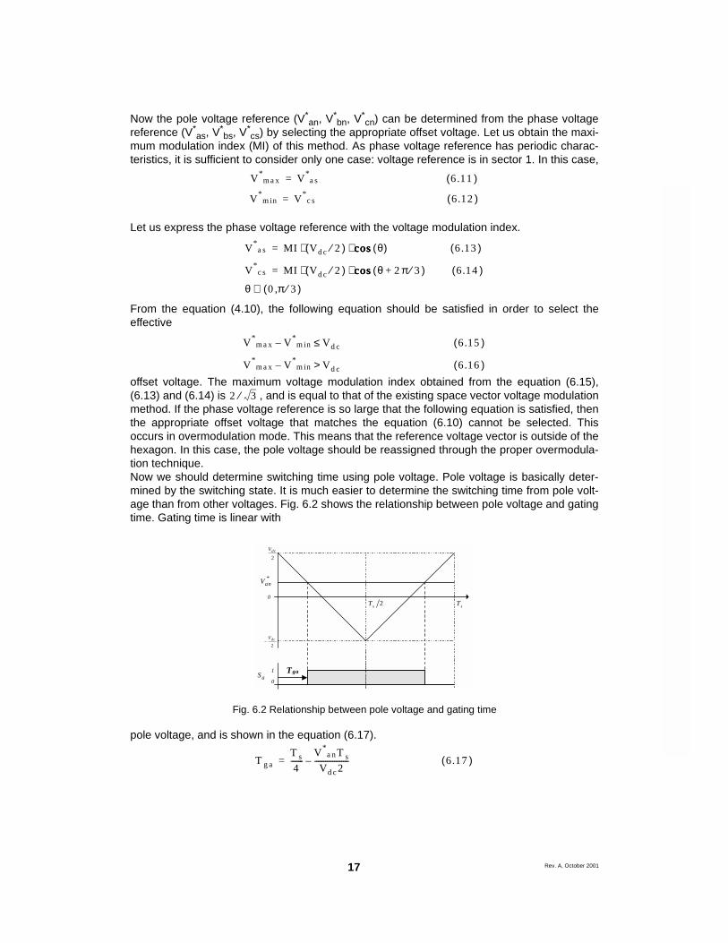
offset voltage. The maximum voltage modulation index obtained from the equation (6.15),(6.13) and (6.14) is , and is equal to that of the existing space vector voltage modulationmethod. If the phase voltage reference is so large that the following equation is satisfied, thenthe appropriate offset voltage that matches the equation (6.10) cannot be selected. Thisoccurs in overmodulation mode. This means that the reference voltage vector is outside of thehexagon. In this case, the pole voltage should be reassigned through the proper overmodula-tion technique.Now we should determine switching time using pole voltage. Pole voltage is basically deter-mined by the switching state. It is much easier to determine the switching time from pole volt-age than from other voltages. Fig. 6.2 shows the relationship between pole voltage and gatingtime. Gating time is linear with
Fig. 6.2 Relationship between pole voltage and gating time
pole voltage, and is shown in the equation (6.17).
V*max V
*as= 6.11( )
V*min V
*cs= 6.12( )
V*as MI Vdc 2⁄( ) θ( )coscoscoscos⋅ ⋅= 6.13( )
V*cs MI Vdc 2⁄( ) θ 2π 3⁄+( )coscoscoscos⋅ ⋅= 6.14( )
θ 0 π 3⁄,( )∈
V*max V
*min– Vdc≤ 6.15( )
V*max V
*min– Vdc> 6.16( )
2 3⁄
0
Vdc
2
−Vdc
2
0
Van*
Sa1 Tga
2sT sT
Tga
Ts
4-------
V*anTs
Vdc2-------------------–= 6.17( )

18
Rev. A, October 2001
After determining the offset voltage, the gating time can be calculated easily by substitutingthe pole voltage that is obtained by adding the offset voltage to the phase voltageVarious existing voltage modulation methods can be determined easily by using the offset volt-age expressed as V*
max, V*mid, V*
min). The principle of symmetric space vector voltage modu-lation is to locate the effective voltage vector (Vn,Vn+1) in the center of one modulation cycle.As shown in Fig. 6.2, this occurs when the absolute value of the maximum and minimum polevoltage are the same. Hence, the existing symmetric space vector voltage modulation can berealized by setting the offset voltage as a certain value that makes the maximum and minimumpole voltage have the same value.
So now, the offset voltage is as follows.
Fig. 6.3 shows the pole voltages that are the sum of phase voltage and offset voltage asshown in the equation (6.19).
Fig. 6.3 Pole voltage of SVPWM.h(a) MI = 0.3 (b) MI = 0.5 (c) MI = 0.7 (d) MI = 0.9
V*max Vsn+ V
*min Vsn+( )–= 6.18( )
VsnV
*max V
*min+
2--------------------------------------–= 6.19( )
0
Vdc
2
−Vdc
2 0 2πθ [rad]
(a ) (b )
(d )(c)
Van
V sn
Vas
Rev. A, October 200119
7. Real Implementation
An open-loop speed control system for a 3-phase AC induction motor using the V/Hz principle,and a speed controlled drive system for a 4 pole 3-phase BLDC motor is implemented using a3-phase voltage-controlled inverter. The outline of the control algorithm for each system isdescribed below.
IM• Obtain target frequency from ADC input.• Calculate output frequency.• Obtain output voltage magnitude.• Obtain output voltage phase, θ.• Calculate sinθ, cosθ.• Perform 2 phase/3 phase transformation• Load compare register with phase voltage corresponding timer value.
BLDC• Obtain speed reference from ADC input.• Calculate current speed from hall sensor signal.• Obtain reference voltage from speed error PI.• Load compare register with phase voltage corresponding timer value.
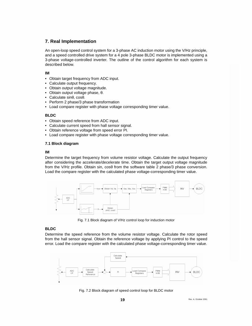
7.1 Block diagram
IMDetermine the target frequency from volume resistor voltage. Calculate the output frequencyafter considering the accelerate/decelerate time. Obtain the target output voltage magnitudefrom the V/Hz profile. Obtain sin, cosθ from the software table 2 phase/3 phase conversion.Load the compare register with the calculated phase voltage-corresponding timer value.
Fig. 7.1 Block diagram of V/Hz control loop for induction motor
BLDCDetermine the speed reference from the volume resistor voltage. Calculate the rotor speedfrom the hall sensor signal. Obtain the reference voltage by applying PI control to the speederror. Load the compare register with the calculated phase voltage-corresponding timer value.
Fig. 7.2 Block diagram of speed control loop for BLDC motor
ADCI/F
ObtainsinΘ, cosΘ
Obtain Vd, VqVout
Θ
Vas, Vbs, VcsPWMH/W INV
Load Compare Registers BLDC
Calculate Speed
Reference
ADCI/F
PILoad Compare
RegistersPWMH/W
INV BLDC
Calculate Speed
20
Rev. A, October 2001
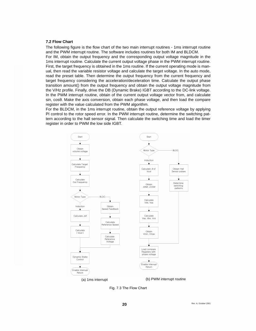
7.2 Flow ChartThe following figure is the flow chart of the two main interrupt routines - 1ms interrupt routineand the PWM interrupt routine. The software includes routines for both IM and BLDCM.For IM, obtain the output frequency and the corresponding output voltage magnitude in the1ms interrupt routine. Calculate the current output voltage phase in the PWM interrupt routine.First, the target frequency is obtained in the 1ms routine. If the current operating mode is man-ual, then read the variable resistor voltage and calculate the target voltage. In the auto mode,read the preset table. Then determine the output frequency from the current frequency andtarget frequency considering the acceleration/deceleration time. Calculate the output phasetransition amount() from the output frequency and obtain the output voltage magnitude fromthe V/Hz profile. Finally, drive the DB (Dynamic Brake) IGBT according to the DC-link voltage.In the PWM interrupt routine, obtain of the current output voltage vector from, and calculatesin, cosθ. Make the axis conversion, obtain each phase voltage, and then load the compareregister with the value calculated from the PWM algorithm.For the BLDCM, in the 1ms interrupt routine, obtain the output reference voltage by applyingPI control to the rotor speed error. In the PWM interrupt routine, determine the switching pat-tern according to the hall sensor signal. Then calculate the switching time and load the timerregister in order to PWM the low side IGBT.
Fig. 7.3 The Flow Chart
Start
Calculate θ of Vout
Motor Type
ObtainSINθ, COSθ
CalculateVds, Vqs
CalculateVas, Vbs, Vcs
ObtainVmin, Vmax
Enable interruptReturn
Obtain Hall Sensor pulses
Determine switching patterns
Induction
BLDC
Start
Obtainvolume voltage
Calculate Target Frequency
CalculateOut Frequency
Dynamic BrakeControl
Enable interruptReturn
ObtainSpeed Feedback
CalculateReference Speed
Calculate Reference
Voltage
CalculateVout
Calculate Δθ
Motor Type
Induction
BLDC
Load compare Registers with phase voltage
(a) 1ms interrupt (b) PWM interrupt routine

Rev. A, October 200121
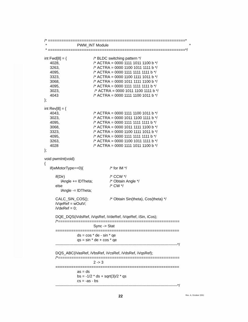
7.3 The Extract of the source codeThe main structure of the implemented software is shown below. A DSP of type TMS320F2406 is used.
/* =======================================================* * Main Module * * Main program initialization and Main loop execution * * =======================================================*/
void main()WORDi, j;
mainInit(); /* H/W Initialization */InitVar(); /* S/W Initialization */InitVFD(); /* VFD(Display) Initialization */EI;
while (1)
Keypad();VariUpdate();
void mainInit(void)
ioInit();Tmr1mInit();adc_init();da_init();SPIInit();
void adcInt(void)
ADCCTRL2 |= BIT_14; /* reset SEQ1 */EVAIFRA = BIT_1; /* eva1int flag reset */ADCCTRL2 |= BIT_9; /* clear INT_FLAG_SEQ1 */
22
Rev. A, October 2001
/* =============================================================* * PWM_INT Module * * =============================================================*/
int Fwd[8] = /* BLDC switching pattern */4028, /* ACTRA = 0000 1111 1011 1100 b */3263, /* ACTRA = 0000 1100 1011 1111 b */4095, /* ACTRA = 0000 1111 1111 1111 b */3323, /* ACTRA = 0000 1100 1111 1011 b */3068, /* ACTRA = 0000 1011 1111 1100 b */4095, /* ACTRA = 0000 1111 1111 1111 b */3023, /* ACTRA = 0000 1011 1100 1111 b */4043 /* ACTRA = 0000 1111 1100 1011 b */
;
int Rev[8] = 4043, /* ACTRA = 0000 1111 1100 1011 b */3023, /* ACTRA = 0000 1011 1100 1111 b */4095, /* ACTRA = 0000 1111 1111 1111 b */3068, /* ACTRA = 0000 1011 1111 1100 b */3323, /* ACTRA = 0000 1100 1111 1011 b */4095, /* ACTRA = 0000 1111 1111 1111 b */3263, /* ACTRA = 0000 1100 1011 1111 b */4028 /* ACTRA = 0000 1111 1011 1100 b */
;
void pwmInt(void)
if(wMotorType==0) /* for IM */
if(Dir) /* CCW */lAngle += lDTheta; /* Obtain Angle */
else /* CW */lAngle -= lDTheta;
CALC_SIN_COS(); /* Obtain Sin(theta), Cos(theta) */iVqeRef = wOutV;iVdeRef = 0;
DQE_DQS(iVdsRef, iVqsRef, iVdeRef, iVqeRef, iSin, iCos);/*======================================================
Sync -> Stat=======================================================
ds = cos * de - sin * qeqs = sin * de + cos * qe
-----------------------------------------------------------------------------------------------*/
DQS_ABC(iVasRef, iVbsRef, iVcsRef, iVdsRef, iVqsRef);/*======================================================
2 -> 3=======================================================
as = dsbs = -1/2 * ds + sqrt(3)/2 * qscs = -as - bs
-----------------------------------------------------------------------------------------------*/

Rev. A, October 200123
Max_MinABC(Max,Min,iVasRef,iVbsRef,iVcsRef);Offset = (Max+Min)>>1;
iVasRef -= Offset;iVbsRef -= Offset;iVcsRef -= Offset;
wPwmU = (wPwmAmp) + MulDiv((wPwmAmp),iVasRef,wBaseV);wPwmV = (wPwmAmp) + MulDiv((wPwmAmp),iVbsRef,wBaseV);wPwmW = (wPwmAmp) + MulDiv((wPwmAmp),iVcsRef,wBaseV);
CMPR1 = wPwmU; /* Load compare register */CMPR2 = wPwmV;CMPR3 = wPwmW;
else /* for BLDCM */Ha = (PADATDIR>>3 & 1);Hb = (PADATDIR>>4 & 1);Hc = (PADATDIR>>5 & 1);
Read_Speed(delT,Ha,Hb,Hc); /* for Speed Read */if(!flag.Run)
BuildTimer = 0;ACTRA = 0x0fff; /* All switch : forced high */
else
if(Dir) /* ---------------------------------- */ACTRA = Rev[((PADATDIR>>3))&7]; * | IOPA5 | IOPA4 | IOPA3 | */
Else * |--------------------------------| */ACTRA = Fwd[((PADATDIR>>3))&7]; * | Hc | Hb | Ha | */
* ---------------------------------- */wPwmU = wVOut4BLDC;
CMPR1 = wPwmU; /* Load compare register */CMPR2 = wPwmU;CMPR3 = wPwmU;
EVAIFRA = BIT_9; /* T1UFINT Flag Reset */
24
Rev. A, October 2001
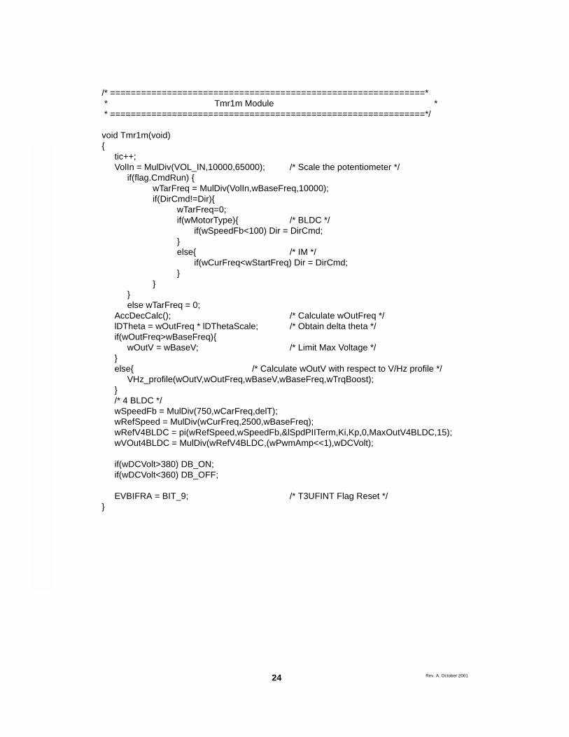
/* =============================================================* * Tmr1m Module * * =============================================================*/
void Tmr1m(void)
tic++;VolIn = MulDiv(VOL_IN,10000,65000); /* Scale the potentiometer */
if(flag.CmdRun) wTarFreq = MulDiv(VolIn,wBaseFreq,10000);if(DirCmd!=Dir)
wTarFreq=0;if(wMotorType) /* BLDC */
if(wSpeedFb<100) Dir = DirCmd;else /* IM */
if(wCurFreq<wStartFreq) Dir = DirCmd;
else wTarFreq = 0;
AccDecCalc(); /* Calculate wOutFreq */lDTheta = wOutFreq * lDThetaScale; /* Obtain delta theta */if(wOutFreq>wBaseFreq)
wOutV = wBaseV; /* Limit Max Voltage */else /* Calculate wOutV with respect to V/Hz profile */
VHz_profile(wOutV,wOutFreq,wBaseV,wBaseFreq,wTrqBoost);/* 4 BLDC */wSpeedFb = MulDiv(750,wCarFreq,delT);wRefSpeed = MulDiv(wCurFreq,2500,wBaseFreq);wRefV4BLDC = pi(wRefSpeed,wSpeedFb,&lSpdPIITerm,Ki,Kp,0,MaxOutV4BLDC,15);wVOut4BLDC = MulDiv(wRefV4BLDC,(wPwmAmp<<1),wDCVolt);
if(wDCVolt>380) DB_ON;if(wDCVolt<360) DB_OFF;
EVBIFRA = BIT_9; /* T3UFINT Flag Reset */

DISCLAIMER
FAIRCHILD SEMICONDUCTOR RESERVES THE RIGHT TO MAKE CHANGES WITHOUT FURTHERNOTICE TO ANY PRODUCTS HEREIN TO IMPROVE RELIABILITY, FUNCTION OR DESIGN. FAIRCHILDDOES NOT ASSUME ANY LIABILITY ARISING OUT OF THE APPLICATION OR USE OF ANY PRODUCTOR CIRCUIT DESCRIBED HEREIN; NEITHER DOES IT CONVEY ANY LICENSE UNDER ITS PATENTRIGHTS, NOR THE RIGHTS OF OTHERS.
TRADEMARKSThe following are registered and unregistered trademarks Fairchild Semiconductor owns or is authorized to use and isnot intended to be an exhaustive list of all such trademarks.
LIFE SUPPORT POLICY
FAIRCHILD’S PRODUCTS ARE NOT AUTHORIZED FOR USE AS CRITICAL COMPONENTS IN LIFE SUPPORTDEVICES OR SYSTEMS WITHOUT THE EXPRESS WRITTEN APPROVAL OF FAIRCHILD SEMICONDUCTOR CORPORATION.As used herein:1. Life support devices or systems are devices orsystems which, (a) are intended for surgical implant intothe body, or (b) support or sustain life, or (c) whosefailure to perform when properly used in accordancewith instructions for use provided in the labeling, can bereasonably expected to result in significant injury to theuser.
2. A critical component is any component of a lifesupport device or system whose failure to perform canbe reasonably expected to cause the failure of the lifesupport device or system, or to affect its safety oreffectiveness.
PRODUCT STATUS DEFINITIONS
Definition of Terms
Datasheet Identification Product Status Definition
Advance Information
Preliminary
No Identification Needed
Obsolete
This datasheet contains the design specifications forproduct development. Specifications may change inany manner without notice.
This datasheet contains preliminary data, andsupplementary data will be published at a later date.Fairchild Semiconductor reserves the right to makechanges at any time without notice in order to improvedesign.
This datasheet contains final specifications. FairchildSemiconductor reserves the right to make changes atany time without notice in order to improve design.
This datasheet contains specifications on a productthat has been discontinued by Fairchild semiconductor.The datasheet is printed for reference information only.
Formative orIn Design
First Production
Full Production
Not In Production
OPTOLOGIC™OPTOPLANAR™PACMAN™POP™Power247™PowerTrenchQFET™QS™QT Optoelectronics™Quiet Series™SILENT SWITCHER
FASTFASTr™FRFET™GlobalOptoisolator™GTO™HiSeC™ISOPLANAR™LittleFET™MicroFET™MicroPak™MICROWIRE™
Rev. H4
ACEx™Bottomless™CoolFET™CROSSVOLT™DenseTrench™DOME™EcoSPARK™E2CMOSTM
EnSignaTM
FACT™FACT Quiet Series™
SMART START™STAR*POWER™Stealth™SuperSOT™-3SuperSOT™-6SuperSOT™-8SyncFET™TinyLogic™TruTranslation™UHC™UltraFET
STAR*POWER is used under license
VCX™