an economics of nano technology: the relative importance of governmental funding and filing of...
TRANSCRIPT

8/10/2019 An Economics of Nano technology: The relative importance of Governmental funding and filing of patent applications
http://slidepdf.com/reader/full/an-economics-of-nano-technology-the-relative-importance-of-governmental-funding 1/21

8/10/2019 An Economics of Nano technology: The relative importance of Governmental funding and filing of patent applications
http://slidepdf.com/reader/full/an-economics-of-nano-technology-the-relative-importance-of-governmental-funding 2/21
Dr Debasis Patnaik Int. Journal of Engineering Research and Applications www.ijera.com ISSN : 2248-9622, Vol. 4, Issue 10( Part - 6), October 2014, pp.23-43
www.ijera.com 24 | P a g e
before in most other countries. ( )** denotes theactual budget recorded at the end of the respectivefiscal year. Estimations use the nanotechnology
definition as defined in NNI (Roco et al., 2000; thisdefinition does not include MEMS), and include the
publicly reported government spending.
Table 1. Worldwide government funding for nanotechnology R&D (June 2003)
Thus the United States has initiated amultidisciplinary strategy for development of scienceand engineering fundaments through the National
Nanotechnology Initiative announced in January2000. The vision-setting and collaborative model of
National Nanotechnology Initiative has receivedinternational acceptance. After 2001, virtually alldeveloped countries have national activities in thisarea. Japan and Western Europe have broad programs
backed by government, combining academic andindustry led R&D, and their current plans look aheadto four to five years. Other countries have encouragedtheir own areas of strength, several of them focusingon fields of the potential markets. For illustration,Korea has allocated about $10 million per year forthe next ten years in nanoelectronics memory chips(this is one of the projects summing about $200million per year in 2003 from government funding).Australia has identified nanoscale photonics as afocused area of government investment. Russia andUkraine maintain research activities establish in1990s, especially on advanced materials synthesisand processing. Emerging programs have beenannounced in Eastern Europe. In Asia Pacific, thereare growing programs in Japan, China, South Korea,Taiwan and Singapore. In North America, Canadian
National Research Council has created the NationalInstitute of Nanotechnology in Edmonton, Albertawith $80 million funding for five years. In Mexicothere are about 20 research groups, which areworking independently. Differences among countriesare observed in the research domain they are aimingfor, the level of program integration into variousindustrial sectors, and in the time scale of their R&Dtargets. Several countries (beginning with Japan,
Korea and China) have adopted coordinating officesat the national level similar to the National Scienceand Technology Council (NSTC) in the US.
Nanotechnology is growing in an environment whereinternational interactions accelerate in science,education and industrial R&D. A global strategy ofmutual interest is envisioned by connectingindividual programs of contributing countries,
professional communities, and internationalorganizations. International activities and agreementshave increased in importance. Examples are theagreements are between NSF (US) and EC (EU),
NSF (US) and Japan, APEC, Russia and China, thestates of New York (US) and Quebec (Canada). Forexample, NSF and EC have organized periodicalworkshops (four workshops are held in 2002 on:Manufacturing at the Nanoscale, RevolutionaryOpportunities of Nanotechnology and SocietalImplications, Tools for Measurements andManufacturing, and Materials) and sponsored a joint
program solicitation for proposals.The United States fiscal year 2004 funding requestfor nanoscale science, engineering and technology(noted in brief - nanotechnology) research anddevelopment (R&D) in ten federal departments andindependent agencies is summarized in Table 2(http://nano.gov). It emphasizes long-term,fundamental research aimed at discovering novel
phenomena, processes, and tools; addressing NNIGrand Challenges; supporting new interdisciplinarycenters and networks of excellence including shareduser facilities; supporting research infrastructure; andaddressing research and educational activities on thesocietal implications of advances in nanoscience andnanotechnology.

8/10/2019 An Economics of Nano technology: The relative importance of Governmental funding and filing of patent applications
http://slidepdf.com/reader/full/an-economics-of-nano-technology-the-relative-importance-of-governmental-funding 3/21
Dr Debasis Patnaik Int. Journal of Engineering Research and Applications www.ijera.com ISSN : 2248-9622, Vol. 4, Issue 10( Part - 6), October 2014, pp.23-43
www.ijera.com 25 | P a g e
Table 2 (6/2003). Contribution of key agencies to NNI
Nanoscale science and engineering R&D is mostly in a precompetitive phase (the major applications aretypically expected to come after five years and are not yet well defined), and there are good win-win partneringand effort-sharing opportunities. International collaboration in fundamental research, long-term technicalchallenges, metrology, education and studies on societal implications will play an important role in theaffirmation and growth of the field.
Some Figures about Nanotechnology R&D in Europe and BeyondA) Funding for nanotechnology R&D in Europe and worldwide

8/10/2019 An Economics of Nano technology: The relative importance of Governmental funding and filing of patent applications
http://slidepdf.com/reader/full/an-economics-of-nano-technology-the-relative-importance-of-governmental-funding 4/21
Dr Debasis Patnaik Int. Journal of Engineering Research and Applications www.ijera.com ISSN : 2248-9622, Vol. 4, Issue 10( Part - 6), October 2014, pp.23-43
www.ijera.com 26 | P a g e
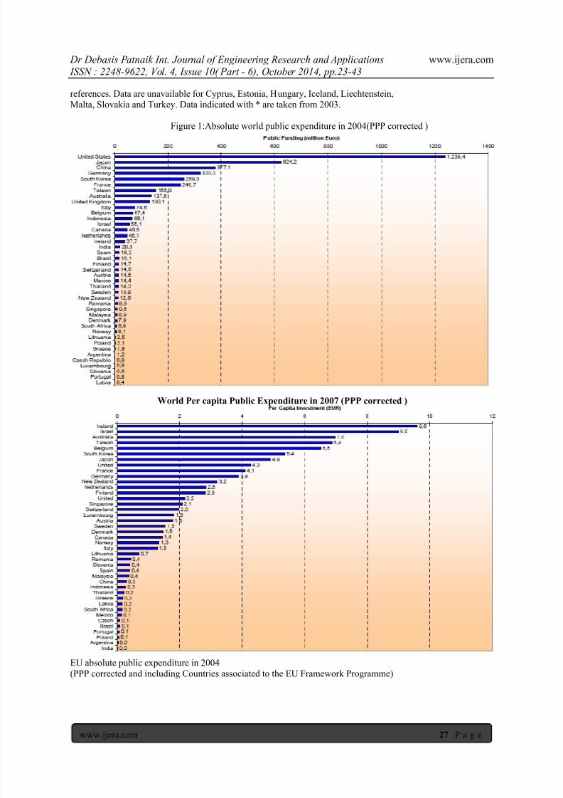
Table 1: Estimated worldwide public funding for nanotechnology R&D in 2004Source: European Commission, 2005 and various sources indicated by superscripted
8/10/2019 An Economics of Nano technology: The relative importance of Governmental funding and filing of patent applications
http://slidepdf.com/reader/full/an-economics-of-nano-technology-the-relative-importance-of-governmental-funding 5/21
8/10/2019 An Economics of Nano technology: The relative importance of Governmental funding and filing of patent applications
http://slidepdf.com/reader/full/an-economics-of-nano-technology-the-relative-importance-of-governmental-funding 6/21
Dr Debasis Patnaik Int. Journal of Engineering Research and Applications www.ijera.com ISSN : 2248-9622, Vol. 4, Issue 10( Part - 6), October 2014, pp.23-43
www.ijera.com 28 | P a g e
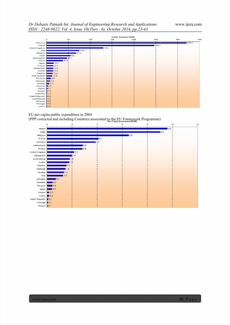
EU per capita public expenditure in 2004(PPP corrected and including Countries associated to the EU Framework Programme)
8/10/2019 An Economics of Nano technology: The relative importance of Governmental funding and filing of patent applications
http://slidepdf.com/reader/full/an-economics-of-nano-technology-the-relative-importance-of-governmental-funding 7/21
Dr Debasis Patnaik Int. Journal of Engineering Research and Applications www.ijera.com ISSN : 2248-9622, Vol. 4, Issue 10( Part - 6), October 2014, pp.23-43
www.ijera.com 29 | P a g e
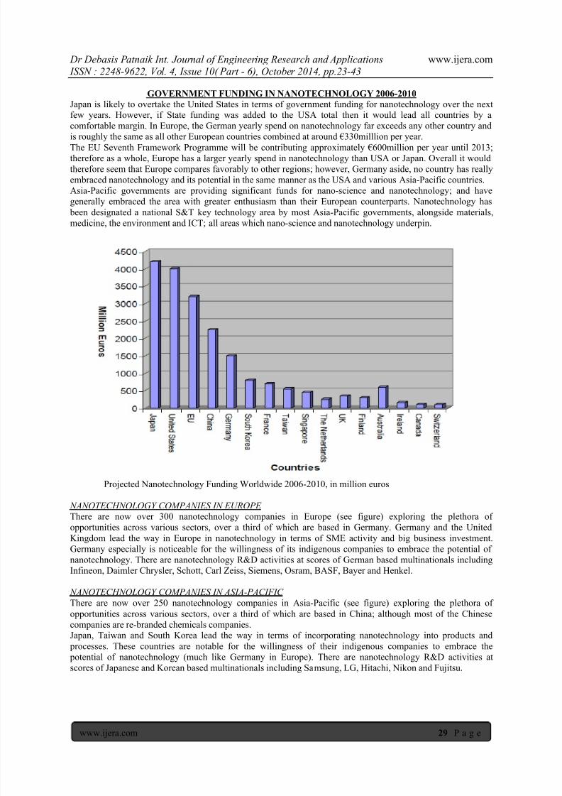
GOVERNMENT FUNDING IN NANOTECHNOLOGY 2006-2010Japan is likely to overtake the United States in terms of government funding for nanotechnology over the nextfew years. However, if State funding was added to the USA total then it would lead all countries by acomfortable margin. In Europe, the German yearly spend on nanotechnology far exceeds any other country and
is roughly the same as all other European countries combined at around €330milllion per year. The EU Seventh Framework Programme will be contributing appro ximately €600million per year until 2013;therefore as a whole, Europe has a larger yearly spend in nanotechnology than USA or Japan. Overall it wouldtherefore seem that Europe compares favorably to other regions; however, Germany aside, no country has reallyembraced nanotechnology and its potential in the same manner as the USA and various Asia-Pacific countries.Asia-Pacific governments are providing significant funds for nano-science and nanotechnology; and havegenerally embraced the area with greater enthusiasm than their European counterparts. Nanotechnology has
been designated a national S&T key technology area by most Asia-Pacific governments, alongside materials,medicine, the environment and ICT; all areas which nano-science and nanotechnology underpin.
Projected Nanotechnology Funding Worldwide 2006-2010, in million euros
NANOTECHNOLOGY COMPANIES IN EUROPEThere are now over 300 nanotechnology companies in Europe (see figure) exploring the plethora ofopportunities across various sectors, over a third of which are based in Germany. Germany and the UnitedKingdom lead the way in Europe in nanotechnology in terms of SME activity and big business investment.Germany especially is noticeable for the willingness of its indigenous companies to embrace the potential ofnanotechnology. There are nanotechnology R&D activities at scores of German based multinationals includingInfineon, Daimler Chrysler, Schott, Carl Zeiss, Siemens, Osram, BASF, Bayer and Henkel.
NANOTECHNOLOGY COMPANIES IN ASIA-PACIFICThere are now over 250 nanotechnology companies in Asia-Pacific (see figure) exploring the plethora ofopportunities across various sectors, over a third of which are based in China; although most of the Chinesecompanies are re-branded chemicals companies.Japan, Taiwan and South Korea lead the way in terms of incorporating nanotechnology into products and
processes. These countries are notable for the willingness of their indigenous companies to embrace the potential of nanotechnology (much like Germany in Europe). There are nanotechnology R&D activities atscores of Japanese and Korean based multinationals including Samsung, LG, Hitachi, Nikon and Fujitsu.

8/10/2019 An Economics of Nano technology: The relative importance of Governmental funding and filing of patent applications
http://slidepdf.com/reader/full/an-economics-of-nano-technology-the-relative-importance-of-governmental-funding 8/21
Dr Debasis Patnaik Int. Journal of Engineering Research and Applications www.ijera.com ISSN : 2248-9622, Vol. 4, Issue 10( Part - 6), October 2014, pp.23-43
www.ijera.com 30 | P a g e
Nanotechnology companies in Asia-Pacific 2007
Analysis method of patent applications for nano:
Data collection and pre-processing Nanotechnology publications from different countries’/ regions’ patent offices (re positories) were extractedfrom the esp@cenet ‘‘worldwide’’ database into our database by using keyword ‘‘title–abstract’’ searching.
A patent office is a governmental or intergovernmental organization which controls the issue of patents.Different countries have their own patent offices, such as the USPTO, the JPO, the Canadian IntellectualProperty Office (CIPO), and the South Korean Intellectual Property Office (KIPO). In addition to national(country level) patent offices, there are several regional (country group level) patent offices as well, such as theEPO and the World Intellectual Property Organization (WIPO). The EPO grants European patents for the 27member states of the European Patent Convention. The WIPO is a specialized agency of the United Nationswith 184 member states in 2008. It grants patents for all of its member states. Many countries publish patentapplications and/ or grant patent rights for public information (Chemical Abstracts Service 2008).
A reliable international database covering patent information from multiple patent offices is the esp@ cenet‘‘worldwide’’ database, which is maintained by the EPO together with the member states of the European PatentOrganization. Esp@cenet includes three databases:
– ‘‘EPO’’ database – ‘‘WIPO’’ database – ‘‘worldwide’’ database The esp@cenet ‘‘worldwide’’ database contains the patent applications examined and published by 85individual countries’/regions’ patent offices, including the USPTO, EPO, and JPO. The esp@cenet‘‘worldwide’’ database holds more than 60 million patents (Espacenet Website, ‘‘Coverage of the worldwidedatabase’’) (Espacenet Website, ‘‘Coverage of the worldwide database’’) (EPO 2008). English translations forall other languages are provided for the bibliographic information, and selected content information (such asabstract, claim, and description) are also provided. Owing to the limitation of the search functions of esp@cenet,we collected the patent applications by searching the nanotechnology keywords only in each patent application’s
title and abstract (‘‘title–abstract’’ search). The esp@cenet ‘‘worldwide’’ database previously has been used to examine patents in biology (Oldham andCutter 2006), hydrogen and fuel cells (Seymour et al. 2007), and globalization of knowledge (Andersen et al.2006).
Patent parsingTwo sets of patent information were parsed into our database from the collected patent applications:
– Nanotechnology patent applications published in different countries’/regions’ patent offices (repositories) – Patent family information of these patent applications.Table 1 shows the data field limitation of our patent application collection. Most of the data fields are availablein the esp@cenet ‘‘worldwide’’ database.

8/10/2019 An Economics of Nano technology: The relative importance of Governmental funding and filing of patent applications
http://slidepdf.com/reader/full/an-economics-of-nano-technology-the-relative-importance-of-governmental-funding 9/21
Dr Debasis Patnaik Int. Journal of Engineering Research and Applications www.ijera.com ISSN : 2248-9622, Vol. 4, Issue 10( Part - 6), October 2014, pp.23-43
www.ijera.com 31 | P a g e
However, it does not contain the citation information for patent applications published in patent offices otherthan EPO and WIPO (Espacenet Website, ‘‘What is a cited document?’’). For some regional or country patentoffices, the bibliographic data (such as the application country, European patent classification code (EPC),claim, or description) are incomplete. All the selected repositories in our study are part of EPO and WIPO.A patent application for an invention is originally filed in one country; however, it can be filed later in othercountries as well. The original, first application filing generally is considered to be the priority application(Hingley and Park 2003). In esp@cenet, such related applications or ‘‘members of corresponding documents’’or ‘‘equivalents’’ and have exactly the same priority (Espacenet Website, ‘‘Also published as documents’’). A patent family is a group of patents that are all related to each other. We use the esp@cenet patent ‘‘simplefamily’’ definition as comprising all the documents having exactly the same priority or combination of priorities(Espacenet Website, ‘‘Patent families’’). The International Patent Documentation Centre (INPADOC) defines as‘‘expanded family’’ all the documents sharing directly or indirectly (e.g., via a third docu ment) at least one
priority (Espacenet Website, ‘‘Patent families’’).
IV. ResultsWe collected the nanotechnology patent applications published from 1991 to 2008 from the esp@cenet‘‘worldwide’’ database. We focused attention on the leading 15 country/regiona l patent offices that cover morethan 98% of the whole collection; each has more than 100 patent applications.
Global increase of nanotechnology patents
The evolution of the total number of nanotechnology patent applications in the 15 repositories per year from1991 to 2008 is shown in Fig 1. This figure also shows the number of non-overlapping nanotechnology patentapplications by considering one patent application per family. The annual rate of increase for all the patent
publications is more pronounced between 2000 and 2008 (34.5%). This rate is higher than that of ScienceCitation Index’s article publication rate of 20–25% for the same period when we use the same keyword ‘‘title– abstract’’ search approach as for patent applications. The percentage of nanotechnology patent application as compared to the total number of patent applications inall the technical areas is illustrated in Fig. 2.

8/10/2019 An Economics of Nano technology: The relative importance of Governmental funding and filing of patent applications
http://slidepdf.com/reader/full/an-economics-of-nano-technology-the-relative-importance-of-governmental-funding 10/21
Dr Debasis Patnaik Int. Journal of Engineering Research and Applications www.ijera.com ISSN : 2248-9622, Vol. 4, Issue 10( Part - 6), October 2014, pp.23-43
www.ijera.com 32 | P a g e
Fig. 1 Longitudinal evolution of the total number of nanotechnology patent applications in the 15 repositories per year (‘‘title abstract,’’ 1991– 2008)
Fig. 2 Longitudinal evolution of the percentage of patent publications on nanotechnology versus all topics, inthe repositories of leading 15 countries/regions and USA from 1991 to 2008 using keyword ‘‘title– abst ract’’search
The nanotechnology patent application percentages for the USPTO reported in the above figure are consistentwith the data trends reported in previous studies (Huang et al. 2006; Hu et al. 2007) where the granted patentswere searched by ‘‘ti tle –claims’’ from 1991 to 2004. In that study, the percentage of granted patents reached1.09% in 2004 versus 0.63% for patent applications in Fig. 2. Our previous studies also showed that thenanotechnology- granted patent percentages for ‘‘full -text’’ sea rch was 4.85% in 2004 for the USPTO.
Number of patent applications per repository
Table 2 lists the numbers of nanotechnology patent applications published by each of the 15 countries/ regions’ patent offices from 1991 to 2008. The USPTO examined and published the largest number of nanotechnology patent applications, followed by the patent offices of the PRC and Japan.

8/10/2019 An Economics of Nano technology: The relative importance of Governmental funding and filing of patent applications
http://slidepdf.com/reader/full/an-economics-of-nano-technology-the-relative-importance-of-governmental-funding 11/21
Dr Debasis Patnaik Int. Journal of Engineering Research and Applications www.ijera.com ISSN : 2248-9622, Vol. 4, Issue 10( Part - 6), October 2014, pp.23-43
www.ijera.com 33 | P a g e
Table 2 Nanotechnology patent applications published in the top 15 countries/regions’ patent offices in theinterval 1991 to 2008 using k eyword ‘‘title–abstract’’ search The total number of nanotechnology patent applications published from 1991 to 2008 by authors from the USand PRC are estimated each at over 17,000. Over 20% of the US patent applications and 4% of the PRC’s are inforeign repositories.Figures 3 and 4 show the evolution of the numbers of nanotechnology patent applications published in differentcountries’/regions’ patent offices by year. Since the patent offices of the US, PRC, Japan, and South Korea hadmany more nanotechnology patent applications, we present their evolution trends in Fig. 3. The evolution trendsof the other 11 countries’/ regions’ patent offices are shown in Fig. 4. The patent offices of the US, PRC, Japan, and South Korea have significantly more nanotechnology patentapplications than other patent offices, and all experienced larger increases especially after 2003. The PRC’srepository surpassed the USA’ repository after 2006. As shown in Fig. 4, the other 11 patent offices haveexperienced mostly increases but also decreased in recent years. The patent offices of the Russian Federation,
Brazil, and the United Kingdom (UK) reached their peaks in 2008 with 162, 103, and 68 nanotechnology patentapplications, respectively. The Ukraine’s patent office peaked in 2007 with 87 nanotechnology patentapplications, and the patent offices of Germany and New Zealand reached their peaks in 2006 with 164 and 21nanotechnology patent applications, respectively. Canada’s and Mexico’s patent offices reached their peaks in 2005 with 274 and 94 nanotechnology patent applications, respectively. Australia’s and France’s patent offices
peaked in 2003 with 343 and 57 nanotechnology patent applications, respectively. Taiwan’s patent office hadmore than 200 nanotechnology patent applications per year from 2004 to 2007 with 2006 as the peak (343applications); however, the number dropped dramatically in 2008 to only three nanotechnology patentapplications probably due to a delay in collecting the 2008 Taiwan patent data by the esp @cenet ‘‘worldwide’’database. In all following analyses, we used 2007 data for Taiwan’s patent office instead of 2008.
Fig. 3 The numbers of nanotechnology patent applications from all countries in the patent offices of the US,PRC, Japan, and South Kor ea using ‘‘title–abstract’’ search, from 1991 to 2008

8/10/2019 An Economics of Nano technology: The relative importance of Governmental funding and filing of patent applications
http://slidepdf.com/reader/full/an-economics-of-nano-technology-the-relative-importance-of-governmental-funding 12/21
Dr Debasis Patnaik Int. Journal of Engineering Research and Applications www.ijera.com ISSN : 2248-9622, Vol. 4, Issue 10( Part - 6), October 2014, pp.23-43
www.ijera.com 34 | P a g e
Fig. 4 The numbers of nanotechnology patent applications from all the countries in the remaining 11 patentoffices using ‘‘title–abstract’’ search from 1991 to 2008. Most patent offices generally publish the country of origin of the patent publications, with the exceptions ofJapan, Australia, and New Zealand. Table 3 lists the top five countries where patent applications were filledfrom 1991 to 2008. For several of the other patent offices, a small portion of their patent applications may haveincomplete applicant country information. In these cases, we manually verified the information. For eachapplication having the applicant same as the inventor(s), we then used the country of the first inventor as itsapplicant country. As a comparison, we also list the numbers of nanotechnology patent applications published in2000 (the year before the establishment of the US National Nanotechnology Initiative; Roco et al. 2000) and2008 (the most recent year with data available for the whole year).The USA was the most active internationally with the largest numbers of nanotechnology patent applicants
published in other patent offices. It ranked first in three out of the 12 patent offices, including its own patentoffice, Canada’s, and Mexico’s patent offices; it ranked second in the patent offices of six other countries; andthird in the remaining three patent offices. Japan, Germany, South Korea, and France are the most activeinternationally after the USA.These results on country ranking generally are consistent with those reported in the previous study on granted
patents at USPTO using ‘‘title–claims’’ search (Li et al. 2007), in which study the top five applicant countries ofUSPTO nanotechnology-granted patents published from 1976 to 2004 were the US (3,450 patents), Japan (517
patents), Germany (204 patents), France (156 patents), and South Korea (131 patents), with Taiwan being theseventh. In this study, the top five applicant countries identified were the US, Japan, South Korea, Germany, andTaiwan. However, the numbers of nanotechnology patent documents reported in this study are different fromthose reported by Li et al. (2007) due to three reasons. First, instead of using the granted patents as used by Li etal. (2007), we used the published patent applications as the data source in this study, because the esp@cenet‘‘worldwide’’ database does not differentiate granted patents from published patent applications. Second, in this study involving 15 reposit ories we could not use the more complete ‘‘title/abstract/claims’’ used in previousstudy only for the USPTO. Third, our results are based on the data published from 1991 to 2008 while thenumbers reported by Li et al. (2007) are based on the data published from 1976 to 2004. Many patent officeshave published a large number of nanotechnology patents in recent years.Table 3 shows that all the patent offices except those of Canada and Mexico had the largest numbers ofnanotechnology patent applications publ ished by applicants from their own countries. This indicates a ‘‘homeadvantage’’ effect. As defined in previous studies, the ‘‘home advantage’’ effect is the tendency of domesticapplicants to file more patents with their home country patent office than foreign applicants (EuropeanCommission 1997; Ganguli 1998; Criscuolo 2005).By comparing the numbers of nanotechnology patent applications published in 2000 and 2008, the tremendousincrease in nanotechnology patent applications from each top applicant country can be easily perceived.Especially notable are the increases recorded by Mexico, Brazil, and Ukraine.

8/10/2019 An Economics of Nano technology: The relative importance of Governmental funding and filing of patent applications
http://slidepdf.com/reader/full/an-economics-of-nano-technology-the-relative-importance-of-governmental-funding 13/21
Dr Debasis Patnaik Int. Journal of Engineering Research and Applications www.ijera.com ISSN : 2248-9622, Vol. 4, Issue 10( Part - 6), October 2014, pp.23-43
www.ijera.com 35 | P a g e
8/10/2019 An Economics of Nano technology: The relative importance of Governmental funding and filing of patent applications
http://slidepdf.com/reader/full/an-economics-of-nano-technology-the-relative-importance-of-governmental-funding 14/21
Dr Debasis Patnaik Int. Journal of Engineering Research and Applications www.ijera.com ISSN : 2248-9622, Vol. 4, Issue 10( Part - 6), October 2014, pp.23-43
www.ijera.com 36 | P a g e
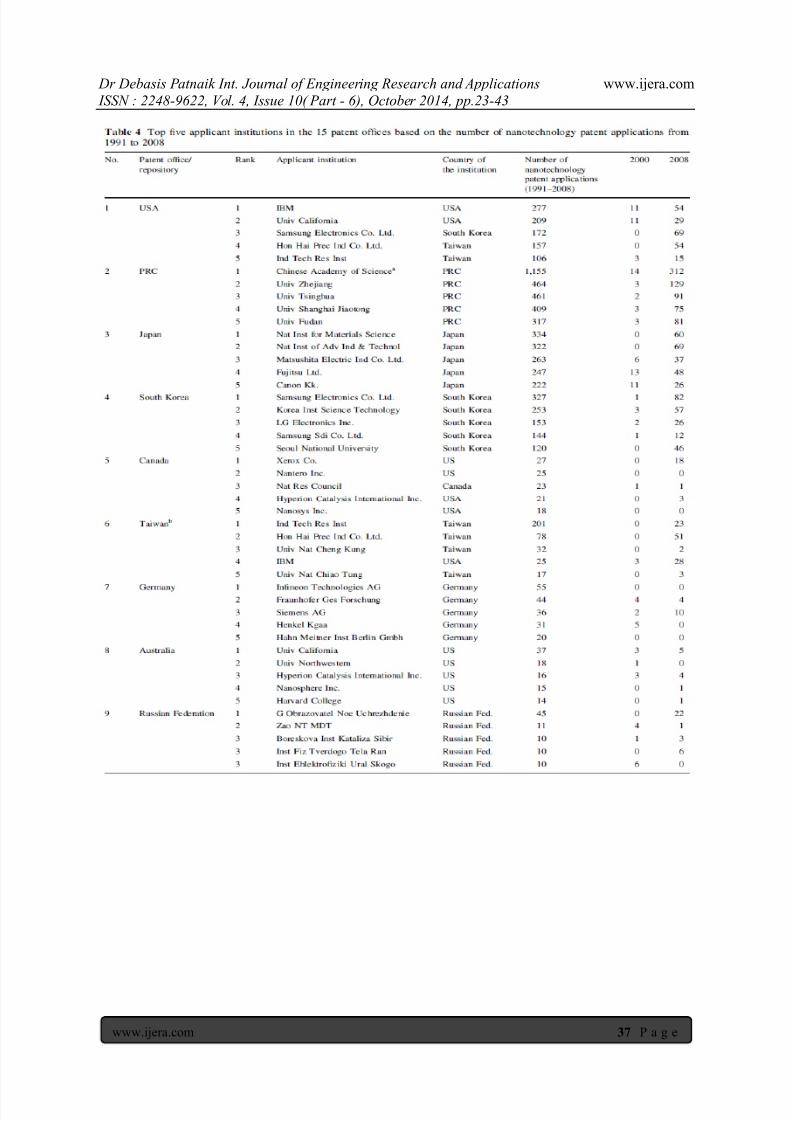
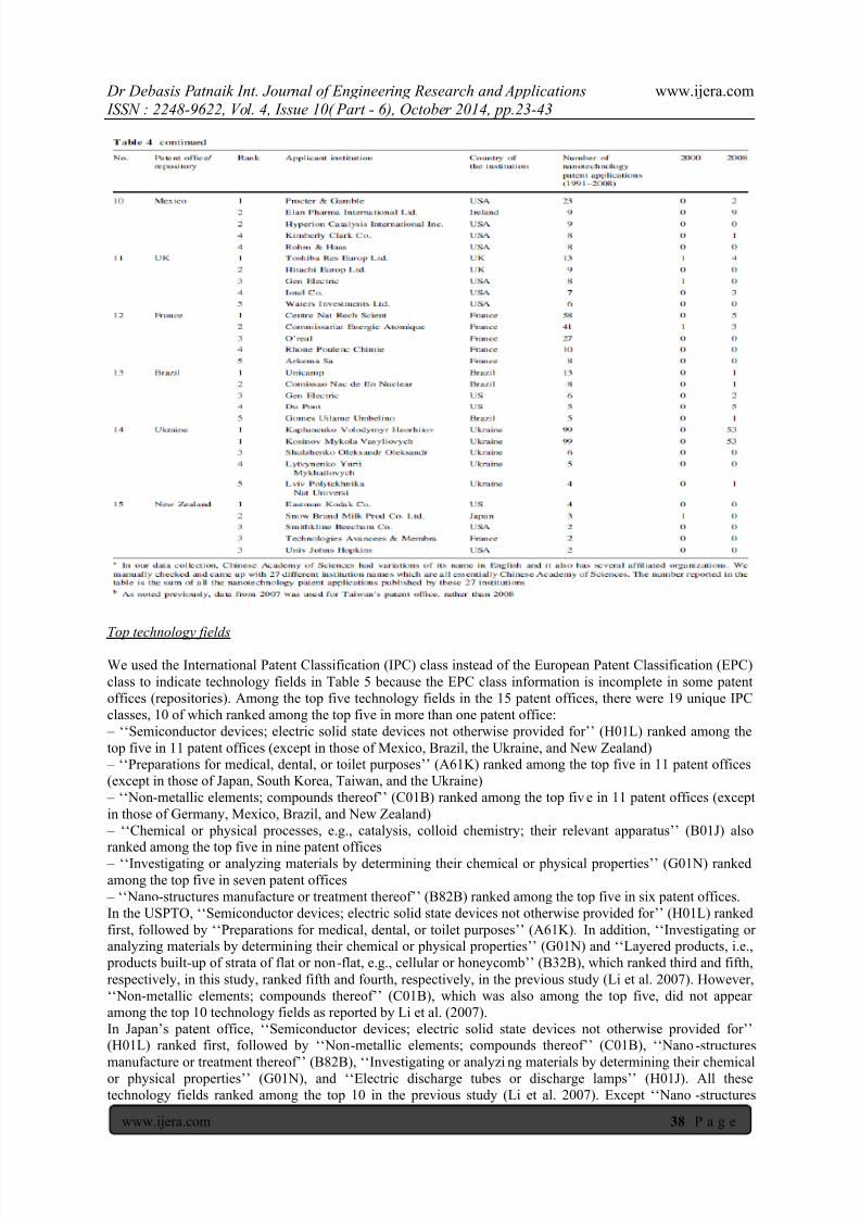
Top applicant institutions
Table 4 lists the leading five applicant institutions per repository that includes large companies, universities, andresearch centers. In each of the patent offices of the PRC, South Korea, Germany, Russian Federation, France,and Ukraine, all of the top five applicant institutions were from the home country. In contrast, all the top fiveapplicant institutions in Australia’s patent office came from the USA. Four out of the top five applicationinstitutions in both Canada’s and Mexico’s patent offices were from the USA. In addition, none of the top fiveapplicant institutions in New Zealand’s patent office was from its home country. Some internationally active
applicant institutions that ranked among the top five in different countries’/regions’ patent offi ces included IBM(from the US), the University of California (from the USA), Samsung Electronics Co. Ltd. (South Korea), HonHai Prec Ind Co. Ltd. (Taiwan), Industrial Technology Research Institute (Ind Tech Res Inst; Taiwan), HyperionCatalysis International Inc. (USA), and General Electric (USA).
In the USA’s patent office, IBM ranked first, followed by the University of California and Samsung ElectronicCo. In Japan’s patent office, the National Institute for Materials Science (Nat Inst for Materials Sc ience) rankedfirst followed by the National Institute of Advanced Industrial Science and Technology (Nat Inst of Adv Ind &Technol) and Matsushita Electric Ind Co. Ltd. In PRC’s patent offices, all the leading applicants are academic oracademy research institutions.
Compared with 2000, there is a general increase in the number of nanotechnology patent applications published by the top institutions in 2008. Among the top five institutions, in each of the patent offices of the USA, PRC,and Australia, the institution with the largest numbers of nanotechnology patent applications from 1991 to 2008also ranked first in 2000.
8/10/2019 An Economics of Nano technology: The relative importance of Governmental funding and filing of patent applications
http://slidepdf.com/reader/full/an-economics-of-nano-technology-the-relative-importance-of-governmental-funding 15/21
Dr Debasis Patnaik Int. Journal of Engineering Research and Applications www.ijera.com ISSN : 2248-9622, Vol. 4, Issue 10( Part - 6), October 2014, pp.23-43
www.ijera.com 37 | P a g e
8/10/2019 An Economics of Nano technology: The relative importance of Governmental funding and filing of patent applications
http://slidepdf.com/reader/full/an-economics-of-nano-technology-the-relative-importance-of-governmental-funding 16/21
8/10/2019 An Economics of Nano technology: The relative importance of Governmental funding and filing of patent applications
http://slidepdf.com/reader/full/an-economics-of-nano-technology-the-relative-importance-of-governmental-funding 17/21
Dr Debasis Patnaik Int. Journal of Engineering Research and Applications www.ijera.com ISSN : 2248-9622, Vol. 4, Issue 10( Part - 6), October 2014, pp.23-43
www.ijera.com 39 | P a g e
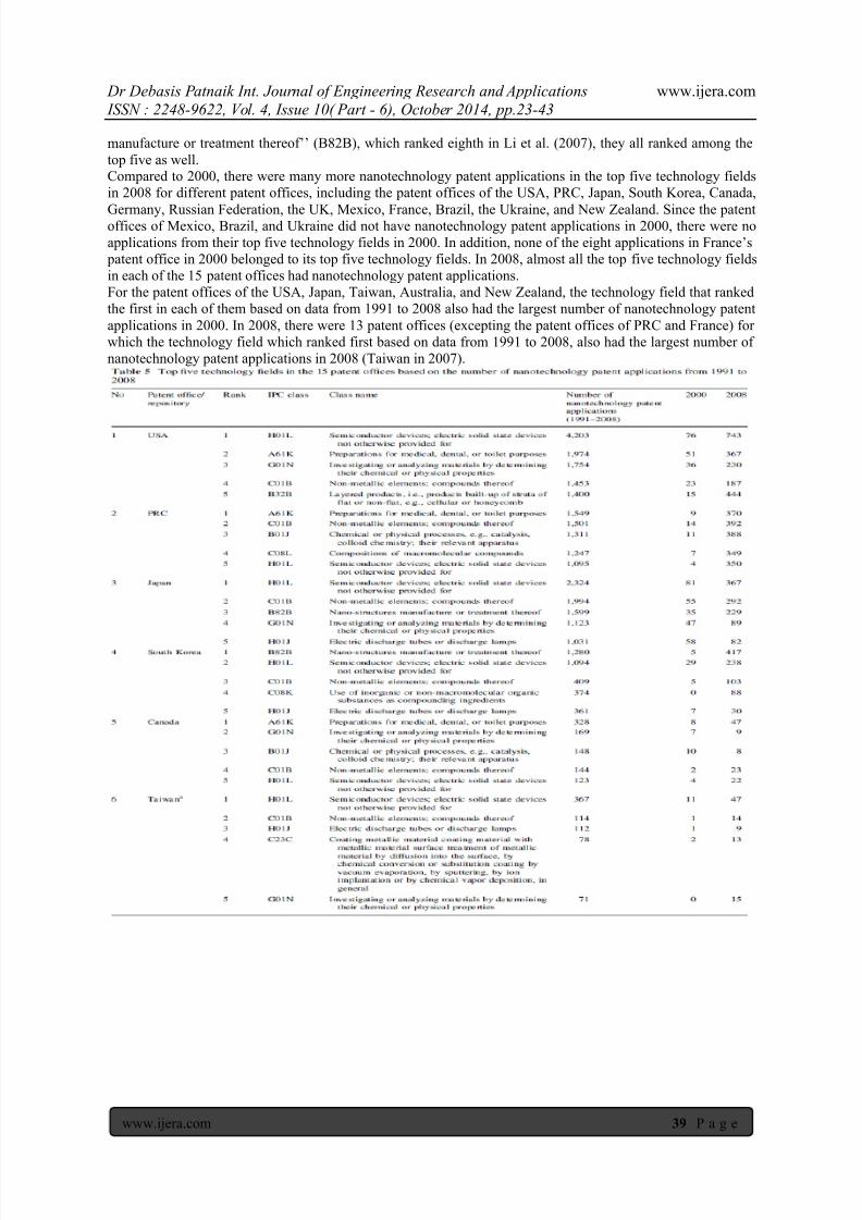
manufacture or treatment thereof’’ (B82B), which ranked eighth in Li et al. (2007), they all ranked among thetop five as well.Compared to 2000, there were many more nanotechnology patent applications in the top five technology fieldsin 2008 for different patent offices, including the patent offices of the USA, PRC, Japan, South Korea, Canada,
Germany, Russian Federation, the UK, Mexico, France, Brazil, the Ukraine, and New Zealand. Since the patentoffices of Mexico, Brazil, and Ukraine did not have nanotechnology patent applications in 2000, there were noapplications from their top five technology fields in 2000. In addition, none of the eight applications in France’s
patent office in 2000 belonged to its top five technology fields. In 2008, almost all the top five technology fieldsin each of the 15 patent offices had nanotechnology patent applications.For the patent offices of the USA, Japan, Taiwan, Australia, and New Zealand, the technology field that rankedthe first in each of them based on data from 1991 to 2008 also had the largest number of nanotechnology patentapplications in 2000. In 2008, there were 13 patent offices (excepting the patent offices of PRC and France) forwhich the technology field which ranked first based on data from 1991 to 2008, also had the largest number ofnanotechnology patent applications in 2008 (Taiwan in 2007).

8/10/2019 An Economics of Nano technology: The relative importance of Governmental funding and filing of patent applications
http://slidepdf.com/reader/full/an-economics-of-nano-technology-the-relative-importance-of-governmental-funding 18/21
Dr Debasis Patnaik Int. Journal of Engineering Research and Applications www.ijera.com ISSN : 2248-9622, Vol. 4, Issue 10( Part - 6), October 2014, pp.23-43
www.ijera.com 40 | P a g e

8/10/2019 An Economics of Nano technology: The relative importance of Governmental funding and filing of patent applications
http://slidepdf.com/reader/full/an-economics-of-nano-technology-the-relative-importance-of-governmental-funding 19/21
Dr Debasis Patnaik Int. Journal of Engineering Research and Applications www.ijera.com ISSN : 2248-9622, Vol. 4, Issue 10( Part - 6), October 2014, pp.23-43
www.ijera.com 41 | P a g e
Patent family analysis within each patent office
Table 6 lists the numbers of nanotechnology patent applications published in single patent office, two or more patent offices, and three or more patent offices. For example, 2,939 patent applications that were published inthe US patent office had been also published in at least one other patent office. Among those patent applications,741 had been publ ished in three or more countries’/regions’ patent offices. The patent offices of Japan, the PRC,and South Korea also had relatively larger numbers of nanotechnology patent applications published in multiple
patent offices.For each patent office, we also identified other patent offices with which it shared the greatest numbers ofnanotechnology patent applications for the interval between 1991 and 2008. For example,
– The top five patent offices sharing nanotechnology patent applications with the USPTO were Japan (1,258),PRC (725); South Korea (636), Taiwan (353), and Canada (350). Our analysis shows that all other patent offices(except for Brazil’s patent offices) shared the largest numbers of nanotechnology patent applications with the USPTO.
– The top five patent offices sharing nanotechnology patent applications with the PRC repository were those ofthe USA (725), South Korea (624), Japan (416), Taiwan (68), and Canada (40).
– The top five patent offices sharing nanotechnology patent applications with the JPO were those of the USA(1258), South Korea (450), PRC (416), Taiwan (107), and Canada (106).

8/10/2019 An Economics of Nano technology: The relative importance of Governmental funding and filing of patent applications
http://slidepdf.com/reader/full/an-economics-of-nano-technology-the-relative-importance-of-governmental-funding 20/21
Dr Debasis Patnaik Int. Journal of Engineering Research and Applications www.ijera.com ISSN : 2248-9622, Vol. 4, Issue 10( Part - 6), October 2014, pp.23-43
www.ijera.com 42 | P a g e
V. ConclusionsKey findings from the longitudinal analysis of nanotechnology patent applications between 1991 and 2008
are:• The worldwide growth rate of the number of nanotechnology patent applications between 2000 and 2008 is
about 34.5% (Fig. 1). This rate is larger than the corresponding rate of increase for International Citation Indexarticles of about 25%. The baseline growth rates of the number of patent applications for continuing topics are16.14 and 12.57 times in the interval from 1991 to 2008 for the USPTO and the top 15 nanotechnology patentrepositories, respectively. The new nanotechnology topics in 2008 as compared with 2000 represent 92% in theUSA and 68% for top 15 repositories. The baseline growth rate is significant in the PRC patent office, but thedata available in 2000 are too limited to generate a content map in that year for comparison with 2008. Thelargest number of nanotechnology patent applications, as well as of the patent application families, are at the
patent offices of the USA, PRC, Japan, and South Korea.• A higher number of nanotechnology patent applications are published by applicants from their owncountries/regions, indicating significant ‘‘home advantage’’ effects. The USA, Japan, Germany, South Korea,and France were the largest contributors in patent offices other than its repository. The top 15 patent officesexcept for Brazil’s patent office shared the largest numbers of nanotechnology patent applications with theUSPTO. Japan is the USPTO’s largest partner cosharing 1,258 nanotechnology patent applications.
• Applicant institutions with large international activity are illustrated by IBM (from the USA), the University ofCalifornia (from the USA), Samsung Electronics Co. Ltd. (from South Korea), Hon Hai Prec Ind Co. Ltd. (fromTaiwan), and Industrial Technology Research Institute (Ind Tech Res Inst; from Taiwan), Hyperion CatalysisInternational Inc. (from the USA), and General Electric (Gen Electric, from the USA).• The ranking of the most productive institutions and the categories of the lead technology fie lds in patentrepositories have had relatively small changes over time, and few institutions or categories of technology fieldswere able to break into the top ranks. However, specific topics within various technology field categorieschanged rapidly after 2000. Topics that increased in 2008 in most of the 15 patent offices included: ‘‘Compositematerials,’’ ‘‘Deionized water,’’ ‘‘Gate electrodes,’’ ‘‘High purities,’’ ‘‘Metal nanoparticles,’’ ‘‘Organicsolvents,’’ ‘‘Particle diameters,’’ ‘‘PH values,’’ ‘‘Quantum dots,’’ and ‘‘Semiconductor Devices.’’ • Several top technology fields (represented by IPC class) were shared by multiple repositories. ‘‘Semiconductordevices; electric solid state devices not otherwise provided for’’ (H01L) was among the top five t echnologyfields in 11 out of the 15 patent offices. The following fields ranked among the top five in multiple repositories:
‘‘Preparations for medical, dental, or toilet purposes’’ (A61K), ‘‘Non -metallic elements; compounds thereof’’(C01B), ‘‘Chemical or physical processes, e.g., catalysis, colloid chemistry; their relevant apparatus’’ (B01J),‘‘Investigating or analyzing materials by determining their chemical or physical properties’’ (G01N), and‘‘Nano -structures manufacture or treatment thereof’’ (B82 B).
REFERENCES [1.] NSTC, 2000, "Nanostructure Science and Technology", Chapter 8: Research Programs on
Nanotechnology in the World, pp. 131-150.[2.] M.C. Roco, 2001, " International Strategy for Nanotechnology Research and Development", Journal of
Nanoparticle Research, Kluwer Academic Publ., Vol. 3, No. 5-6, pp. 353-360.[3.] M.C. Roco and W.S. Bainbridge, eds., 2001, "Societal Implications of Nanoscience and
Nanotechnology", Kluwer Academic Publishers, Boston, pp. 3-4.[4.] Survey of EU Member States R&D funding for nanotechnology carried out in the Council of the
European Union (response from Austria).[5.] Survey of EU Member States R&D funding for nanotechnology carried out in the Council of the
European Union (response from Belgium).[6.] Australian Nanotechnology: Capability and Commercial Potential , Invest Australia Report (2005)
http://www.investaustralia.gov.au/[7.] Survey of EU Member States R&D funding for nanotechnology carried out in the Council of the
European Union (response from Denmark).[8.] Final Report of the International Dialogue on Responsible Research and Development of
Nanotechnology , Questionnaire Responses and Background Information (2004)http://www.nanoandthepoor.org/Attachment_F_Responses_and_Background_Info_040 812.pdf
[9.] Survey of EU Member States R&D funding for nanotechnology carried out in the Council of theEuropean Union (response from Finland).
[10.] India, China front-runners in nanotech research, A. Vaidya, The Times of India, January 24 2005http://timesofindia.indiatimes.com/articleshow/999932.cms .
8/10/2019 An Economics of Nano technology: The relative importance of Governmental funding and filing of patent applications
http://slidepdf.com/reader/full/an-economics-of-nano-technology-the-relative-importance-of-governmental-funding 21/21
Dr Debasis Patnaik Int. Journal of Engineering Research and Applications www.ijera.com ISSN : 2248-9622, Vol. 4, Issue 10( Part - 6), October 2014, pp.23-43
www.ijera.com 43 | P a g e
[11.] Presentation of Training Initiatives within Asia-Pacific Programmes , L. Liu, Nanotechnology ResearchInstitute (AIST), Japan, Workshop on Research Training in Nanosciences and Nanotechnologies:Current Status and Future Needs, April 2005, Brussels Irish Council for Science, Technology &
Innovation Statement on Nanotechnology , July 2004
[12.] Presentation of Training Initiatives within Asia-Pacific Programmes , L. Liu, Nanotechnology ResearchInstitute (AIST), Japan, Workshop on Research Training in Nanosciences and Nanotechnologies:Current Status and Future Needs, April 2005, Brussels
[13.] Nanotechnology in Asia 2003, Asian Technology Information Programme (AITP) April 2003[14.] Nanotechnology and the Poor: Opportunities and Risks , Meridian Institute, January 2005[15.] Nanotech business entering Singapore too (report on a presentation of H-G Lee of LG Electronics), L.
Liu, Asia Pacific Nanotech Weekly (2004/11/ 2 #40)[16.] Response to questionnaire on nanotechnology (for the Royal Society and Royal Academy of
Engineering study on nanotechnology), A. Pacholak, British Embassy Warsaw (2003)[17.] European Commission, Towards a European Strategy for Nanotechnology , COM(2004) 338.[18.] Albert R, Barabasi AL (2002) Statistical mechanics of complex networks. Rev Mod Phys 74:47 – 97[19.] Andersen PH, Drejer I, Waldstrøm C (2006) In the eye of the storm — knowledge appropriation and the
globalization of regional competencies. In: The proceedings of the annual meeting of the Academy of
Management[20.] Chen H, Schuffels C, Orwig R (1996) Internet categorization and search: a machine learning approach. JVis Commun Image Represent 7(1):88 – 102
[21.] EPO (2008) Global patent data coverage. Available in European Commission (1997) Second Europeanreport on S&T indicators. European Commission, Brussels
[22.] Ganguli P (1998) Intellectual property rights in transition .World Pat Inf 20(3 – 4):171 – 180[23.] GarfieldE (1955) Citation indexes for science: a newdimension in documentation through association of
ideas. Science 122: 108 – 111[24.] Hingley P, Park W (2003) Patent family data and statistics at the European Patent Office. WIPO-OED
workshop on statistics in the patent field, Geneva[25.] Hu D, Chen H, Huang Z, Roco MC (2007) Longitudinal study on patent citations to academic research
articles in nanotechnology (1976 – 2004). J Nanopart Res 9(4):529 – 542[26.] Oldham P, Cutter AM (2006) Mapping global status and trends in patent activity for biological and
genetic material. Genomics Soc Policy 2(2):62 – 91[27.] Kathyrn J A (2009), ‘Constructing Nano Business: The Role of Technology Framing in the Emer genceof a Commercial Domain” A PhD DISSERTATION in Department of Management and the GraduateSchool of the University of Oregon
[28.] Roco MC (2005) International perspective on government nanotechnology funding in 2005. J NanopartRes 7(6):707 – 712
[29.] Roco MC, Williams RS, Alivisatos P (2000) Nanotechnology research directions. Springer, Dordrecht[30.] Seymour EH, Borges FC, Fernandes R (2007) Indicators of European public research in hydrogen and
fuel cells — an input – output analysis. Int JHydrogen Energy 32:3212 – 3222[31.] Tolle K, Chen H (2000) Comparing noun phrasing techniques for use with medical digital library tools.
J Am Soc Inf Sci 51(4):352 – 370.[32.] House of Commons Science and Technology Committee, Too little too late? Government Investment in
Nanotechnology , 2003 – 04, March 2004,
[33.] Fifth Report of Session Information presented on the MATNANTECH initiative at NANO 2003meeting, Japan (2003).
[34.] Nanotechnology and business opportunities: scenarios as awareness instrument by W.H.C. Knol;Qeam Vierde Binnenvestgracht 19 - 2311 NT - Leiden - the Netherlands;[email protected] -www.Qeam.com ;Presented paper published in the proceedings of the 12th Annual InternationalConference ‘High Technology Small Firms’,
[35.] Enschede, the Netherlands, May 24 - 25, 2004, pp. 609 – 621