an electroabsorption modulator-based network architecture for
TRANSCRIPT

Journal of Instrumentation
An electroabsorption modulator-based networkarchitecture for particle physics applicationsTo cite this article S Papadopoulos et al 2011 JINST 6 C12012
View the article online for updates and enhancements
You may also likeDevelopment of Ultra-Fast SiliconDetectors for 4D trackingA Staiano R Arcidiacono M Boscardinet al
-
Recent advances with THGEM detectorsS Bressler L Arazi L Moleri et al
-
Commissioning and first results of theNA62 RICHM Lenti
-
This content was downloaded from IP address 9122113487 on 24122021 at 1250
2011 JINST 6 C12012
PUBLISHED BY IOP PUBLISHING FOR SISSA
RECEIVED November 15 2011ACCEPTED November 19 2011PUBLISHED December 6 2011
TOPICAL WORKSHOP ON ELECTRONICS FOR PARTICLE PHYSICS 201126ndash30 SEPTEMBER 2011VIENNA AUSTRIA
An electroabsorption modulator-based networkarchitecture for particle physics applications
S Papadopoulosab1 I Darwazehb I Papakonstantinoub J Troskaa and F Vaseya
aCERN mdash European Organization for Nuclear Research PH DepartmentCERN CH 1211 Geneva 23 Switzerland
bDepartment of Electronic and Electrical Engineering University College LondonTorrington Place London WC1E 7JE UK
E-mail spyridonpapadopouloscernch
ABSTRACT The forthcoming increase in rate of data production and radiation levels associatedwith the transition to High-Luminosity Large Hadron Collider necessitates a readout link upgradeSuch upgrade is also an opportunity to move to a more efficient network infrastructure through theintroduction of new technologies and it is in light of this that we explore the possibility of usinga unified optical network architecture based on using Reflective Electroabsorption Modulators atthe detector side We evaluate the performance of the new architecture and investigate the wayoperating and environmental parameters such as wavelength and temperature affect it
KEYWORDS Optical detector readout concepts Radiation-hard electronics Data acquisition con-cepts
1Corresponding author
ccopy 2011 IOP Publishing Ltd and SISSA doi1010881748-0221612C12012
2011 JINST 6 C12012
Contents
1 Introduction 1
2 Network architecture 2
3 Electroabsorption modulator 2
4 Static measurements 4
5 Dynamic measurements 6
6 Summary 8
1 Introduction
The evolution of experimental physics has always been coupled with engineering and technologicaladvances Optical fiber communication technologies are prominent examples as they facilitate thetransfer of the large volumes of data generated by particle physics experiments The Large HadronCollider (LHC) the worldrsquos largest and most powerful particle accelerator started routine operationin 2009 Two counter-rotating beams of particles are brought into collision at four points aroundits 27 km circumference Each collision point is surrounded by special detectors called ldquoexper-imentsrdquo designed to detect and reconstruct what happens during the collisions [1] The plannedluminosity upgrade of the LHC to High-Luminosity LHC (HL-LHC) will result in increased rateof data production as well as higher radiation levels Such increases bring new and challengingdesign requirements for the data links and their components
Many types of optical links are in use in the LHC experiments as currently different typesof information are carried over different physical links developed by different teams The forth-coming upgrade provides an excellent opportunity to upgrade and consolidate the current networkinfrastructure to a more efficient and flexible single one that can transport all types of data [2]
Electroabsorption modulators (EAMs) have long been of interest to the particle physics com-munity due to their potential radiation hardness as well as their low mass and power consump-tion [3] Their use was suggested and investigated for the LHC [4] but difficulties related to theimmaturity of the technology at the time led to the implementation of different types of opticallinks based on directly modulated lasers [5 6] Recently EAM technology has reached sufficientmaturity and devices are now commercially available It is therefore timely to revisit the use ofEAMs for high-energy physics experiments with a proposal for a new network architecture basedon the use of Reflective EAMs (REAMs) [7]
This paper is structured as follows section 2 briefly describes the proposed network archi-tecture Section 3 provides the background on operating principles of an EAM that is required
ndash 1 ndash
2011 JINST 6 C12012
Table 1 Requirements for the upgraded optical links
Quantity ValueUpstream Data Rate 10 Gbs (per user)Downstream Data Rate lt 1 Gbs (broadcast)Link Length lt 1 kmSplitting Ratio 116 (target)
to appreciate aspects related to its impact on network performance As parameters that have animpact on system performance are strongly influenced by the characteristics of the REAM in sec-tion 4 we investigate how these characteristics vary with external parameters namely wavelengthand temperature Finally in section 5 we report on our measurements of the quality of the receivedmodulated signal as a function of its power
2 Network architecture
Although different experiments and sub-detectors may have different bandwidth requirements asuperset of currently available requirements has been collated into the values given in table 1These values have been used as a conservative estimate of the performance needed from our newlyproposed network architecture In contrast to commercial network applications where greater band-width is typically required in the downstream direction our application requires greater bandwidthin the upstream direction In the downstream direction most information can be broadcast andhence resources mdash fiber and transceivers mdash can be shared In the upstream direction however thehigh data rate requirement per user makes multiplexing much more challenging Such ldquounusualrdquonetwork requirements led to the design of the architecture depicted in figure 1(a) A splitting ratioof 116 or greater has been estimated to be sufficient in order to achieve cost reduction throughdownstream transmit component sharing
The downstream transmitter as well as the CW (continuous-wave) optical source which pro-vides the light to be modulated by the REAM for upstream transmission are shared These twocomponents are located in the ldquocounting roomrdquo which is an environment set away from the highradiation environment of the detector and is shielded from radiation An upstreamdownstream pairuse the same fiber with information being separated using different wavelengths as illustrated infigure 1(a) The wavelength used for upstream transmission will be in the 1520-1560 nm windowwhere REAMs optical transmitters and receivers are commercially available The downstreamwavelength in this example is chosen to be 1490 nm mainly to explore the possibility of extendingthe work presented in [2]
3 Electroabsorption modulator
In order to evaluate the impact of different factors affecting the upstream performance some under-standing of the operation of the EAM is required As figure 1(b) shows an EAM modulates lightusing the variation of the absorption of its semiconductor material when an external electric field
ndash 2 ndash
2011 JINST 6 C12012
REAM
REAM
REAM
Rx
Rx
Rx
Rx
Rx
Rx
CW Optical
Splitter
Circulator
Circulator
Circulator
DetectorEnvironment
Counting Room
Downstream(1490nm)
CW Injected Light(1550nm)
Upstream(1550nm)
DownstreamTx
Source
(a)
V
CW Light
α(V)
High ReflectivityMirror
αabsorption
VApplied Voltage
Electrode
Electrode
(b)
Figure 1 (a) Network architecture and (b) Simple representation of REAM functionality
is applied caused either by the Franz-Keldysh Effect (FKE) or by the Quantum Confined StarkEffect (QCSE) [8] The EAM used in this work is based on QCSE
The main metric used to characterize EAMs is their static response also known as transmissioncharacteristic switching curve [9] or transfer function [8] The static response T (V ) is defined asthe ratio of the output light intensity over the input light intensity as a function of voltage [9]
T (V ) =Pout(V )
Pin(31)
The generic shape of static response of a QCSE-based EAM at a fixed wavelength is de-picted in figure 2 The static response initially decreases with increasing reverse bias voltage untilreaching a minimum and then starts increasing The shape of the static response and its minimumtransmission point depend on the structure of the particular device as well as operating parameterssuch as wavelength and temperature [9]
The extinction ratio (ER) a parameter that can significantly affect system performance isdefined as the ratio of the optical power at the space (binary ldquo0rdquo) level to the power at the mark(binary ldquo1rdquo) level [10]
ER =P0
P1(32)
As figure 2 shows the extinction ratio at DC is determined by the shape of the static responseas well as the choice of the operating voltages VH and VL and is given in dB by ER|dB = T (VL)|dBminusT (VH)|dB Therefore the shape of the static response and the choice of the operating voltages havea direct impact on network design as they determine the extinction ratio and the associated powerpenalty [10]
αER = 10log101+ER1minusER
(33)
ndash 3 ndash
2011 JINST 6 C12012
Reverse Bias (V)
Sta
tic R
esp
on
se (
T(V
)) (
dB
) T(V
H )
T(V
L )
VL VH
Figure 2 Measured EAM static response and operating voltage (1550 nm)
Power Supply (DC)
REAMPower Meter TEC Controller
Circulator
LaserTunable
Optical Attenuator
Figure 3 Measurement setup
4 Static measurements
For the architecture described above the operating wavelength can be chosen by the network de-signer while the operating temperature is not necessarily subject to design decisions unless specialmeasures such as the use of a thermoelectric cooler component are taken Firstly we evaluatethe impact of wavelength and optimize our selection Subsequently we investigate the impact oftemperature on system performance
The setup that was used to measure the static response of an InP-based commercially availableREAM [11] at different operating conditions is shown in figure 3 A tunable laser diode was usedto inject light into the modulator As the output optical power of the laser could be varied between6 dBm and 9 dBm and we were interested in the performance of the system at lower power levelsthe output power of the laser was arbitrarily set to 7 dBm and a variable optical attenuator wasconnected to the output of the laser to set the optical power of the light injected to the system to be0 dBm The light was then routed to the REAM via a circulator After being absorbed and reflectedby the REAM the light was subsequently routed to an optical power meter
In order to measure the impact of the wavelength of the injected light on the operating charac-teristics of the REAM the output wavelength of the tunable laser was varied between 1510 nm and1640 nm The REAM bias voltage was varied between 0 V and 38 V and the static response wascalculated at each wavelength from the power measured at the output of the circulator by taking
ndash 4 ndash
2011 JINST 6 C12012
1510 nm
(a)
Wavelength (nm)
Ove
rall
Pen
alty
(dB
)
Required V
oltage Sw
ing (V
)
(b)
Figure 4 (a) Static response as a function of wavelength and (b) Overall induced penalty due to insertionloss and imperfect extinction ratio vs wavelength (left axis) and required voltage swing vs wavelength(right axis)
into account the connector- and circulator-induced losses at the particular wavelength The resultsof the measurements are shown in figure 4(a) and clearly show that care is needed when choosing abias voltage-wavelength combination to achieve optimum performance in terms of minimizing theinsertion loss of a device and maximizing its extinction ratio To determine the optimum operatingwavelength range we calculated the required voltage swing to achieve the maximum extinction ra-tio (shown in 4(b) right axis) as well as the overall power penalty associated to the extinction ratioand the insertion loss (4(b) left axis) both as a function of wavelength Both the required volt-age swing and the overall penalty should be minimized we have therefore selected the operatingwavelength range to be in the 1550 nm region
The selection of the modulation voltage levels is more challenging in a temperature-varyingenvironment as the static response is temperature-dependent Typically the effects of temperaturevariation are compensated using a thermo-electric cooler (TEC) but for our application this is notacceptable as it would increase the mass and the power consumption of the front-end component
The same measurement methodology that was used to investigate the impact of wavelengthon static response was also utilized to investigate the impact of temperature variation The staticresponse at 1550 nm was measured at three different temperatures (10 C 30 C and 50 C) and theresults are shown in figure 5(a) The temperature range of 40 C has been selected to approximatethe maximum temperature difference inside the detector [6] Figure 5(a) reveals a number of im-portant trends with increasing temperature namely increase of the insertion loss decrease of thereverse bias voltage level at which the static response minimum occurs and a slight increase of themaximum extinction ratio
To assess the impact of temperature it has been assumed that the modulation voltage levels aredetermined by the static response at the highest operating temperature The reason is that the staticresponse minimum occurs at low voltage levels when the operating temperature is high Operationat higher voltages would require the use of both the decreasing and the increasing parts of the staticresponse leading to significant non-linear effects The modulation voltage levels were thus set toVL =minus08 V VHFixed =16 V to maximize the extinction ratio at the highest temperature as shownin figure 5(a) The obvious problem encountered in this case is the sub-optimum choice of voltagelevels at lower temperatures mdash the optimum at 10 C VHOpt =3 V is also shown in figure 5(a)
ndash 5 ndash
2011 JINST 6 C12012
(a) (b)
Figure 5 (a) Temperature Dependence of Static Response and (b) Extinction Ratio Power Penalty VsTemperature for λ=1550 nm
mdash leading to a decrease of the extinction ratio Figure 5(b) shows the calculated extinction ratiopower penalty for different temperatures both when the modulation voltage levels are fixed andwhen optimum voltage levels are used Referring back to the architecture shown in figure 1(a)the additional power penalty results in a decrease in the number of users that can share a singledownstream transmitterCW source combination by a factor of asymp 18 This indicates that somevoltage adaptation mechanism is required to avoid significant performance degradation
5 Dynamic measurements
Although static measurements can provide valuable information regarding the performance bound-aries of the system and allow us to select optimum values of operating parameters with reasonablygood accuracy dynamic measurements are required to validate the feasibility of the system Wefocus on upstream performance as simple link budget calculations using commercial componentvalues show that the maximum number of users that can be served using the architecture of fig-ure 1(a) is determined by the upstream performance constraints Figure 6 shows the setup usedfor the measurements The setup is similar to the one used for the static measurements but with apseudo-random binary sequence (PRBS) source and a wideband amplifier being used to generate a27minus1 10 Gbs PRBS data stream and modulate the voltage applied to the REAM Additionally a10 Gbs PIN photodiode receiver with a pre-amplifier was used instead of a power meter to receivethe modulated light The output of the receiver was connected to a digital communications analyzer(DCA) to view and further analyze the received waveform
The average optical power at the input of the receiver was modified by changing the opticalattenuation at the output of the tunable laser The quality of the signal was measured using thevalue of Q a commonly used indicator for the quality of a modulated signal Q is defined as theratio of the optical power difference between the mark (I1) and space (I0) levels to the summationof the standard deviation (rms values) of noise at the mark (σ1)and space (σ0) levels [10]
Q =I1minus I0
σ1 +σ0(51)
ndash 6 ndash
2011 JINST 6 C12012
Power Supply (DC)
REAMPIN ReceiverTEC Controller
Circulator
WidebandAmplifier
Optical Attenuator
LaserTunable PRBS
Source
DigitalCommunicationsAnalyzer
Figure 6 Dynamic measurement setup
Figure 7 Q-Value and corresponding BER Vs average received power mdash eye diagrams for Q=7 and Q=9(inset)
For noise-limited systems such as ours Q determines the bit error rate (BER) equation 52 [10]
BER =12
erfc(
Qradic2
)asymp
exp(minus Q2
2
)Qradic
2π(52)
where er f c is the complementary error functionThe plot in figure 7 shows the value of Q mdash left axis mdash and the corresponding estimated
BER mdash right axis mdash as a function of the average received optical power The recorded eye dia-grams for Q = 7 (BER = 10minus12) and Q = 9 (BER = 10minus19 that is error-free) are also shown inthe inset of the figure As the diagram shows the required average power to achieve a BER of10minus12 is -164 dBm Referring back to the architecture of figure 1(a) the results suggest that a 10dBm DFB laser can serve 16 users Furthermore measurements of the receiverrsquos thermal noise andcomparison against the specifications of other commercial receivers indicate that a splitting ratioof 132 could be achieved with the use of a higher sensitivity receiver Even without this improve-ment the architecture appears to be cost-efficient in comparison to a point-to-point configurationusing REAMs where one cheap low power laser is used as a CW optical source per REAM Addi-tional cost reduction compared to a point-to-point architecture is achieved due to the downstreamtransmitter sharing
ndash 7 ndash
2011 JINST 6 C12012
6 Summary
We propose a new network architecture for the bidirectional transfer of information in high energyphysics experiments The architecture is based on the use of commercially available REAMs il-luminated remotely by a DFB laser The wavelength-dependent operation of the REAM has beenstudied and we have found that the optimum operating wavelength is in the 1550 nm region Theimpact of temperature variation on REAM operation has also been investigated and we find that thepenalty associated with a 40 C temperature change can be kept below 03 dB with optimum drivevoltage settings The feasibility of the suggested network architecture is demonstrated throughmeasurements of the quality of the received modulated signal at 10 Gbs as a function of its power
Acknowledgments
This work was supported in part by ACEOLE a Marie Curie mobility action at CERN funded bythe European Commission under the 7th Framework Programme The dynamic response measure-ments were carried out at UCL with the help of Dr Manoj Thakur for which we are grateful
References
[1] G Kane and A Pierce Perspectives on LHC physics World Scientific Singapore (2008)
[2] I Papakonstantinou et al A fully bidirectional optical network with latency monitoring capability forthe distribution of timing-trigger and control signals in high-energy physics experiments IEEE TransNucl Sci 58 (2011) 1628
[3] C Da Via et al Lightwave analogue links for lhc detector front-ends Nucl Instrum Meth A 344(1994) 199
[4] A Baird et al Analog lightwave links for detector front-ends at the LHC IEEE Trans Nucl Sci 42(1995) 873
[5] G Aad et al The ATLAS experiment at the CERN LHC 2008 JINST 3 S08003
[6] R Adolphi et al The CMS experiment at the CERN LHC 2008 JINST 3 S08004
[7] S Papadopoulos et al A network architecture for bidirectional data transfer in high-energy physicsexperiments using electroabsorption modulators in proceedings of 16th European Conference onNetworks and Optical Communications July 20ndash22 Northumbria University UK (2011)
[8] G Li and P Yu Optical intensity modulators for digital and analog applications J Lightw Technol21 (2003) 2010
[9] G Ghione Semiconductor devices for high-speed optoelectronics Cambridge University PressCambridge UK (2009)
[10] GP Agrawal Fiber-optic communication systems 3rd edition Wiley New York USA (2002)
[11] Reflective Electroabsorption Modulator type EAM-R-10-C-7S-FCA manufactured by CIP PhotonicsLtd UK see httpwwwciphotonicscom
ndash 8 ndash
- Introduction
- Network architecture
- Electroabsorption modulator
- Static measurements
- Dynamic measurements
- Summary
-

2011 JINST 6 C12012
REAM
REAM
REAM
Rx
Rx
Rx
Rx
Rx
Rx
CW Optical
Splitter
Circulator
Circulator
Circulator
DetectorEnvironment
Counting Room
Downstream(1490nm)
CW Injected Light(1550nm)
Upstream(1550nm)
DownstreamTx
Source
(a)
V
CW Light
α(V)
High ReflectivityMirror
αabsorption
VApplied Voltage
Electrode
Electrode
(b)
Figure 1 (a) Network architecture and (b) Simple representation of REAM functionality
is applied caused either by the Franz-Keldysh Effect (FKE) or by the Quantum Confined StarkEffect (QCSE) [8] The EAM used in this work is based on QCSE
The main metric used to characterize EAMs is their static response also known as transmissioncharacteristic switching curve [9] or transfer function [8] The static response T (V ) is defined asthe ratio of the output light intensity over the input light intensity as a function of voltage [9]
T (V ) =Pout(V )
Pin(31)
The generic shape of static response of a QCSE-based EAM at a fixed wavelength is de-picted in figure 2 The static response initially decreases with increasing reverse bias voltage untilreaching a minimum and then starts increasing The shape of the static response and its minimumtransmission point depend on the structure of the particular device as well as operating parameterssuch as wavelength and temperature [9]
The extinction ratio (ER) a parameter that can significantly affect system performance isdefined as the ratio of the optical power at the space (binary ldquo0rdquo) level to the power at the mark(binary ldquo1rdquo) level [10]
ER =P0
P1(32)
As figure 2 shows the extinction ratio at DC is determined by the shape of the static responseas well as the choice of the operating voltages VH and VL and is given in dB by ER|dB = T (VL)|dBminusT (VH)|dB Therefore the shape of the static response and the choice of the operating voltages havea direct impact on network design as they determine the extinction ratio and the associated powerpenalty [10]
αER = 10log101+ER1minusER
(33)
ndash 3 ndash
2011 JINST 6 C12012
Reverse Bias (V)
Sta
tic R
esp
on
se (
T(V
)) (
dB
) T(V
H )
T(V
L )
VL VH
Figure 2 Measured EAM static response and operating voltage (1550 nm)
Power Supply (DC)
REAMPower Meter TEC Controller
Circulator
LaserTunable
Optical Attenuator
Figure 3 Measurement setup
4 Static measurements
For the architecture described above the operating wavelength can be chosen by the network de-signer while the operating temperature is not necessarily subject to design decisions unless specialmeasures such as the use of a thermoelectric cooler component are taken Firstly we evaluatethe impact of wavelength and optimize our selection Subsequently we investigate the impact oftemperature on system performance
The setup that was used to measure the static response of an InP-based commercially availableREAM [11] at different operating conditions is shown in figure 3 A tunable laser diode was usedto inject light into the modulator As the output optical power of the laser could be varied between6 dBm and 9 dBm and we were interested in the performance of the system at lower power levelsthe output power of the laser was arbitrarily set to 7 dBm and a variable optical attenuator wasconnected to the output of the laser to set the optical power of the light injected to the system to be0 dBm The light was then routed to the REAM via a circulator After being absorbed and reflectedby the REAM the light was subsequently routed to an optical power meter
In order to measure the impact of the wavelength of the injected light on the operating charac-teristics of the REAM the output wavelength of the tunable laser was varied between 1510 nm and1640 nm The REAM bias voltage was varied between 0 V and 38 V and the static response wascalculated at each wavelength from the power measured at the output of the circulator by taking
ndash 4 ndash
2011 JINST 6 C12012
1510 nm
(a)
Wavelength (nm)
Ove
rall
Pen
alty
(dB
)
Required V
oltage Sw
ing (V
)
(b)
Figure 4 (a) Static response as a function of wavelength and (b) Overall induced penalty due to insertionloss and imperfect extinction ratio vs wavelength (left axis) and required voltage swing vs wavelength(right axis)
into account the connector- and circulator-induced losses at the particular wavelength The resultsof the measurements are shown in figure 4(a) and clearly show that care is needed when choosing abias voltage-wavelength combination to achieve optimum performance in terms of minimizing theinsertion loss of a device and maximizing its extinction ratio To determine the optimum operatingwavelength range we calculated the required voltage swing to achieve the maximum extinction ra-tio (shown in 4(b) right axis) as well as the overall power penalty associated to the extinction ratioand the insertion loss (4(b) left axis) both as a function of wavelength Both the required volt-age swing and the overall penalty should be minimized we have therefore selected the operatingwavelength range to be in the 1550 nm region
The selection of the modulation voltage levels is more challenging in a temperature-varyingenvironment as the static response is temperature-dependent Typically the effects of temperaturevariation are compensated using a thermo-electric cooler (TEC) but for our application this is notacceptable as it would increase the mass and the power consumption of the front-end component
The same measurement methodology that was used to investigate the impact of wavelengthon static response was also utilized to investigate the impact of temperature variation The staticresponse at 1550 nm was measured at three different temperatures (10 C 30 C and 50 C) and theresults are shown in figure 5(a) The temperature range of 40 C has been selected to approximatethe maximum temperature difference inside the detector [6] Figure 5(a) reveals a number of im-portant trends with increasing temperature namely increase of the insertion loss decrease of thereverse bias voltage level at which the static response minimum occurs and a slight increase of themaximum extinction ratio
To assess the impact of temperature it has been assumed that the modulation voltage levels aredetermined by the static response at the highest operating temperature The reason is that the staticresponse minimum occurs at low voltage levels when the operating temperature is high Operationat higher voltages would require the use of both the decreasing and the increasing parts of the staticresponse leading to significant non-linear effects The modulation voltage levels were thus set toVL =minus08 V VHFixed =16 V to maximize the extinction ratio at the highest temperature as shownin figure 5(a) The obvious problem encountered in this case is the sub-optimum choice of voltagelevels at lower temperatures mdash the optimum at 10 C VHOpt =3 V is also shown in figure 5(a)
ndash 5 ndash
2011 JINST 6 C12012
(a) (b)
Figure 5 (a) Temperature Dependence of Static Response and (b) Extinction Ratio Power Penalty VsTemperature for λ=1550 nm
mdash leading to a decrease of the extinction ratio Figure 5(b) shows the calculated extinction ratiopower penalty for different temperatures both when the modulation voltage levels are fixed andwhen optimum voltage levels are used Referring back to the architecture shown in figure 1(a)the additional power penalty results in a decrease in the number of users that can share a singledownstream transmitterCW source combination by a factor of asymp 18 This indicates that somevoltage adaptation mechanism is required to avoid significant performance degradation
5 Dynamic measurements
Although static measurements can provide valuable information regarding the performance bound-aries of the system and allow us to select optimum values of operating parameters with reasonablygood accuracy dynamic measurements are required to validate the feasibility of the system Wefocus on upstream performance as simple link budget calculations using commercial componentvalues show that the maximum number of users that can be served using the architecture of fig-ure 1(a) is determined by the upstream performance constraints Figure 6 shows the setup usedfor the measurements The setup is similar to the one used for the static measurements but with apseudo-random binary sequence (PRBS) source and a wideband amplifier being used to generate a27minus1 10 Gbs PRBS data stream and modulate the voltage applied to the REAM Additionally a10 Gbs PIN photodiode receiver with a pre-amplifier was used instead of a power meter to receivethe modulated light The output of the receiver was connected to a digital communications analyzer(DCA) to view and further analyze the received waveform
The average optical power at the input of the receiver was modified by changing the opticalattenuation at the output of the tunable laser The quality of the signal was measured using thevalue of Q a commonly used indicator for the quality of a modulated signal Q is defined as theratio of the optical power difference between the mark (I1) and space (I0) levels to the summationof the standard deviation (rms values) of noise at the mark (σ1)and space (σ0) levels [10]
Q =I1minus I0
σ1 +σ0(51)
ndash 6 ndash
2011 JINST 6 C12012
Power Supply (DC)
REAMPIN ReceiverTEC Controller
Circulator
WidebandAmplifier
Optical Attenuator
LaserTunable PRBS
Source
DigitalCommunicationsAnalyzer
Figure 6 Dynamic measurement setup
Figure 7 Q-Value and corresponding BER Vs average received power mdash eye diagrams for Q=7 and Q=9(inset)
For noise-limited systems such as ours Q determines the bit error rate (BER) equation 52 [10]
BER =12
erfc(
Qradic2
)asymp
exp(minus Q2
2
)Qradic
2π(52)
where er f c is the complementary error functionThe plot in figure 7 shows the value of Q mdash left axis mdash and the corresponding estimated
BER mdash right axis mdash as a function of the average received optical power The recorded eye dia-grams for Q = 7 (BER = 10minus12) and Q = 9 (BER = 10minus19 that is error-free) are also shown inthe inset of the figure As the diagram shows the required average power to achieve a BER of10minus12 is -164 dBm Referring back to the architecture of figure 1(a) the results suggest that a 10dBm DFB laser can serve 16 users Furthermore measurements of the receiverrsquos thermal noise andcomparison against the specifications of other commercial receivers indicate that a splitting ratioof 132 could be achieved with the use of a higher sensitivity receiver Even without this improve-ment the architecture appears to be cost-efficient in comparison to a point-to-point configurationusing REAMs where one cheap low power laser is used as a CW optical source per REAM Addi-tional cost reduction compared to a point-to-point architecture is achieved due to the downstreamtransmitter sharing
ndash 7 ndash
2011 JINST 6 C12012
6 Summary
We propose a new network architecture for the bidirectional transfer of information in high energyphysics experiments The architecture is based on the use of commercially available REAMs il-luminated remotely by a DFB laser The wavelength-dependent operation of the REAM has beenstudied and we have found that the optimum operating wavelength is in the 1550 nm region Theimpact of temperature variation on REAM operation has also been investigated and we find that thepenalty associated with a 40 C temperature change can be kept below 03 dB with optimum drivevoltage settings The feasibility of the suggested network architecture is demonstrated throughmeasurements of the quality of the received modulated signal at 10 Gbs as a function of its power
Acknowledgments
This work was supported in part by ACEOLE a Marie Curie mobility action at CERN funded bythe European Commission under the 7th Framework Programme The dynamic response measure-ments were carried out at UCL with the help of Dr Manoj Thakur for which we are grateful
References
[1] G Kane and A Pierce Perspectives on LHC physics World Scientific Singapore (2008)
[2] I Papakonstantinou et al A fully bidirectional optical network with latency monitoring capability forthe distribution of timing-trigger and control signals in high-energy physics experiments IEEE TransNucl Sci 58 (2011) 1628
[3] C Da Via et al Lightwave analogue links for lhc detector front-ends Nucl Instrum Meth A 344(1994) 199
[4] A Baird et al Analog lightwave links for detector front-ends at the LHC IEEE Trans Nucl Sci 42(1995) 873
[5] G Aad et al The ATLAS experiment at the CERN LHC 2008 JINST 3 S08003
[6] R Adolphi et al The CMS experiment at the CERN LHC 2008 JINST 3 S08004
[7] S Papadopoulos et al A network architecture for bidirectional data transfer in high-energy physicsexperiments using electroabsorption modulators in proceedings of 16th European Conference onNetworks and Optical Communications July 20ndash22 Northumbria University UK (2011)
[8] G Li and P Yu Optical intensity modulators for digital and analog applications J Lightw Technol21 (2003) 2010
[9] G Ghione Semiconductor devices for high-speed optoelectronics Cambridge University PressCambridge UK (2009)
[10] GP Agrawal Fiber-optic communication systems 3rd edition Wiley New York USA (2002)
[11] Reflective Electroabsorption Modulator type EAM-R-10-C-7S-FCA manufactured by CIP PhotonicsLtd UK see httpwwwciphotonicscom
ndash 8 ndash
- Introduction
- Network architecture
- Electroabsorption modulator
- Static measurements
- Dynamic measurements
- Summary
-
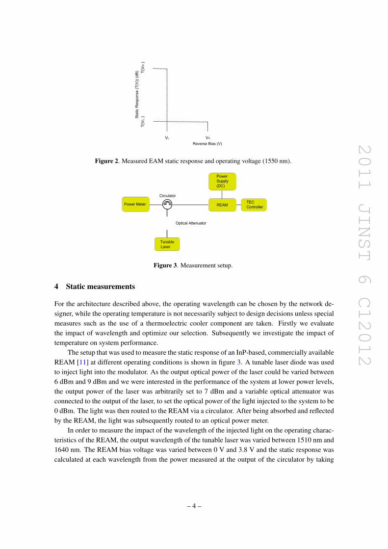
2011 JINST 6 C12012
1510 nm
(a)
Wavelength (nm)
Ove
rall
Pen
alty
(dB
)
Required V
oltage Sw
ing (V
)
(b)
Figure 4 (a) Static response as a function of wavelength and (b) Overall induced penalty due to insertionloss and imperfect extinction ratio vs wavelength (left axis) and required voltage swing vs wavelength(right axis)
into account the connector- and circulator-induced losses at the particular wavelength The resultsof the measurements are shown in figure 4(a) and clearly show that care is needed when choosing abias voltage-wavelength combination to achieve optimum performance in terms of minimizing theinsertion loss of a device and maximizing its extinction ratio To determine the optimum operatingwavelength range we calculated the required voltage swing to achieve the maximum extinction ra-tio (shown in 4(b) right axis) as well as the overall power penalty associated to the extinction ratioand the insertion loss (4(b) left axis) both as a function of wavelength Both the required volt-age swing and the overall penalty should be minimized we have therefore selected the operatingwavelength range to be in the 1550 nm region
The selection of the modulation voltage levels is more challenging in a temperature-varyingenvironment as the static response is temperature-dependent Typically the effects of temperaturevariation are compensated using a thermo-electric cooler (TEC) but for our application this is notacceptable as it would increase the mass and the power consumption of the front-end component
The same measurement methodology that was used to investigate the impact of wavelengthon static response was also utilized to investigate the impact of temperature variation The staticresponse at 1550 nm was measured at three different temperatures (10 C 30 C and 50 C) and theresults are shown in figure 5(a) The temperature range of 40 C has been selected to approximatethe maximum temperature difference inside the detector [6] Figure 5(a) reveals a number of im-portant trends with increasing temperature namely increase of the insertion loss decrease of thereverse bias voltage level at which the static response minimum occurs and a slight increase of themaximum extinction ratio
To assess the impact of temperature it has been assumed that the modulation voltage levels aredetermined by the static response at the highest operating temperature The reason is that the staticresponse minimum occurs at low voltage levels when the operating temperature is high Operationat higher voltages would require the use of both the decreasing and the increasing parts of the staticresponse leading to significant non-linear effects The modulation voltage levels were thus set toVL =minus08 V VHFixed =16 V to maximize the extinction ratio at the highest temperature as shownin figure 5(a) The obvious problem encountered in this case is the sub-optimum choice of voltagelevels at lower temperatures mdash the optimum at 10 C VHOpt =3 V is also shown in figure 5(a)
ndash 5 ndash
2011 JINST 6 C12012
(a) (b)
Figure 5 (a) Temperature Dependence of Static Response and (b) Extinction Ratio Power Penalty VsTemperature for λ=1550 nm
mdash leading to a decrease of the extinction ratio Figure 5(b) shows the calculated extinction ratiopower penalty for different temperatures both when the modulation voltage levels are fixed andwhen optimum voltage levels are used Referring back to the architecture shown in figure 1(a)the additional power penalty results in a decrease in the number of users that can share a singledownstream transmitterCW source combination by a factor of asymp 18 This indicates that somevoltage adaptation mechanism is required to avoid significant performance degradation
5 Dynamic measurements
Although static measurements can provide valuable information regarding the performance bound-aries of the system and allow us to select optimum values of operating parameters with reasonablygood accuracy dynamic measurements are required to validate the feasibility of the system Wefocus on upstream performance as simple link budget calculations using commercial componentvalues show that the maximum number of users that can be served using the architecture of fig-ure 1(a) is determined by the upstream performance constraints Figure 6 shows the setup usedfor the measurements The setup is similar to the one used for the static measurements but with apseudo-random binary sequence (PRBS) source and a wideband amplifier being used to generate a27minus1 10 Gbs PRBS data stream and modulate the voltage applied to the REAM Additionally a10 Gbs PIN photodiode receiver with a pre-amplifier was used instead of a power meter to receivethe modulated light The output of the receiver was connected to a digital communications analyzer(DCA) to view and further analyze the received waveform
The average optical power at the input of the receiver was modified by changing the opticalattenuation at the output of the tunable laser The quality of the signal was measured using thevalue of Q a commonly used indicator for the quality of a modulated signal Q is defined as theratio of the optical power difference between the mark (I1) and space (I0) levels to the summationof the standard deviation (rms values) of noise at the mark (σ1)and space (σ0) levels [10]
Q =I1minus I0
σ1 +σ0(51)
ndash 6 ndash
2011 JINST 6 C12012
Power Supply (DC)
REAMPIN ReceiverTEC Controller
Circulator
WidebandAmplifier
Optical Attenuator
LaserTunable PRBS
Source
DigitalCommunicationsAnalyzer
Figure 6 Dynamic measurement setup
Figure 7 Q-Value and corresponding BER Vs average received power mdash eye diagrams for Q=7 and Q=9(inset)
For noise-limited systems such as ours Q determines the bit error rate (BER) equation 52 [10]
BER =12
erfc(
Qradic2
)asymp
exp(minus Q2
2
)Qradic
2π(52)
where er f c is the complementary error functionThe plot in figure 7 shows the value of Q mdash left axis mdash and the corresponding estimated
BER mdash right axis mdash as a function of the average received optical power The recorded eye dia-grams for Q = 7 (BER = 10minus12) and Q = 9 (BER = 10minus19 that is error-free) are also shown inthe inset of the figure As the diagram shows the required average power to achieve a BER of10minus12 is -164 dBm Referring back to the architecture of figure 1(a) the results suggest that a 10dBm DFB laser can serve 16 users Furthermore measurements of the receiverrsquos thermal noise andcomparison against the specifications of other commercial receivers indicate that a splitting ratioof 132 could be achieved with the use of a higher sensitivity receiver Even without this improve-ment the architecture appears to be cost-efficient in comparison to a point-to-point configurationusing REAMs where one cheap low power laser is used as a CW optical source per REAM Addi-tional cost reduction compared to a point-to-point architecture is achieved due to the downstreamtransmitter sharing
ndash 7 ndash
2011 JINST 6 C12012
6 Summary
We propose a new network architecture for the bidirectional transfer of information in high energyphysics experiments The architecture is based on the use of commercially available REAMs il-luminated remotely by a DFB laser The wavelength-dependent operation of the REAM has beenstudied and we have found that the optimum operating wavelength is in the 1550 nm region Theimpact of temperature variation on REAM operation has also been investigated and we find that thepenalty associated with a 40 C temperature change can be kept below 03 dB with optimum drivevoltage settings The feasibility of the suggested network architecture is demonstrated throughmeasurements of the quality of the received modulated signal at 10 Gbs as a function of its power
Acknowledgments
This work was supported in part by ACEOLE a Marie Curie mobility action at CERN funded bythe European Commission under the 7th Framework Programme The dynamic response measure-ments were carried out at UCL with the help of Dr Manoj Thakur for which we are grateful
References
[1] G Kane and A Pierce Perspectives on LHC physics World Scientific Singapore (2008)
[2] I Papakonstantinou et al A fully bidirectional optical network with latency monitoring capability forthe distribution of timing-trigger and control signals in high-energy physics experiments IEEE TransNucl Sci 58 (2011) 1628
[3] C Da Via et al Lightwave analogue links for lhc detector front-ends Nucl Instrum Meth A 344(1994) 199
[4] A Baird et al Analog lightwave links for detector front-ends at the LHC IEEE Trans Nucl Sci 42(1995) 873
[5] G Aad et al The ATLAS experiment at the CERN LHC 2008 JINST 3 S08003
[6] R Adolphi et al The CMS experiment at the CERN LHC 2008 JINST 3 S08004
[7] S Papadopoulos et al A network architecture for bidirectional data transfer in high-energy physicsexperiments using electroabsorption modulators in proceedings of 16th European Conference onNetworks and Optical Communications July 20ndash22 Northumbria University UK (2011)
[8] G Li and P Yu Optical intensity modulators for digital and analog applications J Lightw Technol21 (2003) 2010
[9] G Ghione Semiconductor devices for high-speed optoelectronics Cambridge University PressCambridge UK (2009)
[10] GP Agrawal Fiber-optic communication systems 3rd edition Wiley New York USA (2002)
[11] Reflective Electroabsorption Modulator type EAM-R-10-C-7S-FCA manufactured by CIP PhotonicsLtd UK see httpwwwciphotonicscom
ndash 8 ndash
- Introduction
- Network architecture
- Electroabsorption modulator
- Static measurements
- Dynamic measurements
- Summary
-
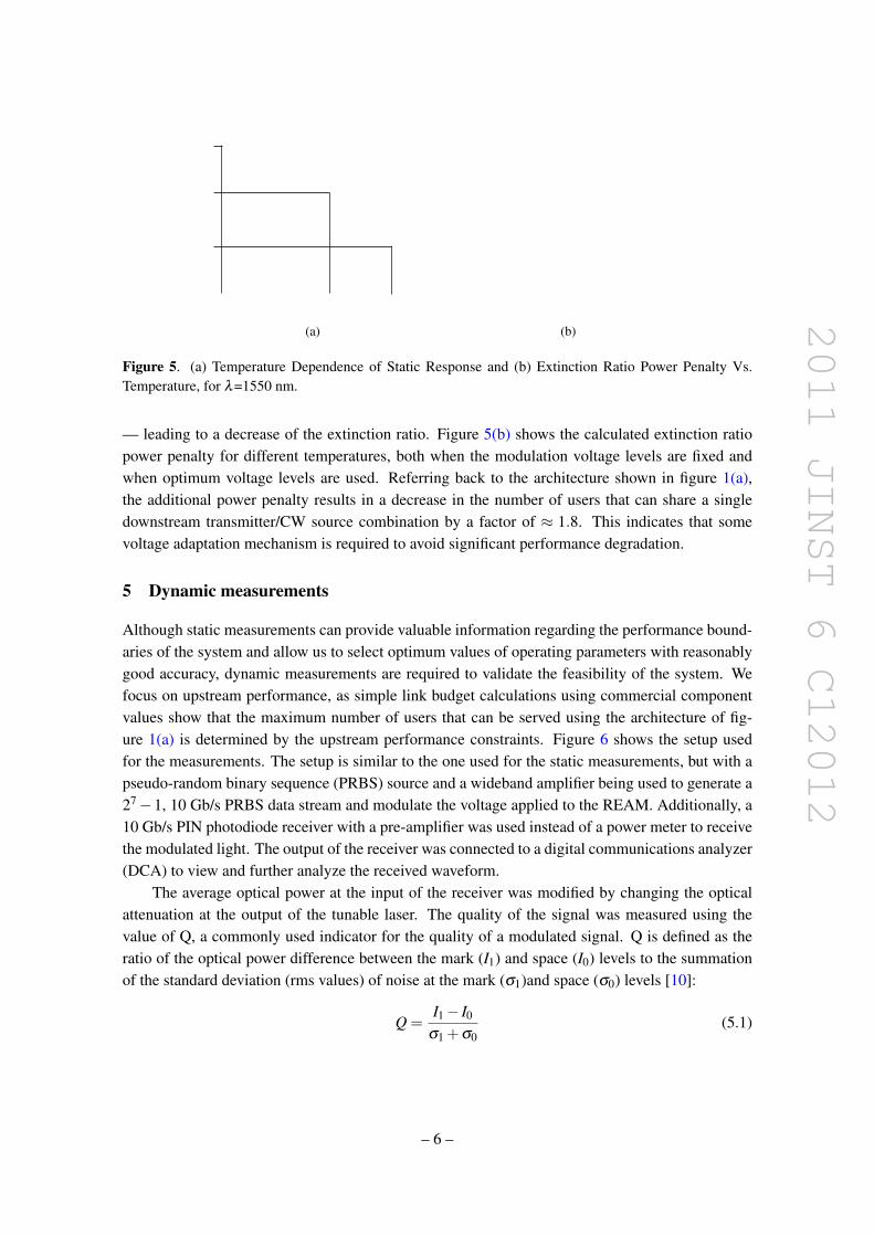
2011 JINST 6 C12012
(a) (b)
Figure 5 (a) Temperature Dependence of Static Response and (b) Extinction Ratio Power Penalty VsTemperature for λ=1550 nm
mdash leading to a decrease of the extinction ratio Figure 5(b) shows the calculated extinction ratiopower penalty for different temperatures both when the modulation voltage levels are fixed andwhen optimum voltage levels are used Referring back to the architecture shown in figure 1(a)the additional power penalty results in a decrease in the number of users that can share a singledownstream transmitterCW source combination by a factor of asymp 18 This indicates that somevoltage adaptation mechanism is required to avoid significant performance degradation
5 Dynamic measurements
Although static measurements can provide valuable information regarding the performance bound-aries of the system and allow us to select optimum values of operating parameters with reasonablygood accuracy dynamic measurements are required to validate the feasibility of the system Wefocus on upstream performance as simple link budget calculations using commercial componentvalues show that the maximum number of users that can be served using the architecture of fig-ure 1(a) is determined by the upstream performance constraints Figure 6 shows the setup usedfor the measurements The setup is similar to the one used for the static measurements but with apseudo-random binary sequence (PRBS) source and a wideband amplifier being used to generate a27minus1 10 Gbs PRBS data stream and modulate the voltage applied to the REAM Additionally a10 Gbs PIN photodiode receiver with a pre-amplifier was used instead of a power meter to receivethe modulated light The output of the receiver was connected to a digital communications analyzer(DCA) to view and further analyze the received waveform
The average optical power at the input of the receiver was modified by changing the opticalattenuation at the output of the tunable laser The quality of the signal was measured using thevalue of Q a commonly used indicator for the quality of a modulated signal Q is defined as theratio of the optical power difference between the mark (I1) and space (I0) levels to the summationof the standard deviation (rms values) of noise at the mark (σ1)and space (σ0) levels [10]
Q =I1minus I0
σ1 +σ0(51)
ndash 6 ndash
2011 JINST 6 C12012
Power Supply (DC)
REAMPIN ReceiverTEC Controller
Circulator
WidebandAmplifier
Optical Attenuator
LaserTunable PRBS
Source
DigitalCommunicationsAnalyzer
Figure 6 Dynamic measurement setup
Figure 7 Q-Value and corresponding BER Vs average received power mdash eye diagrams for Q=7 and Q=9(inset)
For noise-limited systems such as ours Q determines the bit error rate (BER) equation 52 [10]
BER =12
erfc(
Qradic2
)asymp
exp(minus Q2
2
)Qradic
2π(52)
where er f c is the complementary error functionThe plot in figure 7 shows the value of Q mdash left axis mdash and the corresponding estimated
BER mdash right axis mdash as a function of the average received optical power The recorded eye dia-grams for Q = 7 (BER = 10minus12) and Q = 9 (BER = 10minus19 that is error-free) are also shown inthe inset of the figure As the diagram shows the required average power to achieve a BER of10minus12 is -164 dBm Referring back to the architecture of figure 1(a) the results suggest that a 10dBm DFB laser can serve 16 users Furthermore measurements of the receiverrsquos thermal noise andcomparison against the specifications of other commercial receivers indicate that a splitting ratioof 132 could be achieved with the use of a higher sensitivity receiver Even without this improve-ment the architecture appears to be cost-efficient in comparison to a point-to-point configurationusing REAMs where one cheap low power laser is used as a CW optical source per REAM Addi-tional cost reduction compared to a point-to-point architecture is achieved due to the downstreamtransmitter sharing
ndash 7 ndash
2011 JINST 6 C12012
6 Summary
We propose a new network architecture for the bidirectional transfer of information in high energyphysics experiments The architecture is based on the use of commercially available REAMs il-luminated remotely by a DFB laser The wavelength-dependent operation of the REAM has beenstudied and we have found that the optimum operating wavelength is in the 1550 nm region Theimpact of temperature variation on REAM operation has also been investigated and we find that thepenalty associated with a 40 C temperature change can be kept below 03 dB with optimum drivevoltage settings The feasibility of the suggested network architecture is demonstrated throughmeasurements of the quality of the received modulated signal at 10 Gbs as a function of its power
Acknowledgments
This work was supported in part by ACEOLE a Marie Curie mobility action at CERN funded bythe European Commission under the 7th Framework Programme The dynamic response measure-ments were carried out at UCL with the help of Dr Manoj Thakur for which we are grateful
References
[1] G Kane and A Pierce Perspectives on LHC physics World Scientific Singapore (2008)
[2] I Papakonstantinou et al A fully bidirectional optical network with latency monitoring capability forthe distribution of timing-trigger and control signals in high-energy physics experiments IEEE TransNucl Sci 58 (2011) 1628
[3] C Da Via et al Lightwave analogue links for lhc detector front-ends Nucl Instrum Meth A 344(1994) 199
[4] A Baird et al Analog lightwave links for detector front-ends at the LHC IEEE Trans Nucl Sci 42(1995) 873
[5] G Aad et al The ATLAS experiment at the CERN LHC 2008 JINST 3 S08003
[6] R Adolphi et al The CMS experiment at the CERN LHC 2008 JINST 3 S08004
[7] S Papadopoulos et al A network architecture for bidirectional data transfer in high-energy physicsexperiments using electroabsorption modulators in proceedings of 16th European Conference onNetworks and Optical Communications July 20ndash22 Northumbria University UK (2011)
[8] G Li and P Yu Optical intensity modulators for digital and analog applications J Lightw Technol21 (2003) 2010
[9] G Ghione Semiconductor devices for high-speed optoelectronics Cambridge University PressCambridge UK (2009)
[10] GP Agrawal Fiber-optic communication systems 3rd edition Wiley New York USA (2002)
[11] Reflective Electroabsorption Modulator type EAM-R-10-C-7S-FCA manufactured by CIP PhotonicsLtd UK see httpwwwciphotonicscom
ndash 8 ndash
- Introduction
- Network architecture
- Electroabsorption modulator
- Static measurements
- Dynamic measurements
- Summary
-
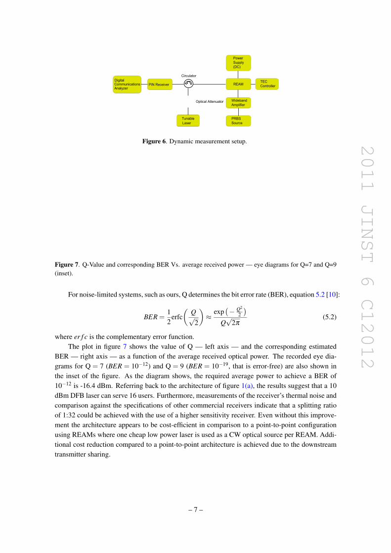
2011 JINST 6 C12012
6 Summary
We propose a new network architecture for the bidirectional transfer of information in high energyphysics experiments The architecture is based on the use of commercially available REAMs il-luminated remotely by a DFB laser The wavelength-dependent operation of the REAM has beenstudied and we have found that the optimum operating wavelength is in the 1550 nm region Theimpact of temperature variation on REAM operation has also been investigated and we find that thepenalty associated with a 40 C temperature change can be kept below 03 dB with optimum drivevoltage settings The feasibility of the suggested network architecture is demonstrated throughmeasurements of the quality of the received modulated signal at 10 Gbs as a function of its power
Acknowledgments
This work was supported in part by ACEOLE a Marie Curie mobility action at CERN funded bythe European Commission under the 7th Framework Programme The dynamic response measure-ments were carried out at UCL with the help of Dr Manoj Thakur for which we are grateful
References
[1] G Kane and A Pierce Perspectives on LHC physics World Scientific Singapore (2008)
[2] I Papakonstantinou et al A fully bidirectional optical network with latency monitoring capability forthe distribution of timing-trigger and control signals in high-energy physics experiments IEEE TransNucl Sci 58 (2011) 1628
[3] C Da Via et al Lightwave analogue links for lhc detector front-ends Nucl Instrum Meth A 344(1994) 199
[4] A Baird et al Analog lightwave links for detector front-ends at the LHC IEEE Trans Nucl Sci 42(1995) 873
[5] G Aad et al The ATLAS experiment at the CERN LHC 2008 JINST 3 S08003
[6] R Adolphi et al The CMS experiment at the CERN LHC 2008 JINST 3 S08004
[7] S Papadopoulos et al A network architecture for bidirectional data transfer in high-energy physicsexperiments using electroabsorption modulators in proceedings of 16th European Conference onNetworks and Optical Communications July 20ndash22 Northumbria University UK (2011)
[8] G Li and P Yu Optical intensity modulators for digital and analog applications J Lightw Technol21 (2003) 2010
[9] G Ghione Semiconductor devices for high-speed optoelectronics Cambridge University PressCambridge UK (2009)
[10] GP Agrawal Fiber-optic communication systems 3rd edition Wiley New York USA (2002)
[11] Reflective Electroabsorption Modulator type EAM-R-10-C-7S-FCA manufactured by CIP PhotonicsLtd UK see httpwwwciphotonicscom
ndash 8 ndash
- Introduction
- Network architecture
- Electroabsorption modulator
- Static measurements
- Dynamic measurements
- Summary
-