an integrated circuit for feedback control & compensation
TRANSCRIPT

An Integrated Circuit for Feedback Control &
Compensation of an Organic LED Displayby
Kartik S. LambaSubmitted to the Department of Electrical Engineering and Computer
Sciencein partial fulfillment of the requirements for the degree of
Master of Engineering in Electrical Engineering and Computer Science
at the
MASSACHUSETT EJNSTITUTX OF TECHNOLOGY
Fbruary 2096
@ Kartik S. Lamba, MMVI. All rights reserved.
The author hereby grants to MIT permission to reproduce anddistribute publicly paper and electronic copies of this thesis document
in whole or in part. IMASSACHUSETTS
Author . , . . . . . . . . . . . . . . . . . . . . . . . . . . . . . . . . . . . . .Oe~rtent of Electrica ngineering and Computer Science
Certified by l . . . ....
.4
Certified by
Accepted by
.......
February 21, 2006
.. ............ .....
Charles G. SodiniProfessor
Thesis Supervisor
.............. .....Vladimir Bulovic
Associate Professoresis Supervisor
.. .. . . . ...... .. .....
Arthur C. SmithChairman, Department Committee on Graduate Students
ARCHNES
OF TECHNOLOGY
AU 1S4 2006
LtBRARIES
wlnn" I
.

2

An Integrated Circuit for Feedback Control & Compensation
of an Organic LED Display
by
Kartik S. Lamba
Submitted to the Department of Electrical Engineering and Computer Scienceon February 21, 2006, in partial fulfillment of the
requirements for the degree ofMaster of Engineering in Electrical Engineering and Computer Science
Abstract
Organic LEDs (OLEDs) have the potential to be used to build large-format, thin,flexible displays. Currently, the primary drawback to their usage lies in the difficultyof producing OLEDs which emit light at a constant and predictable brightness overtheir lifetime. A solution has been proposed which uses organic photo-detectors andoptical feedback to control the desired luminosity on a per-pixel basis. This thesisdemonstrates the design and fabrication of an integrated silicon control chip andan organic pixel/imaging array, which together form a stable, usable display. Thesimulation, verification, and testing of this OLED display demonstrates the utilityof our solution. In particular, this thesis focuses on the Loop Compensator silicondesign and feedback aspects of this circuit. The results demonstrate that the LoopCompensator has the desired DC and frequency characteristics with a measured gainof 100.2 and a variable dominant pole located at digitally-selectable frequencies (usinga programmable capacitor array) of 10.8 Hz, 13.5 Hz, 22.8 Hz, and 64.8 Hz, given aclock frequency of 20 kHz.
Thesis Supervisor: Charles G. SodiniTitle: Professor
Thesis Supervisor: Vladimir BulovicTitle: Associate Professor
3

4

Acknowledgments
I would like to thank several people without whom this thesis would not be possible:
My academic and research advisor, Prof. Charles G. Sodini, who supported and
guided me through this entire process.
My associate research advisor, Prof. Vladimir Bulovic, for offering me a second
perspective.
My colleague and friend Albert Lin, who designed the silicon chip with me, and
made it easier to work those long nights before a tape-out deadline.
Peter Holloway, Sangamesh Buddhiraju, and everyone else at National Semicon-
ductor for offering countless hours of technical and design help, and of course, fabri-
cating two of our chips, with nothing but a sincere "Thank You" in return.
Kevin Ryu, Jennifer Yu, Joannis Kymissis, and everyone else who attended our
weekly meetings and provided valuable insight into this project.
In addition, I would like to thank my parents Hari and Suman Lamba for support-
ing me both financially and emotionally throughout my time at MIT, and for always
pushing me to do my best.
Finally, I would like to thank all of my colleagues and friends in the Sodini and
Lee research groups who were always there at all times of the night and day to answer
my questions, and who really made these past years enjoyable.
This work was funded in part by C2S2, the MARCO Focus Center for Circuit &
Systems Solutions, under the MARCO contract 2003-CT-888.
5

THIS PAGE INTENTIONALLY LEFT BLANK
6
Contents
1 Introduction
1.1 Thesis Objectives & Motivation . . . . . . . . . . . . . . . . . . . . .
1.2 Thesis Organization. . . . . . . . . . . . . . . . . . . . . . . . . . . .
2 Background
2.1 Liquid Crystal Display Overview . . . . . . . . . . . . . . . . . . . .
2.2 OLED Display Overview . . . . . . . . . . . . . . . . . . . . . . . . .
2.2.1 OLED Display Advantages . . . . . . . . . . . . . . . . . . . .
2.2.2 OLED Display Disadvantages . . . . . . . . . . . . . . . . . .
2.2.3 Modern OLED Displays . . . . . . . . . . . . . . . . . . . . .
3 Organic Integrated Circuit Design
3.1 Organic Architecture and Specifications . . . . . . . . . . . . . . . . .
3.1.1 A Pixel/Sensor: A Single OLED/OPD . . . . . . . . . . . . .
3.1.2 A Display/Imager: An Array of OLED/OPDs . . . . . . . . .
3.2 Discrete Component Model . . . . . . . . . . . . . . . . . . . . . . .
4 OLED Optical Feedback Solution
4.1 General Description .........
4.2 Prior Optical Feedback Solutions
4.3 Thesis System Implementation .
4.4 Feedback/MATLAB Analysis
7
13
14
14
15
15
16
16
16
17
19
19
20
21
23
25
25
25
26
28
. . . . . . . . . . .
. . . . . . . . . . .
. . . . . . . . . . .
. . . . . . . . . . .

5 Silicon Integrated Circuit Design
5.1 Silicon Architecture and Specifications . . . . . . . . . . . . .
5.2 Summing Junction Block . . . . . . . . . . . . . . . . . . . . .
5.3 G ain B lock . . . . . . . . . . . . . . . . . . . . . . . . . . . .
5.4 Dominant-Pole Compensation Block (Variable Pole Location)
5.4.1 Programmable Capacitor Array (PCA) . . . . . . . . .
5.5 Operational Amplifier Design . . . . . . . . . . . . . . . . . .
5.6 Output Multiplexer . . . . . . . . . . . . . . . . . . . . . . . .
6 Integrated Silicon Chip Results
6.1 Silicon Chip Overview . . . . . . . . . . . . .
6.2 Test Setup . . . . . . . . . . . . . . . . . . . .
6.3 Measurements & Results . . . . . . . . . . . .
6.3.1 DC Measurements . . . . . . . . . . .
6.3.2 AC Measurements . . . . . . . . . . .
6.3.3 Other Measurements . . . . . . . . . .
7 Conclusions
8
31
32
33
34
36
37
38
38
41
. . . . . . . . . . . 41
. . . . . . . . . . . 43
. . . . . . . . . . . 44
. . . . . . . . . . . 45
. . . . . . . . . . . 50
. . . . . . . . . . . 52
53

List of Figures
2-1 Cadence OLED-on-Silicon Display Driver . . . . . . . . . . . . . . . .
3-1 OPD/OFET Die Photo . . . . . . . . . . . . . . . . . . . . . . . . . .
3-2 Organic Pixel/Sensor Circuit Model . . . . . . . . . . . . . . . . . . .
3-3 Column-Parallel Architecture . . . . . . . . . . . . . . . . . . . . . .
3-4 Discrete Circuit Model . . . . . . . . . . . . . . . . . . . . . . . . . .
3-5 Discrete Pixel Model IV Characteristics. The two separate lines in this
graph represent the limits of the adjustable attenuator. . . . . . . . .
4-1 General Optical Feedback Solution . . . . . . . . . . . . . . . . . . .
4-2 System Block Diagram . . . . . . . . . . . . . . . . . . . . . . . . . .
4-3 Integrated Organic & Silicon System Block Diagram . . . . . . . . . .
4-4 Feedback System Diagram . . . . . . . . . . . . . . . . . . . . . . . .
4-5 Feedback System Bode Plot . . . . . . . . . . . . . . . . . . . . . . .
5-1
5-2
5-3
5-4
5-5
5-6
5-7
5-8
System Block Diagram . . . . . . . . . . . . . . . . . . . .
Loop Compensator Block Diagram . . . . . . . . . . . . .
Summing Junction Circuit Diagram . . . . . . . . . . . . .
Gain Block Circuit Diagram . . . . . . . . . . . . . . . . .
Dominant-Pole Block Circuit Diagram . . . . . . . . . . .
Programmable-Capacitor-Array (PCA) for Adjustable Pole
Operational Amplifier (1pF load) Circuit Diagram . . . . .
Output M ultiplexer . . . . . . . . . . . . . . . . . . . . . .
6-1 Silicon Chip (MITOLEDB) Die Photo . . . . . . . . . . .
9
17
20
21
22
23
24
25
27
27
28
29
. . . . 31
. . . . 32
. . . . 34
. . . . 35
. . . . 36
. . . . 38
. . . . 39
. . . . 40
42

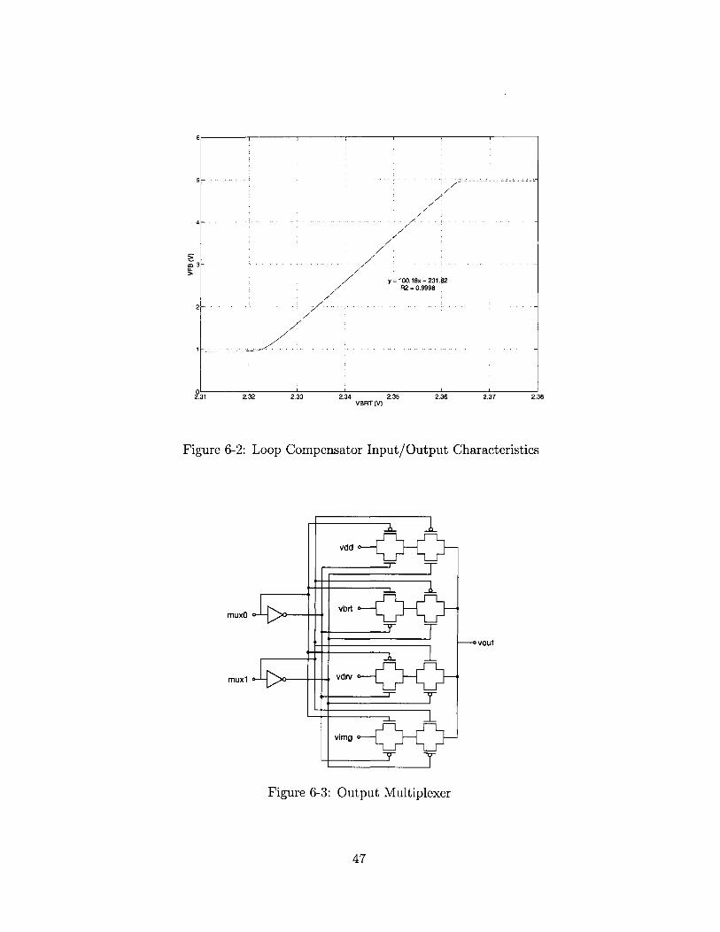
6-2 Loop Compensator Input/Output Characteristics . . . . . . . . . . . 47
6-3 Output M ultiplexer . . . . . . . . . . . . . . . . . . . . . . . . . . . . 47
6-4 Silicon Chip Ground Model [10] . . . . . . . . . . . . . . . . . . . . . 48
6-5 Dominant Pole Block with Non-Functional clk1 Signal . . . . . . . . 49
6-6 DC Sweep Simulation of Dominant Pole Block with clk1 = OV . . . . 50
6-7 Loop Compensator Frequency Characteristics f,, = 20kHz . . . . . . 51
10
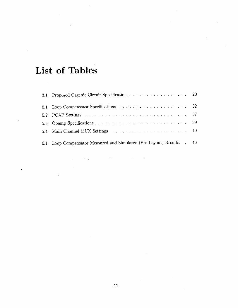
List of Tables
3.1 Proposed Organic Circuit Specifications . . . . . . . . . . . . . . . . . 20
5.1 Loop Compensator Specifications . . . . . . . . . . . . . . . . . . . . 32
5.2 PCAP Settings . . . . . . . . . . . . . . . . . . . . . . . . . . . . . . 37
5.3 Opamp Specifications . . . . . . . . . . . . . .'. . . . . . . . . . . . . 39
5.4 Main Channel MUX Settings . . . . . . . . . . . . . . . . . . . . . . 40
6.1 Loop Compensator Measured and Simulated (Pre-Layout) Results. . 46
11

THIS PAGE INTENTIONALLY LEFT BLANK
12

Chapter 1
Introduction
An essential part of modern electronics is the display. It is one of the most intuitive
and user-friendly methods of communicating information. Large-format displays are
particularly useful when there is a copious amount of data, or when the intended
audience is distributed over a sizable zone. The telecommunications industry, for
example, uses large-format displays to visualize massive amounts of data at full scale
in order to monitor their networks and services. Modern sports venues are increasingly
using larger displays to convey interactive game information and advertisements from
their sponsors. Even highway billboards have evolved from static signs to dynamic,
animated displays. High-resolution, large-format displays are crucial in presenting
this information properly [1].
Unfortunately, current electronic display technologies cannot easily be scaled to
these large dimensions. Current solutions typically involve tiling many displays to-
gether to form a wall of images. While graphics hardware exists to support these kinds
of visualizations, the displays themselves are not flexible, power-efficient, or portable.
The most prevalent display technology is the Liquid Crystal Display (LCD). As a ma-
ture technology, however, LCDs have many limitations which can greatly influence the
overall system design. These drawbacks include power inefficiency, size limitations,
and the physical inflexibility of the display.
An Organic Light Emitting Diode (OLED) display is a technology in its rela-
tive infancy, but offers a promising solution for large-format, low-power, inexpensive
13
displays. However, the voltage-to-light characteristics of OLEDs are still difficult to
match from device-to-device, and can degrade significantly over time. This disadvan-
tage severely limits the display functionality and lifetime (~1000 hours) [2].
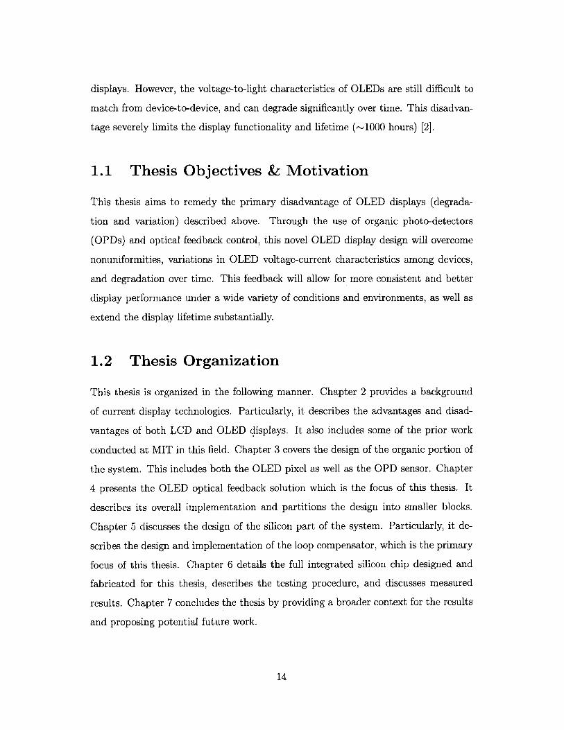
1.1 Thesis Objectives & Motivation
This thesis aims to remedy the primary disadvantage of OLED displays (degrada-
tion and variation) described above. Through the use of organic photo-detectors
(OPDs) and optical feedback control, this novel OLED display design will overcome
nonuniformities, variations in OLED voltage-current characteristics among devices,
and degradation over time. This feedback will allow for more consistent and better
display performance under a wide variety of conditions and environments, as well as
extend the display lifetime substantially.
1.2 Thesis Organization
This thesis is organized in the following manner. Chapter 2 provides a background
of current display technologies. Particularly, it describes the advantages and disad-
vantages of both LCD and OLED displays. It also includes some of the prior work
conducted at MIT in this field. Chapter 3 covers the design of the organic portion of
the system. This includes both the OLED pixel as well as the OPD sensor. Chapter
4 presents the OLED optical feedback solution which is the focus of this thesis. It
describes its overall implementation and partitions the design into smaller blocks.
Chapter 5 discusses the design of the silicon part of the system. Particularly, it de-
scribes the design and implementation of the loop compensator, which is the primary
focus of this thesis. Chapter 6 details the full integrated silicon chip designed and
fabricated for this thesis, describes the testing procedure, and discusses measured
results. Chapter 7 concludes the thesis by providing a broader context for the results
and proposing potential future work.
14
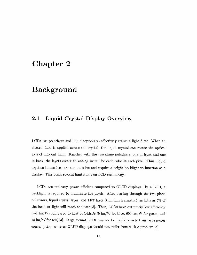
Chapter 2
Background
2.1 Liquid Crystal Display Overview
LCDs use polarizers and liquid crystals to effectively create a light filter. When an
electric field is applied across the crystal, the liquid crystal can rotate the optical
axis of incident light. Together with the two plane polarizers, one in front and one
in back, the layers create an analog switch for each color at each pixel. Thus, liquid
crystals themselves are non-emissive and require a bright backlight to function as a
display. This poses several limitations on LCD technology.
LCDs are not very power efficient compared to OLED displays. In a LCD, a
backlight is required to illuminate the pixels. After passing through the two plane
polarizers, liquid crystal layer, and TFT layer (thin film transistor), as little as 5% of
the incident light will reach the user [3]. Thus, LCDs have extremely low efficiency
(-1 lm/W) compared to that of OLEDs (5 lm/W for blue, 600 lm/W for green, and
15 lm/W for red) [4]. Large-format LCDs may not be feasible due to their large power
consumption, whereas OLED displays should not suffer from such a problem [5].
15
2.2 OLED Display Overview
2.2.1 OLED Display Advantages
OLED displays present a solution to all of the issues raised above and offer an exciting
alternative to LCDs. As a direct emission technology, OLED displays are not only
much more power efficient than LCDs, but they also don't suffer from viewing-angle
limitations. Additionally, the scalability of OLEDs make it much easier to create
large displays several meters in size.
Other advantages of OLED displays include flexibility and cost efficiency. OLEDs
are inherently thinner devices (-1 micron in thickness) than LCDs and can be fabri-
cated on thin substrates such as plastic, permitting curved and flexible displays. In
addition, OLEDs and organic transistors can be fabricated using processes much sim-
pler and cheaper than silicon processes, and typically at room temperature. Thus, an
all-organic OLED display can be easily scaled for large-area displays, such as posters
or billboards [6].
Research on organic optoelectronics over the past two decades has advanced
OLEDs significantly to render them suitable for a display technology. Power efficien-
cies have increased from 0.1-1 lm/W to 10-100 lm/W. And new topologies, techniques,
and organics have allowed OLEDs to become much more stable. Already, there are a
few corporations that have begun to commercialize OLED display technology [7].
2.2.2 OLED Display Disadvantages
Unfortunately, the development of OLED displays is behind that of LCDs. Although
the field of Organic Optoelectronics has been an active research field for nearly two
decades, the current state of organic transistors (OFETs) is similar to that of transis-
tors in the 1960s. In order to create a fully organic display, OFETs are necessary for
such purposes as driving and selecting particular OLEDs. Fabricating OLEDs with
low operating voltages and a lifetime suitable for commercial use has been difficult to
achieve. It was not until 1987 that the first vacuum-deposited OLEDs with practical
16

Murn -- oi Contrast
VIN + DACREF Brightness
500uA 500uA
IOUT Nominal output current:5-500uA
Figure 2-1: Cadence OLED-on-Silicon Display Driver
operating voltages were successfully demonstrated [8]. However, the voltage-to-light
characteristics of OLEDs are still difficult to match from device-to-device, and can
degrade significantly over time. This disadvantage severely limits the display func-
tionality and lifetime (~1000 hours) [2].
After such a short time, the OLEDs degrade and the display produces nonuniform
brightness and contrast. Current solutions address the issue of non-uniformity, but
they simply do not address the problem of OLED degradation as a function of time,
use, and environmental factors. Degradation is one of the main barriers to widespread
OLED display commercialization. Thus, OLED displays have found their way into
simple, small applications, but not yet into large-format displays.
2.2.3 Modern OLED Displays
In 2003, Kodak released the first digital camera with an OLED display, and Sanyo
jointly developed with Kodak a 15" OLED display monitor. In addition, some cell
phones and watches are already beginning to use OLED displays in Japan and Korea.
LG has a cell phone with an OLED display, and Sony has a MP3 player with a similar
feature. To combat OLED non-uniformity, much effort has been taken to develop
uniform OLEDs and a method of driving the OLEDs with predictable or constant
currents.
Cadence Design Systems has come up with one particular solution to this problem.
17

An example circuit demonstrating this solution is shown in Figure 2-1 [9]. The input
of this circuit is a voltage between 0 and 700mV from a standard computer video
card which corresponds to a particular red, green, or blue level. This voltage is first
converted to a current using an amplifier, NMOS device and calibrated resistor R 1.
The range of this current IREF is between 0 and 500pA. IREF is then added to a
precise, externally calibrated current source I, = 500pA. This reduces the settling
time in the next stage which is a multiplying current DAC. This block uses a digital
contrast input to adjust the gain (contrast) of the current input by as much as ±50%.
A digital brightness input then sets a current DAC to offset the current output by as
much as ±500pA. A second 500pA current source is then used to remove the initial
added offset. Finally, the current output IOUT is a precise, digitally scaled and offset
version of the original input video voltage, and is used to drive a particular red, green,
or blue OLED.
18

Chapter 3
Organic Integrated Circuit Design
While this thesis does not explicitly focus on the design of the organic system, it is
important to understand how it was designed and its specifications, particularly those
aspects relevant to the silicon chip. This chapter describes the design of this organic
integrated circuit, which forms the physical display and is controlled and driven by
the silicon circuitry.
3.1 Organic Architecture and Specifications
The proposed organic integrated circuit is a 64 by 64 pixel display. The chip consists
of several layers of organic chemicals and metals which together form devices that
produce and detect light (OLEDs and OPDs, respectively), as well as modulate elec-
trical signals (OFETs). A die photo of an OPD in series with an OFET is shown in
Figure 3-1. For a much more detailed description on how these devices are fabricated
on the chemical level, consult Yu's thesis [6].
The display was designed with a number of considerations in mind. A 64 by 64
pixel array was chosen for two reasons. Firstly, the number of rows in the display
is limited by the required refresh rate. The settling time of each row multiplied by
the number of rows determines how long it takes to refresh the entire display, as
discussed in Section 4.4. Secondly, the number of columns in the display are limited
by the desired complexity of the whole system. Each silicon chip can control sixteen
19
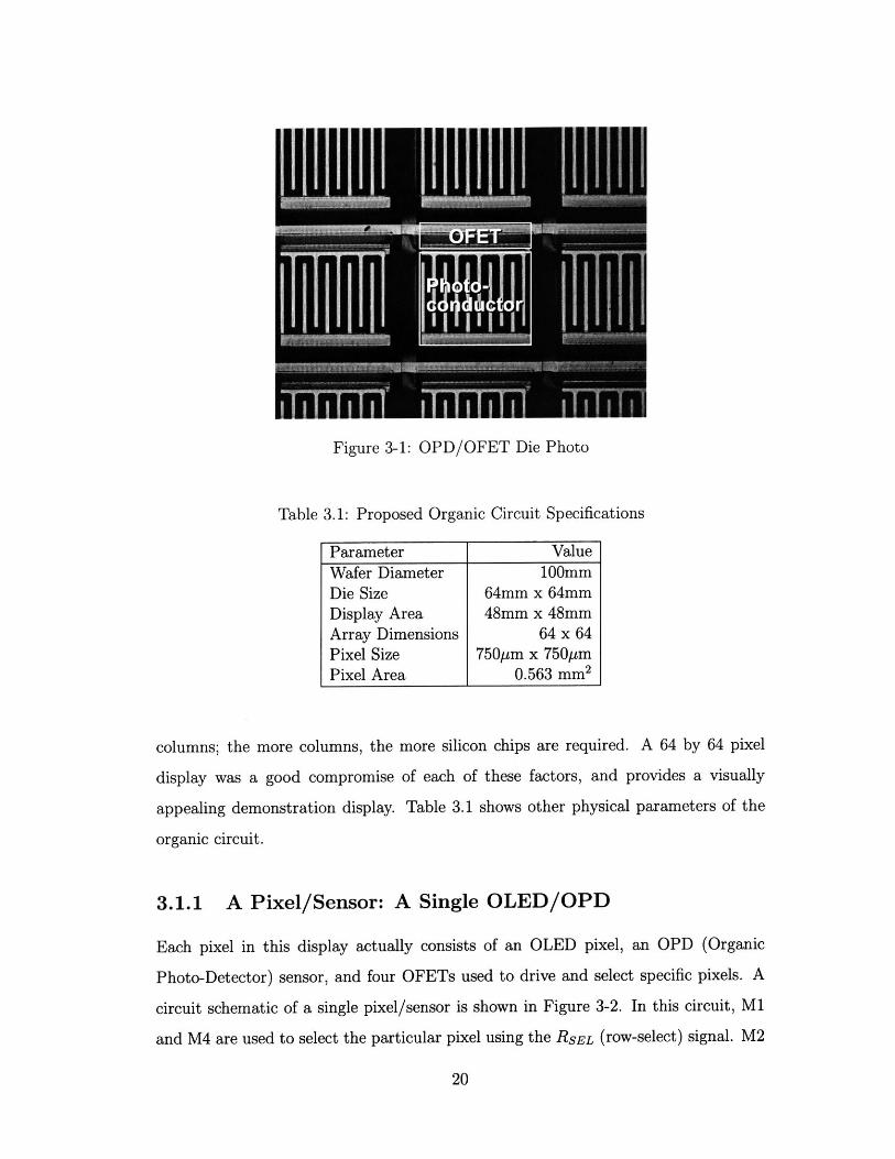
Figure 3-1: OPD/OFET Die Photo
Table 3.1: Proposed Organic Circuit Specifications
columns; the more columns, the more silicon chips are required. A 64 by 64 pixel
display was a good compromise of each of these factors, and provides a visually
appealing demonstration display. Table 3.1 shows other physical parameters of the
organic circuit.
3.1.1 A Pixel/Sensor: A Single OLED/OPD
Each pixel in this display actually consists of an OLED pixel, an OPD (Organic
Photo-Detector) sensor, and four OFETs used to drive and select specific pixels. A
circuit schematic of a single pixel/sensor is shown in Figure 3-2. In this circuit, M1
and M4 are used to select the particular pixel using the RSEL (row-select) signal. M2
20
Parameter ValueWafer Diameter 100mmDie Size 64mm x 64mmDisplay Area 48mm x 48mmArray Dimensions 64 x 64Pixel Size 750pam x 750p.mPixel Area 0.563 mm2

RSEL 0
RSEL +20V
VDRV o M3 M4M1 M2
OLED Y
GND * IOUT
Figure 3-2: Organic Pixel/Sensor Circuit Model
is used to mitigate charge injection on RSEL transitions. M3 is considerably larger
than the other three as it is used to drive the OLED. The OPD measures the incident
light and produces a linearly proportional current IOUT, which in turn is linearly
proportional to the current through the OLED (IOLED).
There are two significant poles that dominate the frequency characteristics of this
circuit. The first is at the gate of M3. It is due to the large gate capacitance of M3
(due to its current-driving requirement) in series with the on-resistance of M1. This
is modeled to be on the order of 10kHz (roughly 10OOpF in parallel with 10kQ). The
second is at the drain of M3. This pole is due to the capacitance of the OLED in
parallel with its output resistance and the output resistance of M3. This is modeled
to be on the order of 100kHz (roughly 100pF in parallel with 10kQ). It is important
to remember that these are estimated numbers and depend highly on both organic
processing technology and the physical display parameters in Table 3.1.
3.1.2 A Display/Imager: An Array of OLED/OPDs
In order to design a functional display without creating separate drivers and sensors
for each individual pixel (212 total for this relatively small display), a column-parallel
architecture is used. A circuit schematic of an example 3 by 3 pixel display using
21

VBRT#
Loop Current-SensingComenator Amplifier
VBRT,
CoLnstor Current-SensingCo44sao Amplifier
VBRT#
LoOp Current-SensingCompensator Amplifier
:11 LvzI___
RSEL#
RSEL#
RSELO
-IJThTh~
Figure 3-3: Column-Parallel Architecture
such an architecture is shown in Figure 3-3. In this architecture, one silicon circuit
is used to control an entire column of organic pixels. Digital input lines are used to
select a particular row. A full frame is produced in the following manner:
1. The first row is selected by setting the first signal (RSEL1). Each of the 16
VBRT# signals are set to an analog value correseponding to a particular pixel
brightness.
2. Each of the 16 silicon circuits sense IOUT of the OPD and servo VDRV accord-
ingly. This feedback loop is given a fixed amount of time to settle.
3. The second row is selected and the first row is deselected. At this point, the
gate capacitances of the drive transistors (M3) must hold the voltages which
correspond to the desired pixel brightnesses during the time when this row is
not in feedback. The assumption made here is that the leakage current from
this capacitor (determined by the subthreshold current through M1 and any
22
IIT1 1a.

+5V
lk(160) lk(160) 1k(320)VDRV 01-/f ) ) BSS92
100nF 4.7nF 2 7 0pF
MPQ390415M
" GND
3 adjustable poles Widlar current High-impedancemirror/attenuator output stage
Figure 3-4: Discrete Circuit Model
parasitic leakage paths due to inadequate isolation) is small enough to not
significantly change the gate voltage of M3 during one refresh cycle.
4. Again, each of the 16 silicon circuits sense IOUT of the OPD and servo VDRV
accordingly, this time for row 2.
5. Steps 3 and 4 are repeated for the remaining rows in the display. Once a full
frame has been updated, the process repeats again starting with row 1.
3.2 Discrete Component Model
Since the integrated organic circuit was not available to test at the time of this thesis,
a substitute circuit was designed and built using only discrete components. This
circuit is shown in Figure 3-4 and was designed with the following characteristics in
mind. In general, these characteristics are intended to be equivalent to the organic
circuit, with the exception that the input range was reduced to 0-5V (from 0-20V) to
make the implementation easier:
. Input: 0-5V
23

1 -- - ------- - - - -- - -
6-
04-
2-.
0-
-200 05 1 1.5 2 !5 3 3.5 4 4.5 5
VDRV (V)
Figure 3-5: Discrete Pixel Model IV Characteristics. The two separate lines in thisgraph represent the limits of the adjustable attenuator.
* 3 externally adjustable poles (-1OkHz, -100kHz, -1MHz)
* Externally adjustable attenuation factor (- -2 - 10-9Q-1)
* Internal mapping: OV-1OnA, 5V-+OnA
* Output: 0-10nA, voltage bias: ~2.5V
This circuit consists of three tunable poles, a PMOS input stage and V-I converter,
an adjustable current mirror/attenuator using matched discrete BJTs, and a high-
impedance current output stage. The tunable poles are used to model the dynamics
of the organic circuit. The PMOS input device (BSS92) models the organic p-type V-
I converter. The MPQ3904 and MPQ3906 matched BJT devices serve to mirror and
attenuate the PMOS drain current down to 10nA levels at the output. A variable
attenuation factor is provided by using a 15MQ potentiometer. This mirror also
provides a high-impedance current output at the IOUT node. This output impedance
is 9 (the early voltage divided by the output collector current) which is roughly
7A = 5GQ. A DC measurement of this circuit is shown in Figure 3-5.
24

Chapter 4
OLED Optical Feedback Solution
4.1 General Description
This thesis utilizes a technique to improve OLED display quality and lifetime. The
most general technique uses optical feedback on the pixel level to stabilize the display.
It pairs each OLED pixel with a light sensor which directly measures the amount of
incident light. This measurement can then be used to adjust the circuit driving the
OLED pixel. Figure 4-1 shows a block diagram of this feedback circuit.
4.2 Prior Optical Feedback Solutions
A number of students at MIT have previously explored using this technique in various
ways. Eko Lisuwandi first implemented the optical feedback solution design in his
'" Compensator OLED Light
LightAmplifier Sensor'*
Figure 4-1: General Optical Feedback Solution
25

Master's thesis [3]. His research explored and confirmed the feasibility of an optical
feedback solution to stabilize the brightness of an OLED display. Lisuwandi built
a discrete version of the feedback circuitry for a 5 by 5 OLED array. An external
camera was used as the light sensor for the optical feedback. His results demonstrated
that the optical feedback design is a promising solution for OLED displays.
Matthew R. Powell continued Lisuwandi's work in designing and revising an in-
tegrated version of the circuit [4]. The design was an all-silicon design except for the
OLEDs, which were deposited on the chip in a separate organic process. Jennifer J.
Yu developed the organic-on-silicon process [6]. The photo-detectors (silicon photo-
diodes) and the feedback circuits were integrated with the addressing and driver cir-
cuits on a single chip. The chip features a 128 by 16 pixel array in a column-parallel
architecture (1 feedback loop per column). This integration of silicon and organic
circuits on the same substrate, while unique, posed numerous testing difficulties and
limits in size.
4.3 Thesis System Implementation
This thesis goes a step further from the previous work. See Figure 4-2 for a system
feedback block diagram. This implementation splits the design into two integrated
chips: one silicon and one organic. The integrated organic chip contains an array
of OLEDs which together form the display. Each OLED is paired with an organic
photo-detector (OPD) which measures the incident light. See Chapter 3 for details
about this design. The integrated silicon chip contains two primary blocks which
together amplify the OPD output, compensate the loop, and drive the OLED. See
Chapter 5 for details about this implementation.
Figure 4-3 depicts a theoretical system using the silicon and organic components
introduced above. Each silicon chip contains 16 channels, each controlling one column
in a display. This is referred to as a column-parallel architecture, which is covered
in Section 3.1.2. As discussed later in this chapter, with this particular architecture,
the poles of the organic circuit (see Chapter 3) along with display refresh rate spec-
26

Silicon Organic/Discrete
VBRT ' Summing Gain Gain Dominant Pole OLED LightJunction -+Stage -- + Stage - 10Hz (Variable) Pixel
+ -lox -1ox -1x -lx
Display
Imager
Sample Diff->Sing Gain Transimpedance Organic& Hold Conversion Stage - Stage Stage Photodetector-lx 5x (Variable) lox 107x (OPD)
Figure 4-2: System Block Diagram
vbrt (16) brt (16)vbrt (16) vbrt (16)
Si Si Si Si
Computer/ Organic d >(16) io(16) vd(16) 'o(16) vd(16) 0(16)
FPGA ,.et Display
64
32
32
16 16 16 16
vd(16) o() vd (16) io (16) vd() io(16) vd(16) l o (16)
ync i S i S
Figure 4-3: Integrated Organic & Silicon System Block Diagram
27

VBR s _V10 KEXT= I- OE IOLED0_O5V - DPS+l 0-VIKET -20V TrOFETS+l LD
------------- 4 (LighA
3O-OSa 1 InA S
H KFB=- 5 04VCOA KCSA=l e7 KCS AOPD
Figure 4-4: Feedback System Diagram
ifications limit the number of rows one chip can control to 32 rows. Thus, in this
system, each silicon chip can control a 32 by 16 portion of a display. In order to drive
a 64 by 64 organic display depicted here, 8 silicon chips are required. A computer or
FPGA-based system controls all of the timing and synchronization signals.
4.4 Feedback/MATLAB Analysis
In order to understand how to design a robust loop compensator, one must fully
understand the frequency characteristics of the rest of the system and how they
pertain to the loop. Figure 4-4 shows a feedback block diagram for the entire system.
As is discussed in Chapter 3, the most uncertain part of the system is the organic
part of this loop. We can simplify this part by modeling it as a two-pole system, with
poles at estimated values of 10kHz and 100kHz. Derivations of these numbers are
described in Chapter 3, though they are crude estimates and should be expected to
vary by up to an order of magnitude. Additionally, the gain of the organic circuit,
modeled here by KOLED and KOPD will also potentially deviate from expected values.
In order to handle these variations, the silicon circuits must be designed to be
as robust as possible. To assist with this, parts of the silicon design use external
digital signals to modify its own gain and frequency characteristics over larger ranges.
The loop compensator employs a dominant-pole system implemented using a switch-
capacitor architecture and is discussed in detail in Chapter 5. This compensator
28
10' -- ------ T =.7 -T r 1 ---F T "r ------
10
f 1kHz
1 0 --- -.-.-- -- .-.- -
10
$ 84P
-13
.. .. . ....8 .
--180' 7-- --- - - - -
270t
-3151 - -- ..
--3 6 0 1 -....... - - .... -.. -.- .- ,..,10 IC 10 10 10- 10 10 10 10
Frequency (Hz)
Figure 4-5: Feedback System Bode Plot
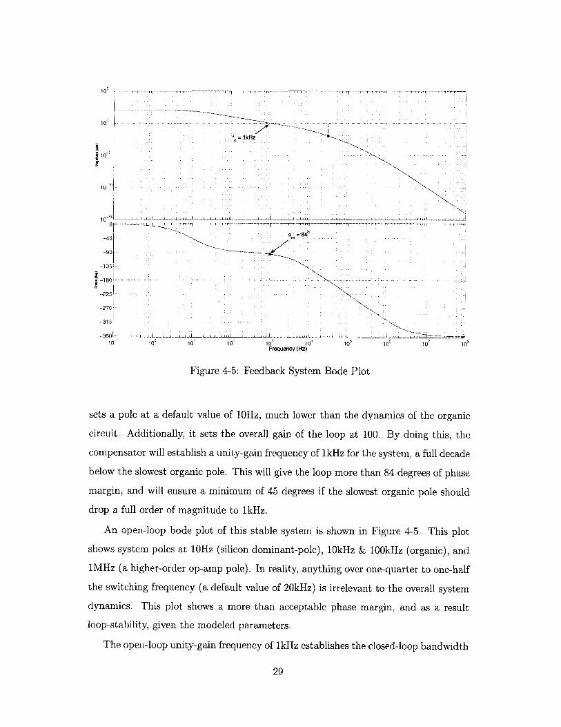
sets a pole at a default value of 10Hz, much lower than the dynamics of the organic
circuit. Additionally, it sets the overall gain of the loop at 100. By doing this, the
compensator will establish a unity-gain frequency of 1kHz for the system, a full decade
below the slowest organic pole. This will give the loop more than 84 degrees of phase
margin, and will ensure a minimum of 45 degrees if the slowest organic pole should
drop a full order of magnitude to 1kHz.
An open-loop bode plot of this stable system is shown in Figure 4-5. This plot
shows system poles at 10Hz (silicon dominant-pole), 10kHz & 100kHz (organic), and
1MHz (a higher-order op-amp pole). In reality, anything over one-quarter to one-half
the switching frequency (a default value of 20kHz) is irrelevant to the overall system
dynamics. This plot shows a more than acceptable phase margin, and as a result
loop-stability, given the modeled parameters.
The open-loop unity-gain frequency of 1kHz establishes the closed-loop bandwidth
29

at this same value. This sets the system time-constant at r=lms. Allowing for a
minimum of 5 time-constants for the loop to settle means the system must be given
5ms for each row to establish a desired pixel light output. Since in this column-parallel
architecture each silicon block controls a whole column of pixels, the desired refresh
rate limits the number of rows one silicon chip can control. As an example, in order
for the system to have a reasonable refresh rate of 6 frames-per-second (fps), a silicon
chip should not control more than 33 rows. Therefore, as mentioned earlier, each
silicon chip is limited to controlling 32 rows. Using this architecture, as the display
scales and more rows are required, more silicon chips must be used.
It is important to note that this is not a fundamental limit of this particular
concept. A different architecture could be chosen where there is a single silicon block
for every pixel. This would dramatically increase the number of display rows as well
as the display refresh rate. However, this quickly becomes impractical due to the large
number of signals that would have to be interfaced between the silicon and organic
chips. The column parallel architecture reduces the number of signals at the expense
of multiple silicon driver chips.
30

Chapter 5
Silicon Integrated Circuit Design
As mentioned before, the main purpose of the silicon circuits designed for this thesis
is to set the desired feedback loop characteristics. Figure 5-1 shows a feedback block
diagram of the entire system. This chapter focuses on the design of the upper left
quadrant of this system, otherwise labeled as the silicon portion of the display. This
will be referred to as the Loop Compensator. Design of the lower left quadrant is
discussed in Lin's thesis [10]. This is referred to as the Current-Sensing Amplifier
(CSA). Design of the two right quadrants was previously covered in Chapter 3.
This silicon chip was fabricated using a National Semiconductor 0.35pm 5V pro-
cess. Although the minimum feature size is 0.35pm, in this design L=0.5pim is the
smallest length used for switching transistors and L=1.0pm for opamp transistors, as
Silicon Organic/Discrete
VBRT Summing Gain Gain Dominant Pole OLED LightJunction Stage Stage - +10Hz (Variable) PixelIN +-lox -1 ox -1x -lx
Display
Imager
Sample Diff->Sing Gain Transimpedance Organic& Hold Conversion Stage Stage Stage Photodetector-lx 5x (Variable) lox 107x (OPD)
Figure 5-1: System Block Diagram
31

Loop Compensator
VBRT Summing Gain Gain Dominant PoleJunction Stage Stage 10Hz (Variable) VDRy
VSH + 1 -1X O IV2 L-1 OX I 3 -1X I
Figure 5-2: Loop Compensator Block Diagram
Table 5.1: Loop Compensator Specifications
recommended by National. The chip was designed with three external DC voltage
sources in mind: VDD = 5V, VCM = 2.5V, & Vss = OV.
5.1 Silicon Architecture and Specifications
Figure 5-2 depicts the forward path of the above feedback loop, which will be referred
to as the loop compensator. The purpose of the loop compensator is to establish
the overall dynamics of the loop. These dynamics, if left uncompensated, may be
unstable or at the very least unpredictable. Specifically, this block must set the
desired open-loop gain and crossover frequency, which together will establish the
closed-loop dynamics. Detailed specifications are shown in Table 5.1. In this table,
the percent error value refers to the closed-loop system error between VBRT and VSH.
Furthermore, the total number of inversions from input signal VBRT to output signal
VDRV must be even.
32
Metric ObjectiveVBRT Input Range (V) 0-5VSH Input Range (V) 0-5Input-Referred Offset (V) < 50mVCompensator Gain 100Percent Error (from a straight line) < 1%Compensator Pole Frequency Range (Hz) 5-133Switch-Capacitor Frequency Range (kHz) 10-40VDRV Output Range (V) 0-5Capacitive Output Load (pF) 10

In order to meet the above specifications, the loop compensator is divided into
four separable blocks. Each of these blocks are themselves a switch-capacitor circuit
surrounding an operational amplifier in a feedback configuration. These four blocks
are a summing junction, two identical, inverting gain blocks (10x each) and an in-
verting, variable dominant-pole block. Detailed descriptions of each of these blocks,
as well as the opamps at their cores, is covered in the following sections.
5.2 Summing Junction Block
The purpose of the summing junction is to obtain the difference of the two input
signals VSH and VBRT and produce a single-ended output V1. Figure 5-3 shows a
circuit diagram of this block. (Note, the convention used in circuit diagrams in this
thesis will be as follows. The rails shown powering the opamp depicted with a "T" and
inverted "T" are VDD=5V and Vss=OV, respectively. The ground signal depicted with
a downward-pointing arrow is VCM=2.5V, as that is the ground with which signals
are referenced to for computational purposes.) Since the output is centered around
VCM= 2 .5V, the block performs the following function:
0 if VSH(t) - VBRT(t) < -2-5,
V11 (t ) = VSH(t) - VBRT(t) + 2.5 if -2.5 _< VSH(t) - VBRT(t) 2.5, (5.1)
5 if VSH(t) - VBRT(t) > 2.5.
The switch implementation used in this block varies depending on the range of
signals the switch is expected to pass. Complementary pass-gate transistors are used
where full rail-to-rail signals are expected. Single NMOS transistors are used where
a lower range (0-3.5V) is expected). The sizes of all switch transistors are (W/L) =
0.9pm/0.5pm.
The block functions as follows. During the reset phase (phase 2, when clk2 is
high and clk1 is low) all four capacitors are zeroed by connecting both ends to VcM.
During the signal phase (phase 1, when clk1 is high and clk2 is low), the inputs of
33

clk1 o
clk2
02(1pF)
VBRT
(1pF
VSH
C2(1pFT
CIk bar
- V,
Figure 5-3: Summing Junction Circuit Diagram
the opamp settle to (VSH - VcM)/2 + VCM. Because of this architecture, the opamp
input range need only be [1.25, 3.75]. Since C1 = C2, the following relationship is
true:
VBRT - [(VSH - VcM)/2 + VCM] = [(VsH - VcM)/2 + VCM] - V1 (5.2)
Rearranging terms, we get:
V1 (t) = VSH (t) - VBRT t) + VCM (5.3)
By further imposing the restriction that the opamp output is limited to within a
VDSAT of its rails, equation 5.1 is obtained.
5.3 Gain Block
The purpose of the two (identical) gain blocks is to set the proper loop gain of 100.
Figure 5-4 shows the circuit diagram for this block. The design is taken from the
"Capacitive-Reset Gain Circuit" in [11]. The capacitive ratio C1/C2 sets the gain of
the block. Since the opamp is in an inverting configuration, the gain of each block is
34

cIk1
cIk2 o
(V2 )
clk1bar o
__O V2
(V3)
Figure 5-4: Gain Block Circuit Diagram
also inverting.
With this architecture, the opamp's input offset voltage is cancelled. Furthermore,
capacitors C3 and C4 are used to improve the output signal in two different ways.
Capacitor C3 is used to hold the output voltage close to its proper value during the
reset phase. Capacitor C4 is a deglitching capacitor that reduces voltage spikes on
clock edges.
To see how these advantages occur, consider the reset phase (phase 2, when clk2
is high and clkl is low). During this phase, capacitors C1 and C2 sample the opamp's
input offset voltage (-voff) while C3 holds vst close to the value it held during phase
1. The size of 03 was chosen such that any leakage currents would not significantly
change the output voltage in one-half clock period. During the signal phase (phase 1,
when clk1 is high and clk2 is low), the voltage across C1 is V - voff and the voltage
across C2 is V2 - vqff. The opamp offset voltage vqff is therefore cancelled. The
charge that passes through C1 must also pass through C2, resulting in the following
35
C3(1pF)
C2(100f F)
C1(1 pF)
C4(O.5pF)

cikicIk2
pcaplta 20
0
0-*
V3 o-f
clkibar o
C2(31.4fIF)'
pc Col
F)p
- (1 0pF)
Figure 5-5: Dominant-Pole Block Circuit Diagram
input/output relationship for this block:
0 if -10(V1(t) - 2.5) < -2.5,
V2 (t) = 10(V(t) - 2.5) + 2.5 if -2.5 < -10(V1i(t) - 2.5) 5 2.5
5 if -10(V1i(t) - 2.5) > 2.5.
(5.4)
5.4 Dominant-Pole Compensation Block (Variable
Pole Location)
As the name suggests, this block is responsible for establishing a pole at a precise, but
externally variable frequency. The actual frequency of the pole is determined by both
the switch-capacitor clock frequency as well as the digital signals PCAP1 & PCAP2,
in addition to the capacitor values in the circuit. Figure 5-5 shows a circuit diagram
of this block. The gain of this block is determined by the capacitive ratio C1 /C 2.
In this case, the gain is -1 due to the inverting configuration. The pole location is
36
C1(31.4
-- VDRV

Table 5.2: PCAP Settings
determined by the following formula:
1 02f = fSC (5.5)2,r Cp
where fw is the switch-capacitor clock frequency and Cp is the selected capacitor in
the pca-pole block (see Section 5.4.1). In the standard case for this design, with f8 ,
= 20kHz, and Cp = 10.0pF, a pole location of f, = 10.0Hz is obtained.
In order to analyze this circuit, it is much simpler to consider the equivalent
RC circuit rather than considering charge transfer during each clock phase. In this
analysis, C1 and C2 become resistors of value R1 = 1 and R 2 = 1 The gain of
the block is then -- = - = -1 and the pole is located atf = 1wc =1R, C2 -P 2vrR 2 CP 27r Cp)
as stated above.
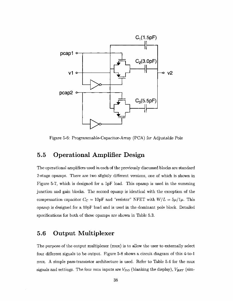
5.4.1 Programmable Capacitor Array (PCA)
The purpose of the programmable capacitor array (PCA) block as shown in Figure
5-6 is to provide a method to externally tune the location of the pole. This is an
important feature of this design. The block uses two external digital signals pcapl &
pcap2 to connect in parallel three different capacitors in four different combinations.
Table 5.2 shows these four selections, the resulting value of Cp in each case, and the
value of the resulting pole with a switch-capacitor clock frequency of fsw = 20kHz.
Combining this digital pole adjustment with f8 ., which allows for a continuous
adjustment over the range [10kHz, 40kHz], results in an externally selectable pole
over a broad range of frequencies: [5Hz, 133Hz].
37
pcap2 pcapl Cp f, (fsw=20kHz)0 0 1.5pF 66.7Hz0 1 4.5pF 22.2Hz1 0 7.OpF 14.3Hz1 1 10.0pF 10.0Hz
C,(1.5pF)
poap 1L o-C2(3.QpF)
V1 o- v2
-C> Tpcap2 1L C3(5.5pF)
Figure 5-6: Programmable-Capacitor-Array (PCA) for Adjustable Pole
5.5 Operational Amplifier Design
The operational amplifiers used in each of the previously discussed blocks are standard
2-stage opamps. There are two slightly different versions, one of which is shown in
Figure 5-7, which is designed for a 1pF load. This opamp is used in the summing
junction and gain blocks. The second opamp is identical with the exception of the
compensation capacitor Cc = 10pF and "resistor" NFET with W/L = 5/11. This
opamp is designed for a 10pF load and is used in the dominant pole block. Detailed
specifications for both of these opamps are shown in Table 5.3.
5.6 Output Multiplexer
The purpose of the output multiplexer (mux) is to allow the user to externally select
four different signals to be output. Figure 5-8 shows a circuit diagram of this 4-to-i
mux. A simple pass-transistor architecture is used. Refer to Table 5.4 for the mux
signals and settings. The four mux inputs are VDD (blanking the display), VBRT (sim-
38

-7
-PU 1 811IL I Y
vinmodc, FPULU TUU kovinp -Lcr,(lpF)
,7--PU
3 C( U)[R
-PU
4?U tu tu
vb3-
vb4oII
ovout
Figure 5-7: Operational Amplifier (1pF load) Circuit Diagram
Table 5.3: Opamp Specifications
Metric 1pF Opamp 10pF Opamp
DC Small Signal Gain 870 870Output Range (V) 0-4.95 0-4.95Unity Gain Frequency (MHz) 1.3 1.0Phase Margin (degrees) 65 55Bias Current (MA) 40 40Power Dissipation (pW) 600 600
39

Table 5.4: Main Channel
ply passing through the input signal),
and VSH (the output of the CSA).
vdd
vbrt
vdrv
vimg
5-8: Output Multiplexer
MUX Settings
VDRV (the output of the Loop Compensator),
40
vout
muxOF-u
mux1i
Figure
MUXi MUXO Signal Mode0 0 VDD Blank Display
0 1 VBRT Feedthrough1 0 VDRV Feedback Drive
1 1 VSH Imaging

Chapter 6
Integrated Silicon Chip Results
6.1 Silicon Chip Overview
The integrated silicon chip which demonstrates the.objectives of this thesis was de-
signed using a Cadence design kit customized for National Semiconductor. The spe-
cific process is a 0.35um 5V process which was chosen for a couple of reasons. Firstly,
high speed was not necessary for this particular application and neither were low
voltages. Therefore a newer submicron process was not used and a 0.35um process
was chosen for its stability. Furthermore, a higher voltage rail was desired in order to
better interface with the organic circuitry. A 20V rail would be ideal, though there
were few National processes with this feature. Instead, a 5V process was chosen with
the intent that an external discrete circuit will be used to bridge the silicon drivers
and the organic inputs. Eventually, as the organic devices improve and their opera-
tional voltages decrease, the external circuit will be removed and the silicon will drive
the organics directly.
A die photo of the fabricated chip is shown in Figure 6-1. The major components
of the chip are highlighted in this photo. There are sixteen main channels which are
intended to drive an equal number of display columns. The current inputs feed in
along the top of the chip. The signals propagate vertically down through the chip
through the Current-Sensing Amplifier blocks followed by the Loop Compensator
blocks. At the bottom of each channel, these signals pass through a bank of output
41

Figure 6-1: Silicon Chip (MITOLEDB) Die Photo
42
multiplexers (muxes). These muxes combine four different signals which can be ex-
ternally selected. Refer to Table 5.4 for the mux signals and settings. The sixteen
outputs of these channels are then split and branch out to the left and right sides of
the chip. The clock drivers on the left side of the chip take one external clock as an
input and generate four clocks with the appropriate timing for the switch-capacitor
circuitry.
A single test channel is located on the bottom part of the chip. The purpose of the
test channel is to characterize each of the individual blocks separately. As a result,
this test channel differs from a single main channel in a few significant ways. The CSA
block is identical with a switch-capacitor gain stage. The Loop Compensator block
only contains one -10x gain stage as it was deemed unnecessary to have two identical
blocks to characterize separately. Furthermore, most of the key intermediate signals
connecting each of the individual blocks were pulled out to pads in order to test these
blocks separately. Unfortunately, this caused problems while testing the test channel,
as these intermediate nodes were not designed to drive such large capacitances. In
most cases, the results from the test channel did not match the main channel, and
often, blocks in the test channel would not function properly at all.
The most commonly observed incorrect behavior in the test channel involved the
block railing one way or another regardless of input voltages. The theory behind
this behavior is that there is an unexpected offset in the inital stages of the test
channel. This offset could be caused by random transistor mismatch or could be
due to a larger than expected input noise level. Since both the CSA and the Loop
Compensator contain blocks with significant gain factors, a small offset upstream
leads to a much larger error downstream, typically resulting in one or more railing
outputs.
6.2 Test Setup
A printed circuit board (PCB) was designed to interface all of the appropriate signals
to the silicon chip for testing purposes. The board provided a way to connect a data
43

acquisition (DAQ) card, up to six BNC cables, and numerous other power and data
signals to the chip. In addition to a personal computer with Labview code which was
briefly used, the test setup included a HP 4156C Semiconductor Parameter Analyzer.
The latter was used to create precise current biases for the chip, and additionally
to run DC sweeps. Finally, a host of function generators and power supplies were
connected to create clock waveforms, sine waveforms, and DC voltages.
While making it easy to connect a large number of signals to the silicon chip,
the PCB actually caused some measurement problems. Due to the large number of
signals lines that were routed on the board, the PCB software autoroute feature was
used. Unfortunately, this led to a maze of wires traversing across and around the
board. Since many of these signals are switching waveforms, this caused a significant
amount of noise and variation on important signal lines. As a result, occasionally the
PCB was bypassed and signals were connected directly to the back of the package,
with mixed results. Future versions of the PCB will be more carefully routed.
6.3 Measurements & Results
As discussed above, there are some inherent problems which are difficult to get around
while testing the test channel. The large capacitive loading of internal nodes modified
the measured results from what the simulations predicted. Additionally, there was
often contention between external and internal circuits both attempting to drive an
intermediate internal node.
The main channel, however, did not suffer from these problems. However, it did
have its own limitations. In order to test the Loop Compensator as a stand alone
block, only one (VBRT) of its two inputs could be driven. In the main channel, the VSH
input is directly driven by the CSA block, and while it can be measured by switching
the output mux to the appropriate setting, it cannot be driven directly. Thus, the
results below were obtained using the following procedure:
1. Set the output mux to the VSH setting (MUX=11). Measure the DC output of
the mux for one channel. This is equivalent to the output of the CSA block for
44

that channel. Record this number and use it to calculate input-referred offset
later.
2. Switch the output mux to the VDRV setting (MUX=10). Drive the VBRT input
corresponding to the same channel with the appropriate waveform. This wave-
form should have its DC value centered around the value obtained in step 1 or
else the output will rail (due to the gain of the Loop Compensator). Measure
and record the output of the mux, which is now equivalent to the output of the
LC block for that channel.
3. Repeat step 2 for all other relevant measurements for this channel.
The assumption that is made in the above procedure is that the measured VSH
value won't change even though it appears that it is not being externally driven. The
justification for this assumption is that while it's not explicitly driven externally, the
CSA block is driving it internally. The CSA input is disconnected, corresponding
to IIN = 0, a valid input signal. While the input-referred offset of the CSA varies
among channels and chips and is unknown at this time (and therefore the CSA output
is unpredictable), it was found to be time invariant. A particular CSA output of a
particular channel of a certain chip remained the same several days later, even if the
test setup was modified. This observation was important, as without it, the following
measurements could not be made.
Table 6.1 shows the important performance metrics of the Loop Compensator
block, and compares the simulated results to the measured results, along with an
associated percent error. Pre-layout simulation results are quoted, as the time it
took to complete some of the post-layout simulations was impractical. The following
sections discuss each of these measurements and explain where any discrepancies
occur.
6.3.1 DC Measurements
In order to determine the open-loop DC gain, input referred offset, input common-
mode range, and output swing, a DC sweep was conducted using the HP 4156C
45

Table 6.1: Loop Compensator Measured and Simulated (Pre-Layout) Results.
Metric Simulated Value Measured Value %-ErrorOpen-Loop DC Gain 99.6 100.18 0.6Open-Loop Pole (PCAP=11) 10.0Hz 10.8Hz 8.0Open-Loop Pole (PCAP=10) 14.3Hz 13.5Hz 5.6Open-Loop Pole (PCAP=01) 22.2Hz 22.8Hz 2.7Open-Loop Pole (PCAP=00) 66.7Hz 64.8Hz 2.8Input-Referred Offset 30mV 49mV N/AInput Common-Mode Range 0-5V 0-5V N/AOutput (VDRV) Swing 0-5V 0.95-4.95V N/A
Semiconductor Parameter Analyzer. This sweep was conducted around the VSH value
for that channel, as described in the step-by-step procedure above. The data from
one particular channel is shown in Figure 6-2.
This data shows an open-loop DC gain of 100.18 and an output swing of [0.95V,
4.95V]. The gain matches very well to the simulated value. The output swing matches
well at the high end but is off by almost 1V at the low end. The initial theory behind
this anomaly was that there was parasitic contention among the various signals driving
the output mux (see Figure 6-3). However, this did not show up in any simulation.
Specifically, in all simulated scenarios, the output of the mux tracked the VDRV input
from rail to rail, with neglible error.
Another theory was that this output voltage could be attributed to a non-zero
GND signal. During testing, it was observed that the GND (and VDD) rail contained
a significant amount of noise at the switching frequency. Due to large current spikes
on the clock edges and finite metal trace resistances, there were significant measured
voltage spikes on the GND rail. Since the banks of dominant pole compensation
blocks and output muxes are physically located near the bottom of the chip, and
the GND pad is located at the top of the chip, there is a significant IR drop across
this GND trace (see Figure 6-4). This metal line can be roughly modeled as a 4.25Q
resistor. With an estimated peak current of 200mA, this results in a local GND
voltage at the main channel output of 0.85V. However, although this is not ideal
behavior, these spikes should only occur on the clock edges and are transient effects.
46
/
131 2.32 2.33 2.34 2.35 2.36 2.37VBRT (V)
Figure 6-2: Loop Compensator Input/Output Characteristics
vdd
vbrt
vdrv
vimg
Figure 6-3: Output Multiplexer
47
2
1
/
//
.7/
y 100. 18x - 231.82R2 = 0.9998-. -- -. --.
('I I I I I2.38
muxO
mux1
- vout

0.582Vclk
0.130 gen0. 544 V
0.13D 1l0.566V gen
0.600V0.410 4
0.656V
0.622V V n0.27f) 0.684V
0.650V gen
0.3401 0. 707V
0.673V gen0.22rl 112 clk0.681 V .7V
0. 715V
0
Figure 6-4:
CSA: Transimpedance Stage I
l T1 _ FI 2.27n_11 r l 1T .40AA ___ _______
0.081V
CSA: Gain Stage
I CSA:I Differential-to-Single Ended
Conversion Stage 2
CSA: Sample and Hold Stage I-
- - - --------- -- - - -
I Summing JunctionI &
Compensator
.567V 12.3rl 0. 149V-J--| L - J. -" w I -J. L
Test Channel:CSA, Summing Junction, & Compensator
Silicon Chip Ground Model [10]
Therefore, it is unlikely that these spikes caused the observed DC error.
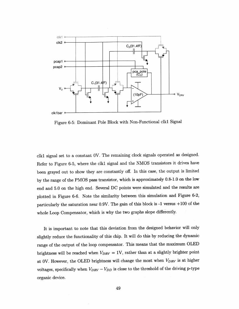
The most likely source of this error is due to incorrect clock signals. During
testing, it was observed that the 4 outputs of the clock generation blocks (clkl, clk2,
clk1bar, and clk2bar) would initally have the desired behavior. This means that clk1
and clk2 would be non-overlapping 20kHz clock signals, while clk1bar and clk2bar
would approximately be their inverses. However, after some testing, often one or
more of the clock signals would deviate from this expected behavior. Typically this
meant that a particular signal would be stuck on one of the rails and would switch no
longer. Occasionally, the signal would still switch, but it would no longer swing from
rail to rail. Once such a problem occurred, the particular clock signal would stay in
this defective mode permanently. The theory is that the testing process caused some
sort of irreversible damage to the chip. The only solution was to begin testing a fresh
chip.
In order to verify that this problem could cause the observed DC error, the fol-
lowing experiment was conducted. The dominant pole block was simulated with the
48
lk1clk2
pcap1
pcap2
V3
ciki bar
0
o
C1(31.4
Figure 6-5: Dominant Pole Block with Non-Functional clk1 Signal
clk1 signal set to a constant OV. The remaining clock signals operated as designed.
Refer to Figure 6-5, where the clk1 signal and the NMOS transistors it drives have
been grayed out to show they are constantly off. In this case, the output is limited
by the range of the PMOS pass transistor, which is approximately 0.8-1.0 on the low
end and 5.0 on the high end. Several DC points were simulated and the results are
plotted in Figure 6-6. Note the similarity between this simulation and Figure 6-2,
particularly the saturation near 0.9V. The gain of this block is -1 versus +100 of the
whole Loop Compensator, which is why the two graphs slope differently.
It is important to note that this deviation from the designed behavior will only
slightly reduce the functionality of this chip. It will do this by reducing the dynamic
range of the output of the loop compensator. This means that the maximum OLED
brightness will be reached when VDRV = 1V, rather than at a slightly brighter point
at OV. However, the OLED brightness will change the most when VDRV is at higher
voltages, specifically when VDRV - VDD is close to the threshold of the driving p-type
organic device.
49
a -
C2(31.4f F)
_pc pole _
F) ~
- (1 0pF) I' VDRV

4
3
2.5
0
2
1.5
o E4.
KK
K.K
KK
KK
KK
KK
0.91
..K...
- ~I I
1 1.5 2 2.5 3 3.5 4 4.5 5V3 (V)
Figure 6-6: DC Sweep Simulation of Dominant Pole Block with clk1 = OV
6.3.2 AC Measurements
Determining the frequency response of the Loop Compensator is critical in assessing
its functionality and performance. For this measurement, a sine wave signal generator
was used to input waveforms at the VBRT input centered around the VSH DC value. In
order to take measurements with reasonable precision, the sine wave was first attenu-
ated using a 10:1 resistive divider. It then passed through the Loop Compensator (a
maximum theoretical gain of 100) and measured at the output. The input amplitude
and DC bias was set such that the circuit was operating in the high-gain linear region
shown in Figure 6-2. Furthermore, the input was set such that the output covered as
close to the full dynamic range of the circuit without clipping. The amplitude of input
and output sine waves were measured across a wide range of relevant frequencies, and
the results plotted in a log-log format. Finally, this procedure was repeated for all
four digital PCAP settings, to determine the locations of the variable pole. These
tests were conducted at a switch-capacitor frequency of 20kHz, and the results are
50
A N.
..... .. .. .
.. .. ..... ......
3.5F

SP00.P01i
+P1o.
--- - . P11
.. .. .... .. .. ... .. .. .. .... O
...... ~ ~ ~ ... .. ... .. .. +-110 -
C -* - , - --:... ...
10 -
10. .
101'. 100 10 102 10 10
Frequency (Hz)
Figure 6-7: Loop Compensator Frequency Characteristics f,, = 20kHz
shown in Figure 6-7.
The results match the simulations well. At each PCAP setting, they show a roll-off
consistent with a single-pole behavior. Furthermore, as the programmable feedback
capacitor value is decreased, the bandwidth of the circuit increases. By calculating
the 3dB points on this graph (rather than extrapolating the unity-gain frequencies,
which can lead to inaccurate results), we can determine the exact location of the
pole. At simulated pole locations of 10.0, 14.3, 22.2, and 66.7 Hz, the percent error
between measured and simulated results is 8.0%, 5.6%, 2.7%, and 2.8%, respectively.
Considering that the individual points in the above figure were obtained by measuring
sine wave amplitudes off of an analog scope, these are very good numbers. The
remaining sub-8.0 percent error can be attributed to inaccuracies in the way the
measurements were taken.
51

6.3.3 Other Measurements
The input-referred offset was calculated by comparing the previously measured value
of VSH with the VBRT voltage that drives the output to 2.5V. By averaging values
from 10 different channels, a value of 49mV was measured. This is fairly close to
the simulated value of 30mV, and below the 50mV specification. In the closed-loop
system, the offset of the LC block corresponds to the error between the VBRT and
VSH signals. An offset less than 50mV corresponds to an error less than 1%, which is
acceptable for this design.
The input common-mode range was determined by looking at data from as many
as 10 different channels on 3 separate chips. This is because the input common-mode
is determined by the uncontrollable VSH input. Channels were found with a VSH
varying from OV to 5V, and DC sweeps were conducted to verify functionality at
these common-mode input voltages. The reason the input of the LC (which is the
summing junction block) has such a wide common-mode range is that the architecture
in this block keeps the op-amp inputs close to VcM, while the actual inputs can vary
over a broader range.
52

Chapter 7
Conclusions
This thesis and associated research presents a novel feedback approach to a prac-
tical problem. This problem is one of producing an OLED display with improved
uniformity and a longer lifetime. First, the organic system was described and mod-
eled. Then. the feedback approach was presented at a higher abstraction level. Next,
a silicon system was specified, designed, fabricated and characterized. The results
were presented and shown in most cases to match the simulated predictions well.
When discrepancies existed, reasoning and simulations were provided regarding their
source(s).
Logically, the next step would be to combine the silicon and organic systems
and demonstrate functionality of an improved display using this closed-loop feedback
technique. However, there are currently a few obstacles to completing this. Primarily,
the organic display is simply not ready at the time of the completion of this thesis.
The integrated organic fabrication process combining OLEDs, OPDs, and OFETs
together in a usable circuit is still being developed, characterized, and improved.
Once this organic display is ready, the feedback loop will be a step closer to being
complete.
The second difficulty involves the Current-Sensing Amplifier (CSA). Much like
the Loop Compensator, the CSA is composed of several distinct circuit blocks. While
each of these blocks functions well as designed individually, when put together suffer
from input-referred offsets. The nature of the block (amplifying currents on the nA
53
level) make it very susceptible to noise and test setup variations, which was observed
constantly throughout testing. If a redesign were to occur, perhaps an architectural
change would be useful here, in order to minimize this block's susceptibility to noise
and offsets.
Furthermore, the key difficulties in characterizing the Loop Compensator and
obtaining measurable and repeatable data were due to non-ideal power rails and
clock signals. In future versions of this chip, additional effort should be taken to
improve these signals. Implementing a ground plane or a full power/ground grid on
metal layers 3 and 4 could mitigate these problems greatly. Additionally, care should
be taken when designing the clock drivers and routing them to the appropriate signal
blocks.
In general, however, the silicon circuits described herein demonstrate the valid-
ity of the feedback approach and their application to improving the uniformity and
lifetime of OLED displays.
54

Bibliography
[1] B. Wei, C. Silva, E. Koutsofios, S. Krishnan, and S. North, "Visualization
Research with Large Displays," Computer Graphics and Applications, IEEE,
vol. 20, no. 4, pp. 50-54, July-Aug 2000.
[2] P. E. Burrows, V. Bulovic, S. R. Forrest, L. S. Sapochak, D. M. McCarty, and
M. E. Thompson, "Reliability and Degradation of Organic Light Emitting De-
vices," Applied Physics Letters, vol. 65, no. 23, pp. 2922-2924, December 1994.
[3] E. T. Lisuwandi, "Feedback Circuit for Organic LED Active-Matrix Display
Drivers," Master's thesis, Massachusetts Institute of Technology, 2002.
[4] M. R. Powell, "Integrated Feedback Circuit for Organic LED Display Driver,"
Master's thesis, Massachusetts Institute of Technology, Mar. 2004.
[5] C. Adachi, M. A. Baldo, and S. R. Forrest, "High-Efficiency Organic Electrophos-
phorescent Devices with tris(2-phenylpyridine)Iridium doped into Electron-
Transporting Materials," Applied Physics Letters, vol. 77, no. 6, pp. 904-906,
August 2000.
[6] J. J. Yu, "A Smart Active Matrix Pixelated OLED Display," Master's thesis,
Massachusetts Institute of Technology, Jan. 2004.
[7] H. Antoniadis, "Overview of OLED Display Technology,"
http://www.ewh.ieee.org/soc/cpmt/presentations/cpmt0401a.pdf.
[8] C. W. Tang and S. A. VanSlyke, "Organic Electroluminescent Diodes," Applied
Physics Letters, vol. 51, no. 12, pp. 913-915, September 1987.
55

[9] G. B. Levy, W. Evans, J. Ebner, P. Farrell, M. Hufford, B. H. Allison,
D. Wheeler, H. Lin, 0. Prache, and E. Naviasky, "An 852x600 Pixel OLED-on-
Silicon Color Microdisplay using CMOS Sub-threshold-Voltage-Scaling Current
Drivers," IEEE Journal of Solid-State Circuits, vol. 37, no. 12, December 2002.
[10] A. Lin, "A Silicon Current Sensing Amplifier and Organic Imager for an Optical
Feedback OLED Display," Master's thesis, Massachusetts Institute of Technol-
ogy, Jan. 2006.
[11] D. E. Johns and K. Martin, Analog Integrated Circuit Design. John Wiley &
Sons, Inc., 1997.
56