an investigation of electroelastic bandgap formation in
TRANSCRIPT

An investigation of electroelastic bandgapformation in locally resonant piezoelectricmetastructures
C Sugino1, S Leadenham1, M Ruzzene1,2 and A Erturk1
1G.W. Woodruff School of Mechanical Engineering, Georgia Institute of Technology, Atlanta, GA, UnitedStates of America2D. Guggenheim School of Aerospace Engineering, Georgia Institute of Technology, Atlanta, GA, UnitedStates of America
E-mail: [email protected]
Received 23 December 2016, revised 23 February 2017Accepted for publication 13 March 2017Published 19 April 2017
AbstractLocally resonant electromechanical metastructures made from flexible substrates withpiezoelectric layers connected to resonant shunt circuits exhibit vibration attenuation propertiessimilar to those of purely mechanical metastructures. Thus, in analogy, these locally resonantelectromechanical metastructures can exhibit electroelastic bandgaps at wavelengths much largerthan the lattice size. In order to effectively design such metastructures, the modal behavior of thefinite structure with given boundary conditions must be reconciled with the electromechanicalbehavior of the piezoelectric layers and shunt circuits. To this end, we develop the theory for apiezoelectric bimorph beam with segmented electrodes under transverse vibrations, and extractanalytical results for bandgap estimation using modal analysis. Under the assumption of aninfinite number of segmented electrodes, the locally resonant bandgap is estimated in closedform and shown to depend only on the target frequency and the system-level electromechanicalcoupling. It is shown that bandgap formation in piezoelectric metastructures is associated with afrequency-dependent modal stiffness, unlike the frequency-dependent modal mass in mechanicalmetastructures. The relevant electromechanical coupling term and the normalized bandgap sizeare calculated for a representative structure and a selection of piezoelectric ceramics and singlecrystals, revealing that single crystals (e.g. PMN-PT) result in significantly wider bandgap thanceramics (e.g. PZT-5A). Numerical studies are performed to demonstrate that the closed-formbandgap expression derived in this work holds for a finite number of electrode segments. It isshown that the number of electrodes required to create the bandgap increases as the targetfrequency is increased.
Keywords: metamaterials, metastructures, piezoelectricity, vibration, bandgap, damping,electromechanical
(Some figures may appear in colour only in the online journal)
1. Introduction
Piezoelectric shunt damping has been studied for many yearsas an effective way to reduce structural vibrations of light-weight and flexible structures without significant mass addi-tion, one of the typical problems with conventional, purelymechanical damping techniques [1, 2]. Using piezoelectricity,energy is transferred from the mechanical to electrical
domain, where it can be dissipated or stored [3, 4]. Thisintroduces significant design freedom, since electrical energycan be manipulated by any combination of commonly avail-able analog and digital electrical components. Forward [5]first proposed shunt damping using negative feedback andtwo piezoelectric patches, one acting as a sensor and the otheras actuator. Hagood and von Flotow [6] showed that a singlepiezoelectric patch using an inductive shunt circuit acts as a
Smart Materials and Structures
Smart Mater. Struct. 26 (2017) 055029 (10pp) https://doi.org/10.1088/1361-665X/aa6671
0964-1726/17/055029+10$33.00 © 2017 IOP Publishing Ltd Printed in the UK1
mechanical resonator, yielding an electromechanical versionof the well-known dynamic vibratrion absorber effect [7].Others have demonstrated multi-modal damping performanceusing more complex networks of resonant circuits [8, 9], orused negative capacitance shunting to achieve vibrationreduction [10–12]. Various nonlinear switching circuitshave also been shown to be effective for vibration reduction[14–16], although they introduce additional complexity.
More recently, shunt damping techniques have beenemployed in conjunction with locally resonant metamaterialconcepts, using many piezoelectric elements on a structure tocreate bandgaps, or frequency ranges in which vibrationdisturbances will not propagate through the structure. Inanalogy with structures using many mechanical resonators[17, 18], structures employing many resonant shunt circuitscan display ‘locally resonant’ bandgaps at wavelengths muchlarger than the lattice size [19–23], enabling the formation oflow-frequency bandgaps in structures for wideband vibrationand/or sound attenuation.
Typical approaches for modeling metamaterials assumean infinite or a semi-infinite structure made from a repeatedunit cell, allowing the use of the Bloch theorem to obtain theband structure of the material. However, for practical imple-mentation, it is necessary to understand the performance offinite size metamaterial-based electromechanical structures,i.e. electromechanical metastructures, and how the modeshapes of the structure interact with the shunt circuits. To thisend, we present a distributed-parameter electromechanicalmodel and modal analysis of a one-dimensional locallyresonant thin metastructure under transverse vibrations. Firstthe generalized segmented electrode formulation is reviewedfor a finite number of shunts. Then, based on the assumptionof an infinite number of segmented electrodes, the response ofthe beam is derived in closed form, and it is shown that theshunt circuitry admittance adds frequency-dependence to thestiffness of the structure. By assuming ideal resonant shunt-ing, with each circuit tuned to the same resonant frequency,the locally resonant bandgap edge frequencies are derived inclosed form. The bandgap edge frequencies depend only onthe resonant frequency of the shunt circuits and the system-level electromechanical coupling. The coupling parameterdepends on the geometry of the bimorph and the properties ofthe piezoelectric layers. For comparison, the expected elec-tromechanical coupling is calculated for a variety of piezo-electric ceramics and single crystals. Numerical studies areperformed for a bimorph cantilever with a finite number ofsegmented electrodes to validate the analytical bandgapestimation.
2. Modal analysis of electroelastic bandgapformation
Consider a bimorph piezoelectric beam with rectangular crosssection made from two continuous and symmetrically locatedpiezoelectric layers sandwiching a central structural (i.e. shimor substrate) layer (figure 1). The piezoelectric layers areoppositely poled in thickness direction and the inner
electrodes are combined with each other (through the con-ductive substrate), yielding series connection under transversevibrations, while parallel connection is also possible byproperly insulating and combining the respective electrodes.The outer surface electrodes are segmented as pairs andconnected to a total of S shunt circuits. The electrode layersand the bonding layers are assumed to have negligiblethickness. The thin composite beam has certain specifiedboundary conditions and is modeled based on the Euler–Bernoulli beam theory by assuming geometrically smalloscillations and linear-elastic material behavior. For simpli-city, the beam is assumed to be undamped, with the under-standing that modal damping can be added easily.
Under the excitation of a distributed transverse force perunit length ( )f x t, (acting in z-direction in the xz-plane), thegoverning electromechanical equations for linear bendingvibrations of the beam and current balance in shunt circuitsare
åJ¶¶
+¶¶
-
´ - - - ==
( )
[ ( ) ( )] ( ) ( )
EIw
xm
w
tv t
x
H x x H x x f x t
d
d
, , 1
j
S
j
jL
jR
4
4
2
21
2
2
òJ+ +¶¶ 
= = ¼( )
( )
Cv
tY v t
w
x tx j S
d
dd 0, 1, , ,
2
p jj
j jx
x
,
3
2jL
jR
where ( )w x t, is the transverse displacement of the beam atposition x and time t; vj(t) and Yj are, respectively, the voltageand the external load admittance across the jth electrode pair,and H(x) is the Heaviside function. Furthermore, EI is theshort-circuit flexural rigidity, m is the mass per length, ϑ is theelectromechanical coupling term in physical coordinates, andCp j, is the internal piezoelectric capacitance across the jthelectrode pair, given by
= + + -⎜ ⎟⎛⎝⎜⎜
⎡⎣⎢
⎛⎝
⎞⎠
⎤⎦⎥
⎞⎠⎟⎟¯ ( )EI
bc
hc h
h h2
3 8 2 8, 3s
s Ep
s s3
11
3 3
Figure 1. Schematic of a piezoelectric metastructure and a close upshowing the jth electrode pair shunted to an electrical load ofadmittance Yj. Since periodicity is not required, the electrode pairsdo not have to be identical. Symmetrically located piezoelectriclayers are connected in series for transvervse vibrations (polingdirections are shown by gray arrows).
2
Smart Mater. Struct. 26 (2017) 055029 C Sugino et al

r r= +( ) ( )m b h h2 , 4s s p p
J = + -⎜ ⎟⎡⎣⎢
⎛⎝
⎞⎠
⎤⎦⎥
¯ ( )e b
hh
h h
2 2 4, 5e
pp
s s312 2
e=-
¯( )
( )C bx x
h2. 6p j
Se
jR
jL
p, 33
Here, cs, rs, and hs are the central substrate layer’s elasticmodulus, mass density, and thickness, respectively, while b isthe width of the beam. The piezoelectric layers have massdensity rp, thickness hp, width b, elastic modulus at constant
electric field cE11, effective piezoelectric stress constant e31, and
permittivity component at constant strain e S33, where the
overbars indicate effective material properties for 1D thinlayers reduced from 3D constitutive equations as
e e= = = -¯ ¯ ¯ ( )cs
ed
s
d
s
1, , , 7E
E ES T
E1111
3131
1133 33
312
11
where s11E is the elastic compliance at constant electric field,
d31 is the piezoelectric strain constant, and eT33 is the permit-
tivity component at constant strain. The piezoelectric layershave segmented surface electrodes numbered = ¼j S1 ,with each electrode starting at =x xj
L and ending at xjR, with
total length D = -x x xj jR
jL (figure 1), and width be, sym-
metric about the xz-plane.Using an assumed-modes type expansion with N number
of modes, the transverse displacement of the beam can begiven by
åf h==
( ) ( ) ( ) ( )w x t x t, , 8r
N
r r1
where h ( )tr are the modal weightings to be determined. Themode shapes f ( )xr of the beam obtained for a given set ofmechanical boundary conditions (at short circuit) are nor-malized such that
ò f f d= = ¼( ) ( ) ( )m x x r s, , 1, 2, , 9L
r s rs0
ò ff
w d= = ¼( ) ( )EI xx
x r sd
dd , , 1, 2, , 10
L
rs
r rs0
4
42
where L is the length of the beam, wr is the rth natural fre-quency, and drs is the Kronecker delta. Note that equation (10)can be written in symmetric form
òf f
w d= = ( )EIx x
x r sd
d
d
dd , , 1, 2 ,.... 11
Lr s
r rs0
2
2
2
22
Substituting equation (8) into equation (1), multiplyingby some mode shape f ( )xk , and integrating across the beam(see [24] for a full derivation with a single electrode, whichcan be easily extended to multiple electrodes), governingequations can be obtained in modal coordinates as
åh w h J f+ - D ¢ ==
( ) ( ) ( ) ( ) ( )t t v t q t¨ , 12r r rj
S
j r j r2
1,
åJ f h+ + D ¢ ==
( ) ( ) ( ) ( )C v t Y v t t 0, 13p j j j jr
N
r j r,1
,
where the free indices r and j are assumed to go from ¼ N1and ¼ S1 , respectively,
ff f f
D ¢ = = -⎛⎝⎜
⎞⎠⎟ ( ) ( ) ( )
x xx
xx
d
d
d
d
d
d14r j
r
x
xr
jR r
jL
,jL
jR
is the difference in slope of the rth mode between the ends ofthe jth electrode and
ò f=( ) ( ) ( ) ( )q t f x t x x, d 15r
L
r0
is the modal forcing. Taking the Laplace transforms ofequations (12) and (13), we can obtain separate equationsgoverning the modal weightings and voltages,
å
å
w Jf
f
+ +D ¢
+
´ D ¢ =
=
=
( ) ( )( )
( ) ( ) ( )
s H s ssC Y s
H s Q s , 16
r rj
Sr j
p j j
k
N
k j k r
2 2 2
1
,
,
1,
å
å
Jf
w
f
+ +D ¢
+
´ D ¢ =
=
=
( ( )) ( )
( ) ( ) ( )
sC Y s V s ss
V s Q s . 17
p j j jr
Nr j
r
k
S
r k k j
,2
1
,
2 2
1,
Focusing on the modal weightings, equation (16) can bewritten as
å
å
wa f
f
+ ++
D ¢
D
´D ¢
DD =
=
=
( ) ( )( )
( ) ( ) ( )
s H ss
s h sEI
x
xx H s Q s , 18
r rj
Sr j
j
k
Nk j
jj k r
2 2
1
,
1
,
where
aJ
e e= =
+
¯¯ ( )
¯( )
h
EI b
e b h h h
EI
2
219
p
Se
e p s p
S
2
33
312 2
33
is a dimensionless parameter related to the electromechanicalcoupling, and
=( )( )
( )h sY s
C20
j
p j,
is the normalized circuit admittance, which is assumed to beidentical for every electrode pair. The system of equationsdescribed by equation (18) cannot be readily solved for asimple analytical expression for the modal weightings Hr(s)due to the coupling from the presence of the segmentedelectrodes (a matrix inversion solution is suitable in thegeneralized segmented electrode case). However, as an elec-trode pair becomes infinitesimally long,
f fD ¢
D=
D ( ) ( )
x xxlim
d
d, 21
x
r j
j
rj
0
,2
2j
where = =x x xj jL
jR is the x-coordinate of the infinitesimal
electrode. In the limit as all of the electrodes become infini-tesimal and as ¥S ,
3
Smart Mater. Struct. 26 (2017) 055029 C Sugino et al

ò
å å
å
f f
f fw
D ¢
D
D ¢
DD
= =
¥D = =
=
( )
( ) ( ) ( )
EIx x
x H s
EIx x
xH s H s
lim lim
d
d
d
dd . 22
S x j
Sr j
j k
Nk j
jj k
Lr
k
Nk
k r r
0 1
,
1
,
0
2
21
2
22
j
Although this simplification is only exact in the limiting case,it can serve as a good approximation for a finite number ofelectrodes, as will be discussed in later. Equation (18) thenbecomes
wa
w+ ++
=( ) ( )( )
( ) ( ) ( )s H ss
s h sH s Q s . 23r r r r r
2 2 2
Since the system of equations is now decoupled, the modalresponse can be explicitly calculated as
w=
+ + a+( )( ) ( ) ( )
( )
H sQ s
s 1. 24r
r
rs
s h s2 2
From this analysis, it is clear that the presence of the piezo-electric material and segmented electrodes with identicalcircuitry results in a frequency-dependent dynamic modalstiffness, given by
a= +
+( )
( )( )K s
K
s
s h s1 , 25
SC
where KSC is the modal stiffness of the system at short circuit.This is fundamentally different from the purely mechanicallocally resonant counterparts, which results in a frequencydependent dynamic modal mass [18]. Furthermore, whereaswith mechanical resonators the type of expected frequencydependence is limited to various combinations of mass-spring-damper systems, h(s) is associated with the shunt cir-cuit impedance, which greatly expands the design space, e.g.by using generalized synthetic impedance circuits via digitalsignal processing [25].
3. Electromechanical coupling
The key dimensionless parameter α emerges from this ana-lysis, which measures how strongly coupled the piezoelectric
material is to the plain beam, directly affecting how stronglythe shunt circuitry is able to affect the structure. To gain moreintuition on what material properties influence α, substitutingequation (3) into equation (19) yields
ae
=+
+ + +
¯ ( )¯ ( ¯ ( ))
( )b e h h h
b c h c h h h h h
6
2 4 6 3. 26
e p p s
Ss s
Ep p p s s
312 2
333
112 2
Define the dimensionless parameters
g be
= = = =ˆ ˆ¯
¯¯ ¯
( )hh
hb
b
b
c
c
e
c, , , . 27
p
s
e sE E S
11
312
11 33
Then,
ab
g=
+
+ + +
ˆ ˆ ( ˆ )ˆ ( ˆ ˆ )
( )b h h
h h h
6 1
2 4 6 3. 28
2
2
The coupling increases with the width of the electrodes andthe material parameter β. The maximum value of α, assumingfixed β and b, depends only on h, given by
ab
=+ ++
( ˆ)ˆ ( ˆ)( ˆ)
( ˆ)( )h
b h h
h
1 1 3
1 229max 2
which occurs at g = +ˆ ( ˆ)h h4 1 33 (these expressions can be
rearranged to find the optimal h at a certain γ, and equiva-lently a g( )max ). Thus, the maximum value across the entireparameter space is
a be
= = =-
¯¯ ¯
( )e
c
k
k1, 30
E Smax312
11 33
312
312
where
e= ( )k
d
s31
E T312 31
2
11 33
is the standard definition for the piezoelectric material’selectromechanical coupling coefficient. The electro-mechanical coupling α is plotted against h and γ in figure 2,along with h–γ combinations (dashed line) for which α is amaximum. For a fixed piezoelectric material and electrodewidth, the dashed line in figure 2 can therefore be used toselect the optimal thickness ratio given the elastic moduliratio, or vice versa.
In order to give a sense of the typical values of α, consider abimorph cantilever with an aluminum substrate, with =hs
0.1 mm, =c 69 GPas , r = -2700 kg ms3, =L 100 mm, and
=b 10 mm. For the piezoelectric layers, we will consider arepresentative set of piezoelectric materials, all with =hp
0.3 mm and = =b b 10 mme . The relevant material propertiesand corresponding dimensionless parameters for the differentpiezoelectric materials are shown in table 1. Single crystals arealso included in this analysis due to their significantly largerelectromechanical coupling and elastic compliance. PZT-5A andPZT-5H are both commonly used piezoelectric ceramics,whereas PZN-PT, PMN-PT, and PIN-PMN-PT are singlecrystals. Regarding the single crystals, the table contians PZN-PT and PMN-PT data for various % content of PT, while thePIN-PMN-PT considered here has the composition of 27% PIN,40% PMN, and 33% PT [26–28]. Since the single crystals have
Figure 2. Dimensionless electromechanical coupling α normalizedby its maximum value versus normalized piezoelectric thickness hand stiffness ratio γ. The dashed line shows the location of themaximum value of α for a given h or γ value.
4
Smart Mater. Struct. 26 (2017) 055029 C Sugino et al

lower elastic moduli and higher coupling coefficient than thepiezoceramics, they give much larger values of α.
The electromechanical coupling α is also related to theamount of stiffness gained at open circuit, which can be seensimply by setting =( )h s 0, yielding
a= +( ) ( )K s
K1 32
SC
indicating that the effective modal stiffness is increased by afactor of a+1 from short circuit to open circuit. This pro-vides a simple way to estimate α by using
aww
= -⎛⎝⎜
⎞⎠⎟ ( )1, 33i
i
OC,
SC,
2
where w iOC, and w iSC, are the ith natural frequencies at openand short circuit, respectively (which roughly are the ith open-and short-circuit resonant frequencies in a typical lightlydamped system). Therefore, α is related to the couplingcoefficient of the system, i.e. the overall composite structure(which should not be confused with the coupling coefficientof the active material alone, given by equation (31)). Adynamic definition of the system-level electromechanicalcoupling coefficient ki for the ith mode is [29]
w w
w=
-( )k 34i
i i
i
2 OC,2
SC,2
OC,2
which generally depends on the mode under considerationand the electrode configuration. Using the approximation ofan infinite number of electrodes, the coupling coefficientbecomes the same for every mode, given by
aa
=+¥ ( )k
1. 352
It is useful to note that, substituting the maximum value amax
from equation (30) into equation (35), we find that the max-imum value of ¥k 2 is given by
aa
=+
=¥( ) ( )k k1
362max
max
max312
implying that the system’s coupling coefficient converges to theactive material’s coupling coefficient for infinitely many elec-trode segments and under the aforementioned amax condition, asan upper limit. To demonstrate the convergence of the electro-mechanical coupling as the number of electrodes becomes large,consider a uniform bimorph cantilever beam with S evenly
distributed electrodes, such that = -( )x j L S1jL and =xj
R
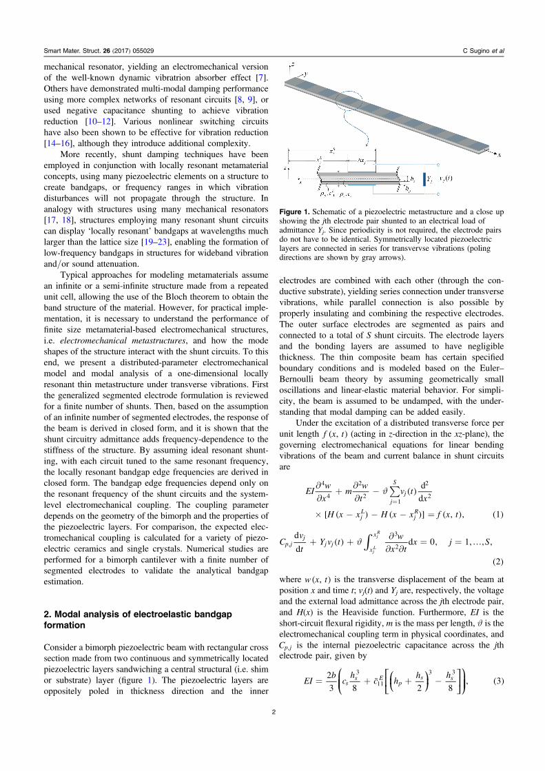
jL S. With that assumption, k2i can be calculated for each modeby comparing open- and short-circuit natural frequencies atvarious values of S, which is shown in figure 3. As S becomeslarge, the coupling approaches ¥k 2 , converging more quickly forlower modes.
It is worth noting that the value of α can be effectivelyincreased by using negative capacitance shunting [13]. Thiscan be seen explicitly by using
= - + -( ) ( ) ( ) ( )h s cs c g s1 , 37
where g(s) is the normalized admittance of a shunt circuitdesigned in the absence of negative capacitance shunting, and< <c0 1 represents the fraction of the piezoelectric capa-
citance being canceled. The response is then
w=
+ + a- + -( )( ) ( ) ( )
( ) ( )
H sQ s
s 138r
r
rs
s cs c g s2 2
1
w=
+ + a+( )
( ) ( )( )
Q s
s 1, 39r
rs
s g s2 2 nc
where
aa
=-
( )c1
40nc
is the effective dimensionless electromechanical coupling inthe presence of negative capacitance shunting. Note that,although equation (40) suggests that anc can be made arbi-trarily large, there are practical limitations preventing suchdesigns, such as the required input power, electrical losses,and stability issues in the circuit.
4. Root locus interpretation of modal response
By rewriting equation (24), the transfer function for the rthvibration mode can be obtained as
w=
+ + a+( )
( )( )
( )( )
H s
Q s s
1
1. 41r
rr
s
s h s2 2
The poles and zeros of this expression give a great deal ofinformation about the structure’s response. Zeros correspondto frequencies where a particular mode shows no response,and poles correspond to resonances of a particular mode. Forthis purpose, it is useful to interpret the transfer function as
Table 1. Typical properties for selected piezoelectric ceramic and single crystal materials [26–28] and corresponding dimensionlessparameters defined in this work (for =c 69 GPas , r = -2700 kg ms
3, =h 0.1 mms , =h 0.3 mmp , =L 100 mm, and = =b b 10 mme ).
Material rs (- )kg m 3 cE
11 ( )GPa e31 ( - )C m 2 S33 ( - )nF m 1 β γ α
PZT-5A 7750 61 −12.3 13.3 0.19 1.13 0.16PZT-5H 7500 60.6 −16.6 25.6 0.18 1.14 0.15PZN-PT (4.5% PT) 8310 12.2 −11.8 34.6 0.33 5.65 0.27PZN-PT (8% PT) 8315 11.5 −16.7 43.8 0.56 5.99 0.46PMN-PT (30% PT) 8040 19.2 −17.7 52.7 0.31 3.58 0.26PMN-PT (33% PT) 8060 14.5 −19.3 47.0 0.55 4.75 0.45PIN-PMN-PT 8198 13.2 −17.7 40.5 0.59 5.20 0.49
5
Smart Mater. Struct. 26 (2017) 055029 C Sugino et al
the closed-loop transfer function of a feedback control sys-tem, with plant and feedback transfer functions
=( ) ( )G ss
1, 42
2
a= +
+( )
( )( )F s
s
s h s1 43
with proportional gain w=K r2. Thus, we consider the poles
and zeros of the system
a= +
+
⎛⎝⎜
⎞⎠⎟( ) ( )
( )( )G s F s
s
s
s h s
11 44
2
a=
+ ++
( ) ( )( ( ))
( )s h s
s s h s
1. 45
2
Simply by considering the poles and zeros of this expressionfor a given h(s), the effect of increasing wr
2 on the poles(resonances) of the system can be inferred using well-knownroot locus analysis [30]. This gives a quick way to determinewhere the resonances of the system are moved by the additionof the segmented shunt circuits, which makes it immediatelyclear if there is a bandgap present, as will be demonstrated forthe simplest form of the locally resonant bandgap.
5. Estimation of electroelastic bandgap size
Although the general framework in the previous sectionallows the analysis of any type of linear shunt circuit, oneinteresting example is the locally resonant bandgap that formsfrom inductive shunting. To obtain the locally resonantbandgap, assume that the circuit impedance is due to an ideal(lossless) inductor, such that
w= =( ) ( ) ( )Y s
L sh s
s
1, , 46j
j
t2
where Lj is the inductance applied to the jth shunt (not to beconfused with the beam length L), and
w = ( )L C
1. 47t
j p j
2
,
Then,
w=
+ + aw+( )
( )( )
( )H s
Q s s
1
1. 48r
rr
s
s2 2
t
2
2 2
Note that as ws j t, ( ) ( )H s Q s 0r r , an antiresonance ispresent for every mode. This is the continuous system analogto a perfectly tuned vibration absorber. Using the previouslymentioned root locus interpretation of the modal response, thesystem transfer function is
a ww
=+ +
+( ) ( ) ( )
( )( )G s F s
s
s s
1. 49t
t
2 2
2 2 2
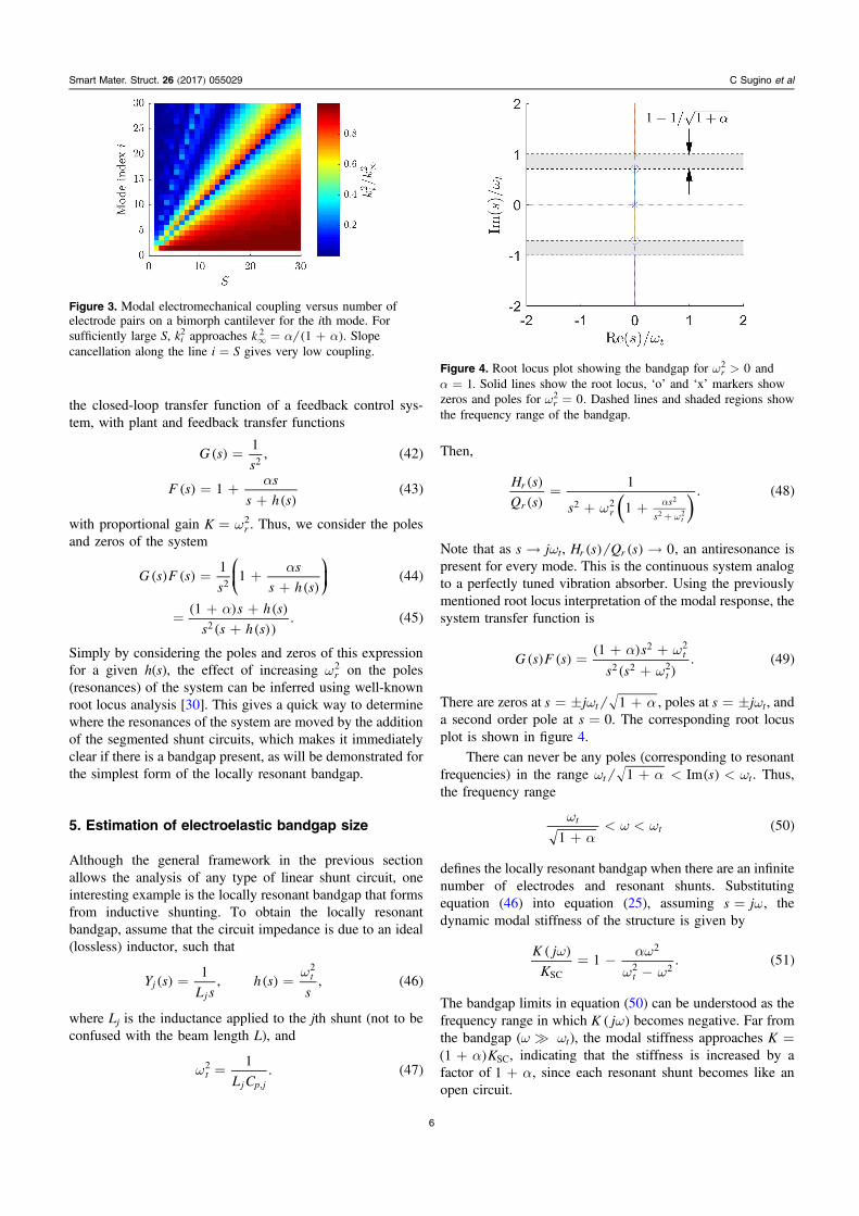
There are zeros at w a= +s j 1t , poles at w= s j t, anda second order pole at s=0. The corresponding root locusplot is shown in figure 4.
There can never be any poles (corresponding to resonantfrequencies) in the range w a w+ < <( )s1 Imt t. Thus,the frequency range
wa
w w+
< < ( )1
50tt
defines the locally resonant bandgap when there are an infinitenumber of electrodes and resonant shunts. Substitutingequation (46) into equation (25), assuming w=s j , thedynamic modal stiffness of the structure is given by
w aww w
= --
( ) ( )K j
K1 . 51
tSC
2
2 2
The bandgap limits in equation (50) can be understood as thefrequency range in which w( )K j becomes negative. Far fromthe bandgap (w w t), the modal stiffness approaches =K
a+( )K1 SC, indicating that the stiffness is increased by afactor of a+1 , since each resonant shunt becomes like anopen circuit.
Figure 4. Root locus plot showing the bandgap for w > 0r2 and
a = 1. Solid lines show the root locus, ‘o’ and ‘x’ markers showzeros and poles for w = 0r
2 . Dashed lines and shaded regions showthe frequency range of the bandgap.
Figure 3. Modal electromechanical coupling versus number ofelectrode pairs on a bimorph cantilever for the ith mode. Forsufficiently large S, ki
2 approaches a a= +¥ ( )k 12 . Slopecancellation along the line i=S gives very low coupling.
6
Smart Mater. Struct. 26 (2017) 055029 C Sugino et al

The bandwidth of vibration attenuation of the locallyresonant bandgap is
w wa
D = -+
⎛⎝⎜
⎞⎠⎟ ( )1
1
1. 52t
For reference, the expected bandwidth as a percentage of thetarget frequency wt is shown in table 2 for the materials fromtable 1 using the same geometric parameters. Note that forboth PZT-5A and PZT-5H, the bandgap is expected to be asmall fraction of the target frequency, whereas some of thesingle crystals are approaching 20% bandwidth.
To center the bandgap at some center frequency wc, thetarget frequency should be selected as
ww a
a=
++ +
( )2 1
1 1. 53t
c
Note that, with an infinite number of electrodes, the bandgapedge frequencies have no dependence on the boundary con-ditions of the beam or the type of excitation. In addition, thebandgap is asymmetric about the target frequency, but in theopposite direction (i.e. below the target frequency, rather thanabove) as the mechanical resonator mass-based bandgaprecently analyzed with a similar approach [18].
The bandwidth of the locally resonant bandgap increasesif negative capacitance is used in addition to resonantshunting. Substituting equation (40) into equation (52) givesthe bandgap bandwidth as
w wa
D = --
- +
⎛⎝⎜
⎞⎠⎟ ( )c
c1
1
1. 54t
The dimensionless bandwidth w wD t, i.e. the bandwidth ofthe bandgap normalized by the target frequency, is shown as afunction of fractional negative capacitance c in figure 5 forconstant α.
A typical way to measure the response of the structure istransmissibility, defined as the ratio of displacements at someoutput location xout to some input location xin, i.e.
åw
f w
f w= =
å =
=
( ) ( )( )
( ) ( )
( ) ( )( )w x
w x
x H j
x H jTR . 55r
Nr r
r
Nr r
out
in
1 out
1 in
With a closed form expression for Hr(s), equation (55)becomes simple to evaluate for very large N. Consider the pre-viously discussed bimorph cantilever with =c 69 GPas , r =s
-2700 kg m 3, =h 0.1 mms , =h 0.3 mmp , =L 100 mm, and= =b b 10 mme (and let PMN-PT with 33% PT be the
piezoelectric material). This structure has clamped-free boundaryconditions (clamped at x= 0 and free at x= L). Let the output bethe transverse displacement at the tip (x= L). Rather than lookingat a particular excitation point, the input location xin can beallowed to vary along with frequency, giving a full picture of thebeam’s response, as shown in figure 6. The resulting bandgap inthis figure agrees with the bandgap size approximation in table 2based on equation (52).
6. Finite number of electrodes and validation ofbandgap size
The simplifications in our analysis thus far rely on theassumption of an infinite number of segmented electrodes.For practical design purposes, it is necessary to understandhow the system behaves with a finite number of electrodepairs and determine how many electrodes are necessary for atarget frequency neighborhood. For the infinite-electrodeapproximation to be used in case of a finite number of elec-trodes, the key approximation is
òåf f f f
w dD ¢
D
D ¢
DD » =
=
( )EIx x
x EIx x
xd
d
d
dd . 56
j
Sr j
j
k j
jj
Lr k
r rk1
, ,
0
2
2
2
22
Using equations (12) and (13), it is simple to obtain thestructure’s response and approximate natural frequenciesusing typical multi-degree-of-freedom dynamical systemstechniques. To check the convergence to the expected infi-nite-electrodes behavior as ¥S , we assume that theelectrodes have uniform length D =x L Sj , covering theentire structure, such that = -( )x j L S1j
L and =x jL SjR .
The electrode pattern is then determined by S only, and theresonant frequencies can be obtained at each value of S.Similarly, the deformed shape of the beam under harmonicbase excitation can be obtained at each S. The resulting
Figure 5. Dimensionless bandgap bandwidth versus fractionalnegative capacitance for a = 0.45. Note that the maximumbandwidth is w wD = 1t , since the upper edge frequency of thebandgap is fixed at wt .
Table 2. Bandgap width as a percentage of target frequency forselected piezoelectric materials (for =c 69 GPas , r = -2700 kg ms
3,=h 0.1 mms , =h 0.3 mmp , =L 100 mm, and = =b b 10 mme ).
Material w wD t (%)
PZT-5A 7.01PZT-5H 6.71PZN-PT (4.5%) 11.44PZN-PT (8%) 17.22PMN-PT (30%) 10.83PMN-PT (33%) 17.070.27PIN-0.40PMN-0.33PT 17.95
7
Smart Mater. Struct. 26 (2017) 055029 C Sugino et al

Figure 7. Transmissibility and resonant frequencies versus S for (a) PZT-5A (a = 0.16), (b) PZN-PT (4.5%) (a = 0.27), (c) PMN-PT (33%)(a = 0.45) for a uniform bimorph cantilever beam excited by base motion, w w= 100t 1, N=200. Small circles indicate resonantfrequencies, heatmap shows transmissibility, dashed lines show the expected bandgap edge frequencies from equation (50), and solid linestrack w +S 1 and wS.
Figure 6. Tip transmissibility ∣ ( ) ( )∣w L w xin versus input location and excitation frequency for a bimorph cantilever beam with a harmonicpoint force excitation at xin bearing an infinite number of segmented electrodes, a = 0.45 (PMN-PT 33%), w w= 50t 1, N=300.
8
Smart Mater. Struct. 26 (2017) 055029 C Sugino et al
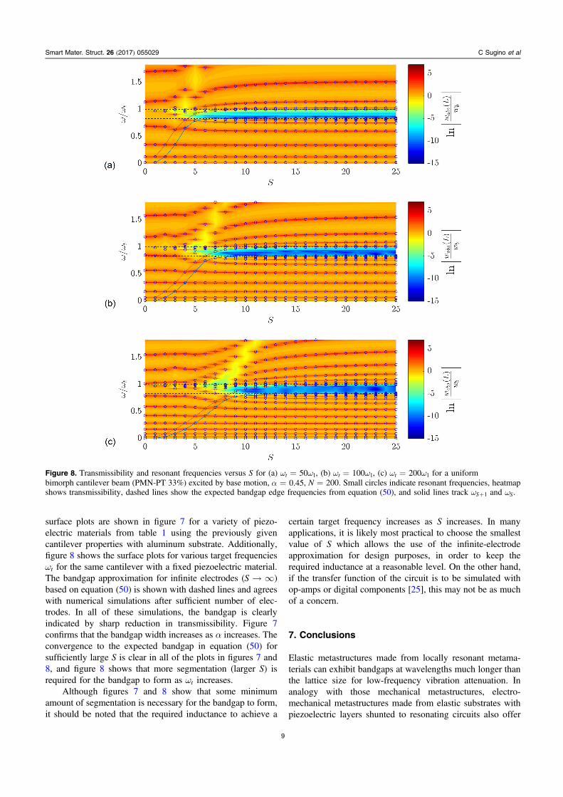
surface plots are shown in figure 7 for a variety of piezo-electric materials from table 1 using the previously givencantilever properties with aluminum substrate. Additionally,figure 8 shows the surface plots for various target frequencieswt for the same cantilever with a fixed piezoelectric material.The bandgap approximation for infinite electrodes ( ¥S )based on equation (50) is shown with dashed lines and agreeswith numerical simulations after sufficient number of elec-trodes. In all of these simulations, the bandgap is clearlyindicated by sharp reduction in transmissibility. Figure 7confirms that the bandgap width increases as α increases. Theconvergence to the expected bandgap in equation (50) forsufficiently large S is clear in all of the plots in figures 7 and8, and figure 8 shows that more segmentation (larger S) isrequired for the bandgap to form as wt increases.
Although figures 7 and 8 show that some minimumamount of segmentation is necessary for the bandgap to form,it should be noted that the required inductance to achieve a
certain target frequency increases as S increases. In manyapplications, it is likely most practical to choose the smallestvalue of S which allows the use of the infinite-electrodeapproximation for design purposes, in order to keep therequired inductance at a reasonable level. On the other hand,if the transfer function of the circuit is to be simulated withop-amps or digital components [25], this may not be as muchof a concern.
7. Conclusions
Elastic metastructures made from locally resonant metama-terials can exhibit bandgaps at wavelengths much longer thanthe lattice size for low-frequency vibration attenuation. Inanalogy with those mechanical metastructures, electro-mechanical metastructures made from elastic substrates withpiezoelectric layers shunted to resonating circuits also offer
Figure 8. Transmissibility and resonant frequencies versus S for (a) w w= 50t 1, (b) w w= 100t 1, (c) w w= 200t 1 for a uniformbimorph cantilever beam (PMN-PT 33%) excited by base motion, a = 0.45, N=200. Small circles indicate resonant frequencies, heatmapshows transmissibility, dashed lines show the expected bandgap edge frequencies from equation (50), and solid lines track w +S 1 and wS.
9
Smart Mater. Struct. 26 (2017) 055029 C Sugino et al

low-frequency electroelastic bandgaps. This work aimed toprovide a fundamental understanding of bandgap formation infinite piezoelectric structures using a modal analysisapproach, along with closed-form expressions and bandgapdesign insights. We presented a detailed analytical andnumerical investigation of a one-dimensional locally resonantpiezoelectric metastructure with segmented electrodes undertransverse vibrations. The simplifying assumption of infiniteelectrodes was used to derive a closed form expression for thebandgap size in terms of the target frequency and a dimen-sionless electromechanical coupling term. It was shown thatthe bandgap formation in piezoelectric metastructures isassociated with a frequency-dependent modal stiffness term,unlike the frequency-dependent modal mass term inmechanical metastructures. Therefore the bandgap in piezo-electric metastructures forms on the left-hand side of thetarget frequency (on the frequency axis) of the resonators,which is the oppostie of purely mechanical locally resonantbandgap formation. Since the bandgap size for a given geo-metric configuration was found to be dependent mainly on thesystem-level electromechanical coupling, various piezo-electric ceramics and single crystals were compared, and itwas shown that single crystals (e.g. PMN-PT) provide sig-nificantly wider bandwidth as compared to ceramics (e.g.PZT-5A). Finally, numerical studies were performed todemonstrate that the closed-form bandgap expression derivedin this work holds for a finite number of electrode segments.The number of electrodes required for bandgap formationincreases with increased target frequency.
Acknowledgments
This work was supported by the Air Force Office of ScientificResearch grant FA9550-15-1-0397 ‘Integrated multi-fieldresonant metamaterials for extreme, low frequency damping.’
References
[1] Nashif A D, Jones D I and Henderson J P 1985 VibrationDamping (New York: Wiley)
[2] Jones D I 2001 Handbook of Viscoelastic Vibration Damping(New York: Wiley)
[3] Lesieutre G A 1998 Vibration damping and control usingshunted piezoelectric materials Shock Vib. Dig. 30 187–95
[4] Ahmadian M and Deguilio A P 2001 Recent advances in theuse of piezoceramics for vibration suppression Shock Vib.Dig. 33 15–22
[5] Forward R L 1979 Electronic damping of vibrations in opticalstructures Appl. Opt. 18 690–7
[6] Hagood N W and von Flotow A 1991 Damping of structuralvibrations with piezoelectric materials and passive electricalnetworks J. Sound Vib. 146 242–68
[7] Den Hartog J P 1956 Mechanical Vibrations 4th edn (NewYork: McGraw-Hill)
[8] Hollkamp J J 1994 Multimodal passive vibration suppressionwith piezoelectric materials and resonant shunts J. Intell.Mater. Syst. Struct. 5 49–57
[9] Wu S 1998 Method for multiple mode shunt damping ofstructural vibration using a single PZT transducer Proc.SPIE 3327 159–68
[10] Behrens S, Fleming A J and Moheimani S O R 2003 Abroadband controller for shunt piezoelectric damping ofstructural vibration Smart Mater. Struct. 12 18–28
[11] Park C H and Baz A 2005 Vibration control of beams withnegative capacitive shunting of interdigital electrodepiezoceramics J. Vib. Control 11 331–46
[12] de Marneffe B and Preumont A 2008 Vibration damping withnegative capacitance shunts: theory and experiment SmartMater. Struct. 17 035015
[13] Tang J and Wang K W 2001 Active-passive hybridpiezoelectric networks for vibration control: comparisonsand improvement Smart Mater. Struct. 10 794–806
[14] Clark W W 2000 Vibration control with state-switchedpiezoelectric materials J. Intell. Mater. Syst. Struct. 11263–71
[15] Corr L R and Clark W W 2002 Comparison of low-frequencypiezoelectric switching shunt techniques for structuraldamping Smart Mater. Struct. 11 370
[16] Lefeuvre E, Badel A, Petit L, Richard C and Guyomar D 2006Semi-passive piezoelectric structural damping bysynchronized switching on voltage sources J. Intell. Mater.Syst. Struct. 17 653–60
[17] Liu Z, Zhang X, Mao Y, Zhu Y Y, Yang Z, Chan C T andSheng P 2000 Locally resonant sonic materials Science 2891734–6
[18] Sugino C, Leadenham S, Ruzzene M and Erturk A 2016 Onthe mechanism of bandgap formation in locally resonantfinite elastic metamaterials J. Appl. Phys. 120 134501
[19] Casadei F, Ruzzene M, Dozio L and Cunefare K A 2010Broadband vibration control through periodic arrays ofresonant shunts: experimental investigation on plates SmartMater. Struct. 19 015002
[20] Airoldi L and Ruzzene M 2011 Design of tunable acousticmetamaterials through periodic arrays of resonant shuntedpiezos New J. Phys. 13 113010
[21] Senesi M and Ruzzene M 2011 Piezoelectric superlattices asmulti-field internally resonating metamaterials AIP Adv. 1041504
[22] Jin Y, Bonello B and Pan Y 2014 Acoustic metamaterials withpiezoelectric resonant structures J. Phys. D: Appl. Phys. 47245301
[23] Bergamini A, Zundel M, Parra E, Delpero T, Ruzzene M andErmanni P 2015 Hybrid dispersive media with controllablewave propagation: a new take on smart materials J. Appl.Phys. 118 154310
[24] Erturk A and Inman D J 2009 An experimentally validatedbimorph cantilever model for piezoelectric energy harvestingfrom base excitations Smart Mater. Struct. 18 025009
[25] Fleming A J, Behrens S and Moheimani S O R 2000 Syntheticimpedance for implementation of piezoelectric shunt-damping circuits Electron. Lett. 36 1525–6
[26] Cao H, Schmidt V H, Zhang R, Cao W and Luo H 2004 Elastic,piezoelectric, and dielectric properties of 0.58 Pb (Mg1/3Nb2/3) O3-0.42 PbTiO3 single crystal J. Appl. Phys. 96 549–54
[27] Zhang R, Jiang B, Jiang W and Cao W 2003 Complete set ofproperties of 0.92Pb(Zn1/3Nb2/3)O3-0.08PbTiO3 singlecrystal with engineered domains Mater. Lett. 57 1305–8
[28] Liu X, Zhang S, Luo J, Shrout T R and Cao W 2009 Completeset of material constants of Pb(In1/2Nb1/2)O3-Pb(Mg1/3Nb2/3)O3-PbTiO3 single crystal with morphotropic phaseboundary composition J. Appl. Phys. 106 074112
[29] Lesieutre G A and Davis C L 1997 Can a coupling coefficientof a piezoelectric device be higher than those of its activematerial? Proc. SPIE 3041 281–92
[30] Ogata K 2009 Modern Control Engineering 5th edn(Englewood Cliffs, NJ: Prentice-Hall)
10
Smart Mater. Struct. 26 (2017) 055029 C Sugino et al