an overview of chip level emc problems - ieee · pdf filean overview of chip level emc...
TRANSCRIPT
An Overview of Chip Level EMC Problems
Dr. Sergiu RaduPrincipal Engineer, EMC Design Sun Microsystems, Inc.

2
Outline
• Introduction. EMI mechanisms for VLSI chips
• Heatsink effect for large VLSI chips
• Back-bias impact on EMI
• Integrated and separated power distribution
• Noise injection into the PCB
• Package level improvements for EMI
• Die level improvements for EMI
• Second harmonic emissions
• Power distribution issues
• Spread Spectrum Clock Generation
• Die-shrink impact on EMI
• Conclusions

3
CPU Radiated Emissions can be a very big problem
Open Chassis Emissions for a [email protected]) (older system). Average: 18.6dB over Class A.
4
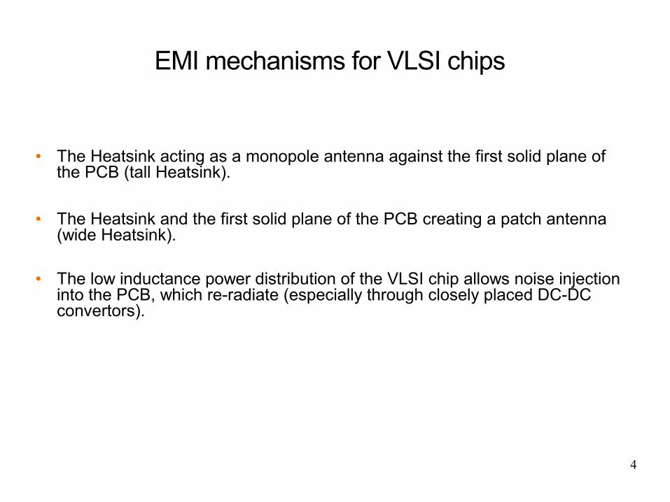
EMI mechanisms for VLSI chips
• The Heatsink acting as a monopole antenna against the first solid plane of the PCB (tall Heatsink).
• The Heatsink and the first solid plane of the PCB creating a patch antenna (wide Heatsink).
• The low inductance power distribution of the VLSI chip allows noise injection into the PCB, which re-radiate (especially through closely placed DC-DC convertors).

5
The Heatsink as a monopole and cavity resonance
(PCI_E Switch - 5GHz)

6
The Heatsink as a monopole and cavity resonance
(PCI_E Switch - 5GHz)
7
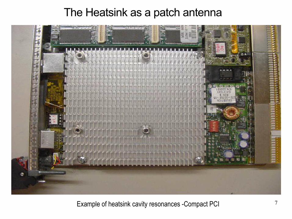
The Heatsink as a patch antenna
Example of heatsink cavity resonances -Compact PCI
8
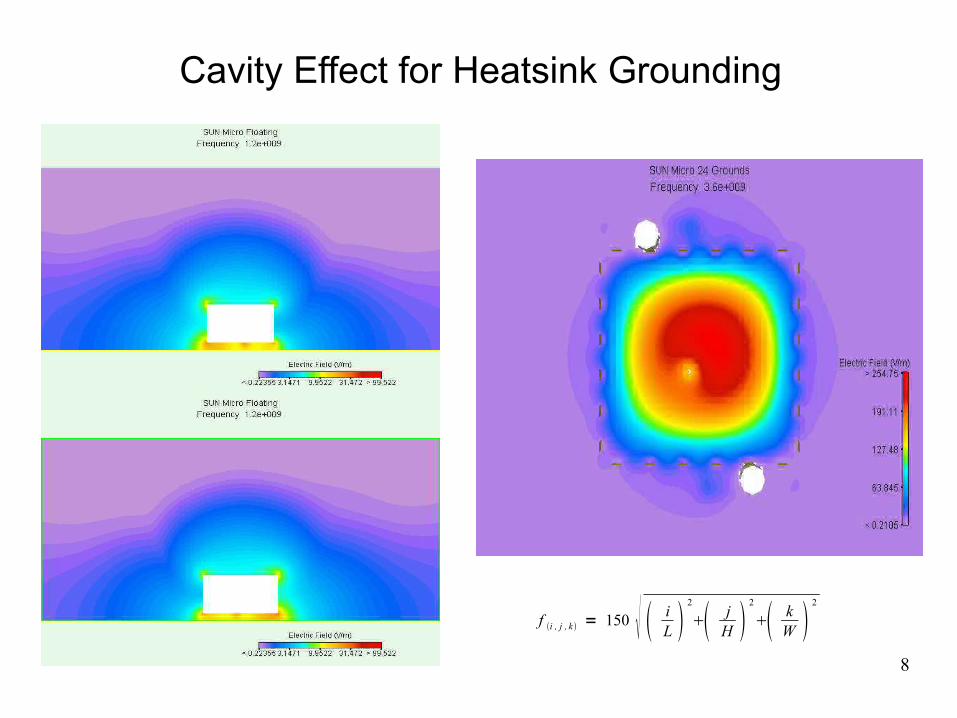
Cavity Effect for Heatsink Grounding
f i , j , k = 150 iL
2
jH
2
kW
2

9
Outline
• Introduction. EMI mechanisms for VLSI chips
• Heatsink effect for large VLSI chips
• Back-bias impact on EMI
• Integrated and separated power distribution
• Noise injection into the PCB
• Package level improvements for EMI
• Die level improvements for EMI
• Second harmonic emissions
• Power distribution issues
• Spread Spectrum Clock Generation
• Die-shrink impact on EMI
• Conclusions

10
The typical heatsink grounding
Grounding ring and EMI gasket on top layer PCB

11
Example: UltraSPARC IIIe in Sun Ultra 60
Heatsink Actually Grounded

12
Ultra Sparc T2+ CPU Provision for Grounding. Heatsink not grounded, use SSCG instead.
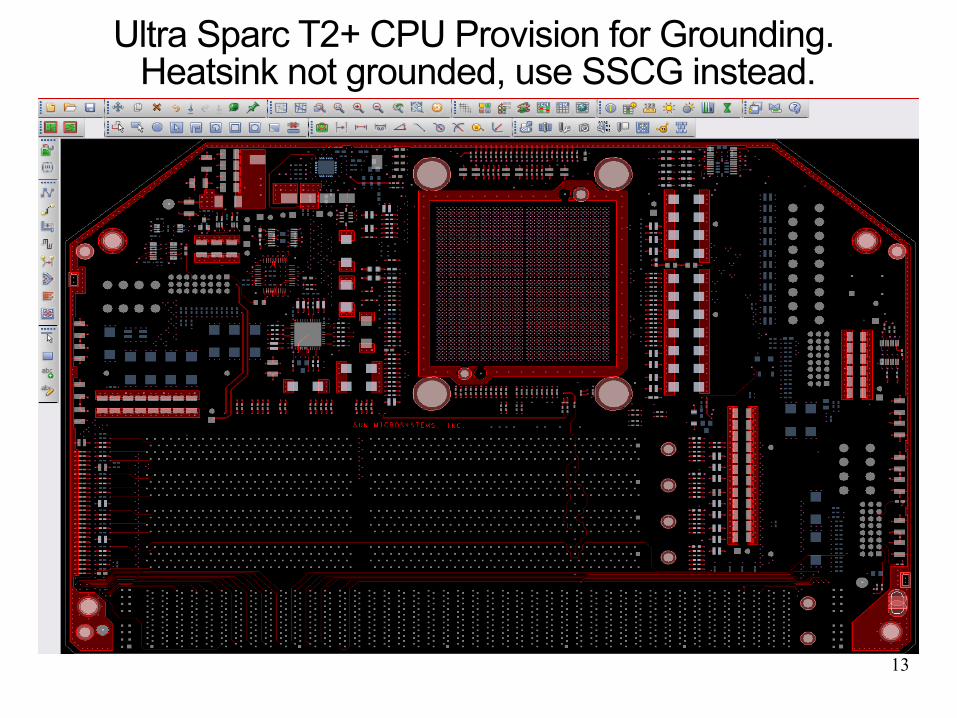
13
Ultra Sparc T2+ CPU Provision for Grounding. Heatsink not grounded, use SSCG instead.

14
Typical problems with heatsink grounding
● Components on Top need to be placed at a distance (some decoupling and terminations may be impacted)
● No pin escapes on Top
● The routing might be impacted by the multiple vias from the GND ring to GND plane
● Not effective above aprox. 1.5GHz (any grounding will be too inductiveto really matter)
● No direct DC grounding if the chip can use Back Bias or Forward Bias.
15
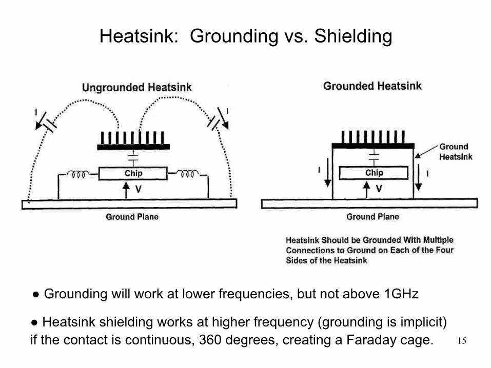
Heatsink: Grounding vs. Shielding
● Grounding will work at lower frequencies, but not above 1GHz
● Heatsink shielding works at higher frequency (grounding is implicit)if the contact is continuous, 360 degrees, creating a Faraday cage.
16
Outline
• Introduction. EMI mechanisms for VLSI chips
• Heatsink effect for large VLSI chips
• Back-bias impact on EMI
• Integrated and separated power distribution
• Noise injection into the PCB
• Package level improvements for EMI
• Die level improvements for EMI
• Second harmonic emissions
• Power distribution issues
• Spread Spectrum Clock Generation
• Die-shrink impact on EMI
• Conclusions

17
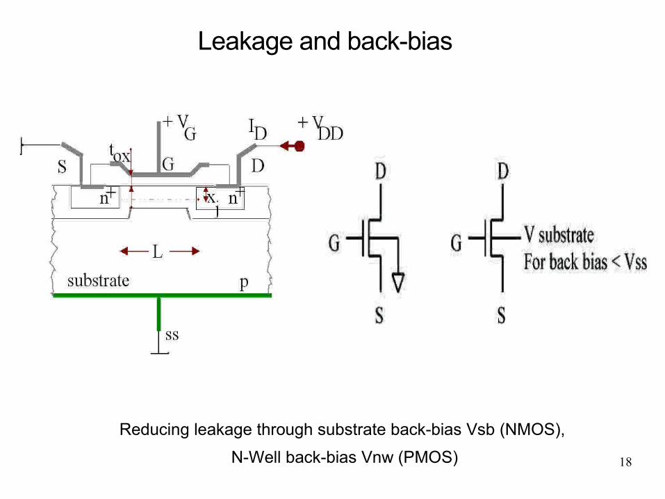
Leakage and back-bias
• Leakage is very significant problem (90nm and below it may be tens of A, especially during burn-in)
• Leakage may be reduced in multiple ways, including SOI process, strain silicon, etc.
• Back-bias allow to increase Vt and reduce Vdd
• Back-bias is one simple method to reduce the dominant leakage, and is making the heatsink grounding impossible.
• For this class of chips the package is most likely lidless and has no insulating TIM between die and heatsink.
18
Leakage and back-bias
Reducing leakage through substrate back-bias Vsb (NMOS),
N-Well back-bias Vnw (PMOS)
19
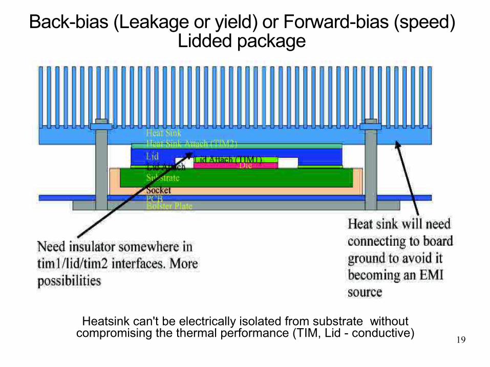
Back-bias (Leakage or yield) or Forward-bias (speed) Lidded package
Heatsink can't be electrically isolated from substrate without compromising the thermal performance (TIM, Lid - conductive)
20
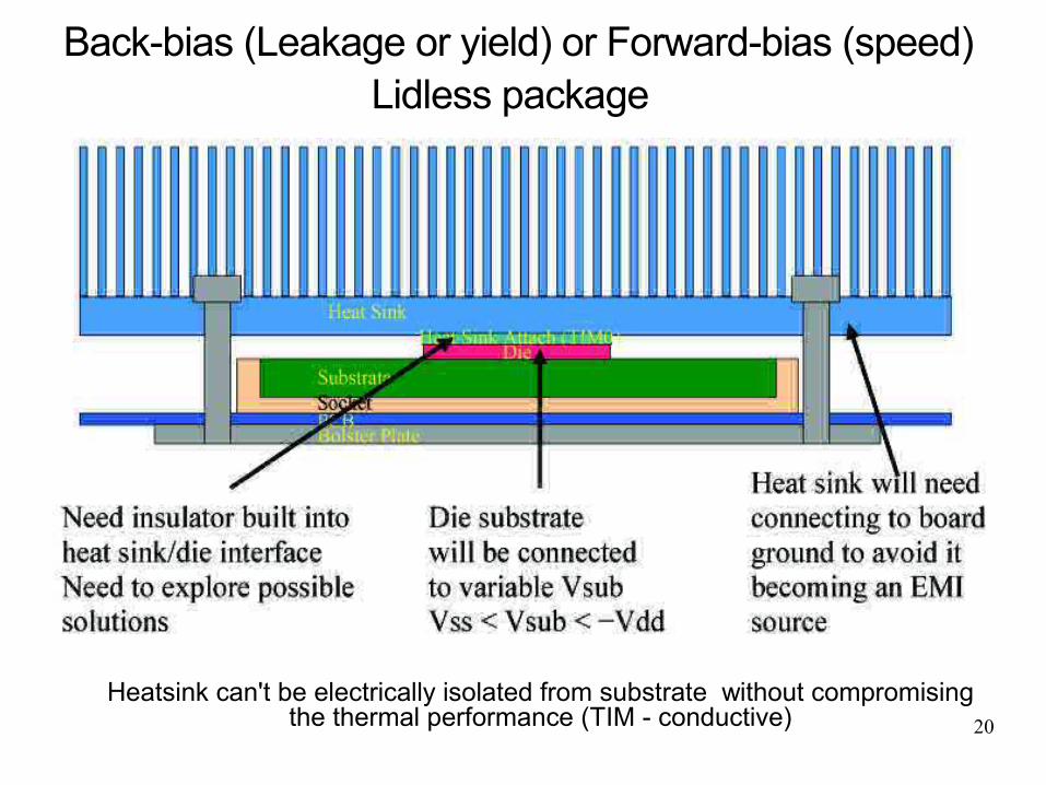
Back-bias (Leakage or yield) or Forward-bias (speed) Lidless package
Heatsink can't be electrically isolated from substrate without compromising the thermal performance (TIM - conductive)

21
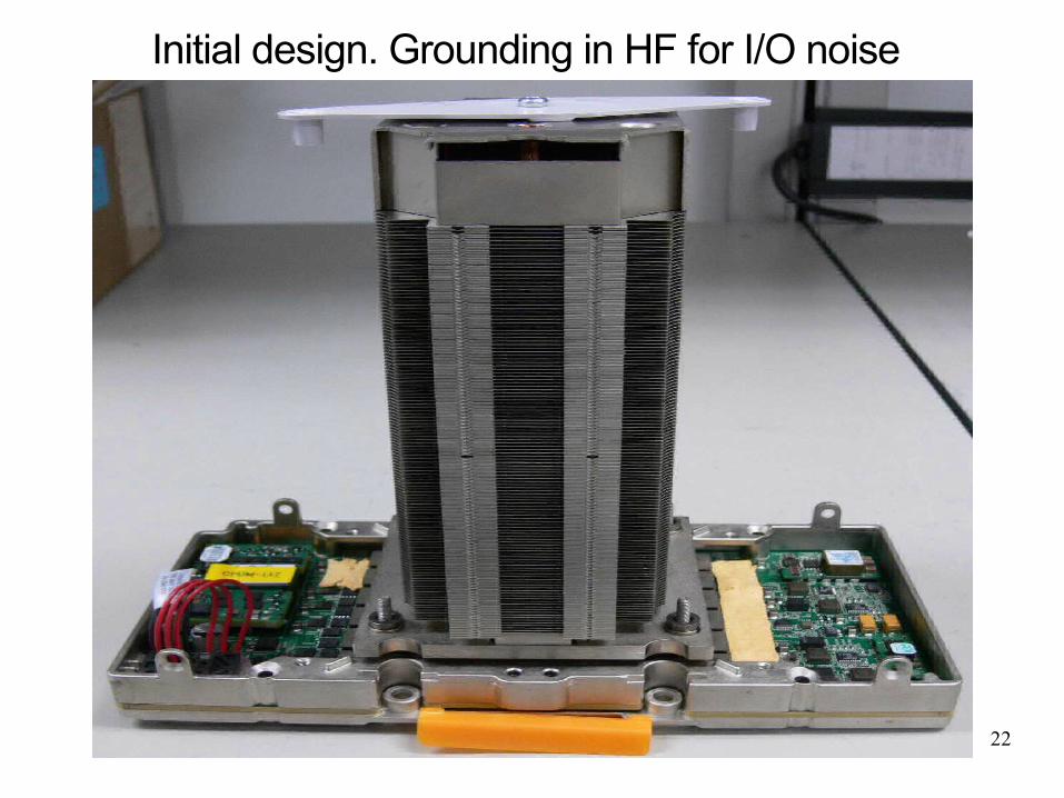
Back-bias (Leakage) . Grounding in HF for I/O noise
For ac grounding a built in cap can be added between the insulated heatsink and the CPU's chip lid
22
Initial design. Grounding in HF for I/O noise

23
Outline
• Introduction. EMI mechanisms for VLSI chips
• Heatsink effect for large VLSI chips
• Back-bias impact on EMI
• Integrated and separated power distribution
• Noise injection into the PCB
• Package level improvements for EMI
• Die level improvements for EMI
• Second harmonic emissions
• Power distribution issues
• Spread Spectrum Clock Generation
• Die-shrink impact on EMI
• Conclusions

24
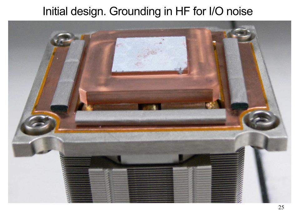
Initial design. Grounding in HF for I/O noise
25
Initial design. Grounding in HF for I/O noise

26
Alternative design. Grounding in HF for I/O noise

27
Alternative design. Grounding in HF for I/O noise
28
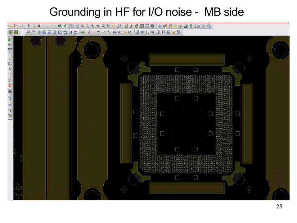
Grounding in HF for I/O noise - MB side

29
Grounding in HF for I/O noise - MB side
30
Outline
• Introduction. EMI mechanisms for VLSI chips
• Heatsink effect for large VLSI chips
• Back-bias impact on EMI
• Integrated and separated power distribution
• Noise injection into the PCB
• Package level improvements for EMI
• Die level improvements for EMI
• Second harmonic emissions
• Power distribution issues
• Spread Spectrum Clock Generation
• Die-shrink impact on EMI
• Conclusions

31
VLSI injecting noise into the PCB
μPGA (more inductive) and LGA (less inductive)
32
VLSI injecting noise into the PCB
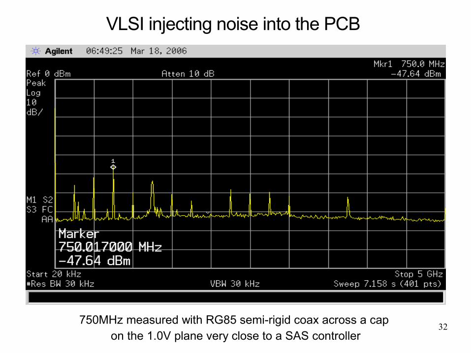
750MHz measured with RG85 semi-rigid coax across a cap on the 1.0V plane very close to a SAS controller
33
VLSI injecting noise into the PCB
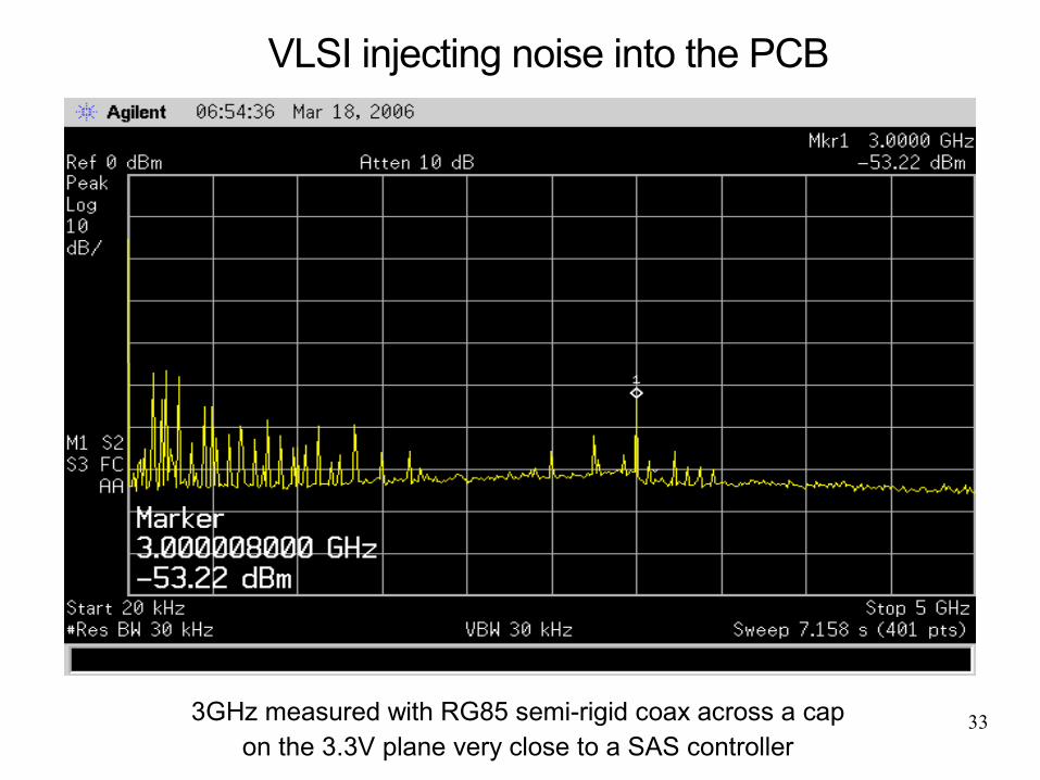
3GHz measured with RG85 semi-rigid coax across a cap on the 3.3V plane very close to a SAS controller
34
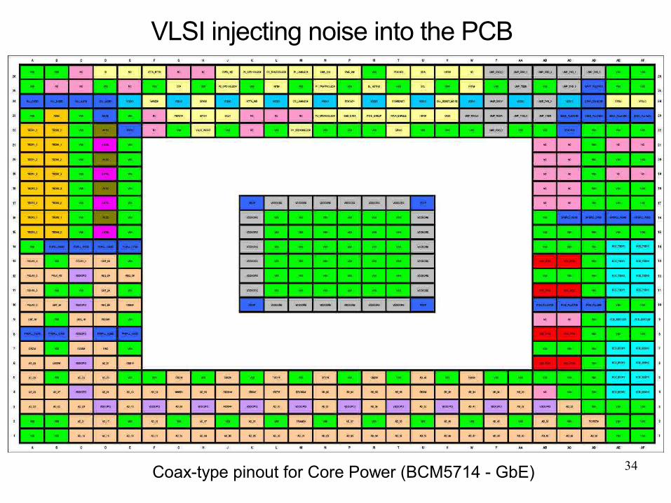
VLSI injecting noise into the PCB
Coax-type pinout for Core Power (BCM5714 - GbE)
35
Outline
• Introduction. EMI mechanisms for VLSI chips
• Heatsink effect for large VLSI chips
• Back-bias impact on EMI
• Integrated and separated power distribution
• Noise injection into the PCB
• Package level improvements for EMI
• Die level improvements for EMI
• Second harmonic emissions
• Power distribution issues
• Spread Spectrum Clock Generation
• Die-shrink impact on EMI
• Conclusions
36
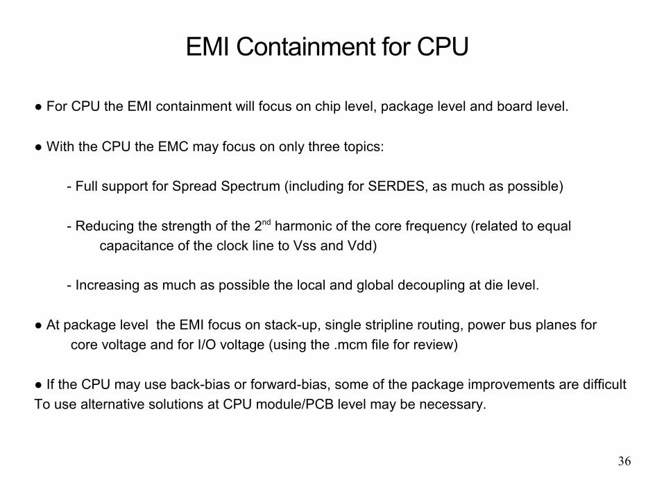
EMI Containment for CPU
● For CPU the EMI containment will focus on chip level, package level and board level.
● With the CPU the EMC may focus on only three topics:
- Full support for Spread Spectrum (including for SERDES, as much as possible)
- Reducing the strength of the 2nd harmonic of the core frequency (related to equalcapacitance of the clock line to Vss and Vdd)
- Increasing as much as possible the local and global decoupling at die level.
● At package level the EMI focus on stack-up, single stripline routing, power bus planes for core voltage and for I/O voltage (using the .mcm file for review)
● If the CPU may use back-bias or forward-bias, some of the package improvements are difficult To use alternative solutions at CPU module/PCB level may be necessary.

37
Package level improvements
• Unified GND planes for I/O and Core
• Stitching of the GND planes
• Locally grounded lid
• Dedicated power bus structures for Core & I/O
• Stripline routing for all critical signals

38
Package level improvements
Old CPU with split GND planes for I/O and Core
39
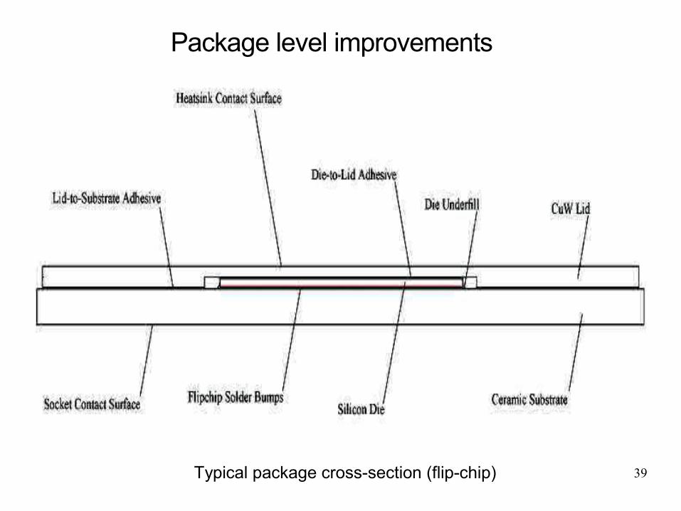
Package level improvements
Typical package cross-section (flip-chip)
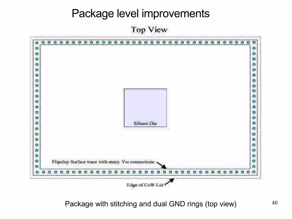
40
Package level improvements
Package with stitching and dual GND rings (top view)

41
Back Bias Issues
Lid connects to the Vss ringNo Vss ring, ring used for package
alignment, no connection to pkg GND

42
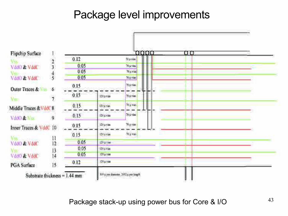
Package level improvements
Typical package stack-up using stitching & lid grounding
43
Package level improvements
Package stack-up using power bus for Core & I/O
44
Package
• Vss ring on Top + conductive adhesive
• Vss on MP2 and MP17 (18 metal layers)
• Stitching Vss on the periphery (1mm pitch)
• For Core, Vdd and Vss alternate in all layers in order to maximize the decoupling.
• No signal crossing any gaps in the V planes
• Discrete low inductance caps (8 terminals, 120pH, 30pcs.) on top of the package
• All signal pairs matched for length.
• Low inductance PDS (Pwr:GND ratio 1:1)

45
Aggregated effect on EMI (20dB)
Open chassis emissions for two fully exercised systems
One CPU system at 1.2GHz (older: 18.6dB over Class A)
Two CPU system at 1.6GHz (newer: 3.6 dB over Class B)
46
Outline
• Introduction. EMI mechanisms for VLSI chips
• Heatsink effect for large VLSI chips
• Back-bias impact on EMI
• Integrated and separated power distribution
• Noise injection into the PCB
• Package level improvements for EMI
• Die level improvements for EMI
• Second harmonic emissions
• Power distribution issues
• Spread Spectrum Clock Generation
• Die-shrink impact on EMI
• Conclusions
47
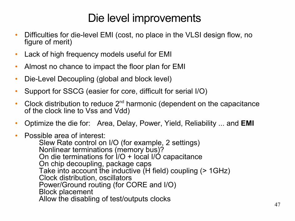
Die level improvements • Difficulties for die-level EMI (cost, no place in the VLSI design flow, no
figure of merit)
• Lack of high frequency models useful for EMI
• Almost no chance to impact the floor plan for EMI
• Die-Level Decoupling (global and block level)
• Support for SSCG (easier for core, difficult for serial I/O)
• Clock distribution to reduce 2nd harmonic (dependent on the capacitance of the clock line to Vss and Vdd)
• Optimize the die for: Area, Delay, Power, Yield, Reliability ... and EMI • Possible area of interest:
Slew Rate control on I/O (for example, 2 settings)Nonlinear terminations (memory bus)?On die terminations for I/O + local I/O capacitanceOn chip decoupling, package capsTake into account the inductive (H field) coupling (> 1GHz)Clock distribution, oscillatorsPower/Ground routing (for CORE and I/O)Block placementAllow the disabling of test/outputs clocks
48
Outline
• Introduction. EMI mechanisms for VLSI chips
• Heatsink effect for large VLSI chips
• Back-bias impact on EMI
• Integrated and separated power distribution
• Noise injection into the PCB
• Package level improvements for EMI
• Die level improvements for EMI
• Second harmonic emissions
• Power distribution issues
• Spread Spectrum Clock Generation
• Die-shrink impact on EMI
• Conclusions

49
Second Harmonic Emissions
• Currents draw on both edges of the clock
• Clock duty cycle different of 50% (minor factor -10%)
• Crowbar current in clock drivers (small factor)
• Clock driver output has nearly equal capacitance to both Vss and Vdd
(dominant factor)

50
Clock
L16-L2 clock drivers have built-in decaps (6W@2GHz)
L1CLK headers (~37,000) and flops (~162,000) do not havebuilt-in decaps (60W@2GHz)
51
Outline
• Introduction. EMI mechanisms for VLSI chips
• Heatsink effect for large VLSI chips
• Back-bias impact on EMI
• Integrated and separated power distribution
• Noise injection into the PCB
• Package level improvements for EMI
• Die level improvements for EMI
• Second harmonic emissions
• Power distribution issues
• Spread Spectrum Clock Generation
• Die-shrink impact on EMI
• Conclusions

52
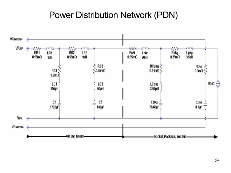
Power Distribution Network (PDN)
53
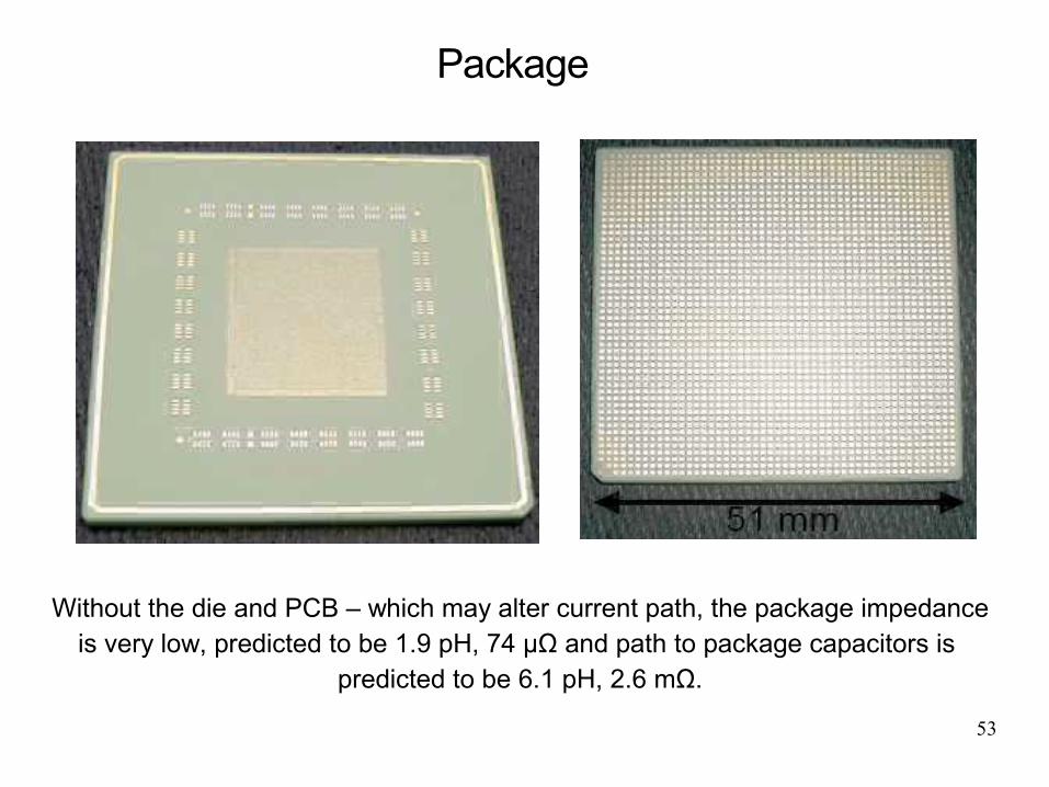
Package
Without the die and PCB – which may alter current path, the package impedanceis very low, predicted to be 1.9 pH, 74 μΩ and path to package capacitors is
predicted to be 6.1 pH, 2.6 mΩ.
54
Power Distribution Network (PDN)

55
Power Distribution Network (PDN)

56
Power Distribution Network (PDN)
Single node analysis: with and without 200 x 1nF caps on the board
57
Outline
• Introduction. EMI mechanisms for VLSI chips
• Heatsink effect for large VLSI chips
• Back-bias impact on EMI
• Integrated and separated power distribution
• Noise injection into the PCB
• Package level improvements for EMI
• Die level improvements for EMI
• Second harmonic emissions
• Power distribution issues
• Spread Spectrum Clock Generation
• Die-shrink impact on EMI
• Conclusions
58
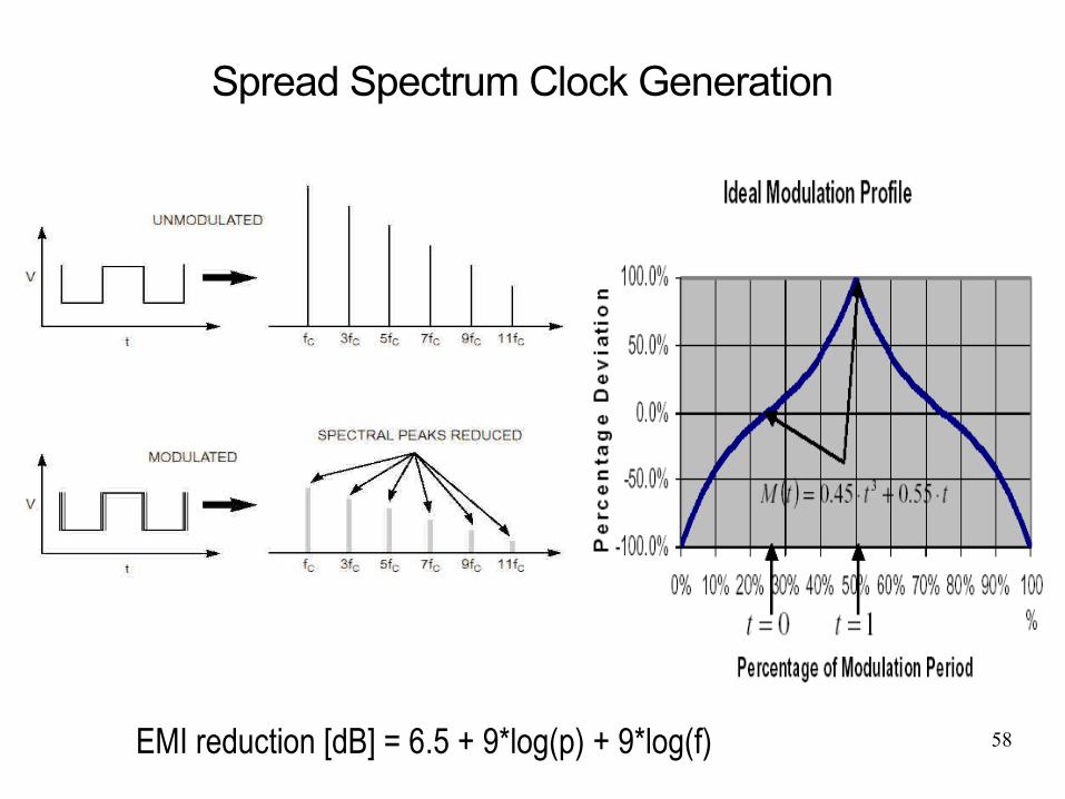
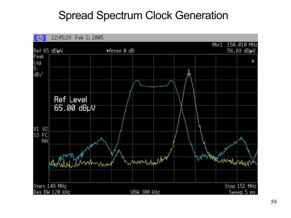
Spread Spectrum Clock Generation
EMI reduction [dB] = 6.5 + 9*log(p) + 9*log(f)
59
Spread Spectrum Clock Generation
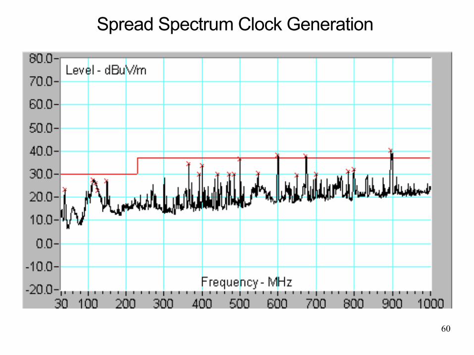
60
Spread Spectrum Clock Generation
61
Spread Spectrum Clock Generation
• Reference Clock for Clock for Core clock PLL, FBDIMM2, Coherence Links
• Spread Spectrum Clock (SSC) with up to 0.5% down spread in frequency shall be supported. The frequency of the clock and therefore bit rate can be modulated from 0% to -0.5% of the nominal data rate/frequency, at a modulation rate in the range between 30 kHz and 33 kHz. The modulation profile of SSC shall be able to provide optimal or close to optimal EMI reduction. Typical profiles include triangular or Hershey kiss profile.

62
Asynchronous Design
• Asynchronous design efforts (Sun, IBM, Intel, Philips, University of Manchester - UK).
• Pentium 4 (Intel) use elements of asynchronous design.
• Ultra Sparc IIIe use a little asynch design in the memory controller.
63
Outline
• Introduction. EMI mechanisms for VLSI chips
• Heatsink effect for large VLSI chips
• Back-bias impact on EMI
• Integrated and separated power distribution
• Noise injection into the PCB
• Package level improvements for EMI
• Die level improvements for EMI
• Second harmonic emissions
• Power distribution issues
• Spread Spectrum Clock Generation
• Die-shrink impact on EMI
• Conclusions
64
The effect of die-shrink on EMI
• The main type of die-shrink for “speed bump” is the lateral shrink (constant voltage for compatibility).
• The increase of the current, the decrease of the switching time, and the reduction of the load capacitance are expected to impact EMI.
• Multiple tests with memories and CPUs from different die-shrinks have shown variations below the level of the PVT variations (6dB).
• Different speeds do not necessarily mean die-shrink, they may be just speed bin selections.

65
Die-shrink parameters
Parameter Const. Voltage Lateral Shrink Const. E Field Generalized
Channel Length (L) 1/α 1/α
Channel Width (W) 1/α 1 1/α
Gate Oxide thickness 1/α 1 1/α
1 1 1/α
E Field in Oxide α 1 1 k
1/α 1/α
α 1/α
1/α
1/αL 1/αL
1/αW1/αL
Supply Voltage ( VDD ) k/αL
Load Capacitance ( CL ) 1/αL 1/αW
Current ( ID , Iavg ) αL k2 /αW
Gate Delay ( tpHL , tpLH ) 1/α2 1/αL2 1/αL
66
Outline
• Introduction. EMI mechanisms for VLSI chips
• Heatsink effect for large VLSI chips
• Back-bias impact on EMI
• Integrated and separated power distribution
• Noise injection into the PCB
• Package level improvements for EMI
• Die level improvements for EMI
• Second harmonic emissions
• Power distribution issues
• Spread Spectrum Clock Generation
• Die-shrink impact on EMI
• Conclusions

67
Conclusions• For core frequency over 1GHz and P>100W, very good class B performance
can be obtained with simple package improvements (stitching, internal lid grounding, dedicated power bus cores, unified ground, stripline routing).
• Die-level EMI improvements are very difficult to implement, but focusing on SSCG support, on-die decoupling and 2nd harmonic reduction might be enough, and can be achieved easier.
• PVT (Process/Voltage/Temperature) variations can impact the EMI signature significantly, up to 6dB.
• Constant voltage die-shrink at the same technology node seems to have less than expected impact.
• Functional SI & Power integrity concerns dominate the design and reduce the EMI to an acceptable level.
• General use of differential signaling has a positive impact on SSN – even out the current draw.
• The use of high-speed serial links (PCI-E, SATA, SAS) randomize the data and further reduce the EMI.
• Back-bias and lidless chips may be an EMI challenge in the near future, especially for I/O driven emissions.
VLSI Packaging Features for EMI Containment
Sergiu Radu
Sun Microsystems, Inc.EMC Design Engineering
15 Network Circle, Menlo Park, CA [email protected]
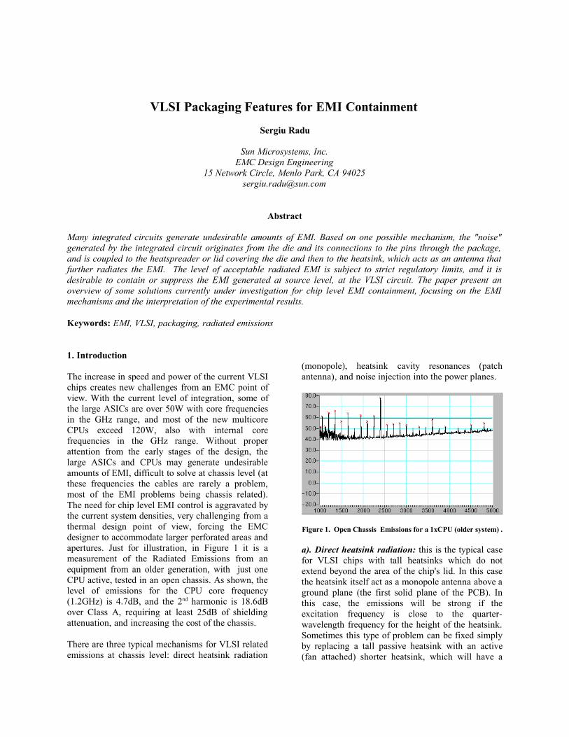
Abstract
Many integrated circuits generate undesirable amounts of EMI. Based on one possible mechanism, the "noise" generated by the integrated circuit originates from the die and its connections to the pins through the package, and is coupled to the heatspreader or lid covering the die and then to the heatsink, which acts as an antenna that further radiates the EMI. The level of acceptable radiated EMI is subject to strict regulatory limits, and it is desirable to contain or suppress the EMI generated at source level, at the VLSI circuit. The paper present an overview of some solutions currently under investigation for chip level EMI containment, focusing on the EMI mechanisms and the interpretation of the experimental results.
Keywords: EMI, VLSI, packaging, radiated emissions
1. Introduction
The increase in speed and power of the current VLSI chips creates new challenges from an EMC point of view. With the current level of integration, some of the large ASICs are over 50W with core frequencies in the GHz range, and most of the new multicore CPUs exceed 120W, also with internal core frequencies in the GHz range. Without proper attention from the early stages of the design, the large ASICs and CPUs may generate undesirable amounts of EMI, difficult to solve at chassis level (at these frequencies the cables are rarely a problem, most of the EMI problems being chassis related). The need for chip level EMI control is aggravated by the current system densities, very challenging from a thermal design point of view, forcing the EMC designer to accommodate larger perforated areas and apertures. Just for illustration, in Figure 1 it is a measurement of the Radiated Emissions from an equipment from an older generation, with just one CPU active, tested in an open chassis. As shown, the level of emissions for the CPU core frequency (1.2GHz) is 4.7dB, and the 2nd harmonic is 18.6dB over Class A, requiring at least 25dB of shielding attenuation, and increasing the cost of the chassis.
There are three typical mechanisms for VLSI related emissions at chassis level: direct heatsink radiation
(monopole), heatsink cavity resonances (patch antenna), and noise injection into the power planes.
Figure 1. Open Chassis Emissions for a 1xCPU (older system) .
a). Direct heatsink radiation: this is the typical case for VLSI chips with tall heatsinks which do not extend beyond the area of the chip's lid. In this case the heatsink itself act as a monopole antenna above a ground plane (the first solid plane of the PCB). In this case, the emissions will be strong if the excitation frequency is close to the quarter-wavelength frequency for the height of the heatsink. Sometimes this type of problem can be fixed simply by replacing a tall passive heatsink with an active (fan attached) shorter heatsink, which will have a
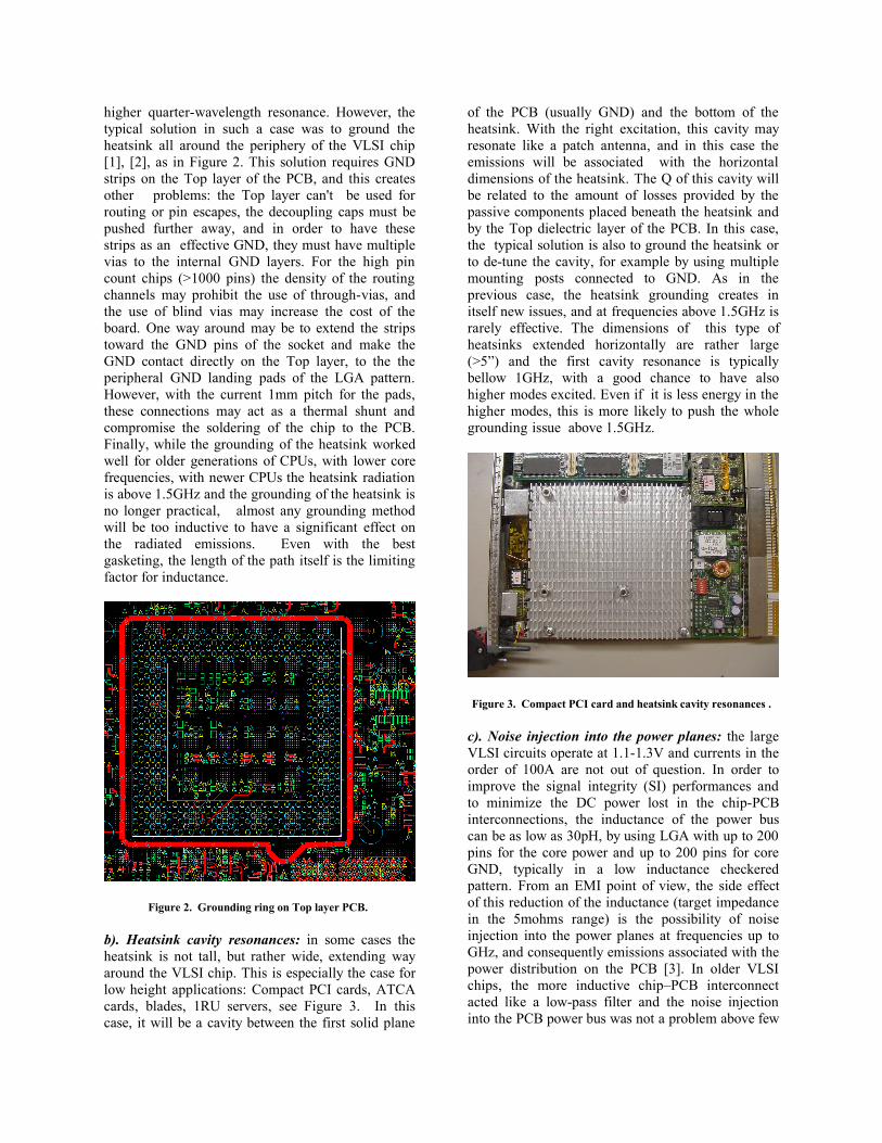
higher quarter-wavelength resonance. However, the typical solution in such a case was to ground the heatsink all around the periphery of the VLSI chip [1], [2], as in Figure 2. This solution requires GND strips on the Top layer of the PCB, and this creates other problems: the Top layer can't be used for routing or pin escapes, the decoupling caps must be pushed further away, and in order to have these strips as an effective GND, they must have multiple vias to the internal GND layers. For the high pin count chips (>1000 pins) the density of the routing channels may prohibit the use of through-vias, and the use of blind vias may increase the cost of the board. One way around may be to extend the strips toward the GND pins of the socket and make the GND contact directly on the Top layer, to the the peripheral GND landing pads of the LGA pattern. However, with the current 1mm pitch for the pads, these connections may act as a thermal shunt and compromise the soldering of the chip to the PCB. Finally, while the grounding of the heatsink worked well for older generations of CPUs, with lower core frequencies, with newer CPUs the heatsink radiation is above 1.5GHz and the grounding of the heatsink is no longer practical, almost any grounding method will be too inductive to have a significant effect on the radiated emissions. Even with the best gasketing, the length of the path itself is the limiting factor for inductance.
Figure 2. Grounding ring on Top layer PCB.
b). Heatsink cavity resonances: in some cases the heatsink is not tall, but rather wide, extending way around the VLSI chip. This is especially the case for low height applications: Compact PCI cards, ATCA cards, blades, 1RU servers, see Figure 3. In this case, it will be a cavity between the first solid plane
of the PCB (usually GND) and the bottom of the heatsink. With the right excitation, this cavity may resonate like a patch antenna, and in this case the emissions will be associated with the horizontal dimensions of the heatsink. The Q of this cavity will be related to the amount of losses provided by the passive components placed beneath the heatsink and by the Top dielectric layer of the PCB. In this case, the typical solution is also to ground the heatsink or to de-tune the cavity, for example by using multiple mounting posts connected to GND. As in the previous case, the heatsink grounding creates in itself new issues, and at frequencies above 1.5GHz is rarely effective. The dimensions of this type of heatsinks extended horizontally are rather large (>5”) and the first cavity resonance is typically bellow 1GHz, with a good chance to have also higher modes excited. Even if it is less energy in the higher modes, this is more likely to push the whole grounding issue above 1.5GHz.
Figure 3. Compact PCI card and heatsink cavity resonances .
c). Noise injection into the power planes: the large VLSI circuits operate at 1.1-1.3V and currents in the order of 100A are not out of question. In order to improve the signal integrity (SI) performances and to minimize the DC power lost in the chip-PCB interconnections, the inductance of the power bus can be as low as 30pH, by using LGA with up to 200 pins for the core power and up to 200 pins for core GND, typically in a low inductance checkered pattern. From an EMI point of view, the side effect of this reduction of the inductance (target impedance in the 5mohms range) is the possibility of noise injection into the power planes at frequencies up to GHz, and consequently emissions associated with the power distribution on the PCB [3]. In older VLSI chips, the more inductive chip–PCB interconnect acted like a low-pass filter and the noise injection into the PCB power bus was not a problem above few
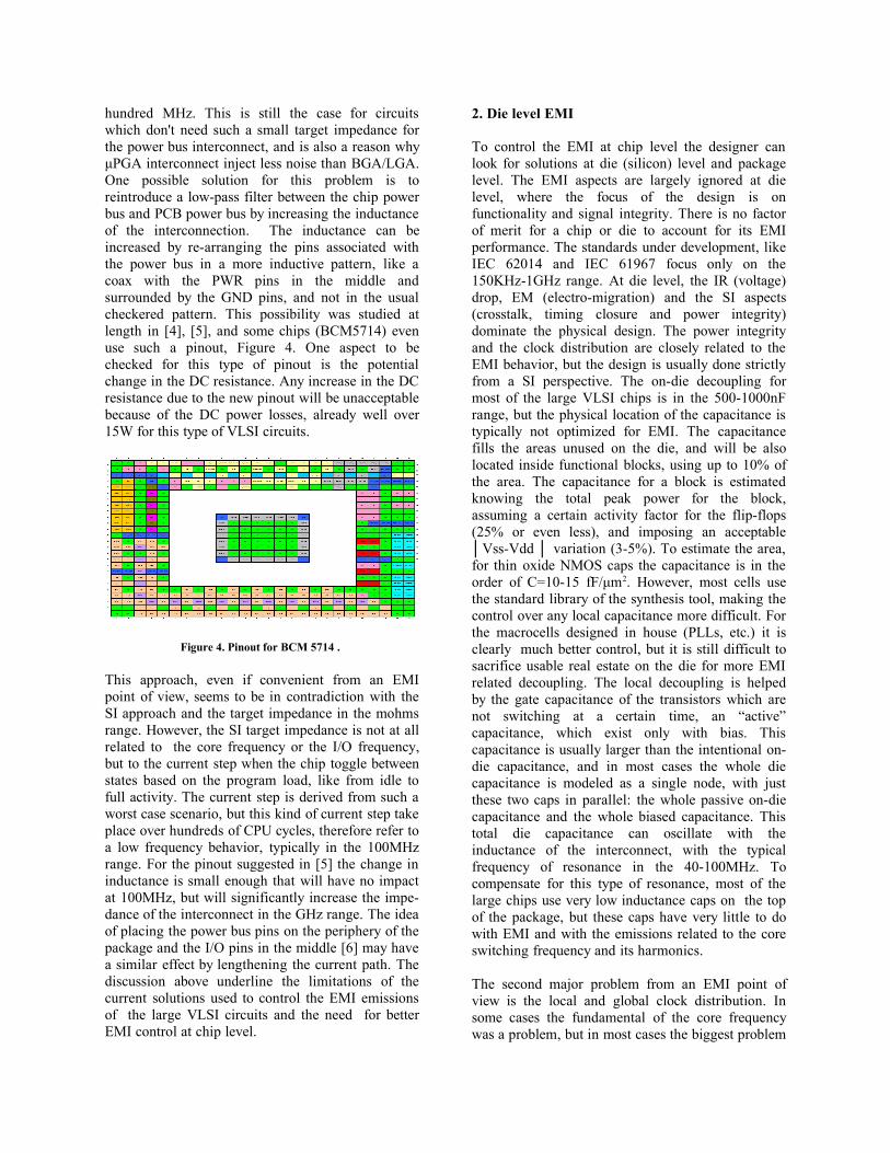
hundred MHz. This is still the case for circuits which don't need such a small target impedance for the power bus interconnect, and is also a reason why μPGA interconnect inject less noise than BGA/LGA. One possible solution for this problem is to reintroduce a low-pass filter between the chip power bus and PCB power bus by increasing the inductance of the interconnection. The inductance can be increased by re-arranging the pins associated with the power bus in a more inductive pattern, like a coax with the PWR pins in the middle and surrounded by the GND pins, and not in the usual checkered pattern. This possibility was studied at length in [4], [5], and some chips (BCM5714) even use such a pinout, Figure 4. One aspect to be checked for this type of pinout is the potential change in the DC resistance. Any increase in the DC resistance due to the new pinout will be unacceptable because of the DC power losses, already well over 15W for this type of VLSI circuits.
Figure 4. Pinout for BCM 5714 .
This approach, even if convenient from an EMI point of view, seems to be in contradiction with the SI approach and the target impedance in the mohms range. However, the SI target impedance is not at all related to the core frequency or the I/O frequency, but to the current step when the chip toggle between states based on the program load, like from idle to full activity. The current step is derived from such a worst case scenario, but this kind of current step take place over hundreds of CPU cycles, therefore refer to a low frequency behavior, typically in the 100MHz range. For the pinout suggested in [5] the change in inductance is small enough that will have no impact at 100MHz, but will significantly increase the impe-dance of the interconnect in the GHz range. The idea of placing the power bus pins on the periphery of the package and the I/O pins in the middle [6] may have a similar effect by lengthening the current path. The discussion above underline the limitations of the current solutions used to control the EMI emissions of the large VLSI circuits and the need for better EMI control at chip level.
2. Die level EMI
To control the EMI at chip level the designer can look for solutions at die (silicon) level and package level. The EMI aspects are largely ignored at die level, where the focus of the design is on functionality and signal integrity. There is no factor of merit for a chip or die to account for its EMI performance. The standards under development, like IEC 62014 and IEC 61967 focus only on the 150KHz-1GHz range. At die level, the IR (voltage) drop, EM (electro-migration) and the SI aspects (crosstalk, timing closure and power integrity) dominate the physical design. The power integrity and the clock distribution are closely related to the EMI behavior, but the design is usually done strictly from a SI perspective. The on-die decoupling for most of the large VLSI chips is in the 500-1000nF range, but the physical location of the capacitance is typically not optimized for EMI. The capacitance fills the areas unused on the die, and will be also located inside functional blocks, using up to 10% of the area. The capacitance for a block is estimated knowing the total peak power for the block, assuming a certain activity factor for the flip-flops (25% or even less), and imposing an acceptable │Vss-Vdd │ variation (3-5%). To estimate the area, for thin oxide NMOS caps the capacitance is in the order of C=10-15 fF/μm2. However, most cells use the standard library of the synthesis tool, making the control over any local capacitance more difficult. For the macrocells designed in house (PLLs, etc.) it is clearly much better control, but it is still difficult to sacrifice usable real estate on the die for more EMI related decoupling. The local decoupling is helped by the gate capacitance of the transistors which are not switching at a certain time, an “active” capacitance, which exist only with bias. This capacitance is usually larger than the intentional on-die capacitance, and in most cases the whole die capacitance is modeled as a single node, with just these two caps in parallel: the whole passive on-die capacitance and the whole biased capacitance. This total die capacitance can oscillate with the inductance of the interconnect, with the typical frequency of resonance in the 40-100MHz. To compensate for this type of resonance, most of the large chips use very low inductance caps on the top of the package, but these caps have very little to do with EMI and with the emissions related to the core switching frequency and its harmonics.
The second major problem from an EMI point of view is the local and global clock distribution. In some cases the fundamental of the core frequency was a problem, but in most cases the biggest problem
was the 2nd harmonic of the core frequency. The reason is related to the equal capacitance between the clock line and Vdd line and Vss (GND) line. Most traces on die are modeled as RC lines, however the extraction of L and RLC models for the clock line are increasingly used for timing and noise estimation in large VLSI chips.
One of the main problems for more on-die EMI, beyond the lack of accurate prediction, is the lack of EMI related rules integrated in the synthesis tools. If someone can still do a board inspection using a PCB viewer, for silicon this is practically impossible. This is one reason why most of the EMI related efforts still focus on the package.
3. Package level EMI
EMI solutions at the package level are often ignored because the main concerns at that level are the signal integrity and functionality (routing). It would be beneficial to have EMI solutions implemented at the package level because it would help reduce the need for "downstream" or add-on solutions. Some EMI improvements are suggested in [7], [8], [9]. Most of the package level solutions for EMI are in fact former board level solutions adapted for packages. The stack-up in a package follows closely the same principles as the PCB stack-up. Stitching of the GND planes on the edge of the package, a solution used for PCB, is also used for packages, less for edge radiation, and more for creating a low impedance path from the top metal layer to the internal GND planes, and also to reduce the impedance of the GND planes. In older chips, it were attempts to use different GND for I/O and different GND for Core at package level, but in the last few generations of all-digital VLSI the package uses always an unified GND. Figure 5 show one typical package stack-up:
Figure 5. Typical Stack-up for a VLSI chip .
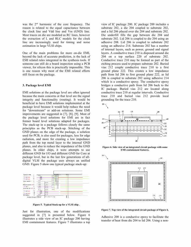
Just for illustration, one of the modifications suggested in [7] is presented below. Figure 6 illustrates a side view of an IC package 200 having EMI containment features. Figure 7 illustrates a top
view of IC package 200. IC package 200 includes a substrate 202, a die 204 coupled to substrate 202, and a lid 206 placed over die 204 and substrate 202. Die underfill fills the gap between die 204 and substrate 202. Lid 206 is coupled to die 204 using an adhesive 208. Lid 206 is coupled to substrate 202 using an adhesive 214. Substrate 202 has a number of internal layers, such as power, ground and signal layers. A conductive trace 210 is disposed around die 204 on a top surface 220 of substrate 202. Conductive trace 210 may be formed as part of the etching process used to prepare substrate 202. Buried vias 212 couple conductive trace 210 to a first ground plane 222. This creates a low impedance path from lid 206 to first ground plane 222, as lid 206 is coupled to substrate 202 using adhesive 214 which is a conductive epoxy. The conductive epoxy bridges a conductive path from lid 206 back to the IC package. Buried vias 212 are located along conductive trace 210 at regular intervals. Conductive trace 210 and buried vias 212 provide local grounding for the trace 210.
Figure 6. Side view of an integrated circuit package with some EMI containment features.
Figure 7. Top view of the integrated circuit package of Figure 6.
Adhesive 208 is a conductive epoxy to facilitate the transfer of heat from die 204 to lid 206. Using a non-
conductive epoxy may be appropriate for lower power chips because less heat is generated. If electric field effects are dominant, then using a non-conductive epoxy for adhesive 208 may also be appropriate because using a non-conductive epoxy between die 204 and lid 206 creates a higher impedance path from die 204 to lid 206. The noise source will essentially have a higher internal impedance thereby reducing the "current" flowing in the loop: from die 204 to adhesive 208 (non-conductive epoxy) to lid 206 to adhesive 214 (conductive epoxy) to trace 210 to ground plane 222 back to die 204. A conductive trace 216 is disposed around conductive trace 210 on top surface 220 of substrate 202 near the periphery of IC package 200. Conductive trace 216 may be formed as part of the etching process used to prepare substrate 202. Vias 218 couple conductive trace 216 to each of the ground planes 222, 224, 226, 228, 230. The number of ground planes between the first ground plane 222 and the last ground plane 230 may vary according to the particular IC. Trace 216 and vias 218 are part of a second EMI containment modification of IC package 200. The power planes within substrate 202 may be slightly recessed to facilitate the "stitching" together of the ground planes by vias 218. This package stitching creates a fence at the periphery of IC package 200 to help contain the noise generated by IC package 200. The package stitching may also be thought of as creating a cage, bounded by ground plane 222 and ground plane 230. Such a cage may help reduce the effects of the fringe field edge radiation, discussed below, by containing the generated noise. In Figure 6, the first (top) internal layer of substrate 202 is ground plane 222 and the last (bottom) internal layer is a power plane. Although some of the internal layers of substrate 202 may not be enclosed by the cage formed by the package stitching, the noisiest planes, particularly the power/ground pairs, are enclosed. It is even better, the top and bottom internal layers of substrate 202 are both ground planes, as the package stitching forms a cage that encloses essentially the entire internal package structure and contains more of the fringe field radiation. Vias 218 also provide low impedance paths in the same manner as vias 212. For example, the noise "current" may flow back to die 204 (instead of to a coupled heatsink) according to the following loop: from die 204 to adhesive 208 (non-conductive or conductive epoxy) to lid 206 to adhesive 214 (conductive epoxy) to trace 216 to ground plane 222 back to die 204. Additional loops exist with the other ground planes 224, 226, 228, 230. Thus, even if the fringe field radiation is not a dominant problem, the second EMI containment configuration formed in part by conductive trace 216
and vias 218 can still provide an additional level of EMI containment by providing additional low impedance paths.
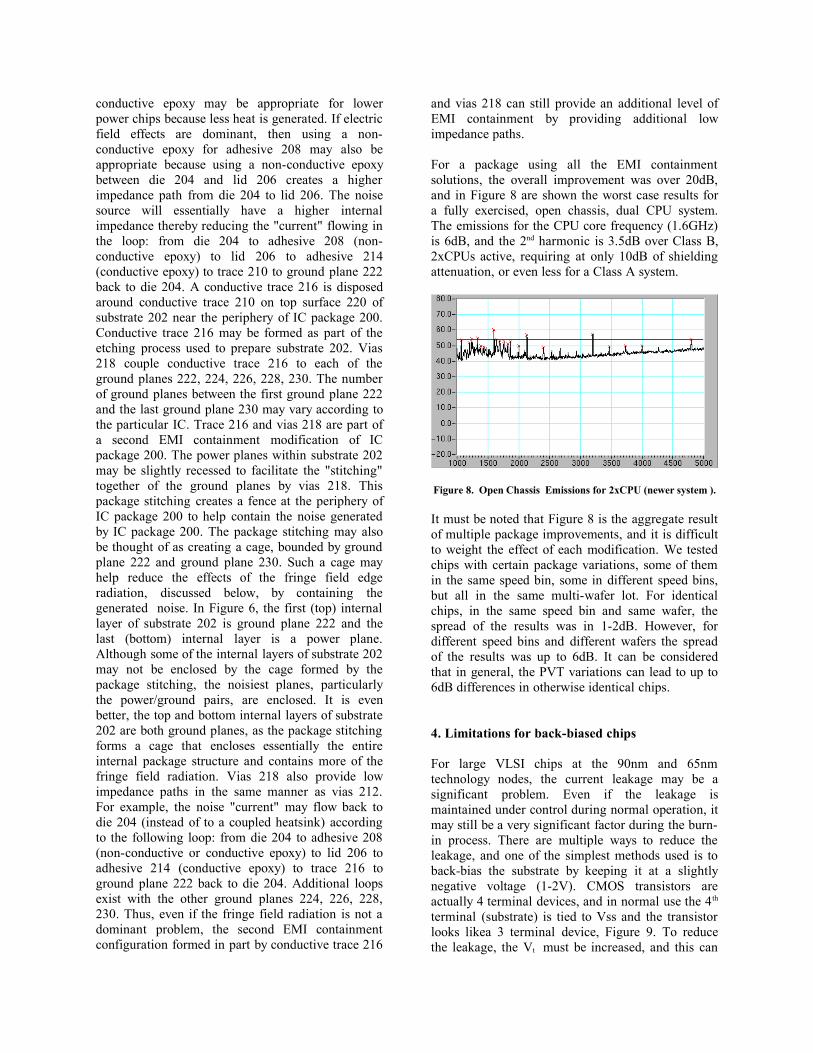
For a package using all the EMI containment solutions, the overall improvement was over 20dB, and in Figure 8 are shown the worst case results for a fully exercised, open chassis, dual CPU system. The emissions for the CPU core frequency (1.6GHz) is 6dB, and the 2nd harmonic is 3.5dB over Class B, 2xCPUs active, requiring at only 10dB of shielding attenuation, or even less for a Class A system.
Figure 8. Open Chassis Emissions for 2xCPU (newer system ).
It must be noted that Figure 8 is the aggregate result of multiple package improvements, and it is difficult to weight the effect of each modification. We tested chips with certain package variations, some of them in the same speed bin, some in different speed bins, but all in the same multi-wafer lot. For identical chips, in the same speed bin and same wafer, the spread of the results was in 1-2dB. However, for different speed bins and different wafers the spread of the results was up to 6dB. It can be considered that in general, the PVT variations can lead to up to 6dB differences in otherwise identical chips.
4. Limitations for back-biased chips
For large VLSI chips at the 90nm and 65nm technology nodes, the current leakage may be a significant problem. Even if the leakage is maintained under control during normal operation, it may still be a very significant factor during the burn-in process. There are multiple ways to reduce the leakage, and one of the simplest methods used is to back-bias the substrate by keeping it at a slightly negative voltage (1-2V). CMOS transistors are actually 4 terminal devices, and in normal use the 4th
terminal (substrate) is tied to Vss and the transistor looks likea 3 terminal device, Figure 9. To reduce the leakage, the Vt must be increased, and this can
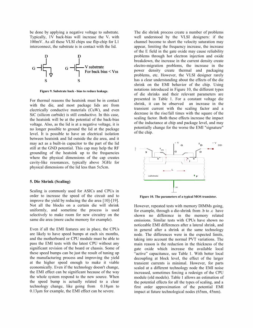
be done by applying a negative voltage to substrate. Typically, 1V back-bias will increase the Vt with 100mV. As all these VLSI chips use flip-chip for L1 interconnect, the substrate is in contact with the lid.
Figure 9. Substrate back - bias to reduce leakage.
For thermal reasons the heatsink must be in contact with the die, and most package lids are from electrically conductive materials (CuW), and even SiC (silicon carbide) is still conductive. In this case, the heatsink will be at the potential of the back-bias voltage. Also, as the lid is at a negative voltage, it is no longer possible to ground the lid at the package level. It is possible to have an electrical isolation between heatsink and lid outside the die area, and it may act as a built-in capacitor to the part of the lid still at the GND potential. This cap may help the RF grounding of the heatsink up to the frequencies where the physical dimensions of the cap creates cavity-like resonances, typically above 3GHz for physical dimensions of the lid less than 5x5cm.
5. Die Shrink (Scaling)
Scaling is commonly used for ASICs and CPUs in order to increase the speed of the circuit and to improve the yield by reducing the die area [10]-[19]. Not all the blocks on a certain die will shrink uniformly, and sometime the process is used selectively to make room for new circuitry on the same die area (more cache memory for example).
Even if all the EMI features are in place, the CPUs are likely to have speed bumps at each six months, and the motherboard or CPU module must be able to pass the EMI tests with the latest CPU without any significant revision of the board or chassis. Some of these speed bumps can be just the result of tuning up the manufacturing process and improving the yield at the higher speed enough to make it viable economically. Even if the technology doesn't change, the EMI effect can be significant because of the way the whole system respond to the new source. When the speed bump is actually related to a clear technology change, like going from 0.18μm to 0.13μm for example, the EMI effect can be severe.
The die shrink process create a number of problems well understood by the VLSI designers: if the channel become to short the velocity saturation may appear, limiting the frequency increase, the increase of the E field in the gate oxide may cause reliability problems through hot electron injection and oxide breakdown, the increase in the current density create electro-migration problems, the increase in the power density create thermal and packaging problems, etc. However, the VLSI designer rarely has a clear understanding about the effects of the die shrink on the EMI behavior of the chip. Using notations introduced in Figure 10, the different types of die shrinks and their relevant parameters are presented in Table 1. For a constant voltage die shrink, it can be observed an increase in the transient current with the scaling factor and a decrease in the rise/fall times with the square of the scaling factor. Both these effects increase the impact of the inductance at chip and package level, and may potentially change for the worse the EMI "signature" of the chip.
Figure 10. The parameters of a typical MOS transistor.
However, repeated tests with memory DIMMs going, for example, through a die-shrink from .b to .c have shown no difference in the memory related emissions. Similar tests with CPUs have shown no noticeable EMI differences after a lateral shrink, and in general after a shrink at the same technology node. The differences were in the expected limits, taking into account the normal PVT variations. The main reason is the reduction in the thickness of the gate oxide which increase the available local “active” capacitance, see Table 1. With better local decoupling at block level, the effect of the larger transient currents is minimal. However, for parts scaled at a different technology node the EMI noise increased, sometimes forcing a redesign of the CPU module (old models). Table 1 allows an estimation of the potential effects for all the types of scaling, and a first order approximation of the potential EMI impact at future technological nodes (65nm, 45nm).
substrate pp
+ V
GG DDSS
nn++ nn ++
GG
L
ss
xxjj
tt ox
+ VDD
IIDD

Table 1. Typical die shrink (scaling) methods and their parameters.
Parameter Constant Electric
Field
Constant Voltage
Lateral **
(gate shrink)
Generalized *
Long channel
Velocity Sat.
Generalized selective **
Channel Length (L) 1/α 1/α 1/αL 1/α 1/αL
Channel Width (W) 1/α 1/α 1 1/α 1/αW
Gate Oxide thickness ( tOX ) 1/α 1/α 1 1/α 1/αL
Jonction Depth ( xj ) 1/α 1/α 1 1/α 1/αL
Doping ( NA, ND ) α α2 1 kα kαL
Power Supply Voltage ( VDD ) 1/α 1 1 k/α k/αL
Wiring Width 1/α 1/α 1 1/α 1/αW
Electric Field in Oxide ( E ) 1 α 1 k k
Load Capacitance ( CL ) 1/α 1/α 1/αL 1/α 1/αW
Channel Resistance ( RD ) 1
Inversion Layer Charge Density ( Qi ) 1 α k
Depletion Layer Width ( Wd ) 1/α 1/α 1 1/α
Carrier velocity ( v ) 1 α k 1
Transconductance ( gm ) 1 α αL
Current ( ID , Iavg ) 1/α α αL k2 /α k/α k2 /αW
Current Density ( J ) α α3 αL2 k2 α kα k2 αL
Gate Delay ( tpHL , tpLH ) 1/α 1/α2 1/αL2 1/kα 1/α 1/αL
Power Dissipation/device (dynamic) 1/α2 α αL k3 /α2 k2 /α2 k2/αL αW
DC Power Dissipation 1/α2 α αL
Power Density 1 α3 αL 2 k3 k2 k2 αW/αL
Power Delay Product (figure of merit) 1/α3 1/α 1/αL k2 /α3 k2 /αL 2 αW
Gate Area 1/α2 1/α2 1/αL 1/α2 1/αL αW
Circuit Density α2 α2 αL α2 αL αW
* Constant E for k=1, constant V for k=α. Always 1 ≤ k ≤ α..
** αL denote a length scaling factor, αW a width scaling factor, k a voltage scaling factor
6. Conclusions
With the increased integration of functions in large VLSI chips and the increse in speed and power, the large ASICs and CPUs are the among the worst EMI sources in an equipment. For years, the containment solutions were mainly at PCB level and chassis level, and involved less design for better EMI at the chip level. On one hand, there are no EMI rules included in the tools for VLSI synthesis, and the package was also designed mainly from a SI perspective. On the other hand, the current trends in VLSI design will help the overall EMI performance. For example, the generalized use of differential signaling reduce the SSN and the magnetic effects at chip level, the use of source synchronous serial links removes the classic clock lines and inherently randomize the data, the reduction of the core voltage to 1.1V or less also reduce the energy of the harmonics (for a CPU, almost half of the power is dissipated in the core). Also, with the increase in the number of pins, just for routing from the flip-chip bumps to the package pins, the package need much more routing layers, most of them single striplines. It is not unusual for large VLSI circuits to have more than 12 metal layers in the ceramic package, with dedicated power bus pairs for the core and I/O voltages. All these trends, driven mainly by SI and functional concerns, will help also the EMI. However, with currents over 100A and transient currents of over 20A, the EMC design aspects need to be inegrated in the VLSI design flow. The paper is an overview of some of the chip level EMI problems and some possible solutions which were used with very good results.
References
[1] S. RADU, Y. JI, J. NUEBEL, J. L. DREWNIAK, T. P. VAN DOREN, T. H. HUBING, "Diagnosing and Modeling EMI in a Computer System with Sub-Module Testing,” in Proceedings of the 1997 IEEE International Symposium on Electromagnetic Compatibility, pp.165-170, Austin, Texas, U. S. A., August 18-22, 1997.[2] S. RADU, T. STEWART, Apparatus for Containing Electromagnetic Interference. Patent Number 6,683,796 (01/27/2004), U. S. A. [3] S. RADU, D. HOCKANSON, "An Investigation of PCB Radiated Emissions From Simultaneous Switching Noise," in Proceedings of the 1999 IEEE International Symposium on Electromagnetic Compatibility, pp.893-898, Seattle, Washington, U.S.A., August 2-6, 1999.
[4] D. HOCKANSON, R.SLONE, “Investigation of EMI Coupling at CPU Interconnect,” in Proceedings of the 2004 IEEE International Symposium on Electromagnetic Compatibility, pp. 424-429, Santa Clara, CA, U.S.A., 9-13 Aug. 2004.[5] D. M.HOCKANSON, R.D.SLONE, “Reducing Radiated Emissions from CPUs Core Power Interconnect Design,” in Proceedings of the 2005 IEEE International Symposium on Electromagnetic Compatibility, pp. 927-932, Chicago, IL, U.S.A., 8-12 Aug. 2005.[6] I. NOVAK, S.D. NOVOTNY, K. WEISS, Chip packaging and connection for reduced EMI. Patent Number 6,870,252 (3/22/2005), U. S. A.[7] S. RADU, J. WILL, S. BOYLE, D. HOCKANSON, Integrated Circuit Package with EMI Containment Features. Patent Number 6,573,590 (6/3/2003), U. S. A.[8] S. RADU, B. SEN, J. WILL, D. HOCKANSON, EMI grounding pins for CPU/ASIC chips. Patent Number 6,956,285 (10/18/2005), U. S. A. [9] S. RADU, S. BOYLE, EMI Heatspreader/Lid for Integrated Circuit Packages. Patent Number 6,943,436 (9/13/2005), U. S. A. [10] B. HOENEISEN, C. MEAD, "Fundamental Limitations in Microlectronics - I. MOS Technology," Solid State Electronics, pp.819-829, 1972.[11] R. DENNARD, "Design of Ion-Implanted MOSFET's with Very Small Physical Dimmensions," IEEE Journal of Solid State Circuits, SC-19, pp.256, 1974.[12] Y. EL-MANSY, "MOS Device and Technology Constraints in VLSI," IEEE Transactions on Electron Devices, ED-29, pp.567-573, 1982.[13] D. W. GREVE, Field Effect Devices and Applications, Prentice-Hall, 1998.[14] K. MARTIN, Digital Integrated Circuit Design, Oxford University Press, 2000.[15] Y. TAUR, T. NING, Fundamentals of Modern VLSI Design, Cambridge Press, 1998.[16] Y. TSIVIDIS, Operation and Modeling of the MOS Transistor, McGraw-Hill, 1999.[17] J. UYEMURA, CMOS Logic Circuit Design, Kluwer Academic Press, 1999.[18] N. WESTE, K. ESHRAGHIAN, Principles of CMOS VLSI Design. A System Perspective, Addison-Wesley Publishing Company, 1993.[19] W. NEBEL, Low Power Design in Deep Submicron Electronics, Kluwer Academic Publishers, 1997.