an10753 esd protection for usb 2.0 interfaces 2.0 pcb layer structure fig 10. usb 2.0...
TRANSCRIPT
Important notice Dear Customer, On 7 February 2017 the former NXP Standard Product business became a new company with the tradename Nexperia. Nexperia is an industry leading supplier of Discrete, Logic and PowerMOS semiconductors with its focus on the automotive, industrial, computing, consumer and wearable application markets In data sheets and application notes which still contain NXP or Philips Semiconductors references, use the references to Nexperia, as shown below. Instead of http://www.nxp.com, http://www.philips.com/ or http://www.semiconductors.philips.com/, use http://www.nexperia.com Instead of [email protected] or [email protected], use [email protected] (email) Replace the copyright notice at the bottom of each page or elsewhere in the document, depending on the version, as shown below: - © NXP N.V. (year). All rights reserved or © Koninklijke Philips Electronics N.V. (year). All rights reserved Should be replaced with: - © Nexperia B.V. (year). All rights reserved. If you have any questions related to the data sheet, please contact our nearest sales office via e-mail or telephone (details via [email protected]). Thank you for your cooperation and understanding,
Kind regards,
Team Nexperia

AN10753ESD protection for USB 2.0 interfacesRev. 3 — 5 February 2013 Application note
Document information
Info Content
Keywords ESD, USB, PESD5V0X1BL, PESD12VS1UL, PRTR5V0U2F, PRTR5V0U2K
Abstract This application note describes how to protect USB 2.0 ports with NXP general-application discretes parts, i.e. low-capacitance ElectroStatic Discharge (ESD) protection diodes PESD5V0X1BL, PRTR5V0U2F and PRTR5V0U2K.
NXP Semiconductors AN10753ESD protection for USB 2.0 interfaces
Revision history
Rev Date Description
3 20130205 Section 6 “Appendix” added.
2 20101101 Measurement results for PRTR5V0U2F and PRTR5V0U2K added. Table 2 “Device ESD failure threshold classification according to MIL-STD 883” added.
1 20090115 Initial version
AN10753 All information provided in this document is subject to legal disclaimers. © NXP B.V. 2013. All rights reserved.
Application note Rev. 3 — 5 February 2013 2 of 22
Contact informationFor more information, please visit: http://www.nxp.com
For sales office addresses, please send an email to: [email protected]
NXP Semiconductors AN10753ESD protection for USB 2.0 interfaces
1. Introduction
An Integrated Circuit (IC) connected to external ports can be damaged by ElectroStatic Discharge (ESD) from the operating environment.
The result of ever-shrinking IC process technology is the decrease of ESD robustness because of the smaller geometry of the silicon die.
Traditional methods to prevent ICs from ESD damage are the implementation of additional devices such as:
• Zener diodes
• Varistors
• Transient Voltage Suppressor (TVS) diodes
• Bipolar clamp diodes
However, at much higher data rates, the parasitic characteristics can distort or deteriorate signal integrity. This application note examines the general parameters the hardware designer should look at to increase the ESD robustness of the application, e.g. USB interfaces.
2. ElectroStatic Discharge (ESD) basics
ESD events are one of the most challenging issues in the semiconductor industry these days due to ever-shrinking IC structures of semiconductor devices.
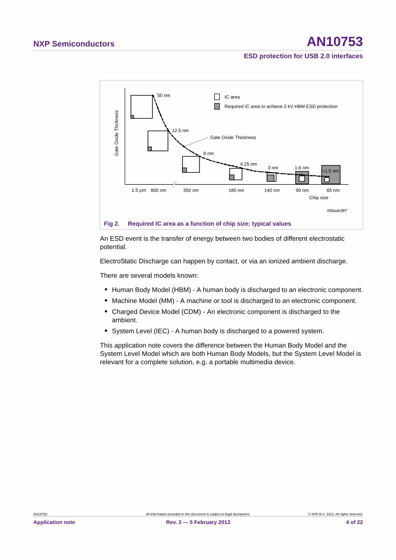
The smaller the geometry of the silicon die, the more ESD sensitive are the ICs, and the more IC area is required for the ESD protection of the device (see Figure 2).
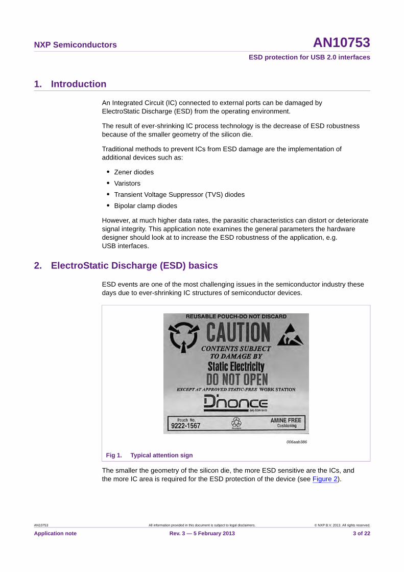
Fig 1. Typical attention sign
006aab386
AN10753 All information provided in this document is subject to legal disclaimers. © NXP B.V. 2013. All rights reserved.
Application note Rev. 3 — 5 February 2013 3 of 22
NXP Semiconductors AN10753ESD protection for USB 2.0 interfaces
An ESD event is the transfer of energy between two bodies of different electrostatic potential.
ElectroStatic Discharge can happen by contact, or via an ionized ambient discharge.
There are several models known:
• Human Body Model (HBM) - A human body is discharged to an electronic component.
• Machine Model (MM) - A machine or tool is discharged to an electronic component.
• Charged Device Model (CDM) - An electronic component is discharged to the ambient.
• System Level (IEC) - A human body is discharged to a powered system.
This application note covers the difference between the Human Body Model and the System Level Model which are both Human Body Models, but the System Level Model is relevant for a complete solution, e.g. a portable multimedia device.
Fig 2. Required IC area as a function of chip size; typical values
Gate Oxide Thickness
Required IC area to achieve 2 kV HBM ESD protection
IC area
006aab387
Chip size
Gat
e O
xide
Thi
ckne
ss
1.5 μm 800 nm 350 nm 180 nm 140 nm 90 nm 65 nm
50 nm
12.5 nm
8 nm
4.15 nm3 nm 1.6 nm
<1.5 nm
AN10753 All information provided in this document is subject to legal disclaimers. © NXP B.V. 2013. All rights reserved.
Application note Rev. 3 — 5 February 2013 4 of 22
NXP Semiconductors AN10753ESD protection for USB 2.0 interfaces
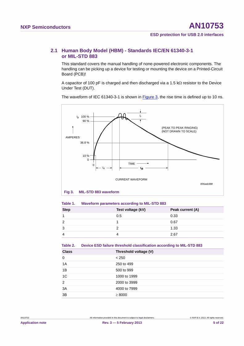
2.1 Human Body Model (HBM) - Standards IEC/EN 61340-3-1 or MIL-STD 883
This standard covers the manual handling of none-powered electronic components. The handling can be picking up a device for testing or mounting the device on a Printed-Circuit Board (PCB)!
A capacitor of 100 pF is charged and then discharged via a 1.5 k resistor to the Device Under Test (DUT).
The waveform of IEC 61340-3-1 is shown in Figure 3, the rise time is defined up to 10 ns.
Fig 3. MIL-STD 883 waveform
Table 1. Waveform parameters according to MIL-STD 883
Step Test voltage (kV) Peak current (A)
1 0.5 0.33
2 1 0.67
3 2 1.33
4 4 2.67
Table 2. Device ESD failure threshold classification according to MIL-STD 883
Class Threshold voltage (V)
0 < 250
1A 250 to 499
1B 500 to 999
1C 1000 to 1999
2 2000 to 3999
3A 4000 to 7999
3B 8000
006aab388
(PEAK TO PEAK RINGING)(NOT DRAWN TO SCALE)
CURRENT WAVEFORM
TIME
AMPERES
tdi
Ip 100 %
90 %
10 %
36.8 %
0
0tri
Ir
tdi
AN10753 All information provided in this document is subject to legal disclaimers. © NXP B.V. 2013. All rights reserved.
Application note Rev. 3 — 5 February 2013 5 of 22

NXP Semiconductors AN10753ESD protection for USB 2.0 interfaces
2.2 System Level (IEC) - Standard IEC 61000-4-2
This standard covers the manual handling of a powered electronic system, e.g. touching an interface connector.
A capacitor of 150 pF is charged and then discharged via a 330 resistor to the DUT.
The waveform of IEC 61000-4-2 is shown in Figure 4, the rise time is defined between 0.7 ns and 1 ns.
There are different levels for test proposals mentioned.
For contact or air discharge test, they differ in the voltage values (see Table 3).
Fig 4. IEC 61000-4-2 waveform
Table 3. Waveform parameters according to IEC 61000-4-2
Level Test voltage (kV) Current (A)
Contact Air Peak current After 30 ns After 60 ns
1 2 2 7.5 4 2
2 4 4 15 8 4
3 6 8 22.5 12 6
4 8 15 30 16 8
006aab389
Ipeak
100 %
90 %
t
30 ns
60 ns
10 %
tr = 0.7 ns to 1 ns
I at 30 ns
I at 60 ns
AN10753 All information provided in this document is subject to legal disclaimers. © NXP B.V. 2013. All rights reserved.
Application note Rev. 3 — 5 February 2013 6 of 22

NXP Semiconductors AN10753ESD protection for USB 2.0 interfaces
2.3 Standard comparison
Both models differentiate concerning the test voltages.
One can see that a 2 kV discharge voltage refers to different discharge currents.
Therefore, NXP recommends external ESD protection to be compliant with the IEC 61000-4-2 standard.
3. USB interface protection
The USB 2.0 standard covers several data transmission rates. It is also compliant to the former specification USB 1.1.
Following data transmission rates are covered:
• 1.5 MBit/s (low speed)
• 12.0 MBit/s (full speed)
• 480 MBit/s (hi-speed)
For the hi-speed mode, the maximum allowed capacitance according to the USB 2.0 specification is 10 pF overall.
These 10 pF are shared by a maximum of 5 pF for the transceiver itself, and the other 5 pF for the connector, PCB traces, and additional components.
Figure 5 shows the maximum allowable line capacitance at different data speeds.
To expose any issue in USB data lines, the measurement method “eye pattern”, also known as “eye diagram”, is used.
It represents a digital signal that provides minimum and maximum voltage levels and signal jitter.
Fig 5. Line capacitance as a function of line frequency; typical values
006aab390
103
f (Hz)107 108106104 105
102
10
103
Cd(pF)
1
AN10753 All information provided in this document is subject to legal disclaimers. © NXP B.V. 2013. All rights reserved.
Application note Rev. 3 — 5 February 2013 7 of 22
NXP Semiconductors AN10753ESD protection for USB 2.0 interfaces
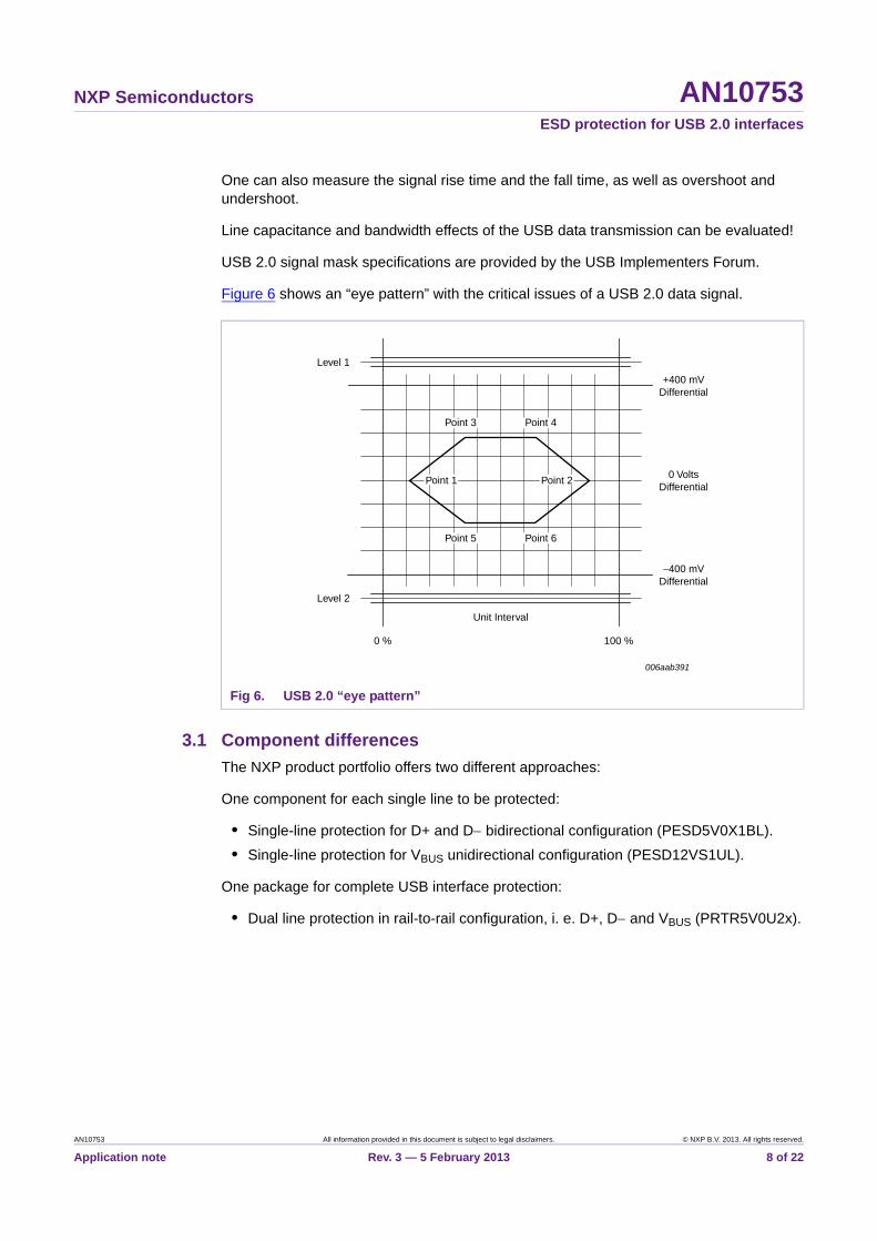
One can also measure the signal rise time and the fall time, as well as overshoot and undershoot.
Line capacitance and bandwidth effects of the USB data transmission can be evaluated!
USB 2.0 signal mask specifications are provided by the USB Implementers Forum.
Figure 6 shows an “eye pattern” with the critical issues of a USB 2.0 data signal.
3.1 Component differences
The NXP product portfolio offers two different approaches:
One component for each single line to be protected:
• Single-line protection for D+ and D bidirectional configuration (PESD5V0X1BL).
• Single-line protection for VBUS unidirectional configuration (PESD12VS1UL).
One package for complete USB interface protection:
• Dual line protection in rail-to-rail configuration, i. e. D+, D and VBUS (PRTR5V0U2x).
Fig 6. USB 2.0 “eye pattern”
006aab391
100 %
Unit Interval
Level 1
+400 mVDifferential
Level 2
0 VoltsDifferential
−400 mVDifferential
0 %
Point 3
Point 6Point 5
Point 2Point 1
Point 4
AN10753 All information provided in this document is subject to legal disclaimers. © NXP B.V. 2013. All rights reserved.
Application note Rev. 3 — 5 February 2013 8 of 22
NXP Semiconductors AN10753ESD protection for USB 2.0 interfaces
4. Measurement methods
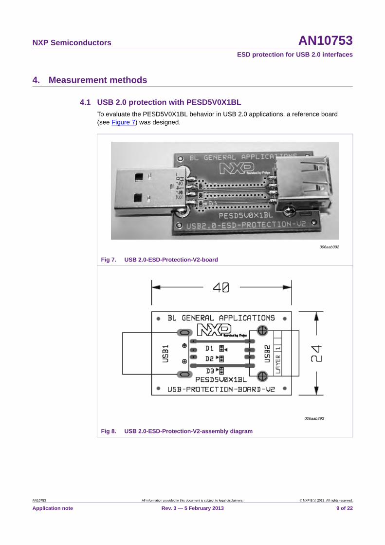
4.1 USB 2.0 protection with PESD5V0X1BL
To evaluate the PESD5V0X1BL behavior in USB 2.0 applications, a reference board (see Figure 7) was designed.
Fig 7. USB 2.0-ESD-Protection-V2-board
Fig 8. USB 2.0-ESD-Protection-V2-assembly diagram
006aab392
006aab393
AN10753 All information provided in this document is subject to legal disclaimers. © NXP B.V. 2013. All rights reserved.
Application note Rev. 3 — 5 February 2013 9 of 22

NXP Semiconductors AN10753ESD protection for USB 2.0 interfaces
An image of the PCB layer structure having two controlled impedance lines is shown in Figure 9.
Figure 10 provides the schematic of the demo board using PESD5V0X1BL for D1 and D2 each. In order to meet the USB charging requirements of even more than 5 V, there was a PESD12VS1UL chosen for D3.
Fig 9. USB 2.0 PCB layer structure
Fig 10. USB 2.0 ESD-Protection-V2-schematic
Top layer
Internal Plane 1 (GND)
Internal Plane 2 (GND)
Bottom layer
Prepreg (0.2 mm)
Core (1 mm)
Prepreg (0.2 mm)
Total height (1.529 mm)
006aab394
006aab395
USB_VBUS
USB_GND
D+
D−
CON2CON1
D1 D2 D3
PE
SD
12V
S1U
L
PE
SD
5V0X
1BL
PE
SD
5V0X
1BL
AN10753 All information provided in this document is subject to legal disclaimers. © NXP B.V. 2013. All rights reserved.
Application note Rev. 3 — 5 February 2013 10 of 22

NXP Semiconductors AN10753ESD protection for USB 2.0 interfaces
4.1.1 Reference measurements
To evaluate the influence of different ESD protection components, the measurements were done in several steps.
A board without a device was evaluated as reference.
Comparing all “eye patterns” demonstrates the degradation caused by the ESD protection devices.
The first test was done without any protection diode (see Figure 11), the result pattern is shown in Figure 13.
Fig 11. USB 2.0 “eye pattern” without DUT
Fig 12. Test setup for USB 2.0 “eye pattern” without DUT
006aab396
006aab397
AN10753 All information provided in this document is subject to legal disclaimers. © NXP B.V. 2013. All rights reserved.
Application note Rev. 3 — 5 February 2013 11 of 22

NXP Semiconductors AN10753ESD protection for USB 2.0 interfaces
4.1.2 DUT measurements
DUT measurements done on three different PCBs using two different PESD5V0X1BL diodes each are shown below.
Fig 13. USB 2.0 “eye pattern” with a 0.9 pF PESD5V0X1BL ESD protection diode; PCB1
Fig 14. USB 2.0 “eye pattern” with a 0.9 pF PESD5V0X1BL ESD protection diode; PCB2
006aab398
006aab399
AN10753 All information provided in this document is subject to legal disclaimers. © NXP B.V. 2013. All rights reserved.
Application note Rev. 3 — 5 February 2013 12 of 22
NXP Semiconductors AN10753ESD protection for USB 2.0 interfaces
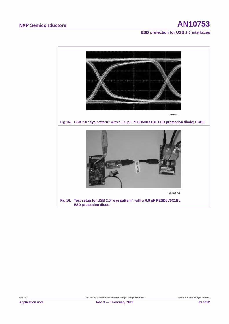
Fig 15. USB 2.0 “eye pattern” with a 0.9 pF PESD5V0X1BL ESD protection diode; PCB3
Fig 16. Test setup for USB 2.0 “eye pattern” with a 0.9 pF PESD5V0X1BL ESD protection diode
006aab400
006aab401
AN10753 All information provided in this document is subject to legal disclaimers. © NXP B.V. 2013. All rights reserved.
Application note Rev. 3 — 5 February 2013 13 of 22
NXP Semiconductors AN10753ESD protection for USB 2.0 interfaces
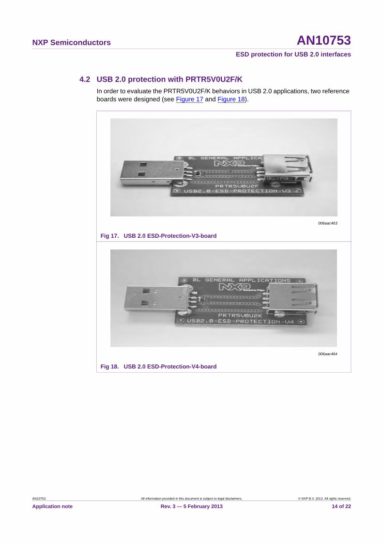
4.2 USB 2.0 protection with PRTR5V0U2F/K
In order to evaluate the PRTR5V0U2F/K behaviors in USB 2.0 applications, two reference boards were designed (see Figure 17 and Figure 18).
Fig 17. USB 2.0 ESD-Protection-V3-board
Fig 18. USB 2.0 ESD-Protection-V4-board
006aac463
006aac464
AN10753 All information provided in this document is subject to legal disclaimers. © NXP B.V. 2013. All rights reserved.
Application note Rev. 3 — 5 February 2013 14 of 22

NXP Semiconductors AN10753ESD protection for USB 2.0 interfaces
The PCB layer structure for the USB 2.0-ESD-Protection-V3/V4-assembly diagram as shown in Figure 19 is similar to the USB 2.0-ESD-Protection-V2-board (see Figure 9).
Figure 20 provides the schematic of both, V3 and V4 reference boards, with only slight differences with respect to the packages. PRTR5V0U2F is housed in an SOT886 package of dimensions 1.45 × 1 × 0.5 mm, and PRTR5V0U2K is housed in an SOT891 package of dimensions 1 × 1 × 0.5 mm.
Fig 19. USB 2.0-ESD-Protection-V3/V4-assembly diagram
Fig 20. USB 2.0-ESD-Protection-V3/V4-schematic
006aac465
006aac466
VBUS
D−
D+
GND
VBUS
D−
D+
GND
USB CONNECTOR Hi-SPEED USB TRANSCEIVER
1
2
3
6
5
4
AN10753 All information provided in this document is subject to legal disclaimers. © NXP B.V. 2013. All rights reserved.
Application note Rev. 3 — 5 February 2013 15 of 22

NXP Semiconductors AN10753ESD protection for USB 2.0 interfaces
4.2.1 Reference measurements
To evaluate the influence of different ESD protection components, the measurements were done in several steps.
A board without a device was evaluated as reference.
Comparing all “eye patterns” demonstrates the degradation caused by the ESD protection devices.
The first test was done without any protection diode (see Figure 21) using a similar test setup to Figure 12.
Fig 21. USB 2.0 “eye pattern” without DUT
006aac467
AN10753 All information provided in this document is subject to legal disclaimers. © NXP B.V. 2013. All rights reserved.
Application note Rev. 3 — 5 February 2013 16 of 22
NXP Semiconductors AN10753ESD protection for USB 2.0 interfaces
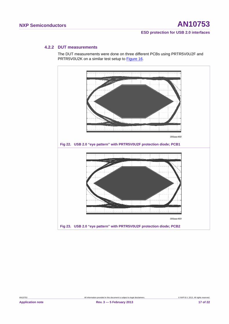
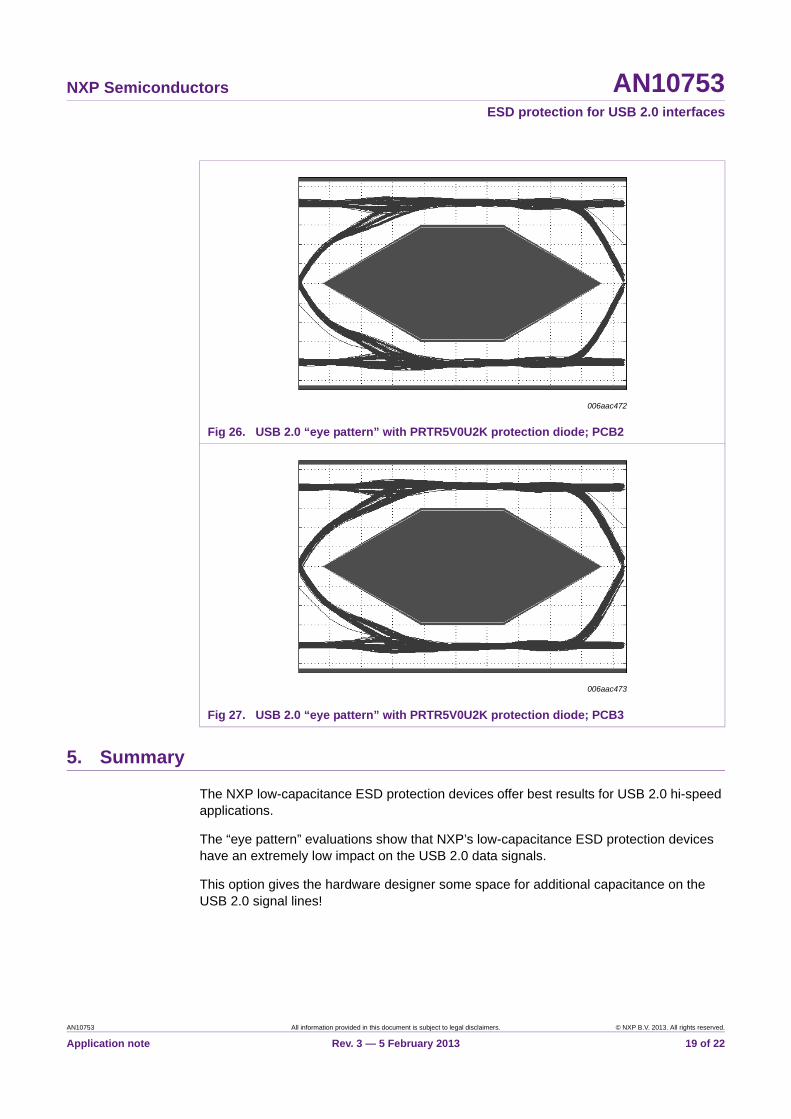
4.2.2 DUT measurements
The DUT measurements were done on three different PCBs using PRTR5V0U2F and PRTR5V0U2K on a similar test setup to Figure 16.
Fig 22. USB 2.0 “eye pattern” with PRTR5V0U2F protection diode; PCB1
Fig 23. USB 2.0 “eye pattern” with PRTR5V0U2F protection diode; PCB2
006aac468
006aac469
AN10753 All information provided in this document is subject to legal disclaimers. © NXP B.V. 2013. All rights reserved.
Application note Rev. 3 — 5 February 2013 17 of 22

NXP Semiconductors AN10753ESD protection for USB 2.0 interfaces
Fig 24. USB 2.0 “eye pattern” with PRTR5V0U2F protection diode; PCB3
Fig 25. USB 2.0 “eye pattern” with PRTR5V0U2K protection diode; PCB1
006aac470
006aac471
AN10753 All information provided in this document is subject to legal disclaimers. © NXP B.V. 2013. All rights reserved.
Application note Rev. 3 — 5 February 2013 18 of 22
NXP Semiconductors AN10753ESD protection for USB 2.0 interfaces
5. Summary
The NXP low-capacitance ESD protection devices offer best results for USB 2.0 hi-speed applications.
The “eye pattern” evaluations show that NXP’s low-capacitance ESD protection devices have an extremely low impact on the USB 2.0 data signals.
This option gives the hardware designer some space for additional capacitance on the USB 2.0 signal lines!
Fig 26. USB 2.0 “eye pattern” with PRTR5V0U2K protection diode; PCB2
Fig 27. USB 2.0 “eye pattern” with PRTR5V0U2K protection diode; PCB3
006aac472
006aac473
AN10753 All information provided in this document is subject to legal disclaimers. © NXP B.V. 2013. All rights reserved.
Application note Rev. 3 — 5 February 2013 19 of 22
NXP Semiconductors AN10753ESD protection for USB 2.0 interfaces
6. Appendix
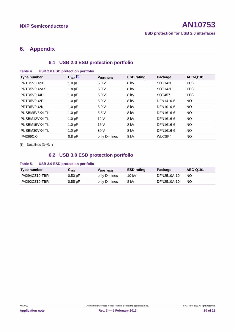
6.1 USB 2.0 ESD protection portfolio
[1] Data lines (D+/D)
6.2 USB 3.0 ESD protection portfolio
Table 4. USB 2.0 ESD protection portfolio
Type number Cline [1] VBUS(max) ESD rating Package AEC-Q101
PRTR5V0U2X 1.0 pF 5.0 V 8 kV SOT143B YES
PRTR5V0U2AX 1.8 pF 5.0 V 8 kV SOT143B YES
PRTR5V0U4D 1.0 pF 5.0 V 8 kV SOT457 YES
PRTR5V0U2F 1.0 pF 5.0 V 8 kV DFN1410-6 NO
PRTR5V0U2K 1.0 pF 5.0 V 8 kV DFN1010-6 NO
PUSBM5V5X4-TL 1.0 pF 5.5 V 8 kV DFN1616-6 NO
PUSBM12VX4-TL 1.0 pF 12 V 8 kV DFN1616-6 NO
PUSBM15VX4-TL 1.0 pF 15 V 8 kV DFN1616-6 NO
PUSBM30VX4-TL 1.0 pF 30 V 8 kV DFN1616-6 NO
IP4369CX4 0.8 pF only D lines 8 kV WLCSP4 NO
Table 5. USB 3.0 ESD protection portfolio
Type number Cline VBUS(max) ESD rating Package AEC-Q101
IP4294CZ10-TBR 0.50 pF only D lines 10 kV DFN2510A-10 NO
IP4292CZ10-TBR 0.55 pF only D lines 8 kV DFN2510A-10 NO
AN10753 All information provided in this document is subject to legal disclaimers. © NXP B.V. 2013. All rights reserved.
Application note Rev. 3 — 5 February 2013 20 of 22

NXP Semiconductors AN10753ESD protection for USB 2.0 interfaces
7. Legal information
7.1 Definitions
Draft — The document is a draft version only. The content is still under internal review and subject to formal approval, which may result in modifications or additions. NXP Semiconductors does not give any representations or warranties as to the accuracy or completeness of information included herein and shall have no liability for the consequences of use of such information.
7.2 Disclaimers
Limited warranty and liability — Information in this document is believed to be accurate and reliable. However, NXP Semiconductors does not give any representations or warranties, expressed or implied, as to the accuracy or completeness of such information and shall have no liability for the consequences of use of such information. NXP Semiconductors takes no responsibility for the content in this document if provided by an information source outside of NXP Semiconductors.
In no event shall NXP Semiconductors be liable for any indirect, incidental, punitive, special or consequential damages (including - without limitation - lost profits, lost savings, business interruption, costs related to the removal or replacement of any products or rework charges) whether or not such damages are based on tort (including negligence), warranty, breach of contract or any other legal theory.
Notwithstanding any damages that customer might incur for any reason whatsoever, NXP Semiconductors’ aggregate and cumulative liability towards customer for the products described herein shall be limited in accordance with the Terms and conditions of commercial sale of NXP Semiconductors.
Right to make changes — NXP Semiconductors reserves the right to make changes to information published in this document, including without limitation specifications and product descriptions, at any time and without notice. This document supersedes and replaces all information supplied prior to the publication hereof.
Suitability for use — NXP Semiconductors products are not designed, authorized or warranted to be suitable for use in life support, life-critical or safety-critical systems or equipment, nor in applications where failure or malfunction of an NXP Semiconductors product can reasonably be expected to result in personal injury, death or severe property or environmental damage. NXP Semiconductors and its suppliers accept no liability for inclusion and/or use of NXP Semiconductors products in such equipment or applications and therefore such inclusion and/or use is at the customer’s own risk.
Applications — Applications that are described herein for any of these products are for illustrative purposes only. NXP Semiconductors makes no representation or warranty that such applications will be suitable for the specified use without further testing or modification.
Customers are responsible for the design and operation of their applications and products using NXP Semiconductors products, and NXP Semiconductors accepts no liability for any assistance with applications or customer product design. It is customer’s sole responsibility to determine whether the NXP Semiconductors product is suitable and fit for the customer’s applications and products planned, as well as for the planned application and use of customer’s third party customer(s). Customers should provide appropriate design and operating safeguards to minimize the risks associated with their applications and products.
NXP Semiconductors does not accept any liability related to any default, damage, costs or problem which is based on any weakness or default in the customer’s applications or products, or the application or use by customer’s third party customer(s). Customer is responsible for doing all necessary testing for the customer’s applications and products using NXP Semiconductors products in order to avoid a default of the applications and the products or of the application or use by customer’s third party customer(s). NXP does not accept any liability in this respect.
Export control — This document as well as the item(s) described herein may be subject to export control regulations. Export might require a prior authorization from competent authorities.
Evaluation products — This product is provided on an “as is” and “with all faults” basis for evaluation purposes only. NXP Semiconductors, its affiliates and their suppliers expressly disclaim all warranties, whether express, implied or statutory, including but not limited to the implied warranties of non-infringement, merchantability and fitness for a particular purpose. The entire risk as to the quality, or arising out of the use or performance, of this product remains with customer.
In no event shall NXP Semiconductors, its affiliates or their suppliers be liable to customer for any special, indirect, consequential, punitive or incidental damages (including without limitation damages for loss of business, business interruption, loss of use, loss of data or information, and the like) arising out the use of or inability to use the product, whether or not based on tort (including negligence), strict liability, breach of contract, breach of warranty or any other theory, even if advised of the possibility of such damages.
Notwithstanding any damages that customer might incur for any reason whatsoever (including without limitation, all damages referenced above and all direct or general damages), the entire liability of NXP Semiconductors, its affiliates and their suppliers and customer’s exclusive remedy for all of the foregoing shall be limited to actual damages incurred by customer based on reasonable reliance up to the greater of the amount actually paid by customer for the product or five dollars (US$5.00). The foregoing limitations, exclusions and disclaimers shall apply to the maximum extent permitted by applicable law, even if any remedy fails of its essential purpose.
7.3 TrademarksNotice: All referenced brands, product names, service names and trademarks are the property of their respective owners.
AN10753 All information provided in this document is subject to legal disclaimers. © NXP B.V. 2013. All rights reserved.
Application note Rev. 3 — 5 February 2013 21 of 22

NXP Semiconductors AN10753ESD protection for USB 2.0 interfaces
8. Contents
1 Introduction . . . . . . . . . . . . . . . . . . . . . . . . . . . . 3
2 ElectroStatic Discharge (ESD) basics . . . . . . . 32.1 Human Body Model (HBM) - Standards IEC/EN
61340-3-1 or MIL-STD 883. . . . . . . . . . . . . . . . 52.2 System Level (IEC) - Standard IEC 61000-4-2. 62.3 Standard comparison . . . . . . . . . . . . . . . . . . . . 7
3 USB interface protection. . . . . . . . . . . . . . . . . . 73.1 Component differences. . . . . . . . . . . . . . . . . . . 8
4 Measurement methods . . . . . . . . . . . . . . . . . . . 94.1 USB 2.0 protection with PESD5V0X1BL . . . . . 94.1.1 Reference measurements . . . . . . . . . . . . . . . 114.1.2 DUT measurements . . . . . . . . . . . . . . . . . . . . 124.2 USB 2.0 protection with PRTR5V0U2F/K. . . . 144.2.1 Reference measurements . . . . . . . . . . . . . . . 164.2.2 DUT measurements . . . . . . . . . . . . . . . . . . . . 17
5 Summary . . . . . . . . . . . . . . . . . . . . . . . . . . . . . 19
6 Appendix . . . . . . . . . . . . . . . . . . . . . . . . . . . . . 206.1 USB 2.0 ESD protection portfolio . . . . . . . . . . 206.2 USB 3.0 ESD protection portfolio . . . . . . . . . . 20
7 Legal information. . . . . . . . . . . . . . . . . . . . . . . 217.1 Definitions. . . . . . . . . . . . . . . . . . . . . . . . . . . . 217.2 Disclaimers . . . . . . . . . . . . . . . . . . . . . . . . . . . 217.3 Trademarks. . . . . . . . . . . . . . . . . . . . . . . . . . . 21
8 Contents . . . . . . . . . . . . . . . . . . . . . . . . . . . . . . 22
© NXP B.V. 2013. All rights reserved.
For more information, please visit: http://www.nxp.comFor sales office addresses, please send an email to: [email protected]
Date of release: 5 February 2013
Document identifier: AN10753
Please be aware that important notices concerning this document and the product(s)described herein, have been included in section ‘Legal information’.