an2585 application note - rs...
TRANSCRIPT

October 2007 Rev 2 1/38
AN2585Application note
Application examples of the STM32F101xxand STM32F103xx core and system peripherals
IntroductionThe STM32F10xxx is built around the latest Cortex™-M3 core from ARM® designed for advanced microcontrollers. Its specific Thumb®-2 instruction set delivers 32-bit performance using 16-bit code density.
The STM32F10xxx has three low-power modes with a fast startup capability using the embedded 8 MHz RC oscillator. The STM32F10xxx also embeds a real-time clock running from either an internal 40 kHz RC or an external quartz oscillator.In addition, the STM32F10xxx has the VBAT function that allows it to operate from the battery for portable applications and ultralow power consumption.Security and safety are also key features of the STM32F10xxx owing to an embedded reset circuitry, a dual watchdog architecture (including an independent watchdog running from its own clock source), a backup clock in case of main oscillator failure, and anti-tamper and backup register functions.
This application note is intended to provide practical application examples of the different STM32F10xxx features listed above. The Cortex-M3 and a number of peripherals are addressed: the NVIC, SysTick, DMA, RCC, EXTI, PWR, BKP, RTC, Flash memory, IWDG and WWDG.
This document, its associated firmware, and other such application notes are written to accompany the STM32F10xxx firmware library. These are available for download from the STMicroelectronics website: www.st.com.
www.st.com
Contents AN2585 - Application note
2/38
Contents
1 Cortex™-M3 core . . . . . . . . . . . . . . . . . . . . . . . . . . . . . . . . . . . . . . . . . . . . 6
1.1 How to use Cortex™-M3 bit-band access . . . . . . . . . . . . . . . . . . . . . . . . . 6
1.1.1 Overview . . . . . . . . . . . . . . . . . . . . . . . . . . . . . . . . . . . . . . . . . . . . . . . . . 6
1.1.2 Firmware description . . . . . . . . . . . . . . . . . . . . . . . . . . . . . . . . . . . . . . . . 7
1.2 How to modify the Cortex-M3 Privileged Thread mode and the stack used 7
1.2.1 Overview . . . . . . . . . . . . . . . . . . . . . . . . . . . . . . . . . . . . . . . . . . . . . . . . . 7
1.2.2 Firmware description . . . . . . . . . . . . . . . . . . . . . . . . . . . . . . . . . . . . . . . . 7
2 NVIC application examples . . . . . . . . . . . . . . . . . . . . . . . . . . . . . . . . . . . 8
2.1 STM32F10xxx NVIC: preemption and subpriority handling . . . . . . . . . . . . 8
2.1.1 Hardware description . . . . . . . . . . . . . . . . . . . . . . . . . . . . . . . . . . . . . . . . 8
2.1.2 Firmware description . . . . . . . . . . . . . . . . . . . . . . . . . . . . . . . . . . . . . . . . 9
2.2 STM32F10xxx NVIC: IRQ channel interrupts . . . . . . . . . . . . . . . . . . . . . 10
2.2.1 Hardware description . . . . . . . . . . . . . . . . . . . . . . . . . . . . . . . . . . . . . . . 10
2.2.2 Firmware description . . . . . . . . . . . . . . . . . . . . . . . . . . . . . . . . . . . . . . . 10
2.3 STM32F10xxx NVIC: system handlers . . . . . . . . . . . . . . . . . . . . . . . . . . 11
2.3.1 Hardware description . . . . . . . . . . . . . . . . . . . . . . . . . . . . . . . . . . . . . . . 11
2.3.2 Firmware description . . . . . . . . . . . . . . . . . . . . . . . . . . . . . . . . . . . . . . . 11
2.4 STM32F10xxx NVIC: WFE and WFI modes . . . . . . . . . . . . . . . . . . . . . . 12
2.4.1 Hardware description . . . . . . . . . . . . . . . . . . . . . . . . . . . . . . . . . . . . . . . 12
2.4.2 Firmware description . . . . . . . . . . . . . . . . . . . . . . . . . . . . . . . . . . . . . . . 13
2.5 STM32F10xxx NVIC: DMA in WFI mode . . . . . . . . . . . . . . . . . . . . . . . . . 15
2.5.1 Hardware description . . . . . . . . . . . . . . . . . . . . . . . . . . . . . . . . . . . . . . . 15
2.5.2 Firmware description . . . . . . . . . . . . . . . . . . . . . . . . . . . . . . . . . . . . . . . 15
2.6 STM32F10xxx NVIC: vector table implementation with offset . . . . . . . . . 16
2.6.1 Hardware description . . . . . . . . . . . . . . . . . . . . . . . . . . . . . . . . . . . . . . . 16
2.6.2 Firmware description . . . . . . . . . . . . . . . . . . . . . . . . . . . . . . . . . . . . . . . 16
3 How to use the STM32F10xxx SysTick . . . . . . . . . . . . . . . . . . . . . . . . . 17
3.1 Hardware description . . . . . . . . . . . . . . . . . . . . . . . . . . . . . . . . . . . . . . . . 17
3.2 Firmware description . . . . . . . . . . . . . . . . . . . . . . . . . . . . . . . . . . . . . . . . 17
4 DMA application examples . . . . . . . . . . . . . . . . . . . . . . . . . . . . . . . . . . . 18

AN2585 - Application note Contents
3/38
4.1 STM32F10xxx Flash to RAM data transfer using DMA . . . . . . . . . . . . . . 18
4.1.1 Hardware description . . . . . . . . . . . . . . . . . . . . . . . . . . . . . . . . . . . . . . . 18
4.1.2 Firmware description . . . . . . . . . . . . . . . . . . . . . . . . . . . . . . . . . . . . . . . 18
4.1.3 Conclusion . . . . . . . . . . . . . . . . . . . . . . . . . . . . . . . . . . . . . . . . . . . . . . . 18
4.2 STM32F10xxx I2C-to-I2C communication using DMA . . . . . . . . . . . . . . . 19
4.2.1 Hardware description . . . . . . . . . . . . . . . . . . . . . . . . . . . . . . . . . . . . . . . 19
4.2.2 Firmware description . . . . . . . . . . . . . . . . . . . . . . . . . . . . . . . . . . . . . . . 19
4.2.3 Conclusion . . . . . . . . . . . . . . . . . . . . . . . . . . . . . . . . . . . . . . . . . . . . . . . 19
4.3 STM32F10xxx full-duplex, SPI-to-SPI communication using DMA . . . . . 20
4.3.1 Hardware description . . . . . . . . . . . . . . . . . . . . . . . . . . . . . . . . . . . . . . . 20
4.3.2 Firmware description . . . . . . . . . . . . . . . . . . . . . . . . . . . . . . . . . . . . . . . 20
4.3.3 Conclusion . . . . . . . . . . . . . . . . . . . . . . . . . . . . . . . . . . . . . . . . . . . . . . . 21
4.4 STM32F10xxx peripheral-to-peripheral data transfer using DMA . . . . . . 21
4.4.1 Hardware description . . . . . . . . . . . . . . . . . . . . . . . . . . . . . . . . . . . . . . . 21
4.4.2 Firmware description . . . . . . . . . . . . . . . . . . . . . . . . . . . . . . . . . . . . . . . 21
4.4.3 Conclusion . . . . . . . . . . . . . . . . . . . . . . . . . . . . . . . . . . . . . . . . . . . . . . . 21
5 RCC application examples . . . . . . . . . . . . . . . . . . . . . . . . . . . . . . . . . . . 22
5.1 How to use the STM32F10xxx RCC . . . . . . . . . . . . . . . . . . . . . . . . . . . . 22
5.1.1 Hardware description . . . . . . . . . . . . . . . . . . . . . . . . . . . . . . . . . . . . . . . 22
5.1.2 Firmware description . . . . . . . . . . . . . . . . . . . . . . . . . . . . . . . . . . . . . . . 22
6 How to use the STM32F10xxx EXTI controller . . . . . . . . . . . . . . . . . . . 23
6.1 Hardware description . . . . . . . . . . . . . . . . . . . . . . . . . . . . . . . . . . . . . . . . 23
6.2 Firmware description . . . . . . . . . . . . . . . . . . . . . . . . . . . . . . . . . . . . . . . . 23
6.3 Conclusion . . . . . . . . . . . . . . . . . . . . . . . . . . . . . . . . . . . . . . . . . . . . . . . . 23
7 PWR application examples . . . . . . . . . . . . . . . . . . . . . . . . . . . . . . . . . . . 24
7.1 STM32F10xxx Stop mode . . . . . . . . . . . . . . . . . . . . . . . . . . . . . . . . . . . . 24
7.1.1 Hardware description . . . . . . . . . . . . . . . . . . . . . . . . . . . . . . . . . . . . . . . 24
7.1.2 Firmware description . . . . . . . . . . . . . . . . . . . . . . . . . . . . . . . . . . . . . . . 24
7.2 STM32F10xxx Standby mode . . . . . . . . . . . . . . . . . . . . . . . . . . . . . . . . . 25
7.2.1 Hardware description . . . . . . . . . . . . . . . . . . . . . . . . . . . . . . . . . . . . . . . 25
7.2.2 Firmware description . . . . . . . . . . . . . . . . . . . . . . . . . . . . . . . . . . . . . . . 26
8 BKP application examples . . . . . . . . . . . . . . . . . . . . . . . . . . . . . . . . . . . 27
Contents AN2585 - Application note
4/38
8.1 How to write/read data to/from Backup data registers . . . . . . . . . . . . . . . 27
8.1.1 Hardware description . . . . . . . . . . . . . . . . . . . . . . . . . . . . . . . . . . . . . . . 27
8.1.2 Firmware description . . . . . . . . . . . . . . . . . . . . . . . . . . . . . . . . . . . . . . . 27
8.2 How to store user data into the Backup data registers . . . . . . . . . . . . . . . 28
8.2.1 Hardware description . . . . . . . . . . . . . . . . . . . . . . . . . . . . . . . . . . . . . . . 28
8.2.2 Firmware description . . . . . . . . . . . . . . . . . . . . . . . . . . . . . . . . . . . . . . . 28
9 RTC application examples . . . . . . . . . . . . . . . . . . . . . . . . . . . . . . . . . . . 30
9.1 STM32F10xxx RTC and backup (BKP) domain . . . . . . . . . . . . . . . . . . . . 30
9.1.1 Hardware description . . . . . . . . . . . . . . . . . . . . . . . . . . . . . . . . . . . . . . . 30
9.1.2 Firmware description . . . . . . . . . . . . . . . . . . . . . . . . . . . . . . . . . . . . . . . 31
10 Flash memory application examples . . . . . . . . . . . . . . . . . . . . . . . . . . . 32
10.1 How to program the STM32F10xxx Flash memory . . . . . . . . . . . . . . . . . 32
10.1.1 Firmware description . . . . . . . . . . . . . . . . . . . . . . . . . . . . . . . . . . . . . . . 32
10.2 How to enable and disable the STM32F10xxx Flash memorywrite protection . . . . . . . . . . . . . . . . . . . . . . . . . . . . . . . . . . . . . . . . . . . . . 32
10.2.1 Firmware description . . . . . . . . . . . . . . . . . . . . . . . . . . . . . . . . . . . . . . . 32
10.2.2 Enable Write protection . . . . . . . . . . . . . . . . . . . . . . . . . . . . . . . . . . . . . 33
10.2.3 Disable Write protection . . . . . . . . . . . . . . . . . . . . . . . . . . . . . . . . . . . . . 33
11 How to use the STM32F10xxx IWDG . . . . . . . . . . . . . . . . . . . . . . . . . . . 34
11.1 Hardware description . . . . . . . . . . . . . . . . . . . . . . . . . . . . . . . . . . . . . . . . 34
11.2 Firmware description . . . . . . . . . . . . . . . . . . . . . . . . . . . . . . . . . . . . . . . . 34
12 How to use the STM32F10xxx WWDG . . . . . . . . . . . . . . . . . . . . . . . . . . 35
12.1 Hardware description . . . . . . . . . . . . . . . . . . . . . . . . . . . . . . . . . . . . . . . . 35
12.2 Firmware description . . . . . . . . . . . . . . . . . . . . . . . . . . . . . . . . . . . . . . . . 35
13 Conclusion . . . . . . . . . . . . . . . . . . . . . . . . . . . . . . . . . . . . . . . . . . . . . . . . 36
14 Revision history . . . . . . . . . . . . . . . . . . . . . . . . . . . . . . . . . . . . . . . . . . . 37

AN2585 - Application note List of figures
5/38
List of figures
Figure 1. STM32F10xxx NVIC hardware connection - example 1 . . . . . . . . . . . . . . . . . . . . . . . . . . . . 8Figure 2. STM32F10xxx NVIC hardware connection - example 2 . . . . . . . . . . . . . . . . . . . . . . . . . . . 10Figure 3. STM32F10xxx NVIC hardware connection - example 3 . . . . . . . . . . . . . . . . . . . . . . . . . . . 11Figure 4. STM32F10xxx NVIC hardware connection - example 4 . . . . . . . . . . . . . . . . . . . . . . . . . . . 12Figure 5. STM32F10xxx NVIC hardware connection - example 5 . . . . . . . . . . . . . . . . . . . . . . . . . . . 15Figure 6. STM32F10xxx NVIC hardware connection - example 6 . . . . . . . . . . . . . . . . . . . . . . . . . . . 16Figure 7. STM32F10xxx example LED connection . . . . . . . . . . . . . . . . . . . . . . . . . . . . . . . . . . . . . . 17Figure 8. STM32F10xxx I2C-I2C communication . . . . . . . . . . . . . . . . . . . . . . . . . . . . . . . . . . . . . . . . 19Figure 9. STM32F10xxx full-duplex SPI-SPI communication . . . . . . . . . . . . . . . . . . . . . . . . . . . . . . 20Figure 10. STM32F10xxx ADC_IN14 connection . . . . . . . . . . . . . . . . . . . . . . . . . . . . . . . . . . . . . . . . 21Figure 11. STM32F10xxx RCC example hardware connection . . . . . . . . . . . . . . . . . . . . . . . . . . . . . . 22Figure 12. STM32F10xxx EXTI Line connection . . . . . . . . . . . . . . . . . . . . . . . . . . . . . . . . . . . . . . . . . 23Figure 13. STM32F10xxx Stop mode example hardware connection . . . . . . . . . . . . . . . . . . . . . . . . . 24Figure 14. STM32F10xxx Standby mode example hardware connection . . . . . . . . . . . . . . . . . . . . . . 25Figure 15. STM32F10xxx ANTI_TAMP connection . . . . . . . . . . . . . . . . . . . . . . . . . . . . . . . . . . . . . . . 27Figure 16. Example connection to store user data into the Backup data registers . . . . . . . . . . . . . . . 28Figure 17. STM32F10xxx RTC hardware configuration. . . . . . . . . . . . . . . . . . . . . . . . . . . . . . . . . . . . 30Figure 18. STM32F10xxx IWDG example hardware connection. . . . . . . . . . . . . . . . . . . . . . . . . . . . . 34Figure 19. STM32F10xxx WWDG example hardware connection. . . . . . . . . . . . . . . . . . . . . . . . . . . . 35

Cortex™-M3 core AN2585 - Application note
6/38
1 Cortex™-M3 core
Section 1 provides practical information on how to use some of the Cortex-M3™ core special features.
1.1 How to use Cortex™-M3 bit-band access
1.1.1 Overview
The Cortex-M3 memory map includes two bit-band regions. These regions map each word in an alias region of memory to a bit in a bit-band region of memory. Writing to a word in the alias region has the same effect as a read-modify-write operation on the targeted bit in the bit-band region.
In the STM32F10xxx, the peripheral registers and the SRAM are mapped in a bit-band region. This allows atomic bit-band write and read operations to be performed.
A mapping formula shows how to reference each word in the alias region to a corresponding bit in the bit-band region. The mapping formula is:
where:
bit_word_addr is the address of the word in the alias memory region that maps to the targeted bit
bit_band_base is the starting address of the alias region
byte_offset is the number of the byte in the bit-band region that contains the targeted bit
bit_number is the bit position (0-31) of the targeted bit
The following example shows how to map bit 2 of the byte at SRAM address 0x20000300 in the alias region:
0x2200 6008 = 0x2200 0000 + (0x300 × 32) + (2 × 4)
Writing to address 0x2200 6008 has the same effect as a read-modify-write operation on bit 2 of the byte at SRAM address 0x2000 0300.
Reading address 0x2200 6008 returns the value (0x01 or 0x00) of bit 2 of the byte at SRAM address 0x2000 0300 (0x01: bit set; 0x00: bit reset).
bit_word_addr bit_band_base byte_offset 32×( ) bit_number 4×( )+ +=
AN2585 - Application note Cortex™-M3 core
7/38
1.1.2 Firmware description
This example shows how to use Cortex-M3 bit-band access to perform atomic read-modify-write and read operations on a variable in SRAM.
The associated program declares three macros used to manipulate the variable bit: reset, set and read a specific bit using bit-band access:
#define RAM_BASE 0x20000000#define RAM_BB_BASE 0x22000000
#define Var_ResetBit_BB(VarAddr, BitNumber) \(*(vu32 *) (RAM_BB_BASE I ((VarAddr - RAM_BASE) << 5) I ((BitNumber) << 2)) = 0) #define Var_SetBit_BB(VarAddr, BitNumber) \(*(vu32 *) (RAM_BB_BASE I ((VarAddr - RAM_BASE) << 5) I ((BitNumber) << 2)) = 1)
#define Var_GetBit_BB(VarAddr, BitNumber) \(*(vu32 *) (RAM_BB_BASE I ((VarAddr - RAM_BASE) << 5) I ((BitNumber) << 2)))
As an example, a variable is declared and its value is changed using the above defined macros.
This firmware is provided as Cortex-M3 example 1 in the STM32F10xxx firmware library, available from the STMicroelectronics microcontrollers website.
1.2 How to modify the Cortex-M3 Privileged Thread mode and the stack used
1.2.1 Overview
This example shows how to modify the Cortex-M3 Thread mode’s Privileged access and stack.
1.2.2 Firmware description
Cortex-M3 Thread mode is entered on Reset, and can be entered as a result of an exception return.
The associated program is used to:
Switch the Thread mode stack from Main stack to Process stack
Switch the Thread mode from Privileged to Unprivileged
Switch the Thread mode from Unprivileged back to Privileged
To monitor the stack used and the privileged or unprivileged access level of code in Thread mode, a set of variables is available within the program. It is also possible to use the 'Cortex register' window of the debugger.
This firmware is provided as CortexM3 example 2 in the STM32F10xxx firmware library, available from the STMicroelectronics microcontrollers website.
NVIC application examples AN2585 - Application note
8/38
2 NVIC application examples
Section 2 provides practical application examples of the STM32F10xxx NVIC peripheral use.
2.1 STM32F10xxx NVIC: preemption and subpriority handlingThis section describes how to use the NVIC (nested vector interrupt controller) firmwarelibrary to demonstrate the Cortex-M3™ priority mechanism (preemption priority andsubpriority). An example is given, that uses some of the NVIC driver functionality: Enable,Set priority, Get Active IRQ status, Clear IRQ pending bit, etc.
2.1.1 Hardware description
Figure 1 shows the example hardware connection used.
Figure 1. STM32F10xxx NVIC hardware connection - example 1
STM32F10xxx
PC7
PC9
PC6
PC8
PA0
3.3 V
4.7 KΩ
100 Ω
100 nF
600 Ω
600 Ω
600 Ω
600 Ω
ai14361
PB9
3.3 V
4.7 KΩ
100 Ω
100 nF

AN2585 - Application note NVIC application examples
9/38
2.1.2 Firmware description
The provided firmware includes the NVIC driver that supports all Cortex-M3 exception andIRQ channel handlers through a set of functions. An example of use for most of thesefunctions is provided. In this example, two EXTI lines (Line0 & Line9) and the SysTickHandler are used. An interrupt is generated on each falling edge of the EXTI lines.
These interrupts are configured with the following parameters:
EXTI Line0
– PreemptionPriority = PreemptionPriorityValue
– SubPriority = 0
EXTI Line9
– PreemptionPriority = 0
– SubPriority = 1
SysTick Handler
– PreemptionPriority = !PreemptionPriorityValue
– SubPriority = 0
First, PreemptionPriorityValue is equal to 0 then EXTI Line0 has a higher preemption prioritythan the SysTick handler.
In the EXTI Line9 interrupt routine, the EXTI Line0 and SysTick preemption priorities areinverted. In the EXTI Line0 interrupt routine, the pending bit of the SysTick interrupt is set.This causes SysTick ISR to preempt the EXTI Line0 ISR only if it has a higher preemptionpriority.
The system behaves as follows:
1. The first time the EXTI Line9 interrupt occurs, the SysTick preemption becomes higher than that of EXTI Line0. So when the EXTI Line0 interrupt occurs, the SysTick ISR is executed and the PreemptionOccured variable becomes TRUE, causing the four LEDs connected to the PC6, PC7, PC8 and PC9 pins to start toggling.
2. When the next EXTI Line9 interrupt occurs, the SysTick preemption becomes lower than that of EXTI Line0. So when the EXTI Line0 interrupt occurs, the PreemptionOccured variable becomes FALSE, causing the four LEDs connected to the PC6, PC7, PC8 and PC9 pins to stop toggling.
The above described system behavior (1. and 2.)is then repeated in an infinite loop.
This firmware is provided as NVIC example 1 in the STM32F10xxx firmware library, availablefrom the STMicroelectronics microcontrollers website.

NVIC application examples AN2585 - Application note
10/38
2.2 STM32F10xxx NVIC: IRQ channel interruptsThis section describes how to use the NVIC firmware library so as to implement several IRQchannels with different priorities.
2.2.1 Hardware description
Figure 2 shows the example hardware connection used.
Figure 2. STM32F10xxx NVIC hardware connection - example 2
2.2.2 Firmware description
The provided firmware includes the NVIC driver that supports all Cortex-M3 exception andIRQ channel handlers through a set of functions. An example of use for most of thesefunctions is provided.
In the example, three IRQ channels are used: TIM2, TIM3 and TIM4 interrupt handlers.These three timers are configured to generate an interrupt on each counter update event.The IRQ channels have an ascending IRQ preemption priority, that is, TIM2 has apreemption priority of 0 and TIM4 has a preemption priority of 2.
In each interrupt routine:
TIM2 toggles the LED connected to the PC6 pin every 1 s
TIM3 toggles the LED connected to the PC7 pin every 2 s
TIM4 toggles the LED connected to the PC8 pin every 3 s
This firmware is provided as NVIC example 2 in the STM32F10xxx firmware library, availablefrom the STMicroelectronics microcontrollers website.
STM32F10xxx
PC7
PC6
PC8
600 Ω
600 Ω
600 Ω
ai14335

AN2585 - Application note NVIC application examples
11/38
2.3 STM32F10xxx NVIC: system handlersThis section describes how to use the NVIC firmware library so as to implement severalsystem handlers with different priorities.
2.3.1 Hardware description
Figure 3 shows the example hardware connection used.
Figure 3. STM32F10xxx NVIC hardware connection - example 3
2.3.2 Firmware description
The provided firmware includes the NVIC driver that supports all Cortex-M3 exception andIRQ channel handlers through a set of functions. An example of use for most of thesefunctions is provided.
In this example, fours system handlers are used: NMI, PSV, SVCall and SysTick handlers.These handlers are called in cascade mode from the SysTick handler, which is the handlermode entry point.
The handler priorities are configured as follows:
NMI has –1 preemption priority (Fixed priority)
PSV has 0 preemption priority
SVCall has 1 preemption priority
SysTick has 2 preemption priority
The SysTick timer is configured to generate an interrupt every 1 s.
In the SyStick handler routine, the LED connected to the PC6 pin toggles every 1 s and theSVC instruction is executed. This activates the SVCall handler to preempt the currentinstruction stream. In the SVCall handler routine, the LED connected to the PC7 pin togglesand the pending bit of the PSV handler is set by software. PSV, that has a higher preemptionpriority, preempts the SVCall handler and toggles the LED connected to the PC8 pin. Also, inthis handler routine, the NMI pending bit is set, which activates the NMI handler and causesthe LED connected to the PC9 pin to toggle.
This firmware is provided as NVIC example 3 in the STM32F10xxx firmware library, availablefrom the STMicroelectronics microcontrollers website.
STM32F10xxx
PC7
PC6
PC8
600 Ω
600 Ω
600 Ω
ai14336
PC9

NVIC application examples AN2585 - Application note
12/38
2.4 STM32F10xxx NVIC: WFE and WFI modesThis section describes how to use the NVIC firmware library to demonstrate the Cortex-M3low-power mode capabilities: WFE (wait for event) and WFI (wait for interrupt).
2.4.1 Hardware description
Figure 4 shows the example hardware connection used.
Figure 4. STM32F10xxx NVIC hardware connection - example 4
STM32F10xxx
PC9
PC6
PC8
PA0
3.3 V
4.7 KΩ
100 Ω
100 nF
600 Ω
600 Ω
600 Ω
ai14368
PB9
3.3 V
4.7 KΩ
100 Ω
100 nF
3.3 V
4.7 KΩ
100 Ω
100 nF
PC13
AN2585 - Application note NVIC application examples
13/38
2.4.2 Firmware description
The provided firmware includes the NVIC driver that supports all Cortex-M3 exception andIRQ channel handlers through a set of functions. An example of use for most of thesefunctions is provided.
In this example, three EXTI lines (Line0, Line9 & Line13) are used. An interrupt or event is generated on each falling edge. EXTI Line0 and Line13 are configured in Interrupt mode and EXTI Line9 is configured in Event mode. The user must select which low-power mode will be executed through five define statements in the main code. The choice is:
Wait For Interrupt (WFI) Sleep On Exit: in this case, the Cortex-M3 automatically enters the WFI mode on an exception return and the WFI instruction is not needed. The exception is executed if it has a high enough priority to run and the Cortex-M3 returns to the WFI mode. To obtain this behavior, the procedure is as follows:
– Choose the #WFISLEEPONEXIT define statement and comment other define statements
– Run the example
– The first time the EXTI Line13 event occurs, the Cortex-M3 SLEEPONEXIT bit is set. As a result the Cortex-M3 enters the WFI mode on an exception return.
– Each time the EXTI Line0 event occurs, the LED connected to PC8 pin toggles.
Any falling edge on EXTI Line0 or Line13 will execute the EXTI interrupt. On exiting the ISR, the Cortex-M3 enters the WFI mode. Whenever the EXTI Line 0 is pulled low, the Cortex-M3 exits the WFI mode, the LED connected to PC8 is toggled and the Cortex-M3 reverts to the WFI mode. This behavior is repeated in an infinite loop.
Wait For Interrupt (WFI) Sleep Now: in this mode the WFI instruction is directly executed. To obtain this behavior, the procedure is as follows:
– Choose the #WFISLEEPNOW define statement and comment other define statements
– Run the example
– In the EXTI Line13 routine, the LED connected to PC6 is toggled and the Cortex-M3 enters the WFI mode.
– To wake up the Cortex-M3, use the push-button connected to EXTI Line0, it will toggle the LED connected to PC8
This behavior is repeated in an infinite loop.

NVIC application examples AN2585 - Application note
14/38
Wait For Event (WFE) SEV ON PEND: in this mode, the WFE instruction is directly executed and the main instruction stream is boosted by the PRIMASK register (main priority = 0). To obtain this behavior, the procedure is as follows:
– Choose the #WFESEVONPEND define statement and comment other define statements
– Run the example
– In the EXTI Line13 routine, the execution priority is boosted to 0 (no other interrupt is executed once the priority has been boosted), the LED connected to PC6 is toggled and the Cortex-M3 enters the WFE mode.
– Use the push-button connected to EXTI Line0 to wake up the Cortex-M3. It will not toggle the LED connected to PC8 but will wake up the Cortex-M3 from WFE (SEV ON PEND). The EXTI Line0 interrupt passes from nonpending state to pending state, thus waking up the Cortex-M3 from WFE (the EXTI Line0 interrupt has not enough priority to run because the main execution priority is boosted to 0 using the PRIMASK register).
– The push-button connected to EXTI Line9 configured in event mode can also be used to wake up the Cortex-M3.
– If the #RTC_Alarm_WFEWakeUp define statement is enabled, the RTC alarm wakes up the Cortex-M3 after 6 seconds (if neither EXTI Line0 nor EXTI Line9 is used to wake up the Cortex-M3 during this time)
Wait For Event (WFE) SEV ON EVENT: in this mode the WFE instruction is directly executed. To obtain this behavior, the procedure is as follows:
– Choose the #WFESEVONEVENT define statement and comment the other define statements
– Run the example
– In the EXTI Line13 routine the LED connected to PC6 is toggled and the Cortex-M3 enters the WFE mode.
– Use the push-button connected to EXTI Line0 to wake up the Cortex-M3. It will toggle the LED connected to PC8.
– The push-button connected to EXTI Line9 configured in event mode can also be used to wake up the Cortex-M3.
– If the #RTC_Alarm_WFEWakeUp define statement is enabled, the RTC alarm wakes up the Cortex-M3 after 6 seconds (if neither EXTI Line0 nor EXTI Line9 is used to wake up the Cortex-M3 during this time)
This behavior is repeated in an infinite loop.
The LED connected to PC9 toggles to indicate that the Cortex-M3 is in the Run mode and not in a low-power mode.
This firmware is provided as NVIC example 4 in the STM32F10xxx firmware library, availablefrom the STMicroelectronics microcontrollers website.

AN2585 - Application note NVIC application examples
15/38
2.5 STM32F10xxx NVIC: DMA in WFI modeThis section describes how to enter the WFI mode with DMA transfer enabled and wakeupfrom this mode by the DMA End of Transfer interrupt.
2.5.1 Hardware description
Figure 5 shows four LEDs connected to the STM32F10xxx. The USART1 signals (Rx, Tx)must be connected to the DB9 connector using a RS232 transceiver. Connect a null-modemfemale/female RS232 cable between the DB9 connector (CN6 on the STM3210B-EVALboard) and the PC serial port.
Figure 5. STM32F10xxx NVIC hardware connection - example 5
2.5.2 Firmware description
The provided firmware includes the NVIC driver that supports all Cortex-M3 exception andIRQ channel handlers through a set of functions. An example of use for most of thesefunctions is provided.
In the associated firmware, the system clock is set to 72 MHz, DMA Channel5 is configuredto transfer 10 pieces of data from the USART1 data register to a predefined buffer,DST_Buffer, and to generate an interrupt at the end of the transfer.
USART1 receives data from the HyperTerminal.
The LED connected to the PC6 pin is toggled at a frequency depending on the system clock.It indicates whether the MCU is in WFI or Run mode.
A falling edge on EXTI Line 9 puts the Cortex-M3 in the WFI mode, causing the PC6 pin tostop toggling. To wake up the Cortex-M3 from the WFI mode, a sequence has to be sentfrom the HyperTerminal to USART1: 0, 1, 2, 3, 4, 5, 6, 7, 8, 9. These bytes are thentransferred by the DMA from the USART1 receive data register to the predefined buffer. Aninterrupt is then generated that causes the system to exit the WFI mode.
As a result, the LED connected to the PC6 pin starts toggling again. Likewise the LEDconnected to PC7 starts toggling if the buffer is correctly received, else it is the LEDconnected to PC8 that starts toggling.
This firmware is provided as NVIC example 5 in the STM32F10xxx firmware library, availablefrom the STMicroelectronics microcontrollers website.
STM32F10xxx
PC7
USART1_TX
PC6
PC8
PB9
3.3 V
4.7 KΩ
100 Ω
100 nF
600 Ω
600 Ω
600 Ω
ai14337
USARTtransceiver
DB9connectorUSART1_RX
to PC HyperTerminal

NVIC application examples AN2585 - Application note
16/38
2.6 STM32F10xxx NVIC: vector table implementation with offsetThis section describes how to use the NVIC firmware library to relocate the CortexM3 vectortable to a specific address that is not the default address.
2.6.1 Hardware description
Figure 6 shows the example hardware connection used.
Figure 6. STM32F10xxx NVIC hardware connection - example 6
2.6.2 Firmware description
The provided firmware describes how to use the NVIC firmware library to relocate theCortexM3 vector table to a specific address.
This can be used to build a program that will be loaded into the Flash memory by anapplication previously programmed in the sector0 of the Flash memory.
Such applications can be in-application programming (IAP, through USART) or devicefirmware upgrade (DFU, through USB). They are available for download from theSTMicroelectronics microcontrollers website.
The associated program implements a Delay function based on the SysTick end of countinterrupt. It toggles four LEDs connected to the PC6, PC7, PC8 and PC9 pins with a timingdefined by the Delay function.
When using IAP to load your program, the vector table must be relocated to address0x0800 2000.
When using DFU to load your program, the vector table must be relocated to address0x0800 3000.
This firmware is provided as NVIC example 6 in the STM32F10xxx firmware library, availablefrom the STMicroelectronics microcontrollers website.
STM32F10xxx
PC7
PC6
PC8
600 Ω
600 Ω
600 Ω
ai14336
PC9
AN2585 - Application note How to use the STM32F10xxx SysTick
17/38
3 How to use the STM32F10xxx SysTick
This section describes how to configure the Cortex-M3™ system timer (SysTick) to generate a time base. An example is given that uses most of the SysTick driver functionality: set reload value, enable and disable counter, interrupt request enable.
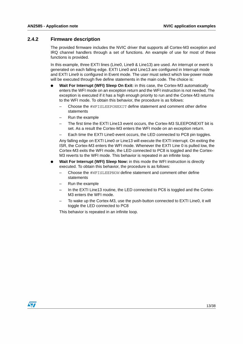
3.1 Hardware descriptionFigure 7 shows the example hardware connection used.
Figure 7. STM32F10xxx example LED connection
3.2 Firmware descriptionThe provided firmware includes the SysTick driver that supports all SysTick features through a set of functions. An example of use for most of these functions is provided.
This example shows how to configure the SysTick to generate a time base equal to 1 ms. The system clock is set to 72 MHz, the SysTick is clocked by the AHB clock (HCLK) divided by 8.
A Delay function is implemented based on the SysTick end-of-count event.
Four LEDs connected to the PC6, PC7, PC8 and PC9 pins are toggled with a timing defined by the Delay function.
This firmware is provided as SysTick example in the STM32F10xxx firmware library, available from the STMicroelectronics microcontrollers website.
STM32F10xxx
PC7
PC6
PC8
600 Ω
600 Ω
600 Ω
ai14336
PC9

DMA application examples AN2585 - Application note
18/38
4 DMA application examples
Section 4 provides practical application examples of the STM32F10xxx DMA peripheral use.
4.1 STM32F10xxx Flash to RAM data transfer using DMAThis section describes how to transfer the data buffer contents from the Flash memory to the RAM using DMA.
4.1.1 Hardware description
No hardware connection needed.
4.1.2 Firmware description
The provided firmware includes the DMA driver that supports all DMA functionalities through a set of functions.
DMA Channel6 is configured to transfer the contents of a 32-word data buffer stored in Flash memory to the reception buffer declared in RAM. Trigger is done by software. DMA Channel6 memory-to-memory transfer is enabled. Source and destination address incrementing is also enabled. The transfer is started by setting the Channel enable bit for DMA Channel6. At the end of the transfer a Transfer Complete interrupt is generated if enabled. In the routine, the remaining data to be transferred is read, it must be equal to 0. The Transfer Complete Interrupt pending bit is then cleared. A comparison between the source buffer and the destination buffer is done to check that all data have been correctly transferred.
This firmware is provided as DMA example 1 in the STM32F10xxx firmware library, available from the STMicroelectronics microcontrollers website.
4.1.3 Conclusion
The use of DMA facilitates the transfer of data from memory to memory, in terms of code size and execution time. Up to 65536 pieces of data can be transferred using only one DMA channel with a start of transfer triggered by software.

AN2585 - Application note DMA application examples
19/38
4.2 STM32F10xxx I2C-to-I2C communication using DMAThis section describes how to set an I2C-to-2C communication using DMA for transmission and reception.
4.2.1 Hardware description
Figure 8 shows a typical connection between STM32F10xxx I2C1 and I2C2. The I2C1 and I2C2 data (SDA) pins are connected together. The I2C1 and I2C2 clock (SCL) pins are also connected together. A pull-up resistor is connected to each line (SDA and SCL).
Figure 8. STM32F10xxx I2C-I2C communication
4.2.2 Firmware description
The provided firmware includes the DMA and I2C drivers that support all DMA functionalities and I2C communications through a set of functions.
I2C1 is set as the master transmitter and I2C2, as the slave receiver. DMA Channel5 is configured to store the data received from I2C2 into the I2C2 Rx buffer (reception buffer). DMA Channel6 is configured to transfer data from the I2C1 Tx buffer (transmission buffer) to the I2C1 DR register for transmission to I2C2. After the Start condition and once the slave address has been acknowledged, DMA is enabled on both I2C1 and I2C2. As soon as the two I2C DMAEN bits are set in the I2C1_CR2 and I2C2_CR2 registers, the transmission of the I2C1 Tx buffer is started by DMA Channel5 and at the same time the data received on I2C2 is transferred by DMA Channel6 to the I2C2 Rx buffer. The transmitted buffer and the received buffer are compared to check that all data have been correctly transferred.
This firmware is provided as DMA example 2 in the STM32F10xxx firmware library, available from the STMicroelectronics microcontrollers website.
4.2.3 Conclusion
The use of DMA in I2C communication reduces the execution time and the code size as there is no flag check and no (read or write) access to any DR register.
STM32F10xxx
I2C1_SDA
3.3 V
4.7 KΩ
ai14326
I2C1_SCL
I2C2_SDA
I2C2_SCL
3.3 V
4.7 KΩ

DMA application examples AN2585 - Application note
20/38
4.3 STM32F10xxx full-duplex, SPI-to-SPI communication using DMAThis section explains how to set an SPI-to-SPI full-duplex communication using DMA, followed by an automatic CRC transmission with DMA.
4.3.1 Hardware description
Figure 9 shows a typical connection between STM32F10xxx SPI1 and SPI2. The SPI1 and SPI2 data inputs (MISO) are connected together. The SPI1 and SPI2 data outputs (MOSI) are connected together. And the SPI1 and SPI2 clock inputs (SCK) are also connected together. The SPI1 and SPI2 NSS pins are kept unconnected thanks to the software NSS management.
Figure 9. STM32F10xxx full-duplex SPI-SPI communication
4.3.2 Firmware description
The provided firmware includes the DMA and SPI drivers that support all DMA functionalities and SPI communications through a set of functions.
The NSS pins are configured by software to set SPI1 as the master and SPI2, as the slave. DMA Channel2 and Channel4 are configured to store the data received from SPI1 into the SPI1 Rx buffer and the data received from SPI2 into the SPI2 Rx buffer. DMA Channel3 is configured to transfer data from the SPI1 Tx buffer to the SPI1_DR register for transmission to SPI2. DMA Channel5 is configured to transfer data from the SPI2 Tx buffer to the SPI2_DR register for transmission to SPI1.
As soon as the two SPI TxDMAEN and RxDMAEN bits are set in the SPI1_CR2 and SPI2_CR2 registers, DMA Channel3 and Channel5 start transmitting the SPI1 and SPI2 Tx buffers, respectively, at the same time. At the same moment, the data received on SPI1 and SPI2 are transferred by DMA Channel2 and Channel4 to the SPI1 and SPI2 Rx buffers, respectively. Then the system checks that all the data were transmitted and received by the DMA Channels. The last received data on SPI1 and SPI2 are the CRC values sent by SPI2 and SPI1, respectively. The transmitted buffer and the received buffer are compared to check that all data have been correctly transferred.
This firmware is provided as DMA example 3 in the STM32F10xxx firmware library, available from the STMicroelectronics microcontrollers website.
STM32F10xxx
SPI1_MOSI
ai14327
SPI1_MISO
SPI1_SCK
SPI1_MOSI
SPI1_MISO
SPI1_SCK
SPI2_MOSI
SPI2_MISO
SPI2_SCK

AN2585 - Application note DMA application examples
21/38
4.3.3 Conclusion
The use of DMA in SPI communication reduces the execution time and the code size as there is no flag check and no (read or write) access to any DR register. When DMA is used, the CRC is transmitted automatically at the end of the data buffer transfer.
4.4 STM32F10xxx peripheral-to-peripheral data transfer using DMAThis section describes how to transfer data between two peripherals using DMA: data transferred from ADC_DR register to TIM1_CCR1 register.
4.4.1 Hardware description
Figure 10 shows a typical connection between a potentiometer and ADC_IN14. The TIM channel output pin (TIM1_CH1) is connected to an oscilloscope to display the signal duty cycle variation as a function of the ADC_IN14 analog input.
Figure 10. STM32F10xxx ADC_IN14 connection
4.4.2 Firmware description
The provided firmware includes the DMA, ADC and TIM1 drivers that support all DMA, ADC and TIM1 functionalities through a set of functions.
ADC_IN14 is configured to be converted continuously. TIM1_CH1 is configured to generate a PWM signal on its output. DMA Channel5 is configured to transfer the converted value of ADC_IN14 in circular mode, from ADC1_DR to TIM1_CCR1. This regular transfer continuously updates the duty cycle value of TIM1_CH1 to the converted value of ADC_IN14.
This firmware is provided as DMA example 4 in the STM32F10xxx firmware library, available from the STMicroelectronics microcontrollers website.
4.4.3 Conclusion
DMA can be used to transfer data from one peripheral to another, provided that both peripherals support DMA transfer. This reduces the code density and execution time, and makes it easy for the user to transfer data between peripherals. DMA circular mode also allows continuous data transfer without any user intervention.
STM32F10xxx
ADC_IN14
3.3 V
10 KΩ
ai14328
TIM1_CH1 Oscilloscope

RCC application examples AN2585 - Application note
22/38
5 RCC application examples
Section 5 provides practical application examples of the STM32F10xxx RCC (reset and clock control) peripheral use.
5.1 How to use the STM32F10xxx RCCThis section describes how to configure the system clock source and the AHB, APB2 and APB1 prescalers. An example is given that uses most of the RCC driver functionality.
5.1.1 Hardware description
Figure 11 shows the example hardware connection used.
Figure 11. STM32F10xxx RCC example hardware connection
5.1.2 Firmware description
The provided firmware includes the RCC driver that supports all RCC features through a set of functions. An example of use for most of these functions is provided. It shows how to configure the system clock source as well as the AHB, APB2 and APB1 prescalers. The system clock frequency is set to 72 MHz using the PLL.
For debugging purposes, the example also shows how to use the RCC_GetClocksFreq function to retrieve the current statuses and frequencies of the different on-chip clocks. The RCC_ClockFreq structure, which contains the frequencies of the different on-chip clocks, can be seen using a toolchain debugger.
This example also demonstrates the high-speed external clock (HSE) failure detection:when the HSE clock disappears (broken or disconnected external quartz), the HSE clock and the PLL are disabled (but the PLL configuration is unchanged), the HSI clock is selected as the system clock source and an interrupt (NMI) is generated. In the NMI interrupt service routine (ISR), the HSE and the HSE ready interrupt are enabled. When the HSE clock is recovered, the HSERDY interrupt is generated and, in the RCC ISR, the system clock is configured back to its previous state (before the HSE clock failure). The HSE clock can be monitored on the MCO pin (PA8).Four LEDs connected to the PC6, PC7, PC8 and PC9 pins are toggled at a frequency that depends on the system clock.
This firmware is provided as RCC example in the STM32F10xxx firmware library, available from the STMicroelectronics microcontrollers website.
STM32F10xxx
PC7
PC9
PC6
PC8
PA8 (MCO)
600 Ω
600 Ω
600 Ω
600 Ω
ai14340
Oscilloscope

AN2585 - Application note How to use the STM32F10xxx EXTI controller
23/38
6 How to use the STM32F10xxx EXTI controller
This section describes how to configure a GPIO pin as an external interrupt, and how to toggle an LED, using the EXTI firmware library. An example is given that uses most of the EXTI driver functionality: configuration, enable, software pending bit, get the EXTI line status, clear the pending bit.
6.1 Hardware descriptionFigure 12 shows how to connect a push-button to an EXTI Line, and an LED to any GPIO pin. The push-button is used to generate edges on the selected EXTI Line and the LED is used as an indicator.
Figure 12. STM32F10xxx EXTI Line connection
6.2 Firmware descriptionThe provided firmware includes the EXTI driver that supports all EXTI features through a set of functions. An example of use for most of these functions is provided.
In this example, the EXTI Line9 is configured to generate an interrupt on each falling edge. In the interrupt routine the LED connected to PC6 is toggled after a software interrupt is generated on EXTI Line9, and then at each falling edge.
This firmware is provided as EXTI example in the STM32F10xxx firmware library, available from the STMicroelectronics website.
6.3 ConclusionTo use the EXTI controller, all that is needed is a simple hardware connection and a simple software configuration.
STM32F10xxxPC6
PB9
3.3 V
4.7 KΩ
100 Ω
100 nF
600 Ω
ai14329
PWR application examples AN2585 - Application note
24/38
7 PWR application examples
Section 7 provides practical application examples of the STM32F10xxx PWR peripheral use.
7.1 STM32F10xxx Stop modeThis section describes how to use the PWR firmware library to make the system enter the Stop mode and to wake it up using EXTI Line interrupts. An example is given that uses most of the PWR driver functionality.
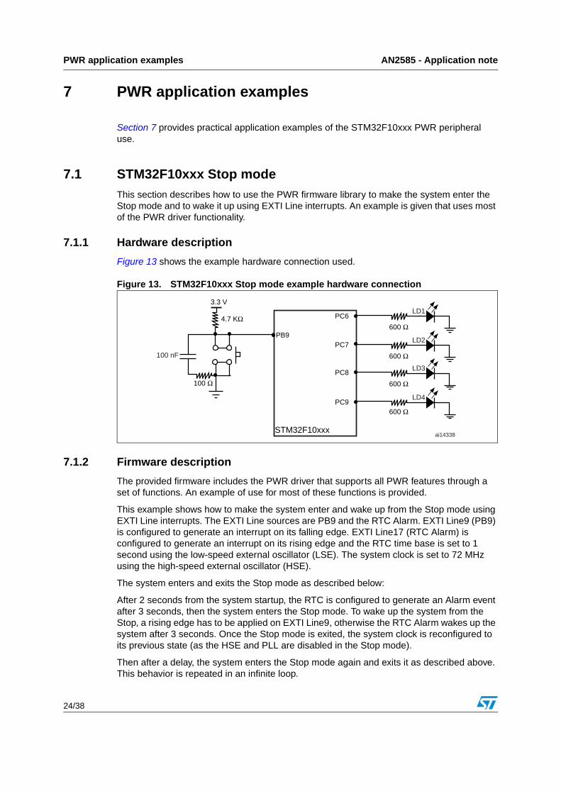
7.1.1 Hardware description
Figure 13 shows the example hardware connection used.
Figure 13. STM32F10xxx Stop mode example hardware connection
7.1.2 Firmware description
The provided firmware includes the PWR driver that supports all PWR features through a set of functions. An example of use for most of these functions is provided.
This example shows how to make the system enter and wake up from the Stop mode using EXTI Line interrupts. The EXTI Line sources are PB9 and the RTC Alarm. EXTI Line9 (PB9) is configured to generate an interrupt on its falling edge. EXTI Line17 (RTC Alarm) is configured to generate an interrupt on its rising edge and the RTC time base is set to 1 second using the low-speed external oscillator (LSE). The system clock is set to 72 MHz using the high-speed external oscillator (HSE).
The system enters and exits the Stop mode as described below:
After 2 seconds from the system startup, the RTC is configured to generate an Alarm event after 3 seconds, then the system enters the Stop mode. To wake up the system from the Stop, a rising edge has to be applied on EXTI Line9, otherwise the RTC Alarm wakes up the system after 3 seconds. Once the Stop mode is exited, the system clock is reconfigured to its previous state (as the HSE and PLL are disabled in the Stop mode).
Then after a delay, the system enters the Stop mode again and exits it as described above. This behavior is repeated in an infinite loop.
STM32F10xxx
PC7
PC9
PC6
PC8
PB9
3.3 V
4.7 KΩ
100 Ω
100 nF 600 Ω
600 Ω
600 Ω
600 Ω
ai14338
LD1
LD2
LD3
LD4

AN2585 - Application note PWR application examples
25/38
Four LEDs connected to the PC6 (LD1), PC7 (LD2), PC8 (LD3) and PC9 (LD4) pins are used to monitor the system state as follows:
LD1 on / LD4 off: system is in Run mode
LD1 off / LD4 on: system is in Stop mode
LD2 toggles if EXTI Line9 is used to exit the Stop mode
LD3 toggles if EXTI Line17 (RTC Alarm) is used to exit the Stop mode
This firmware is provided as PWR example1 in the STM32F10xxx firmware library, available from the STMicroelectronics microcontrollers website.
7.2 STM32F10xxx Standby modeThis section describes how to use the PWR firmware library to make the system enter the Standby mode and to wake it up using the external RESET, RTC Alarm or WKUP pin. An example is given that uses most of the PWR driver functionality.
7.2.1 Hardware description
Figure 14 shows the example hardware connection used.
Figure 14. STM32F10xxx Standby mode example hardware connection
STM32F10xxx
PC7
PC6
PA0
3.3 V
4.7 KΩ
100 Ω
100 nF
600 Ω
600 Ω
ai14339
PB9
3.3 V
4.7 KΩ
100 Ω
100 nF

PWR application examples AN2585 - Application note
26/38
7.2.2 Firmware description
The provided firmware includes the PWR driver that supports all PWR features through a set of functions. An example of use for most of these functions is provided.
This example shows how to make the system enter and wake up from the Standby mode using the external RESET, RTC Alarm or WKUP pin.
In the associated firmware, the system clock is set to 72 MHz, EXTI Line9 (PB9) is configured to generate an interrupt on its falling edge and SysTick is programmed to generate an interrupt every 250 ms. In the SysTick interrupt handler, the LED connected to PC6 pin is toggled to indicate whether the MCU is in Standby or Run mode.
When a falling edge is detected on EXTI Line9, an interrupt is generated. In the EXTI handler routine, the RTC is configured to generate an Alarm event after 3 seconds, then the system enters the Standby mode, causing the PC6 pin to stop toggling.
A rising edge on the WKUP pin or an external RESET will wake up the system from the Standby mode. If within 3 seconds neither of them occurs, the RTC Alarm wakes up the system.
After wakeup from the Standby mode, the program execution restarts in the same way as after a RESET, the PC6 pin restarts toggling, the PC7 pin is set to high and the RTC configuration (clock source, enable, prescaler, etc.) is unchanged. As a result, there is no need to configure the RTC.
Two LEDs connected to the PC6 (LD1) and PC7 (LD2) pins are used to monitor the system state as described below:
LD1 toggling: system is in Run mode
LD1 off / LD2 off: system is in Standby mode
LD2 on: system wakes up from Standby mode
This firmware is provided as PWR example2 in the STM32F10xxx firmware library, available from the STMicroelectronics microcontrollers website.

AN2585 - Application note BKP application examples
27/38
8 BKP application examples
Section 8 provides practical application examples of the STM32F10xxx BKP peripheral use.
8.1 How to write/read data to/from Backup data registersThis section describes how to write/read data to/from Backup data registers. An example is given that uses most of the BKP driver functionality.
8.1.1 Hardware description
Figure 15 shows an example hardware connection.
Figure 15. STM32F10xxx ANTI_TAMP connection
8.1.2 Firmware description
The provided firmware includes the BKP driver that supports all BKP features through a set of functions. An example of use for most of these functions is provided that shows how to write/read data to/from Backup data registers. It also demonstrates the Tamper detection feature.
The associated firmware performs the following:
It configures the ANTI_TAMP pin to be active low, and enables the Tamper interrupt.
It writes the data to all Backup data registers, then check whether the data were correctly written. If yes, the LED connected to PC6 turns on, otherwise the LED connected to PC7 turns on.
On applying a low level on the ANTI_TAMP pin (PC13), the Backup data registers are reset and the Tamper interrupt is generated. The corresponding ISR then checks whether the Backup data registers are cleared. If yes, the LED connected to PC8 turns on, otherwise the LED connected to PC9 is turns on.
This firmware is provided as BKP example1 in the STM32F10xxx firmware library, available from the STMicroelectronics microcontrollers website.
STM32F10xxx
PC7
PC9
PC6
PC8
PC13 (ANTI_TAMP)
3.3 V
4.7 KΩ
100 Ω
100 nF
600 Ω
600 Ω
600 Ω
600 Ω
ai14324

BKP application examples AN2585 - Application note
28/38
8.2 How to store user data into the Backup data registersThis section describes how to store user data in the Backup data registers. An example is given that uses most of the BKP driver functionality.
8.2.1 Hardware description
Figure 16 shows an example hardware connection.
Figure 16. Example connection to store user data into the Backup data registers
8.2.2 Firmware description
The provided firmware includes the BKP driver that supports all BKP features through a set of functions. An example of use for most of these functions is provided, that shows how to store user data in the Backup data registers.
As the Backup (BKP) domain is still powered by VBAT when VDD is switched off, its contentsare not lost if a battery is connected to the VBAT pin.
The program behaves as follows:
After startup the program checks if the board has been powered up. If yes, the values in the BKP data registers are checked:
– if a battery is connected to the VBAT pin, the values in the BKP data registers are retained
– if no battery is connected to the VBAT pin, the values in the BKP data registers are lost
After an external reset, the BKP data registers’ contents are not checked.
STM32F10xxx
PC7
PC9
PC6
PC8
VBAT
600 Ω
600 Ω
600 Ω
600 Ω
ai14325
3 V
LD1
LD2
LD3
LD4

AN2585 - Application note BKP application examples
29/38
Four LEDs connected to the PC6 (LD1), PC7 (LD2), PC8 (LD3) and PC9 (LD4) pins areused to monitor the system state as follows:
LD3 on / LD1 on: a Power On Reset occurred and the values in the BKP data registers are correct
LD3 on / LD2 on: a Power On Reset occurred and the values in the BKP data registers are not correct or they have not yet been programmed (if it is the first time the program is executed)
LD3 off / LD1 off / LD2 off: no Power On Reset occurred
LD4 on: program is running
This firmware is provided as BKP example2 in the STM32F10xxx firmware library, availablefrom the STMicroelectronics microcontrollers website.
RTC application examples AN2585 - Application note
30/38
9 RTC application examples
Section 9 provides practical application examples of the STM32F10xxx RTC peripheral use.
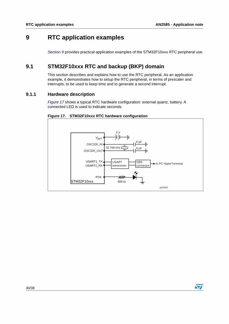
9.1 STM32F10xxx RTC and backup (BKP) domainThis section describes and explains how to use the RTC peripheral. As an application example, it demonstrates how to setup the RTC peripheral, in terms of prescaler and interrupts, to be used to keep time and to generate a second interrupt.
9.1.1 Hardware description
Figure 17 shows a typical RTC hardware configuration: external quartz, battery. A connected LED is used to indicate seconds.
Figure 17. STM32F10xxx RTC hardware configuration
STM32F10xxx
VBAT
USART1_TX
PC6
600 Ω
ai14342
USARTtransceiver
DB9connectorUSART1_RX
to PC HyperTerminal
OSC32K_IN6 pF
3 V
OSC32K_OUT6 pF32.768 kHz

AN2585 - Application note RTC application examples
31/38
9.1.2 Firmware description
The provided firmware includes the RTC driver that supports all RTC functionalities through a set of functions. An example of use for most of these functions is provided.
The low-speed external (LSE) clock is used as the RTC clock source. The RTC clock can be output on the TAMPER pin (PC13). To enable this functionality, uncomment the corresponding line: RTCClockOutput_Enable in the main.c file.
The RTC is in the backup (BKP) domain, still powered by VBAT when VDD is switched off, so the RTC configuration is not lost if a battery is connected to the VBAT pin. A key value is written in backup data register1 (BKP_DR1) to indicate if the RTC is already configured.
The program behaves as follows:
1. After startup the program checks the backup data register1 value:
– register1 value not correct: (BKP_DR1 value is not correct or has not yet been programmed when the program is executed for the first time) the RTC is configured and the user is asked to set the time (entered on HyperTerminal).
– register1 value correct: this means that the RTC is configured and the time is displayed on HyperTerminal.
2. When a External Reset occurs the BKP domain is not reset and the RTC configuration is not lost.
3. When power on reset occurs:
– If a battery is connected to the VBAT pin: the BKP domain is not reset and the RTC configuration is not lost.
– If no battery is connected to the VBAT pin: the BKP domain is reset and the RTC configuration is lost.
In the RTC interrupt service routine, the LED connected to PC6 toggles every 1 s.
The C library printf function is retargeted to the USART1, that is, the printf message is output to the HyperTerminal using USART1.
This firmware is provided as RTC example in the STM32F10xxx firmware library, available from the STMicroelectronics microcontrollers website.

Flash memory application examples AN2585 - Application note
32/38
10 Flash memory application examples
Section 10 provides practical application examples of the STM32F10xxx Flash memory use.
10.1 How to program the STM32F10xxx Flash memoryThis section describes how to use the Flash memory firmware library to program the STM32F10xxx Flash memory.
10.1.1 Firmware description
The provided firmware includes the Flash memory driver that supports all Flash memory features through a set of functions. An example of use for most of these functions is provided.
After Reset, the Flash memory Program/Erase Controller is locked. To unlock it, the FLASH_Unlock function is used.
Before programming the desired addresses, an erase operation is performed using the Flash memory Page Erase feature. The erase process starts with the calculation of the number of pages to be used. The pages to be used are then erased one by one by calling the FLASH_ErasePage function.
Once this operation is finished, the programming operation is performed by using the FLASH_ProgramWord function. The written data is then checked and the result of the programming operation is stored into the MemoryProgramStatus variable.
This firmware is provided as FLASH example 1 in the STM32F10xxx firmware library, available from the STMicroelectronics microcontrollers website.
10.2 How to enable and disable the STM32F10xxx Flash memorywrite protectionThis section describes how to use the Flash memory firmware library to enable and disable the write protection for the STM32F10xxx Flash memory.
10.2.1 Firmware description
The provided firmware includes the Flash memory driver that supports all Flash memory features through a set of functions. An example of use for most of these functions is provided.

AN2585 - Application note Flash memory application examples
33/38
10.2.2 Enable Write protection
First, uncomment the #define WriteProtection_Enable line to Enable the Write Protection.
To protect a set of pages, the user has to call the FLASH_EnableWriteProtection function.
The parameter of this function defines the number of pages to be protected. Here, eight pages from page 24 to page 31 are to be protected. The parameter therefore is: FLASH_WRProt_Pages24to27 | FLASH_WRProt_Pages28to31.
To load the new option byte values, a system Reset is necessary. The NVIC_GenerateSystemReset() function is used for that purpose.
10.2.3 Disable Write protection
First, uncomment the line #define WriteProtection_Disable to disable the writeprotection.
To disable the write protection of the STM32F10xxx Flash memory, it is necessary to erase the small information block. This operation is supported by the FLASH_EraseOptionBytes function.
To load the new option byte values, a system Reset is required. The NVIC_GenerateSystemReset() function is used for that purpose.
If the desired pages are not write-protected, they are erased and then written.
This firmware is provided as FLASH example 2 in the STM32F10xxx firmware library, available from the STMicroelectronics microcontrollers website.
How to use the STM32F10xxx IWDG AN2585 - Application note
34/38
11 How to use the STM32F10xxx IWDG
This section describes how to configure the independent watchdog (IWDG) to reload the IWDG counter at regular time intervals. An example is given that uses most of the IWDG driver functionality.
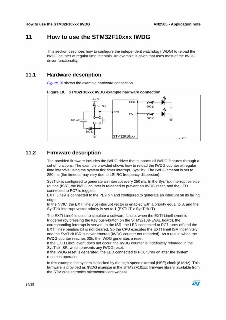
11.1 Hardware descriptionFigure 18 shows the example hardware connection.
Figure 18. STM32F10xxx IWDG example hardware connection
11.2 Firmware descriptionThe provided firmware includes the IWDG driver that supports all IWDG features through a set of functions. The example provided shows how to reload the IWDG counter at regular time intervals using the system tick timer interrupt, SysTick. The IWDG timeout is set to 280 ms (the timeout may vary due to LSI RC frequency dispersion).
SysTick is configured to generate an interrupt every 250 ms. In the SysTick interrupt service routine (ISR), the IWDG counter is reloaded to prevent an IWDG reset, and the LED connected to PC7 is toggled.EXTI Line9 is connected to the PB9 pin and configured to generate an interrupt on its falling edge.In the NVIC, the EXTI line[9:5] interrupt vector is enabled with a priority equal to 0, and the SysTick interrupt vector priority is set to 1 (EXTI IT > SysTick IT).
The EXTI Line9 is used to simulate a software failure: when the EXTI Line9 event is triggered (by pressing the Key push-button on the STM3210B-EVAL board), the corresponding interrupt is served. In the ISR, the LED connected to PC7 turns off and the EXTI line9 pending bit is not cleared. So the CPU executes the EXTI line9 ISR indefinitely and the SysTick ISR is never entered (IWDG counter not reloaded). As a result, when the IWDG counter reaches 00h, the IWDG generates a reset.If the EXTI Line9 event does not occur, the IWDG counter is indefinitely reloaded in the SysTick ISR, which prevents any IWDG reset.If the IWDG reset is generated, the LED connected to PC6 turns on after the system resumes operation.
In this example the system is clocked by the high-speed external (HSE) clock (8 MHz). This firmware is provided as IWDG example in the STM32F10xxx firmware library, available from the STMicroelectronics microcontrollers website.
STM32F10xxx
PC7
PC6
PB9
3.3 V
4.7 KΩ
100 Ω
100 nF600 Ω
600 Ω
ai14332

AN2585 - Application note How to use the STM32F10xxx WWDG
35/38
12 How to use the STM32F10xxx WWDG
This section describes how to configure the WWDG to update the WWDG counter at regular time intervals. An example is given that uses most of the WWDG driver functionality.
12.1 Hardware descriptionFigure 19 shows the example hardware connection used.
Figure 19. STM32F10xxx WWDG example hardware connection
12.2 Firmware descriptionThe provided firmware includes the WWDG driver that supports all WWDG features through a set of functions. An example of use for most of these functions is provided. The example shows how to update the WWDG counter at regular time intervals, using the early wakeup interrupt (EWI).The WWDG timeout is set to 262 ms, the refresh window is set to 41h and the EWI is enabled. When the WWDG counter reaches 40h, the EWI is generated. In the WWDG ISR, the counter is refreshed to prevent a WWDG reset and the LED connected to PC7 is toggled.
EXTI Line9 is connected to the PB9 pin, and configured to generate an interrupt on the falling edge of the signal.In the NVIC (nested vectored interrupt controller), the EXTI Line[9:5] interrupt vector is enabled with a priority equal to 0 and the WWDG interrupt vector is enabled with a priority equal to 1 (EXTI IT > WWDG IT).
EXTI Line9 is used to simulate a software failure: once the EXTI Line9 event occurs (by pressing the Key push-button on the STM3210B-EVAL board), the corresponding interrupt is served. In the ISR, the LED connected to PC7 is turned off and the EXTI Line9 pending bit is not cleared. So the CPU executes the EXTI Line9 ISR indefinitely and the WWDG ISR is never executed (the WWDG counter is not updated). As a result, when the WWDG counter falls to 3Fh, the WWDG reset occurs.
If the EXTI Line9 event does not occur, the WWDG counter is indefinitely refreshed in the WWDG ISR, and there is no WWDG reset.If the WWDG reset is generated, after the system resumes from reset, the LED connected to PC6 turns on.
STM32F10xxx
PC7
PC6
PB9
3.3 V
4.7 KΩ
100 Ω
100 nF600 Ω
600 Ω
ai14359

Conclusion AN2585 - Application note
36/38
In this example the system is clocked by HSE, the high-speed external clock (8 MHz). This firmware is provided as WWDG example in the STM32F10xxx firmware library, available from the STMicroelectronics microcontrollers website.
13 Conclusion
The examples described in this application note, provided with the STM32F10xxx firmware library, make it easer for the user to understand the product system peripherals. They also remove the user's need for dealing with peripheral low-level registers and bits.

AN2585 - Application note Revision history
37/38
14 Revision history
Table 1. Document revision history
Date Revision Changes
10-Jul-2007 1 Initial release.
09-Oct-2007 2
Internal RC frequency updated to 40 kHz instead of 32 kHz.Program modified in Section 1.1.2: Firmware description.
DMA Channel5 (not Channel1) configured to transfer the converted value of ADC_IN14 in circular mode (see Section 4.4.2: Firmware description).LSE is the RTC clock source (see Section 9.1.2: Firmware description).IWDG timeout setting modified in Section 11.2: Firmware description.

AN2585 - Application note
38/38
Please Read Carefully:
Information in this document is provided solely in connection with ST products. STMicroelectronics NV and its subsidiaries (“ST”) reserve theright to make changes, corrections, modifications or improvements, to this document, and the products and services described herein at anytime, without notice.
All ST products are sold pursuant to ST’s terms and conditions of sale.
Purchasers are solely responsible for the choice, selection and use of the ST products and services described herein, and ST assumes noliability whatsoever relating to the choice, selection or use of the ST products and services described herein.
No license, express or implied, by estoppel or otherwise, to any intellectual property rights is granted under this document. If any part of thisdocument refers to any third party products or services it shall not be deemed a license grant by ST for the use of such third party productsor services, or any intellectual property contained therein or considered as a warranty covering the use in any manner whatsoever of suchthird party products or services or any intellectual property contained therein.
UNLESS OTHERWISE SET FORTH IN ST’S TERMS AND CONDITIONS OF SALE ST DISCLAIMS ANY EXPRESS OR IMPLIEDWARRANTY WITH RESPECT TO THE USE AND/OR SALE OF ST PRODUCTS INCLUDING WITHOUT LIMITATION IMPLIEDWARRANTIES OF MERCHANTABILITY, FITNESS FOR A PARTICULAR PURPOSE (AND THEIR EQUIVALENTS UNDER THE LAWSOF ANY JURISDICTION), OR INFRINGEMENT OF ANY PATENT, COPYRIGHT OR OTHER INTELLECTUAL PROPERTY RIGHT.
UNLESS EXPRESSLY APPROVED IN WRITING BY AN AUTHORIZED ST REPRESENTATIVE, ST PRODUCTS ARE NOTRECOMMENDED, AUTHORIZED OR WARRANTED FOR USE IN MILITARY, AIR CRAFT, SPACE, LIFE SAVING, OR LIFE SUSTAININGAPPLICATIONS, NOR IN PRODUCTS OR SYSTEMS WHERE FAILURE OR MALFUNCTION MAY RESULT IN PERSONAL INJURY,DEATH, OR SEVERE PROPERTY OR ENVIRONMENTAL DAMAGE. ST PRODUCTS WHICH ARE NOT SPECIFIED AS "AUTOMOTIVEGRADE" MAY ONLY BE USED IN AUTOMOTIVE APPLICATIONS AT USER’S OWN RISK.
Resale of ST products with provisions different from the statements and/or technical features set forth in this document shall immediately voidany warranty granted by ST for the ST product or service described herein and shall not create or extend in any manner whatsoever, anyliability of ST.
ST and the ST logo are trademarks or registered trademarks of ST in various countries.
Information in this document supersedes and replaces all information previously supplied.
The ST logo is a registered trademark of STMicroelectronics. All other names are the property of their respective owners.
© 2007 STMicroelectronics - All rights reserved
STMicroelectronics group of companies
Australia - Belgium - Brazil - Canada - China - Czech Republic - Finland - France - Germany - Hong Kong - India - Israel - Italy - Japan - Malaysia - Malta - Morocco - Singapore - Spain - Sweden - Switzerland - United Kingdom - United States of America
www.st.com