an4277 application note - eefocus
TRANSCRIPT

March 2015 DocID024409 Rev 2 1/23
1
AN4277Application note
Using STM32F3 Series PWM shut-down features for motor control and digital power conversion
Introduction
The purpose of this application note is to describe STM32F3 Series timer break feature and show how it can be used with other STM32F3 Series internal resources for over-current and over-voltage protection in applications such as motor control and digital power conversion (lighting, SMPS, induction heating).
This application note:
• Provides an overview of the timer break feature,
• Details how the timer break input is connected to different break sources,
• Enumerates the different break event sources,
• Provides some scenarios of PWM output signal response to break events coming from an internal source, an external source or a combination of both internal and external break signals,
• Shows how to implement over-current and over-voltage protections using the timer break feature and other embedded peripherals (such as comparators, DAC and so on).
This document has to be read in conjunction with STM32F3 Series reference manuals:
• STM32F303xB/C/D/E, STM32F303x6/8, STM32F328x8, STM32F358xC, STM32F398xE advanced ARM®-based 32-bit MCUs (RM0316),
• STM32F302xB/C/D/E and STM32F302x6/8 advanced ARM®-based 32-bit MCUs (RM0365),
• STM32F301x6/8 and STM32F318x8 advanced ARM®-based 32-bit MCUs (RM0366),
• STM32F334xx advanced ARM®-based 32-bit MCUs (RM0364).
www.st.com

Contents AN4277
2/23 DocID024409 Rev 2
Contents
1 Break function overview . . . . . . . . . . . . . . . . . . . . . . . . . . . . . . . . . . . . . . 5
2 Break implementation . . . . . . . . . . . . . . . . . . . . . . . . . . . . . . . . . . . . . . . . 7
2.1 TIM1/8/20 break implementation . . . . . . . . . . . . . . . . . . . . . . . . . . . . . . . . 7
2.2 TIM15/16/17 break implementation . . . . . . . . . . . . . . . . . . . . . . . . . . . . . . 9
3 Break sources summary . . . . . . . . . . . . . . . . . . . . . . . . . . . . . . . . . . . . . 10
4 Examples . . . . . . . . . . . . . . . . . . . . . . . . . . . . . . . . . . . . . . . . . . . . . . . . . 11
5 Using the break function with other MCU resources . . . . . . . . . . . . . . 14
5.1 Break function used for over-current protection . . . . . . . . . . . . . . . . . . . . 14
5.2 Break function used for over-voltage protection . . . . . . . . . . . . . . . . . . . . 15
5.3 Using an external emergency signal together with the internal comparator . . . . . . . . . . . . . . . . . . . . . . . . . . . . . . . . . . . . . . . . . 16
5.4 Filtering the break input . . . . . . . . . . . . . . . . . . . . . . . . . . . . . . . . . . . . . . 18
5.5 Locking the selected configuration . . . . . . . . . . . . . . . . . . . . . . . . . . . . . . 19
Appendix A How to use the DAC to define thresholds . . . . . . . . . . . . . . . . . . . . 21
6 Revision history . . . . . . . . . . . . . . . . . . . . . . . . . . . . . . . . . . . . . . . . . . . 22
DocID024409 Rev 2 3/23
AN4277 List of tables
3
List of tables
Table 1. Peripherals availability per STM32F3 product . . . . . . . . . . . . . . . . . . . . . . . . . . . . . . . . . . . 6Table 2. Break input sources . . . . . . . . . . . . . . . . . . . . . . . . . . . . . . . . . . . . . . . . . . . . . . . . . . . . . . 10Table 3. Scenarios of PWM output status in response to internal/external break events. . . . . . . . . 11Table 4. Comparator output connected internally to break inputs . . . . . . . . . . . . . . . . . . . . . . . . . . 16Table 5. Comparator output connected externally to break inputs,
with low break polarity . . . . . . . . . . . . . . . . . . . . . . . . . . . . . . . . . . . . . . . . . . . . . . . . . . . . 17Table 6. Comparator output connected externally to break inputs,
with high break polarity . . . . . . . . . . . . . . . . . . . . . . . . . . . . . . . . . . . . . . . . . . . . . . . . . . . 17Table 7. Register locking mechanism. . . . . . . . . . . . . . . . . . . . . . . . . . . . . . . . . . . . . . . . . . . . . . . . 20Table 8. Document revision history . . . . . . . . . . . . . . . . . . . . . . . . . . . . . . . . . . . . . . . . . . . . . . . . . 22

List of figures AN4277
4/23 DocID024409 Rev 2
List of figures
Figure 1. Break feature implementation for TIM1, TIM8 and TIM20 . . . . . . . . . . . . . . . . . . . . . . . . . . 7Figure 2. Break feature implementation for TIM15, TIM16 and TIM17 . . . . . . . . . . . . . . . . . . . . . . . . 9Figure 3. Over-current protection network implemented with STM32F3 Series . . . . . . . . . . . . . . . . 14Figure 4. Over-voltage protection network implemented with STM32F3 Series . . . . . . . . . . . . . . . . 15Figure 5. Combining external and internal protection concept. . . . . . . . . . . . . . . . . . . . . . . . . . . . . . 18Figure 6. Comparator chain configuration locking . . . . . . . . . . . . . . . . . . . . . . . . . . . . . . . . . . . . . . . 19Figure 7. Inverting input selection . . . . . . . . . . . . . . . . . . . . . . . . . . . . . . . . . . . . . . . . . . . . . . . . . . . 21

DocID024409 Rev 2 5/23
AN4277 Break function overview
22
1 Break function overview
The break function is available in TIM1, TIM8, TIM20, TIM15, TIM16 and TIM17 timers. These timers are able to generate complementary PWM signals with deadtime insertion for driving powers switches in half bridge topology.
The purpose of the break function is to protect power switches driven by PWM signals generated with these timers. When triggered by a fault, the break circuitry shuts down the PWM outputs and forces them to a predefined safe state.
For TIM1/8/20, there are three break inputs (BRK, BRK_ACTH and BRK2), while in TIM15/16/17 two break inputs (BRK and BRK_ACTH) are available.
The BRK input can either disable the PWM outputs (inactive state) or forces them to a predefined safe state, either active or inactive, after a dead time insertion which allows to prevent any shoot-through in the half bridge. The BRK2 only disables the PWM outputs (inactive state).
BRK has higher priority than BRK2. When both protections are triggered, the predefined safe state related to BRK circuitry overrides the inactive state related to the BRK2 input.
Typically, a permanent magnet 3-phase brushless motor drive will use the protections as follows:
• the BRK2 input as an over-current protection, opening the 6 switches from the power stage,
• the BRK input for over-voltage protection, overriding the over-current and closing the 3 low-side switches to avoid current regeneration to build up bus voltage and exceed capacitors rated voltage.
As an example, for a dual motor drive, comparators 1, 2 and 3 can be affected to over-current monitoring of the 3 phases of motor 1 (BRK2 input of TIM1). Comparators 4, 5 and 6 can be affected to over-current monitoring of the 3 phases of motor 2 (BRK2 input of TIM8), while comparator 7 will be used for over-voltage monitoring (driving BRK inputs of both TIM1 and TIM8).
BRK_ACTH input is connected only to internal signals like CSS, PVD output and so on. For more details, refer to Section 2: Break implementation.

Break function overview AN4277
6/23 DocID024409 Rev 2
The availability of peripherals impacting the break feature depends on the selected STM32F3 product. This is summarized in Table 1.
Table 1. Peripherals availability per STM32F3 product
ST
M32
F30
3xD
/E
ST
M32
F39
8xE
ST
M32
F30
3xB
/C
ST
M32
F35
8xC
ST
M32
F30
3x6
/8
ST
M32
F32
8x8
ST
M32
F30
2xD
/E
ST
M32
F30
2xB
/C
ST
M32
F30
2x6
/8
ST
M32
F30
1x6
/8
ST
M32
F31
8x8
ST
M32
F33
4x4
/6/8
COMP1 X X - X X - -
COMP2 X X X X X X X
COMP3 X X - - - - -
COMP4 X X X X X X X
COMP5 X X - - - - -
COMP6 X X X X X X X
COMP7 X X - - - - -
TIM1 X X X X X X X
TIM8 X X - - - - -
TIM15 X X X X X X X
TIM16 X X X X X X X
TIM17 X X X X X X X
TIM20 X - - - - - -

DocID024409 Rev 2 7/23
AN4277 Break implementation
22
2 Break implementation
2.1 TIM1/8/20 break implementation
For the advanced-control timers TIM1, TIM8 and TIM20, there are three break inputs:
• BRK,
• BRK_ACTH,
• BRK2.
Figure 1 shows the break feature implementation for TIM1, TIM8 and TIM20.
Figure 1. Break feature implementation for TIM1, TIM8 and TIM20

Break implementation AN4277
8/23 DocID024409 Rev 2
BRK
The input signal on BRK is a logical OR between the input signal on BKIN pin and the used comparator (4 or 7) output if configured.
If BKIN alternate function is disabled, the resulting break signal is the comparator (4 or 7) output.
Polarity selection and filter features are available when BRK is used.
BRK_ACTH
This input only gathers internal signals, and can be connected to comparators (1, 2, 3, 5 and 6) outputs, CSS, PVD output, SRAM parity error and Hardfault. When this input is used, the polarity selection and filter features are not available. It is always active high. BRK_ACTH is enabled using the same bit as BRK (BKE in TIMx_BDTR, x=1, 8, 20).
When using BRK_ACTH as break input, the polarity must be configured High. Otherwise, there will be no PWM generation independently of the break signal coming from the internal source.
If there are several break input sources, the resulting input signal will be an OR between all the input signals.
In the particular case where there is an internal break input signal connected to BRK_ACTH and an external input signal coming through the BKIN pin (BKIN alternate function is enabled), the resulting break input signal will be an OR between the signal on BKIN and the internal break signal.
BRK2
Only comparators outputs can be connected internally to BRK2. Other outputs such as CSS and PVD can not be connected internally to BRK2.
The input signal on BRK2 is a logical OR between the input signal on BKIN2 pin and the selected comparators outputs (COMP1, 2, 3, 4, 5, 6, 7). If BKIN2 alternate function is disabled (input not used), the resulting break signal is solely related to the comparators.
Polarity selection and filter features are available when BRK2 is used.

DocID024409 Rev 2 9/23
AN4277 Break implementation
22
2.2 TIM15/16/17 break implementation
For TIM15, TIM16 and TIM17 there are two break inputs:
• BRK,
• BRK_ACTH.
Figure 2 shows the break feature implementation for TIM15, TIM16 and TIM17.
Figure 2. Break feature implementation for TIM15, TIM16 and TIM17
BRK
• The input signal on BRK is the input signal on BKIN.
• Polarity selection and filter features are available when BRK is used.
BRK_ACTH
• This input gathers internal signals and can be connected to comparator x (x = 3, 5, 7) output, CSS, PVD output, SRAM parity error and Hardfault. The Comparator x output (x = 3, 5, 7) is internally connected to TIMy (y = 15,16,17) BRK_ACTH input, depending on the COMPxOUTSEL bits in the comparator x control register.
• When using BRK_ACTH as break input, the polarity selection and filter features are not available.
• BRK_ACTH is enabled using the same bit as BRK (BKE in TIMx_BDTR, x=15,16,17).
Consequently:
• If only an internal break source is used, the polarity must be configured to “High” in the software.
• If there are several break input sources, the resulting input signal will be an OR between all the input signals.
• If both internal break source and BKIN are used, the resulting break signal will be an OR between the signal on BKIN pin and the internal break signal.

Break sources summary AN4277
10/23 DocID024409 Rev 2
3 Break sources summary
Table 2 summarizes the available break sources and their connections externally or internally to timers (1, 8, 20, 15, 16 and 17) break inputs.
Table 2. Break input sources
BRK BRK_ACTH BRK2
External connection to pin BKIN No corresponding I/O BKIN2
Internal connection toComparators 4 and 7 for TIM1/8/20
NA for TIM15/16/17
– Clock failure event generated by CSS
– Comparators 1, 2, 3, 5 and 6 for TIM1/8/20 and Comparators 3, 5 and 7 for respectively TIM15, 16 and 17
– PVD output
– RAM parity error signal
– Cortex®-M4 LOCKUP output (Hardfault)
Comparators 1, 2, 3, 4, 5, 6 and 7
Polarity feature in case of internal connection
Configurable: active high or active low
Always active highConfigurable: active high or active low
Filter feature in case of internal connection
Filter feature is available
Filter feature is NOT available Filter feature is available
Polarity feature in case of external break event
Available NA Available
Filter feature in case of external break event
Available NA Available
Available in TIM1/8/20/15/16/17 TIM1/8/20/15/16/17 TIM1/8/20
Resulting break signal in case of parallel external or/and internal break sources
It is an OR between the external break signal(s) and the internal one(s)

DocID024409 Rev 2 11/23
AN4277 Examples
22
4 Examples
Table 3 shows the PWM output status for TIMx (where x = 1, 8, 20, 15, 16, 17) in response to internal/external break events.
In the following waveforms:
• “PWM” signal is the reference PWM waveform (internal signal, before BRK protection).
• “COMP_OUT” signal represents the BRK input signal, in our case it is the comparator output.
• “BKIN” signal is the input signal on BKIN.
• “PWM_BRK” signal is the resulting PWM signal on the timer output after break detection.
Color legend for Table 3: green = PWM signal, red = COMP_OUT signal, blue = BKIN signal, purple = PWM_BRK signal.
I
Table 3. Scenarios of PWM output status in response to internal/external break events
ConfigurationProgrammed
polarityResult
Comparator 1 output is connected internally to TIM1 BRK_ACTH and TIM1 BKIN alternate function is disabled.
High
The PWM generation is stopped when the comparator output is at the high level, as shown in the following screen shot:

Examples AN4277
12/23 DocID024409 Rev 2
Comparator 1 output is connected internally to TIM1 BRK_ACTH and TIM1 BKIN alternate function is enabled.
High/Low
The break input signal is an OR between the signal on BKIN and the comparator output. The following screen shot shows an example (polarity = High):
Note: In order to show the effect of the two break sources, the bit AOE in BDTR register is set, allowing to re-start the PWM at the next update event.
Table 3. Scenarios of PWM output status in response to internal/external break events (continued)
ConfigurationProgrammed
polarityResult

DocID024409 Rev 2 13/23
AN4277 Examples
22
Comparator 4 output is connected internally to TIM1 BRK and filter is not configured.
Low
The PWM signal is stopped during the break signal low level, as shown in the following screen shot:
Comparator 4 output is connected internally to TIM1 BRK and filter is configured.
High
During the window defined by the filter duration, the break event has no impact on the PWM generation even if the break condition is verified.
This is the case of the following example (screen shot) where the PWM signal is generated normally when the break signal is at high level during the window defined by the filter.
– The filter duration is 666 ns (BKF = 1000b, Filter duration is (6*8/fDTS), fDTS = 72 MHz).
– The comparator output high level duration is 1.207 µs.
Table 3. Scenarios of PWM output status in response to internal/external break events (continued)
ConfigurationProgrammed
polarityResult

Using the break function with other MCU resources AN4277
14/23 DocID024409 Rev 2
5 Using the break function with other MCU resources
5.1 Break function used for over-current protection
The STM32F3 Series microcontroller embeds a set of peripherals designed to resolve common motor control issues by reducing the number of required external components. This section describes how to use these peripherals to implement over-current protection. Figure 3 shows the over-current protection network that can be implemented using the internal resources of the STM32F3 Series.
Figure 3. Over-current protection network implemented with STM32F3 Series
The principle of this over-current protection mechanism can be summarized as follows:
• The phase current of the motor flows in the power transistor of the inverter bridge and passes through the shunt resistor (RShunt) producing a voltage drop (V+).
• This voltage drop is compared with a threshold (V-) defining the maximum admissible current.
• If the threshold is exceeded, a break signal stops the PWM generation putting the system in a safe state.
All of these actions can be performed using the internal resources of the STM32F3 Series and, in particular, the embedded comparators and advanced timer break function (BRK2). In the basic implementation, the only external component required is the shunt resistor that must be sized depending on the current to be monitored and the shunt resistor power rating.
DocID024409 Rev 2 15/23
AN4277 Using the break function with other MCU resources
22
The two dotted line boxes in Figure 3 show the components required to measure current:
• The R1/R2 resistive network to add an offset necessary to measure AC currents.
• An operational amplifier with a built-in gain setting network.
The amplification network can be implemented externally for specific use cases where the built-in gain settings are not adequate.
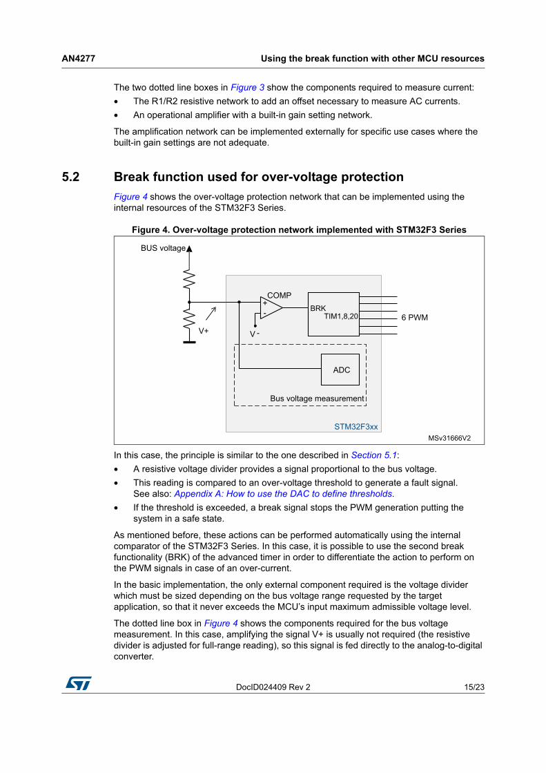
5.2 Break function used for over-voltage protection
Figure 4 shows the over-voltage protection network that can be implemented using the internal resources of the STM32F3 Series.
Figure 4. Over-voltage protection network implemented with STM32F3 Series
In this case, the principle is similar to the one described in Section 5.1:
• A resistive voltage divider provides a signal proportional to the bus voltage.
• This reading is compared to an over-voltage threshold to generate a fault signal. See also: Appendix A: How to use the DAC to define thresholds.
• If the threshold is exceeded, a break signal stops the PWM generation putting the system in a safe state.
As mentioned before, these actions can be performed automatically using the internal comparator of the STM32F3 Series. In this case, it is possible to use the second break functionality (BRK) of the advanced timer in order to differentiate the action to perform on the PWM signals in case of an over-current.
In the basic implementation, the only external component required is the voltage divider which must be sized depending on the bus voltage range requested by the target application, so that it never exceeds the MCU’s input maximum admissible voltage level.
The dotted line box in Figure 4 shows the components required for the bus voltage measurement. In this case, amplifying the signal V+ is usually not required (the resistive divider is adjusted for full-range reading), so this signal is fed directly to the analog-to-digital converter.

Using the break function with other MCU resources AN4277
16/23 DocID024409 Rev 2
5.3 Using an external emergency signal together with the internal comparator
Commonly in MC applications, gate driver ICs - such as ST’s L639x family - or Intelligent Power Modules (IPMs) - such as ST’s “SLLIMM” (Small Low-Loss Intelligent Molded Module) family - have integrated comparators that can protect the inverter (ST’s “Smart Shutdown” function) while sending an error signal to the microcontroller.
In this section, we will see that it is possible to combine these two concepts, as shown in Figure 5, so as to enhance by redundancy the functional safety offered by the “break function”.
A first option is when the break function is triggered by internal comparators output only: the error signal coming from ICs or IPMs should not be connected to the microcontroller, thus saving the pin. The configuration to be set in this case is summarized in the following table:
On the contrary, the user may prefer to make use of the external error signal in conjunction with the internal one: the result is an OR between the two. Depending on the external comparator logic, the possible configurations to be written are summarized in the following tables:
Table 4. Comparator output connected internally to break inputs
Description Register Bit Configuration
TIM1/8/20 BRK_ACTH/BRK/BRK2 polarity
TIMx_BDTR BKP or BK2P 1 (active high)
Comparator output polarity COMPx_CSR COMPxPOL0 (not inverted), comparators input connected as shown in previous sections
TIM1/8/20 BKIN and BKIN2 AFGPIOxAFRL or GPIOxAFRH
- AF not enabled on BKIN1/2 related pins
TIM1/8/20 BRK and BRK2 enable
TIMX_BDTR BKE or BK2E 1
COMPx out selection COMPx_CSR COMPxOUTSEL
0001: TIM1 BRK or TIM1 BRK_ACTH(1)
0010: TIM1 BRK2
0011: TIM8 BRK or TIM8 BRK_ACTH(2)
0100: TIM8 BRK2
0101: TIM1 BRK2 + TIM8 BRK2
1100: TIM20 BRK or TIM20 BRK_ACTH(3)
1101: TIM20 BRK2
1110: TIM1 BRK2 + TIM8 BRK2 + TIM20 BRK2
1. TIM1 BRK in case of COMP4 and COMP7, or TIM1 BRK_ACTH in case of COMPx, x = 1, 2, 3, 5 and 6.
2. TIM8 BRK in case of COMP4 and COMP7, or TIM8 BRK_ACTH in case of COMPx, x = 1, 2, 3, 5 and 6.
3. TIM20 BRK in case of COMP4 and COMP7, or TIM20 BRK_ACTH in case of COMPx, x= 1, 2, 3, 5 and 6.

DocID024409 Rev 2 17/23
AN4277 Using the break function with other MCU resources
22
Comparators output can be optionally enabled as alternate function on the related GPIO pin, in push-pull or open-drain mode, for signaling to other devices or for debugging purposes.
Table 5. Comparator output connected externally to break inputs, with low break polarity
Description Register Bit Configuration
TIM1/8/20 BRK polarity TIMx_BDTR BKP0 (active low), it means that the external signal goes low during the fault
Comparator output polarity COMPx_CSR COMPxPOL0 (not inverted), comparators input connected as shown in previous sections
TIM1/8/20 BKIN AFGPIOxAFRL or GPIOxAFRH
-AF enabled on BKIN pin selected among available
TIM1/8/20 BRK enable TIMX_BDTR BKE 1
COMPx out selection COMPx_CSR COMPxOUTSEL
0001: TIM1 BRK
0011: TIM8 BRK
1100: TIM20 BRK
Table 6. Comparator output connected externally to break inputs, with high break polarity
Description Register Bit Configuration
TIM1/8/20 BRK/BRK2 polarity TIMx_BDTR BKP or BK2P1 (active high), it means that the external signal goes high during the fault
Comparator output polarity COMPx_CSR COMPxPOL0 (not inverted), comparators input connected as shown in previous sections
TIM1/8/20 BKIN/BKIN2 AFGPIOxAFRL or GPIOxAFRH
-AF enabled on BKIN/BKIN2 pin selected among available
TIM1/8/20 BRK/BRK2 enable TIMX_BDTR BKE or BK2E 1
COMPx out selection COMPx_CSR COMPxOUTSEL
0001: TIM1 BRK
0010: TIM1 BRK2
0011: TIM8 BRK
0100: TIM8 BRK2
0101: TIM1 BRK2 + TIM8 BRK2
1100: TIM20 BRK
1101: TIM20 BRK2
1110: TIM1 BRK2 + TIM8 BRK2 + TIM20 BRK2

Using the break function with other MCU resources AN4277
18/23 DocID024409 Rev 2
Figure 5. Combining external and internal protection concept
5.4 Filtering the break input
Programmable filters are available to prevent break functions of advanced timers from being triggered on spurious events (switching noise for instance).
The digital filter feature is available on BRK and BRK2. It is not available on BRK_ACTH.
That means that the digital filter is:
• available when the break source is external and comes from the external inputs BKIN/BKIN2,
• available when the break source is internal and connected to BRK or BRK2,
• not available when the break source is internal and connected to BRK_ACTH.

DocID024409 Rev 2 19/23
AN4277 Using the break function with other MCU resources
22
5.5 Locking the selected configuration
Electrical motor drives require high level of reliability and robustness for the potential damages that may be caused in case of failure.
To increase robustness against software runaways, the STM32F3 Series microcontroller comes with a chain of peripherals featuring the lock feature, beginning from the mode of the GPIO pins used for sensing through comparators, operational amplifiers (opamp) and advanced timers, down to the GPIO pins used for driving, as shown in Figure 6.
In particular, BRK and BRK2 configuration can be locked using the LOCK bits in TIMx_BDTR register. At least LOCK level 1 is recommended to freeze DTG/BKE/BKP/AOE/BKF/BK2F/BK2E/BK2P bits in TIMx_BDTR register and OISx/OISxN bits in TIMx_CR2 register until next reset.
Figure 6. Comparator chain configuration locking
Using the break function with other MCU resources AN4277
20/23 DocID024409 Rev 2
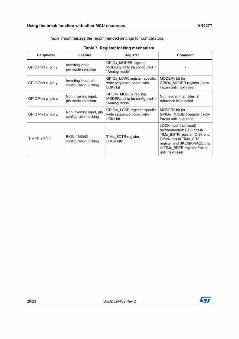
Table 7 summarizes the recommended settings for comparators.
Table 7. Register locking mechanism
Peripheral Feature Register Comment
GPIO Port x, pin yInverting input, pin mode selection
GPIOx_MODER register, MODERy bit to be configured in “Analog mode”
-
GPIO Port x, pin yInverting input, pin configuration locking
GPIOx_LCKR register, specific write sequence coded with LCKy bit
MODERy bit (in GPIOx_MODER register ) now frozen until next reset
GPIO Port w, pin zNon inverting input, pin mode selection
GPIOw_MODER register, MODERz bit to be configured in “Analog mode”
Not needed if an internal reference is selected
GPIO Port w, pin zNon inverting input, pin configuration locking
GPIOw_LCKR register, specific write sequence coded with LCKz bit
MODERz bit (in GPIOw_MODER register ) now frozen until next reset
TIMER 1/8/20BKIN / BKIN2 configuration locking
TIMx_BDTR register, LOCK bits
LOCK level 1 (at least) recommended: DTG bits in TIMx_BDTR register, OISx and OISxN bits in TIMx_CR2 register and BKE/BKP/AOE bits in TIMx_BDTR register frozen until next reset

DocID024409 Rev 2 21/23
AN4277 How to use the DAC to define thresholds
22
Appendix A How to use the DAC to define thresholds
Concerning the network shown in Figure 3 and Figure 4, it is important to properly set the comparator inverting input voltage (V-) to define the threshold levels for over-current protection and over-voltage protection.
As shown in Figure 7 below, in the STM32F3 Series microcontroller it is possible to set three different sources as inverting input for the comparator:
• An external reference (GPIO),
• A fixed internal reference (Vref, ¾ Vref, ½ Vref, ¼ Vref),
• A programmable internal reference (DAC).
Figure 7. Inverting input selection
Practical example: Over-current protection using the offset network
This is the case of Figure 3 when the components inside the dotted line boxes are present. In this case, the formula to compute the over-current threshold is the following:
Equation 1
Usually the R1 and R2 values are used to satisfy the current measurement needs. It is clear that using the internal reference for V- can lead to a threshold value Ith which is not exactly coincident with the required one. As explained in this practical example, the internal reference can be used only when there is no need to fine-tune the over-current threshold. Otherwise, it is necessary to use the external reference or the variable internal reference. The latter is recommended, because it does not require any external components.
The STM32F3 Series microcontroller includes two 12-bit DAC channels that can be used for this purpose. For three-phase motor drives, it is possible to group three comparators to protect each leg of the inverter bridge versus over-current by setting the same DAC channel for all three inverter inputs.
The same can be done in case of dual motor control with also having the possibility to define two different levels of protection, one for each motor.
Ith
V-
Vdd
R2
R1 R2+--------------------×⎝ ⎠
⎛ ⎞–
Rshunt
R1
R1 R2+--------------------⎝ ⎠
⎛ ⎞×-------------------------------------------------------=

Revision history AN4277
22/23 DocID024409 Rev 2
6 Revision history
Table 8. Document revision history
Date Revision Changes
25-Nov-2013 1 Initial release.
05-Mar-2015 2
Updated cover page with STM32F3 Series and adding RM references.
Updated the whole document adding TIM20 and replacing STM32F30x/31 x by STM32F3 Series.
Updated Section 1: Break function overview adding Table 1: Peripherals availability per STM32F3 product.
Updated Figure 1: Break feature implementation for TIM1, TIM8 and TIM20.
Updated Figure 6: Comparator chain configuration locking.
Updated Table 7: Register locking mechanism.
DocID024409 Rev 2 23/23
AN4277
23
IMPORTANT NOTICE – PLEASE READ CAREFULLY
STMicroelectronics NV and its subsidiaries (“ST”) reserve the right to make changes, corrections, enhancements, modifications, and improvements to ST products and/or to this document at any time without notice. Purchasers should obtain the latest relevant information on ST products before placing orders. ST products are sold pursuant to ST’s terms and conditions of sale in place at the time of order acknowledgement.
Purchasers are solely responsible for the choice, selection, and use of ST products and ST assumes no liability for application assistance or the design of Purchasers’ products.
No license, express or implied, to any intellectual property right is granted by ST herein.
Resale of ST products with provisions different from the information set forth herein shall void any warranty granted by ST for such product.
ST and the ST logo are trademarks of ST. All other product or service names are the property of their respective owners.
Information in this document supersedes and replaces information previously supplied in any prior versions of this document.
© 2015 STMicroelectronics – All rights reserved