an4924 application note - stmicroelectronics · october 2016 docid029815 rev 1 1/35 an4924...
TRANSCRIPT

October 2016 DocID029815 Rev 1 1/35 www.st.com
AN4924 Application note
12 V, 8.4 W peak power 30 W isolated flyback converter using VIPer38HD
Introduction The STEVAL-ISA182V1 is a 12 V/8.4 W power supply set in isolated flyback topology using the new VIPer38HD, an off-line high voltage converter by STMicroelectronics, which can be used as an external adapter or as an auxiliary power supply in consumer equipment.
The VIPer38HD has the following main characteristics:
• 800 V avalanche rugged power section• PWM operation at 115 kHz with jittering frequency for lower EMI• cycle-by-cycle current limit with adjustable set point• on-board soft-start• safe auto-restart after a fault condition• possible management of an extra output power for a fixed time (set by a capacitor connected to the
EPT pin).
The available protections are:
• thermal shutdown with hysteresis• two levels of overcurrent protection• overvoltage protection• overload protection.
Figure 1: STEVAL-ISA182V1 evaluation board (top view)
Figure 2: STEVAL-ISA182V1 evaluation board (bottom view)

Contents AN4924
2/35 DocID029815 Rev 1
Contents 1 Adapter features .............................................................................. 52 Circuit description ........................................................................... 63 Schematic diagram and bill of materials ....................................... 74 Transformer ................................................................................... 105 Testing the board .......................................................................... 11
5.1 Efficiency ......................................................................................... 11
5.2 Output voltage characteristics ......................................................... 12
5.3 No load consumption ...................................................................... 14
5.4 Light load consumption ................................................................... 15
6 Extra power time management function (EPT) ............................ 167 Typical waveforms ........................................................................ 18
7.1 Dynamic step load regulation .......................................................... 22
8 Soft start ........................................................................................ 249 Protection features ........................................................................ 25
9.1 Overload and short-circuit protection .............................................. 25
9.2 Overvoltage protection .................................................................... 26
9.3 2nd level overcurrent protection ....................................................... 28
10 Conducted noise measurements ................................................. 3011 Thermal measurements ................................................................ 3112 Conclusions ................................................................................... 3313 Revision history ............................................................................ 34

AN4924 List of tables
DocID029815 Rev 1 3/35
List of tables Table 1: STEVAL-ISA182V1 electrical specifications ................................................................................. 5 Table 2: Bill of materials.............................................................................................................................. 8 Table 3: Transformer characteristics ........................................................................................................ 10 Table 4: EC CoC version 5 energy-efficiency criteria for active mode (excluding low voltage external power supplies), Tier 2 (1 January 2016) ................................................................................................. 11 Table 5: EC CoC version 5 energy-efficiency criteria for active mode (excluding low voltage external power supplies) at 10% maximum output load, Tier 2 (1 January 2016) ................................................. 11 Table 6: STEVAL-ISA182V1 average efficiency at 115 VAC ..................................................................... 11 Table 7: STEVAL-ISA182V1 average efficiency at 10% of the max. output load .................................... 11 Table 8: Output voltage line-load regulation ............................................................................................. 12 Table 9: Key component temperature (TAMB = 25 °C, emissivity = 0.95 for all points) ............................. 32 Table 10: Document revision history ........................................................................................................ 34

List of figures AN4924
4/35 DocID029815 Rev 1
List of figures Figure 1: STEVAL-ISA182V1 evaluation board (top view) ......................................................................... 1 Figure 2: STEVAL-ISA182V1 evaluation board (bottom view) ................................................................... 1 Figure 3: STEVAL-ISA182V1 schematic diagram ...................................................................................... 7 Figure 4: Dimensional drawing and pin placement diagram (bottom view) .............................................. 10 Figure 5: Dimensional drawing and pin placement diagram (electrical diagram) ..................................... 10 Figure 6: Dimensional drawing and pin placement diagram (side view) .................................................. 10 Figure 7: Efficiency vs. output current load............................................................................................... 12 Figure 8: Output voltage load regulation at 115 VAC ................................................................................. 13 Figure 9: No load consumption vs. input voltage ...................................................................................... 14 Figure 10: Light load consumption at different output power.................................................................... 15 Figure 11: Extra power management ....................................................................................................... 16 Figure 12: Extra power condition at 85 VAC .............................................................................................. 17 Figure 13: Extra power condition at 115 VAC ............................................................................................ 17 Figure 14: Waveforms at 85 VAC (min. input voltage), full load ................................................................ 18 Figure 15: Waveforms at 132 VAC (max. input voltage), full load ............................................................. 19 Figure 16: Waveforms at 115 VAC (nominal input voltage), full load ......................................................... 19 Figure 17: Output voltage ripple at 115 VAC, burst condition .................................................................... 20 Figure 18: Output voltage ripple at 115 VAC, full load ............................................................................... 21 Figure 19: Dynamic step load at 115 VAC (IOUT from 0 to 0.7 A) ............................................................... 22 Figure 20: Dynamic step load at 115 VAC (IOUT from 0 to 2.5 A) ............................................................... 23 Figure 21: Soft start .................................................................................................................................. 24 Figure 22: Overload: OLP triggering ......................................................................................................... 25 Figure 23: Overload: continuous ............................................................................................................... 26 Figure 24: Overvoltage event ................................................................................................................... 27 Figure 25: Overvoltage magnification ....................................................................................................... 27 Figure 26: 2nd level overcurrent event ..................................................................................................... 28 Figure 27: 2nd level overcurrent event magnification ............................................................................... 29 Figure 28: CE average measurements at 115 VAC, full load .................................................................... 30 Figure 29: Thermal measurements at 115 VAC, full load, top layer .......................................................... 31 Figure 30: Thermal measurements at 115 VAC, full load, bottom layer .................................................... 31

AN4924 Adapter features
DocID029815 Rev 1 5/35
1 Adapter features Table 1: STEVAL-ISA182V1 electrical specifications
Parameter Min. Typ. Max. Unit
AC main input voltage 85 132 VAC
Main frequency (fL) 50 60 Hz
Output voltage 11.4 12 12.6 V
Output current 0.7 A
Rated output power 8.4 W
Output ripple voltage 50 mV
Output peak current 2.5 A
Output peak power 30 W
Duration output peak power 10 ms
Output voltage during peak power 9 12.6 V
Standby input power at 115 VAC 25 mW
Active mode efficiency 81.14 %
Active mode efficiency at 10% nameplate O/P 71.14 %
Ambient operating temperature 60 ºC

Circuit description AN4924
6/35 DocID029815 Rev 1
2 Circuit description The power supply is set in isolated flyback topology.
The input section includes a diode bridge (BR), a π filter (C2, L1, C3), an X-capacitor (C1) for differential EMC suppression and a CM choke for common mode EMC suppression.
A clamp network (D1, R1, C4) is used for leakage inductance demagnetization.
The resistor connected between CONT pin and ground lowers the device default current limitation (according to the IDLIM vs RLIM graphic reported in the datasheet) to the desired power throughput value, thus avoiding unnecessary power component overstress.
A small LC filter has been added to the output to filter the high frequency ripple.

AN4924 Schematic diagram and bill of materials
DocID029815 Rev 1 7/35
3 Schematic diagram and bill of materials Figure 3: STEVAL-ISA182V1 schematic diagram
C9
820u
F
D4
BAT4
1ZFI
LM
D1
STT
H1L
06A
R6
47k
C10
220u
F
R9
240k
D5
18V
T1
OPT
O
SFH
610A
320V
RV
C11
1uF
RE
F
TS43
2
R8
150k
C1
220n
F
C14
47nF
R11
15k
FS 2 A
OPT
OS
FH61
0A
L1
1mH
R2
4.7
C4
220p
F
C2
22uF
C7
10nF
IC1
VIP
ER
38H
EPT
CO
NT
DR
AIN
GN
D
CO
NTR
OL
VD
D
FB
R12
2.2M
C5
220p
F
R10
130k
R1
220k
C8
33nF
CM
20m
H
2 1
3 4D
2
BAT4
1ZFI
LMR
3
130kD
3
BAT4
1ZFI
LM
BR
-+
C13
2.2n
F
L2
3.3u
H
R5
220
C12
10nF
C6
33uF
D6
STP
S5H
100B
C3
22uF
R7
1k
R4
30k
12V-
0.7A
GN
D
AC
INA
C IN
GSPG190716 1120SG

Schematic diagram and bill of materials AN4924
8/35 DocID029815 Rev 1
Table 2: Bill of materials Reference Order code Manufacturer Description
BR DBLS105G Taiwan Semiconductors 1 A – 600 V bridge
RV B72210S0321K101 EPCOS 320 V varistor
FS 0461002.ER Littlefuse 2 A fuse
R1 CRGH1206J220K TE Connectivity 220 kΩ ± 5% - 0.5 W resistor
R2 ERJ3BQF4R7V Panasonic 4.7 Ω ± 1% - 0.2 W resistor
R3 ERJ3EKF1303V Panasonic 130 kΩ ± 1% - 0.1 W resistor
R4 ERJU03F3002V Panasonic 30 kΩ ± 1% - 0.1 W resistor
R5 ERJT06J221V Panasonic 220 Ω ± 5% - 0.25 W resistor
R6 ERJ-3EKF4702V Panasonic 47 kΩ ± 1% - 0.1 W resistor
R7 ERJ3GEYJ102V Panasonic 1 kΩ ± 5% - 0.1 W resistor
R8 ERJ3GEYJ154V Panasonic 150 kΩ ± 5% - 0.1 W resistor
R9 ERJ3GEYJ244V Panasonic 240 kΩ ± 5% - 0.1 W resistor
R10 ERJP03F1303V Panasonic 130 kΩ ± 1% - 0.2 W resistor
R11 ERJP03F1502V Panasonic 15 kΩ ± 1% - 0.2 W resistor
R12 ERJ3GEYJ225V Panasonic 2.2 MΩ ± 5% - 0.1 W resistor
C1 BFC233920224 Vishay 220 nF - 275 V X2 capacitor
C2, C3 250BXC22MEFC10X16 Rubycon 22 μF - 250 V electrolytic capacitor
C4 C3216C0G2J221J060AA TDK 220 pF - 630 V capacitor
C5 GRM188R71H221KA01D Murata 220 pF - 50 V capacitor
C6 35YXM33MEFC5X11 Rubycon 33 μF - 35 V electrolytic capacitor
C7 GRM188R71H103KA01D Murata 10 nF - 50 V capacitor
C8 GRM188R71H333KA61D Murata 33nF - 50 V capacitor
C9 25ZLK820M10X20 Rubycon 820 μF - 25 V electrolytic capacitor
C10 25PK220MEFC6.3X11 Rubycon 220 μF - 25 V electrolytic capacitor
C11 GRM188C81E105KAADD Murata 1 μF - 25 V capacitor
C12 GRM188R71H103KA01D Murata 10 nF - 50 V capacitor
C13 DE2E3KY222MA2BM01 Murata 2.2 nF – 250 V X1/Y2 capacitor
C14 GRM188F51H473ZA01D Murata 47 nF – 50 V capacitor
D1 STTH1L06A STMicroelectronics 1 A – 600 V ultrafast diode
D2, D3, D4 BAT41ZFILM STMicroelectronics 0.2 A - 100 V signal Schottky
D5 MMSZ5248BT1G ONSemiconductor 18 V Zener diode
D6 STPS5H100B STMicroelectronics 100 V-5 A Power Schottky

AN4924 Schematic diagram and bill of materials
DocID029815 Rev 1 9/35
Reference Order code Manufacturer Description
L1 B82144A2105J EPCOS 1 mH axial inductor
L2 SD43-332ML Coilcraft 3.3 μH – power Inductor
CM 744821120 Wurth Elektronik 20 mH CM CHOKE
IC1 VIPer38HD STMicroelectronics offline primary controller
OPT SFH610A-2 Vishay optocoupler
REF TS432ILT STMicroelectronics reference
T1 YJ-310V600210 Yujingtech flyback transformer

Transformer AN4924
10/35 DocID029815 Rev 1
4 Transformer Table 3: Transformer characteristics
Parameter Value
Manufacturer Yujing Technology CO. LTD.
Order code YJ-310V600210
Primary inductance 0.85 mH ± 10%
Leakage inductance 40 µH max.
Primary turns (N1+N3) 75
Secondary turns (N2) 12
Auxiliary turns (N4) 14
Core EEE-13 V
Ferrite 3C94 Ferroxcube
Figure 4: Dimensional drawing and pin placement diagram (bottom view)
Figure 5: Dimensional drawing and pin placement diagram (electrical diagram)
Figure 6: Dimensional drawing and pin placement diagram (side view)

AN4924 Testing the board
DocID029815 Rev 1 11/35
5 Testing the board
5.1 Efficiency External power supplies need to comply with the Code of Conduct, version 5 "Active mode efficiency" criterion (CoC5 tier2, January 2016).
The minimum average efficiency is 81.14%, that is the average value of the efficiencies at 25%, 50%, 75% and 100% of the rated output power at 115VAC, according to:
Table 4: EC CoC version 5 energy-efficiency criteria for active mode (excluding low voltage external power supplies), Tier 2 (1 January 2016)
Nameplate output power (Pno) Minimum average efficiency (expressed as a decimal)
0 to ≤ 1 watt ≥ 0.5 *Pno + 0.169
> 1 to ≤ 49 watts ≥ [0.071* In (Pno)] - 0.00115*Pno + 0.670
> 49 watts ≥ 0.890
Another requirement is the efficiency measured at 10% of the rated output power: Table 5: EC CoC version 5 energy-efficiency criteria for active mode (excluding low voltage
external power supplies) at 10% maximum output load, Tier 2 (1 January 2016) Nameplate output power (Pno) Minimum average efficiency (expressed as a decimal)
0 to ≤ 1 watt ≥ 0.5 *Pno + 0.060
> 1 to ≤ 49 watts ≥ [0.071* In (Pno)] - 0.00115*Pno + 0.570
> 49 watts ≥ 0.790
For the considered application the minimum efficiency is 71.14%.
The following tables show the board efficiency measurement results. Table 6: STEVAL-ISA182V1 average efficiency at 115 VAC
Load (%) IOUT (A) VOUT (V) PIN (W) POUT (W) Efficiency (%)
25% 0.175 12.11 2.529 2.119 83.79
50% 0.350 12.12 4.942 4.242 85.84
75% 0.525 12.12 7.542 6.363 84.37
100% 0.700 12.12 10.050 8.484 84.42
Average efficiency 84.61
Table 7: STEVAL-ISA182V1 average efficiency at 10% of the max. output load VIN [VAC] IOUT (A) VOUT (V) PIN (W) POUT (W) Efficiency (%)
115 0.07 12.11 1.016 0.848 83.46

Testing the board AN4924
12/35 DocID029815 Rev 1
Figure 7: Efficiency vs. output current load
5.2 Output voltage characteristics The STEVAL-ISA182V1 output voltage is measured under different line and load conditions.
Table 8: "Output voltage line-load regulation" shows how the output voltage variation is negligible versus the load and line variations. Thus, Figure 8: "Output voltage load regulation at 115 VAC" only shows the load regulation at 115 VAC.
Table 8: Output voltage line-load regulation
VIN [VAC] VOUT (V)
No Load 0.18 A 0.35 A 0.53 A 0.70 A
85 12.11 12.11 12.12 12.12 12.12
100 12.11 12.11 12.12 12.12 12.12
115 12.11 12.11 12.12 12.12 12.12
132 12.11 12.11 12.12 12.12 12.12

AN4924 Testing the board
DocID029815 Rev 1 13/35
Figure 8: Output voltage load regulation at 115 VAC

Testing the board AN4924
14/35 DocID029815 Rev 1
5.3 No load consumption The converter input power has been measured under no load: in this condition the converter works in burst mode and the average switching frequency is reduced, thus minimizing the frequency related losses.
Figure 9: No load consumption vs. input voltage

AN4924 Testing the board
DocID029815 Rev 1 15/35
5.4 Light load consumption Although the EC CoC contains no other requirements on light load performance, the STEVAL-ISA182V1 input power in light load condition is also shown, for completeness of information.
The board is also compliant with EuP Lot 6, as it meets the EPS requirement for an efficiency higher than 50% when the output load is 250 mW.
Figure 10: Light load consumption at different output power
Extra power time management function (EPT) AN4924
16/35 DocID029815 Rev 1
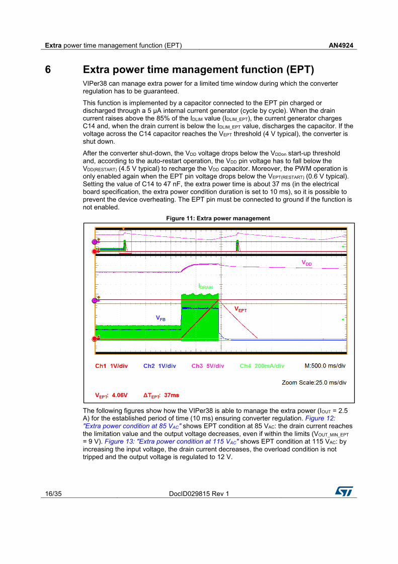
6 Extra power time management function (EPT) VIPer38 can manage extra power for a limited time window during which the converter regulation has to be guaranteed.
This function is implemented by a capacitor connected to the EPT pin charged or discharged through a 5 µA internal current generator (cycle by cycle). When the drain current raises above the 85% of the IDLIM value (IDLIM_EPT), the current generator charges C14 and, when the drain current is below the IDLIM_EPT value, discharges the capacitor. If the voltage across the C14 capacitor reaches the VEPT threshold (4 V typical), the converter is shut down.
After the converter shut-down, the VDD voltage drops below the VDDon start-up threshold and, according to the auto-restart operation, the VDD pin voltage has to fall below the VDD(RESTART) (4.5 V typical) to recharge the VDD capacitor. Moreover, the PWM operation is only enabled again when the EPT pin voltage drops below the VEPT(RESTART) (0.6 V typical). Setting the value of C14 to 47 nF, the extra power time is about 37 ms (in the electrical board specification, the extra power condition duration is set to 10 ms), so it is possible to prevent the device overheating. The EPT pin must be connected to ground if the function is not enabled.
Figure 11: Extra power management
The following figures show how the VIPer38 is able to manage the extra power (IOUT = 2.5 A) for the established period of time (10 ms) ensuring converter regulation. Figure 12: "Extra power condition at 85 VAC" shows EPT condition at 85 VAC: the drain current reaches the limitation value and the output voltage decreases, even if within the limits (VOUT_MIN_EPT = 9 V). Figure 13: "Extra power condition at 115 VAC" shows EPT condition at 115 VAC: by increasing the input voltage, the drain current decreases, the overload condition is not tripped and the output voltage is regulated to 12 V.

AN4924 Extra power time management function (EPT)
DocID029815 Rev 1 17/35
Figure 12: Extra power condition at 85 VAC
Figure 13: Extra power condition at 115 VAC

Typical waveforms AN4924
18/35 DocID029815 Rev 1
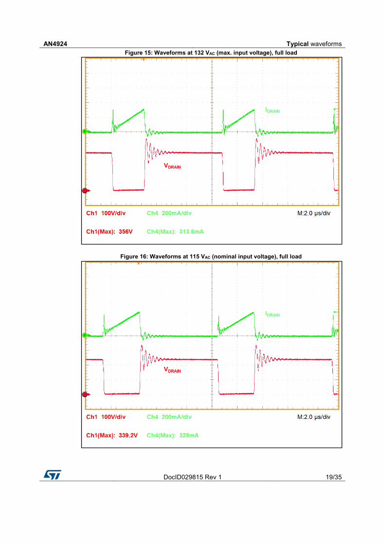
7 Typical waveforms Drain voltage and current waveforms under full load are shown in Figure 14: "Waveforms at 85 VAC (min. input voltage), full load", in Figure 15: "Waveforms at 132 VAC (max. input voltage), full load" and in Figure 16: "Waveforms at 115 VAC (nominal input voltage), full load".
Figure 14: Waveforms at 85 VAC (min. input voltage), full load
AN4924 Typical waveforms
DocID029815 Rev 1 19/35
Figure 15: Waveforms at 132 VAC (max. input voltage), full load
Figure 16: Waveforms at 115 VAC (nominal input voltage), full load

Typical waveforms AN4924
20/35 DocID029815 Rev 1
The switching frequency output ripple has also been measured. The board has an LC filter, to further reduce the ripple without reducing the ESR capacitor overall output.
The voltage ripple across the output connector (VOUT) and before the LC filter (VOUT_PRE), has been measured to verify the LC filter effectiveness.
The following figures show voltage ripple at 115 VAC in burst mode (Figure 17: "Output voltage ripple at 115 VAC, burst condition") and under full load (Figure 18: "Output voltage ripple at 115 VAC, full load").
Figure 17: Output voltage ripple at 115 VAC, burst condition

AN4924 Typical waveforms
DocID029815 Rev 1 21/35
Figure 18: Output voltage ripple at 115 VAC, full load

Typical waveforms AN4924
22/35 DocID029815 Rev 1
7.1 Dynamic step load regulation In any power supply, it is important to measure the output voltage when the converter is subjected to dynamic load variations, in order to ensure stability and prevent overvoltage or undervoltage occurrences.
For the nominal input voltage, the test was performed by varying the output load from 0 to 0.7 A (100% of nominal value) and from 0 to 2.5 A (output current under extra power condition).
In any test condition, no abnormal oscillations were noticed in the output and over/under shoot were well within acceptable values.
Figure 19: Dynamic step load at 115 VAC (IOUT from 0 to 0.7 A)

AN4924 Typical waveforms
DocID029815 Rev 1 23/35
Figure 20: Dynamic step load at 115 VAC (IOUT from 0 to 2.5 A)

Soft start AN4924
24/35 DocID029815 Rev 1
8 Soft start When the converter starts, the output capacitor is discharged and needs some time to reach the steady state condition. During this time, the control loop power demand is at the maximum, whereas the reflected voltage is low. These conditions could lead to the converter deep continuous working mode.
Furthermore, when the MOSFET is switched on, it cannot be immediately switched off as the minimum on time (TON_MIN) has to have elapsed. Because of the converter deep continuous working mode, during TON_MIN, a drain current excess can overstress the converter component, the device itself, the output diode and the transformer. Transformer saturation can also occur.
To avoid all these negative effects, the VIPer38 implements an internal soft-start feature. As the device starts working, no matter the control loop request, the drain current is allowed to gradually increase from zero to the maximum value.
The drain current limit is increased by steps and the values range from 0 to the fixed drain current limitation value (that can be regulated through an external resistor) over 16 steps. Each step length is 64 switching cycles. The soft-start phase total duration is about 8.5 ms.
The following figure shows the converter soft-start phase when operating at minimum line voltage and under maximum load.
Figure 21: Soft start

AN4924 Protection features
DocID029815 Rev 1 25/35
9 Protection features
9.1 Overload and short-circuit protection When the load power demand increases, the feedback loop increases the pin voltage. Thus, the PWM current set point increases and the power delivered to the output rises. This process ends when the delivered power equals the load power request.
In case of overload or output short-circuit (see Figure 22: "Overload: OLP triggering"), the voltage on FB pin reaches the VFBlin value (3.5 V typical) and the drain current is limited to IDlim (or the one set by the user through the RLIM resistor) by the OCP comparator. In these conditions, an internal current generator is activated and it charges the C8 capacitor; when the FB pin voltage reaches the VFBolp threshold (4.8 V typical), the converter is turned off and is not allowed to switch again until the VDD voltage falls below the VDD_RESTART(4.5 V typical) and then rises to VDDon (14 V typical).
An overload condition can be obtained by shorting the output connector. After the VDD voltage reaches the VDDon value, if the short-circuit is not removed, the system starts working in auto-restart mode (see Figure 23: "Overload: continuous"): the MOSFET switches for a short period of time and the converter tries to deliver as much power as it can to the output. Afterwards, the device does not switch and no power is processed.
As the power delivery duty cycle is very low, the average power throughput is also very low, resulting in very safe operation.
Figure 22: Overload: OLP triggering

Protection features AN4924
26/35 DocID029815 Rev 1
Figure 23: Overload: continuous
9.2 Overvoltage protection An output overvoltage protection is implemented which monitors the voltage across the auxiliary winding during the MOSFET turn off time, through the D3 diode and the R3 and R4 resistor dividers connected to the CONT pin. If this voltage exceeds the VOVP (3 V typical) threshold, an overvoltage event is assumed and an internal counter is activated; if this event occurs four consecutive times, the controller recognizes an overvoltage condition and the device stops switching. This counter provides high noise immunity and avoids spikes erroneously tripping the protection. The counter is reset every time the OVP signal is not triggered in an oscillator cycle.
After the device stops switching, to re-enable operation mode, the VDD voltage must be recycled.
The protection can be tested by opening the resistor connected to the output voltage (R10). Thus, the converter operates in open loop and the power excess with respect to the load, charges the output capacitance increasing the output voltage until the OVP is tripped and the converter stops switching.
The following figures show how the output voltage increases, and consequently, the CONT pin voltage increases; as it reaches about 3 V, the converter stops switching (at the same time the output voltage reaches about 17 V).

AN4924 Protection features
DocID029815 Rev 1 27/35
Figure 24: Overvoltage event
Figure 25: Overvoltage magnification

Protection features AN4924
28/35 DocID029815 Rev 1
9.3 2nd level overcurrent protection The VIPer38 is protected against the secondary rectifier or winding short-circuit and also against the flyback transformer saturation. Such an anomalous condition is invoked when the drain current exceeds the threshold IDMAX (1.7 A typical).
To distinguish a real malfunction from a disturbance, a warning state is entered after the first signal trip. If during the subsequent switching cycle the signal is not tripped, a temporary disturbance is assumed and the protection logic is reset; otherwise, if the IDMAX threshold is exceeded for two consecutive switching cycles, a real malfunction is assumed and the power MOSFET is turned off.
The shutdown condition is latched as long as the device is supplied. While it is disabled, no energy is transferred from the auxiliary winding; hence the VDD capacitor decays until the VDD undervoltage threshold (VDDoff), clearing the latch. VDD voltage recycles and if the fault condition is not removed the device enters the auto-restart mode.
Figure 26: 2nd level overcurrent event

AN4924 Protection features
DocID029815 Rev 1 29/35
Figure 27: 2nd level overcurrent event magnification

Conducted noise measurements AN4924
30/35 DocID029815 Rev 1
10 Conducted noise measurements The VIPer38HD frequency jittering feature allows the spectrum to spread over frequency bands, rather than being concentrated on a single frequency value. Especially when measuring conducted emission with the average detection method, the level reduction can be several dBµV.
A pre-compliance test for the EN55022 (Class B) European normative was performed and the conducted noise emission average measurements at full load and nominal input voltage is shown in Figure 28: "CE average measurements at 115 VAC, full load". There is a good margin for the measurements with respect to the limits.
Figure 28: CE average measurements at 115 VAC, full load

AN4924 Thermal measurements
DocID029815 Rev 1 31/35
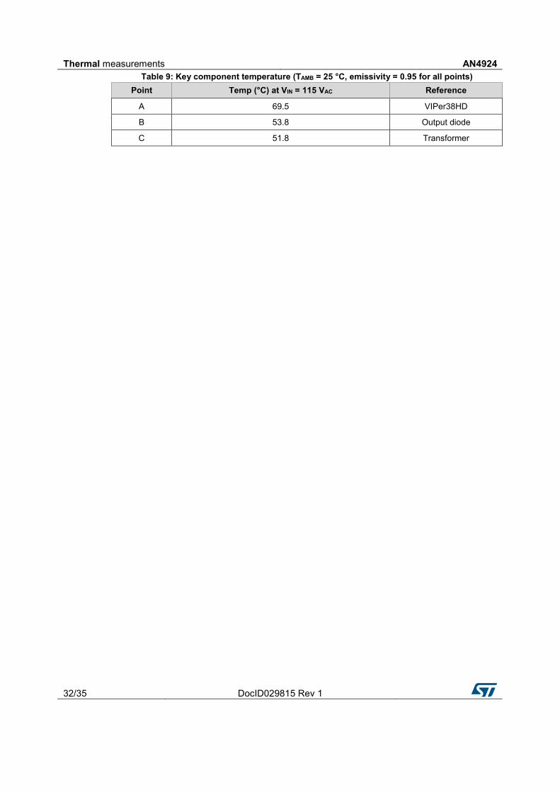
11 Thermal measurements Thermal analysis of the board was performed using an IR camera at the nominal input voltage (115 VAC), full load condition. The results are shown in the following figures and summarized in the table below.
Figure 29: Thermal measurements at 115 VAC, full load, top layer
Figure 30: Thermal measurements at 115 VAC, full load, bottom layer
Thermal measurements AN4924
32/35 DocID029815 Rev 1
Table 9: Key component temperature (TAMB = 25 °C, emissivity = 0.95 for all points) Point Temp (°C) at VIN = 115 VAC Reference
A 69.5 VIPer38HD
B 53.8 Output diode
C 51.8 Transformer

AN4924 Conclusions
DocID029815 Rev 1 33/35
12 Conclusions A flyback has been described and characterized. Special attention was paid to efficiency and low load performances and the bench results were good with very low input power under light load condition.
The efficiency performance has been compared with the EC CoC and DoE regulation program requirements for external AC/DC adapters with very good results: the measured active mode efficiency always remained above the required minimum.
The EMI emissions were also quite low, even when using a low cost input filter.

Revision history AN4924
34/35 DocID029815 Rev 1
13 Revision history Table 10: Document revision history
Date Version Changes
21-Oct-2016 1 Initial release

AN4924
DocID029815 Rev 1 35/35
IMPORTANT NOTICE – PLEASE READ CAREFULLY
STMicroelectronics NV and its subsidiaries (“ST”) reserve the right to make changes, corrections, enhancements, modifications, and improvements to ST products and/or to this document at any time without notice. Purchasers should obtain the latest relevant information on ST products before placing orders. ST products are sold pursuant to ST’s terms and conditions of sale in place at the time of order acknowledgement.
Purchasers are solely responsible for the choice, selection, and use of ST products and ST assumes no liability for application assistance or the design of Purchasers’ products.
No license, express or implied, to any intellectual property right is granted by ST herein.
Resale of ST products with provisions different from the information set forth herein shall void any warranty granted by ST for such product.
ST and the ST logo are trademarks of ST. All other product or service names are the property of their respective owners.
Information in this document supersedes and replaces information previously supplied in any prior versions of this document.
© 2016 STMicroelectronics – All rights reserved