an5032, reference circuit design for a sar adc in soc...
TRANSCRIPT
1 IntroductionA typical Analog-to-Digital Converter (ADC) compares aninput voltage with a reference voltage and generates a digitalcode corresponding to the input voltage level. Equation 1 onpage 1 gives the relation between ADC outputs and inputand reference voltage for an ideal SAR ADC. Any kind ofdisturbance at the reference will have direct impact on theoutput code. Start-up time, noise, and drive capability aresome important characteristics of any reference circuit. Thisapplication note discusses each of these characteristics indetail and provides guidelines to achieve the best possibleperformance from a Successive Approximation Register(SAR) ADC. These recommendations are supported by theoryand silicon test data that is collected at Freescale on a benchvalidation board for the MPC57XX device family. Eventhough silicon results are shared for a 12-bit, 5 V referencevoltage SAR ADC only, the guidelines are applicable for anyother SAR ADC evaluation. It is strongly recommended tovalidate the performance in addition to adhering to theguidelines in this note.
Equation 1
VIN= Analog input voltage
VREF= ADC reference voltage
Freescale Semiconductor Document Number: AN5032
Application Note Rev 0, 03/2015
Reference Circuit Design for aSAR ADC in SoCby: Siva M and Abhijan Chakravarty
© 2015 Freescale Semiconductor, Inc.
Contents
1 Introduction................................................................1
2 Characteristics of reference circuit and theirimpact on ADC performance ...................... ............. 2
2.1 Start-up time................................................... 2
2.2 Drive capability.............................................. 4
2.3 Noise...............................................................5
3 Step-by-step procedure to design areference circuit......................................................... 9
4 Summary............................... .................................. 11
5 References.............................. ................................. 11

N= Resolution of ADC
Figure 1. Typical ADC reference circuit
2 Characteristics of reference circuit and their impact onADC performance
2.1 Start-up time
The time required for the output voltage to reach its final value within a specified error band is defined as start-up time orturn-on time. Start-up time of a voltage reference circuit is a function of output load capacitance and voltage level. Mostmicrocontroller applications may not require continuous operation. There are applications where the ADC circuit will beturned off and will be switched on when required. The on-time of a typical microcontroller while booting from flash will bein the order of 5 ms. The reference voltage circuits should start-up faster than the ADC to provide a stable reference voltagefor the ADC to operate. Figure 2 and Figure 3 show the Start-up time profile of slow and fast reference circuits. Figure 4 andFigure 5 show the corresponding ADC output code profile for a DC input. This shows that before the ADC starts conversion,the reference voltage must be stable to get the correct output code.
Characteristics of reference circuit and their impact on ADC performance
Reference Circuit Design for a SAR ADC in SoC, Rev 0, 03/2015
2 Freescale Semiconductor, Inc.

Figure 2. Start-up time profile of slow reference circuit
Figure 3. Start-up time profile of fast reference circuit
Characteristics of reference circuit and their impact on ADC performance
Reference Circuit Design for a SAR ADC in SoC, Rev 0, 03/2015
Freescale Semiconductor, Inc. 3

Figure 4. ADC output using slow start-up time reference circuit
Figure 5. ADC output using fast start-up time reference circuit
2.2 Drive capability
Selection of a reference source depends on the application. Figure 1 shows a typical reference circuit driving a standaloneADC. It consists of a voltage reference source and decoupling capacitors. A voltage reference circuit will have good start-uptime but low drive capability in the order of 10 mA to 20 mA. This is sufficient to drive a standalone ADC. However, in anSoC environment, multiple ADC instances may be present. Most of the time, these will share a common reference. In somecases, the supply voltage input and the reference voltage input may even be shorted. Here, an op-amp based buffer circuit canbe added between voltage reference and reference pin to meet the load conditions as shown in Figure 6. The voltagereference source and buffer can be replaced with a single linear voltage regulator (LDO). In today's market, a wide range ofLDOs are available which have very low noise and fast startup times. Also, some LDOs support an adjustable output voltagewhich eliminates the need for an additional buffer circuit. Figure 7 shows a Low-dropout (LDO) voltage regulator driving anADC reference pin. Here, Ro is the equivalent series resistance (sum of output resistance of LDO, trace resistance) betweenthe voltage regulator and the ADC reference pin. This resistance should be low enough such that the voltage drop will be lessthan 0.5 LSB from the LDO output pin to the ADC reference pin to avoid any conversion errors.
Characteristics of reference circuit and their impact on ADC performance
Reference Circuit Design for a SAR ADC in SoC, Rev 0, 03/2015
4 Freescale Semiconductor, Inc.

Figure 6. Voltage reference and buffer driving ADCs in SoC
Figure 7. Linear voltage regulator driving ADCs in SoC
2.3 Noise
Common sources of noise are listed below:• Ground bounce due to resistance and inductance in the reference path: Resistance and Inductance in the reference
path can be minimized by connecting decoupling capacitors as close as possible to the supply pins and ground planes.The effect of ground bounce in the reference path can be clearly observed when high inductance contactors are used fortesting SAR ADCs [2 ].
• Interaction of analog and digital switching currents: A common ground plane is recommended for a typical dataconverter system. The designer should make sure the analog and digital ground return currents are localized by creatingshort routes. A well-designed board should have the analog and digital circuits in separate sections of the board (withminimum overlapping).
• Reference source (LDO noise): The reference circuit noise should be at least 10 dB better than the Device Under Test(DUT) [1 ].
To verify the effect of reference noise two types of reference circuits are selected.• 50 μV rms noise integrated noise from DC to 100 kHz- will be referred as low noise reference source• 500 μV rms noise integrated noise from DC to 100 kHz- will be referred as high noise reference source
Figure 8 and Figure 9 show the linearity data collected using a low noise and a high noise reference circuit at the samecondition. A Differential Non-Linearity (DNL) flare up at higher codes can be observed with the noisy reference circuit.Figure 10 and Figure 11 show FFT plots collected using low noise and noisy source reference circuits. Figure 12 shows the
Characteristics of reference circuit and their impact on ADC performance
Reference Circuit Design for a SAR ADC in SoC, Rev 0, 03/2015
Freescale Semiconductor, Inc. 5

low frequency noise profile with zoom for a low noise and noisy source reference circuit. Low frequency noise can be relatedto the reference circuit noise profile. Given the importance of the quality of the reference source, it is important to pick agood quality source to drive the SAR ADC reference.
If the reference noise level is close to the ADC noise level, a trend may not be visible in static (e.g. DNL) and dynamic (e.g.Signal-to-Noise Ratio (SNR)) plots. However, the ADC can show degradation in the performance numbers. To confirmwhether the performance degradation is due to reference noise or not, a simple experiment can be done.
Collect system noise at several values of analog input voltages from 0 to full scale. In this experiment, the input should berelatively low noise as compared to ADC noise. Figure 13 shows the variation of system noise with input voltage for a typicalSAR ADC. Here, data is collected with low noise reference and a noisy voltage reference source at the same conditions.Figure 13 clearly shows if the reference circuit noise is relatively low as compared to ADC noise, then the overall systemnoise (reference noise + ADC noise) is constant, otherwise, it will linearly increase with ADC input [3 ]. This experiment canbe used to find if any reference noise trend exists even in the order of LSBs.
Figure 8. DNL and INL using low noise reference source
Characteristics of reference circuit and their impact on ADC performance
Reference Circuit Design for a SAR ADC in SoC, Rev 0, 03/2015
6 Freescale Semiconductor, Inc.
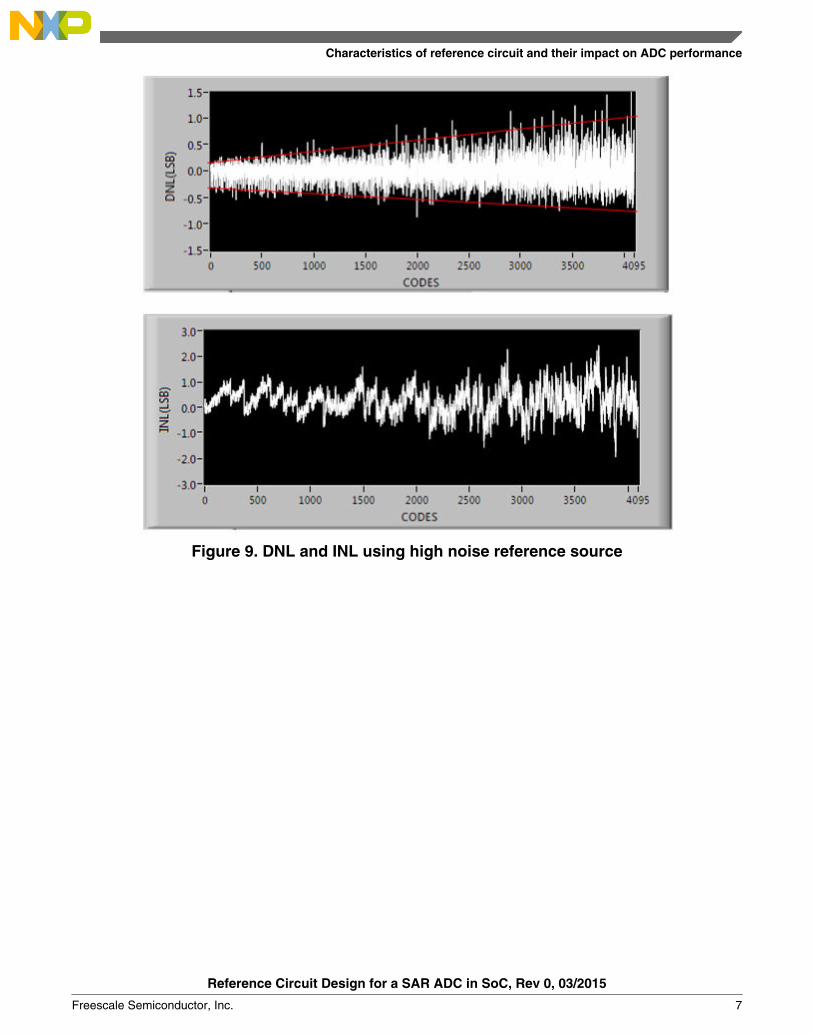
Figure 9. DNL and INL using high noise reference source
Characteristics of reference circuit and their impact on ADC performance
Reference Circuit Design for a SAR ADC in SoC, Rev 0, 03/2015
Freescale Semiconductor, Inc. 7

Figure 10. SAR ADC FFT using low noise reference source
Figure 11. SAR ADC FFT using high noise reference source
Characteristics of reference circuit and their impact on ADC performance
Reference Circuit Design for a SAR ADC in SoC, Rev 0, 03/2015
8 Freescale Semiconductor, Inc.

Figure 12. SAR ADC FFT with highlighted low frequency noise
Figure 13. Effect of reference noise on the ADC performance
3 Step-by-step procedure to design a reference circuitIn the previous sections, effect of Start-up time, Noise and importance of Drive capability is discussed. This section providesa step-by-step procedure for designing a SAR ADC reference circuit. Design steps are given for below specifications of aSAR ADC.
Reference voltage, VREF=5.0 V
Average reference current, IREF=100 µA
Resolution, N=12-bit
Step 1: Calculation of maximum allowed series resistance in the reference path:
Step-by-step procedure to design a reference circuit
Reference Circuit Design for a SAR ADC in SoC, Rev 0, 03/2015
Freescale Semiconductor, Inc. 9

Equation 2
Equation 3
Equation 4
Equation 5
Ensure resistance between the reference circuit and the ADC reference pin (sum of LDO output resistance, PCB traceresistance) is less than the above calculated value.
Step 2: Calculation of minimum required decoupling capacitor in the reference path:
For good stability, a regulator datasheet typically recommends a minimum capacitor value at the voltage output pin.Similarly, for SAR ADC, the device documentation contains a recommendation on the minimum value of decouplingcapacitors to be used. In such a case, pick the higher of these two so that it meets the requirements of both circuits.
Step 3: Calculation of maximum allowed noise in the reference path:
The reference circuit with decoupling capacitor will form a first order low pass filter. Its noise bandwidth (BW) is given by:
Equation 6
Equation 7
where,
R0=Total resistance between regulator and reference pin of ADC.
Ceq=Total capacitance connected at the ref pin.
Procedure to calculate Ro & Ceq is provided in step 1 & 2.
Let’s assume these values are as follows:
R0=0.5 Ω
Ceq=4.7 µF + 0.1 µF (bulk & small capacitor)
The noise bandwidth would then be
Equation 8
Generally, LDO datasheets provide noise profile details. One must make sure that the reference circuit noise integrated overthe noise BW (as per Equation 7 on page 10) is 10 dB better than the DUT [1 ].
Step-by-step procedure to design a reference circuit
Reference Circuit Design for a SAR ADC in SoC, Rev 0, 03/2015
10 Freescale Semiconductor, Inc.

4 SummaryStartup time, stability, drive capability, and noise are some of the important characteristics which need to be considered whileselecting a reference source for a SAR ADC. To get the best dynamic performance, the reference system noise profile shouldbe at least 10 dB better than DUT. The SAR ADC presents a dynamic load, therefore the reference circuit should have gooddriving capability. With advancement in VLSI technology, low noise and startup time LDOs available in the market providea good fit for driving multiple high resolution SAR ADCs.
5 References1. AN4881: MPC57xx SAR ADC Implementation and Use, available at freescale.com .2. Maugard, G., C. Wegneer, T. O’Dwye, M.P. Kennedy. "Method of reducing contactor effect when testing high-
precision ADCs," Test Conference, 2003, Proceedings, ITC 2003.3. Oljaca, M., W. Klein. "Converter voltage reference performance improvement secrets," Instrumentation &
Measurement Magazine, IEEE, Volume: 12, Issue: 5 October 2009.
Summary
Reference Circuit Design for a SAR ADC in SoC, Rev 0, 03/2015
Freescale Semiconductor, Inc. 11

How to Reach Us:
Home Page:freescale.com
Web Support:freescale.com/support
Information in this document is provided solely to enable system andsoftware implementers to use Freescale products. There are no expressor implied copyright licenses granted hereunder to design or fabricateany integrated circuits based on the information in this document.Freescale reserves the right to make changes without further notice toany products herein.
Freescale makes no warranty, representation, or guarantee regardingthe suitability of its products for any particular purpose, nor doesFreescale assume any liability arising out of the application or use ofany product or circuit, and specifically disclaims any and all liability,including without limitation consequential or incidental damages.“Typical” parameters that may be provided in Freescale data sheetsand/or specifications can and do vary in different applications, andactual performance may vary over time. All operating parameters,including “typicals,” must be validated for each customer application bycustomer's technical experts. Freescale does not convey any licenseunder its patent rights nor the rights of others. Freescale sells productspursuant to standard terms and conditions of sale, which can be foundat the following address: freescale.com/SalesTermsandConditions.
Freescale and the Freescale logo are trademarks of FreescaleSemiconductor, Inc., SafeAssure and SafeAssure logo are trademarksof Freescale Semiconductor, Inc.Reg. U.S. Pat. & Tm. Off. All otherproduct or service names are the property of their respective owners.
© 2015 Freescale Semiconductor, Inc.
Document Number AN5032Revision 0, 03/2015