ana add1000b datasheet - futureelectronics.com semiconductor/add1000bsk.pdf · add1000b datasheet...
TRANSCRIPT
ADD1000B Datasheet Doc Rev 1.05 Datasheet — 11-Aug-2010
Document information
Info Content
Author J.G.
Keywords 1000B, Datasheet
Abstract

ADD Semiconductor
ADD1000B Datasheet
Preliminary
©Advanced Digital Design. 2010. All rights reserved.
Doc Rev 1.05 Datasheet — 11-Aug-2010 2
Revision History
Revision Date Description Author
1.03 2010-03-29 Second revision J.G.
1.04 2010-05-25 Max output current values updated J.G.
1.05 2010-08-11 Annex2 updated A.M.A.
Copyright: © 2010 ADD Semiconductor. All rights reserved.
ADD Semiconductor does not warrant nor represent that any license, either expressed or implied is granted under any ADD Semiconductor patent right, copyright, mask work right or other ADD Semiconductor intellectual property right relating to any combination, machine or process in which ADD Semiconductor product and services are used. Information published by ADD Semiconductor regarding third party products or services does not constitute a license from ADD Semiconductor to use such products or services or a warranty of endorsement thereof. Use of such information may require a license from a third party under the patents or other intellectual property of the third party or a license from ADD Semiconductor under the patents or other intellectual property of ADD Semiconductor. Third party trademarks are hereby acknowledged.
Liability disclaimer
ADD Semiconductor reserves the right to make changes without further notice to the product to improve reliability, functionality or design. ADD Semiconductor does not assume any liability arising out of the application or use of any product or circuits described herein. All application information is advisory and does not form part of the specification.
Life support applications
These products are not designed for its use in life support appliances, devices or systems where malfunction of these products can reasonably be expected to result in personal injury. ADD Semiconductor customers using or selling these products for use in such applications do so at their own risk and agree to fully indemnify ADD Semiconductor for any damages resulting from such improper use or sale.
Contact details
For your nearest distributor, please see www.addsemi.com
Receive available updates automatically by subscribing to eNews from our homepage or check our website regularly for any available updates.
Headquarters: Torre C2, Pol. Puerta Norte, A-23 Km. 509, 50820 Zaragoza (Spain)
Phone: +34 976 526 761; Fax: +34 976 361 994
www.addsemi.com

ADD Semiconductor
ADD1000B Datasheet
Preliminary
©Advanced Digital Design. 2010. All rights reserved.
Doc Rev 1.05 Datasheet — 11‐Aug‐2010 3
Contents1. General Description .................................... 4 1.1 Block Diagram ............................................. 5 1.2 Pin Assignment ........................................... 6 2. Electrical Characteristics ......................... 11 2.1 Absolute Maximum Ratings ..................... 11 2.2 Recommended Operating Conditions .... 12 2.3 DC Characteristics .................................... 13 2.4 Power Consumption ................................. 14 2.5 Thermal data .............................................. 14 2.6 Oscillator .................................................... 15 2.7 Power-on .................................................... 17 3. Mechanical data ......................................... 18 3.1 Recommended mounting conditions ...... 19 3.1.1 Conditions of Standard Reflow ........... 19 Temperature Profile ............................................... 19 3.1.2 Manual Soldering .................................. 20 4. Annex 1 ....................................................... 21 5. Annex 2 ....................................................... 23 5.1 ADD1000B Application circuit example . 24 5.2 Analog Front End example ...................... 25
ADD Semiconductor ADD1000B Datasheet
©Advanced Digital Design. 2010. All rights reserved.
Doc Rev 1.05 Datasheet — 11‐Aug‐2010 4
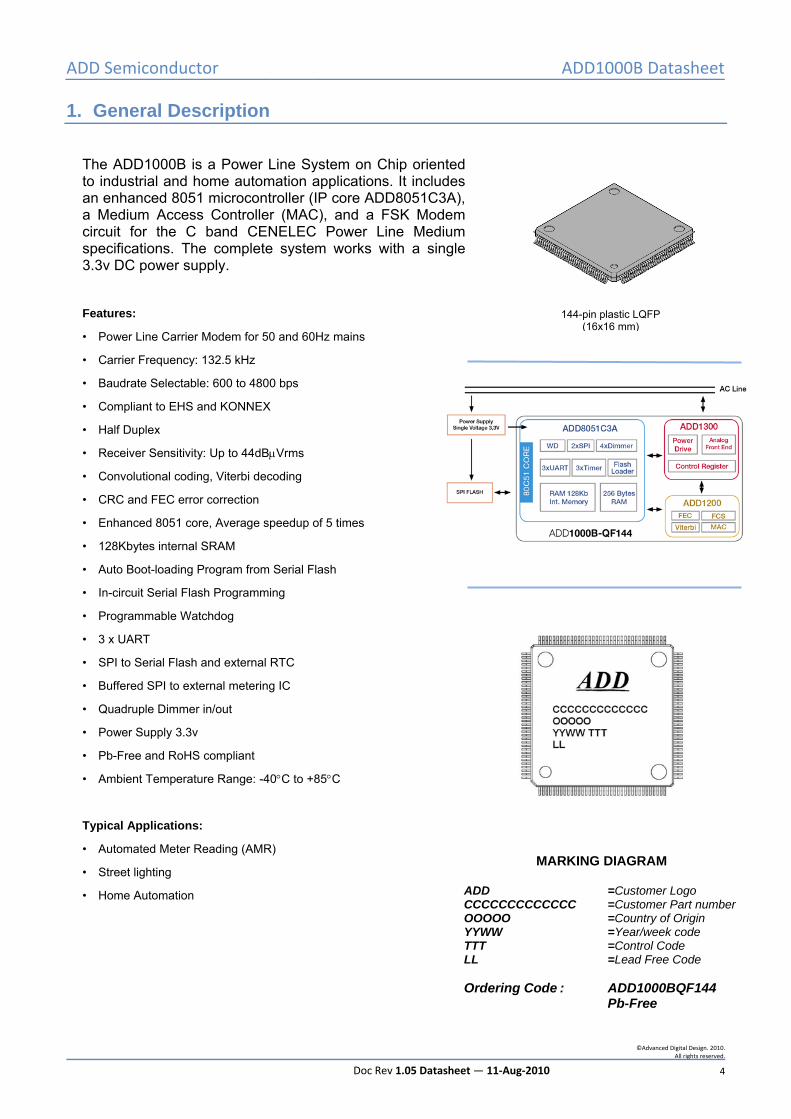
1. General Description
The ADD1000B is a Power Line System on Chip oriented to industrial and home automation applications. It includes an enhanced 8051 microcontroller (IP core ADD8051C3A), a Medium Access Controller (MAC), and a FSK Modem circuit for the C band CENELEC Power Line Medium specifications. The complete system works with a single 3.3v DC power supply. Features:
• Power Line Carrier Modem for 50 and 60Hz mains
• Carrier Frequency: 132.5 kHz
• Baudrate Selectable: 600 to 4800 bps
• Compliant to EHS and KONNEX
• Half Duplex
• Receiver Sensitivity: Up to 44dBμVrms
• Convolutional coding, Viterbi decoding
• CRC and FEC error correction
• Enhanced 8051 core, Average speedup of 5 times
• 128Kbytes internal SRAM
• Auto Boot-loading Program from Serial Flash
• In-circuit Serial Flash Programming
• Programmable Watchdog
• 3 x UART
• SPI to Serial Flash and external RTC
• Buffered SPI to external metering IC
• Quadruple Dimmer in/out
• Power Supply 3.3v
• Pb-Free and RoHS compliant
• Ambient Temperature Range: -40°C to +85°C
Typical Applications:
• Automated Meter Reading (AMR)
• Street lighting
• Home Automation
MARKING DIAGRAM
ADD =Customer Logo CCCCCCCCCCCCC =Customer Part number OOOOO =Country of Origin YYWW =Year/week code TTT =Control Code LL =Lead Free Code Ordering Code : ADD1000BQF144 Pb-Free
144-pin plastic LQFP (16x16 mm)
ADD Semiconductor ADD1000B Datasheet
©Advanced Digital Design. 2010. All rights reserved.
Doc Rev 1.05 Datasheet — 11‐Aug‐2010 5
1.1 Block Diagram
JTAG Bscan
DEBUGRESET
Clock
ResetInterface
ClockInterface
PowerManagement
CODESRAM
BOOTLOADER
SPI0
XDATASRAM
SPI1
UART0
UART1
UART2
TIMER0
TIMER1
TIMER2
T11, T12, T14
WATCHDOG
GENERALPURPOSE I/O
DIMMERPERIPHERAL
MEDIUMACCESSCONTROL
Vref1Vref2
EMIT(12:1)
ENABLEDC_COMP
D_IND_NIN
REC(8:1)VINVRHVRL
8051C3A Core
PLCMODEM
MUX
IDATA
128KB SRAM
TRIAC_(3:0)
VNR
D_INIT RSTA
CLKA
CLKB
P5(3:0)
P4(5:2)
P3(1:0)
P5(5:4)
P4(1:0)
P3.4/T0
P3.5/T1
P4.6/T2
P4.7/T2EX
VDD
VSS
LDO_PD
VDEO
INTA(3:0)
INTB(3:0)
INTC(3:0)
INTD(3:0)
AVD AVS
TDITDOTCK
TMSTRST
/EWDG
DEBUG
/PROG
SECURED
P1.7/ SSN
11.059.200Hz
INT1
EMIT0
Figure 1. ADD1000B Block Diagram

ADD Semiconductor ADD1000B Datasheet
©Advanced Digital Design. 2010. All rights reserved.
Doc Rev 1.05 Datasheet — 11‐Aug‐2010 6
1.2 Pin Assignment
The following figure illustrates the pinout of the ADD1000B LQFP144 package:
P3_3/INT1VccGndGndGndTDI
TDOTCKTMS
TRSTD_INITRSTA
/PROGSECURED
/EWDGDEBUG
VccCLKEB
GndCLKEA
VccGndGndVDEO
VDEO
VSSO
LDO_PDVDD
GndVcc
Vref1Vref2VNR
TRIAC_3TRIAC_2TRIAC_1
TRIA
C_0
P5_
5/TX
D1/
INTA
1P5
_4/R
XD1/
INTA
0P4
_7/T
2EX
/INTA
3P4
_6/T
2/IN
TA2
P1_
7/SS
NVc
cG
ndEM
IT_0
EMIT
_1EM
IT_2 Vc
cG
ndEM
IT_3
EMIT
_4EM
IT_5
EMIT
_6 Vcc
Gnd
EMIT
_7EM
IT_8
EMIT
_9EM
IT_1
0Vc
cG
ndEM
IT_1
1EM
IT_1
2Vc
cG
ndP3
_1/T
XD0
P3_0
/RXD
0P4
_5/M
ISO
1/IN
TB3
P4_4
/MO
SI1/
INTB
2P4
_3/S
PIC
LK1/
INTB
1P
4_2/
SS1/
INTB
0P4
_1/T
XD2
INTD0INTD1INTD2INTD3GndVccNCNCNCNCNCNCNCNCNCNCNCGndVccVDD
NCNCNCNCNCNCNCNCNCINTC0INTC1INTC2INTC3GndVccP4_0/RXD2
P3_4
/T0
P3_5
/T1
P5_0
/SS0
P5_1
/SPI
CLK
0P5
_2/M
OS
I0P5
_3/M
ISO
0G
ndVc
cA V
S2
A VD
2
A VS
1
A VD
1
VRH
VIN
VRL
Gnd
Vcc
REC
_8R
EC_7
REC
_6R
EC_5
REC
_4R
EC_3
REC
_2R
EC_1
DIN
DN
ING
ndEN
ABLE
Vcc
DC
_CO
MP
Gnd
NC
NC
NC
NC
123456789101112131415161718192021222324252627282930313233343536
37 38 39 40 41 42 43 44 45 46 47 48 49 50 51 52 53 54 55 56 57 58 59 60 61 62 63 64 65 66 67 68 69 70 71 72
108107106105104103102101100999897969594939291908988878685848382818079787776757473
144
143
142
141
140
139
138
137
136
135
134
133
132
131
130
129
128
127
126
125
124
123
122
121
120
119
118
117
116
115
114
113
112
111
110
109
Figure 2. LQFP pin assignment

ADD Semiconductor ADD1000B Datasheet
©Advanced Digital Design. 2010. All rights reserved.
Doc Rev 1.05 Datasheet — 11‐Aug‐2010 7
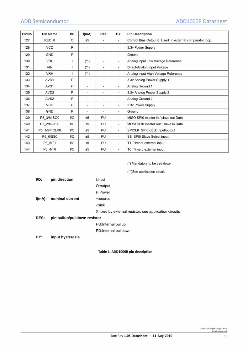
PinNo Pin Name I/O I(mA) Res HY Pin Description
1 P3_3/INT1 I/O ±5 PU - INT1 external interrupt 1
2 VCC P - - - 3.3v Power Supply
3 GND P - - - Ground
4 GND P - - - Ground (*)
5 GND P - - - Ground (*)
6 TDI I ±5 PU - JTAG Test Data In
7 TDO O ±5 - - JTAG Test Data Out
8 TCK I ±5 - - JTAG Test Clock
9 TMS I ±5 PU - JTAG Test Mode Select
10 TRST I ±5 PU - JTAG Test Reset
11 D_INIT I ±5 PD Y Initialization signal
12 RSTA I ±5 PD Y Asynchronous Reset
13 /PROG I ±5 PU Y SPI Flash programming pin
14 SECURED I ±5 PD Y Encryption enabling
15 /EWDG I ±5 PD Y Watchdog enable. Active low
16 DEBUG I ±5 PD Y Debug mode enable
17 VCC P - - - 3.3v Power Supply
18 CLKEB I/O - - - External clock reference. The user may connect CLKEB to a compatible oscillator or to one terminal of a crystal oscillator
19 GND P - - - Ground
20 CLKEA I - - - External clock reference. The user may connect CLKEA to the other terminal of the crystal oscillator or tie CLKEA to ground
21 VCC P - - - 3.3v Power Supply
22 GND P - - - Ground
23 GND P - - - Ground
24 VDE0 P - - - LDO power input.
25 VDE0 P - - - LDO power input.
26 VSS0 P - - - LDO ground
27 LDO_PD I LDO Power down
28 VDD P - - - LDO power output. A capacitor in the range 0.1μF-10μF must be connected here
29 GND P - - - Ground
30 VCC P - - - 3.3v Power Supply
31 Vref1 I - - - Voltage reference 1. Tie to Vcc with a Rpu=4k7Ω
32 Vref2 I - - - Voltage reference 2. Tie to Ground with a Rpd=4k7Ω
33 VNR I ±5 - Y Zero Crossing Detection signal. Used in Home Automation control pins
34 TRIAC_3 O ±5 - - Home Automation Control 3
35 TRIAC_2 O ±5 - - Home Automation Control 2
36 TRIAC_1 O ±5 - - Home Automation Control 1
37 TRIAC_0 O ±5 - - Home Automation Control 0
38 P5_5/TXD1/INTA1 I/O ±5 PU - TxD Serial Port 1 output. Can be configured as dimmer switch input
39 P5_4/RXD1/INTA0 I/O ±5 PU - RxD Serial Port 1 input. Can be configured as dimmer switch input
40 P4_7/T2EX/INTA3 I/O ±5 PU - T2EX Timer2 External input. Can be configured as dimmer switch input
41 P4_6/T2/INTA2 I/O ±5 PU - T2 Timer2 input/output. Can be configured as dimmer switch input
ADD Semiconductor ADD1000B Datasheet
©Advanced Digital Design. 2010. All rights reserved.
Doc Rev 1.05 Datasheet — 11‐Aug‐2010 8
PinNo Pin Name I/O I(mA) Res HY Pin Description
42 P1_7/SSN I/O ±5 PU - Silicon Serial Number input. (P1.7 must not be used as generic control port since it searches for a Silicon Serial number device at start-up and could put out undesirable transient values)
43 VCC P - - - 3.3v Power Supply
44 GND P - - - Ground
45 EMIT_0 O ±X - - TXRX control output pin
46 EMIT_1 O ±X - - PLC Transmission port 1
47 EMIT_2 O ±X - - PLC Transmission port 2
48 VCC P - - - 3.3v Power Supply
49 GND P - - - Ground
50 EMIT_3 O ±X - - PLC Transmission port 3
51 EMIT_4 O ±X - - PLC Transmission port 4
52 EMIT_5 O ±X - - PLC Transmission port 5
53 EMIT_6 O ±X - - PLC Transmission port 6
54 VCC P - - - 3.3v Power Supply
55 GND P - - - Ground
56 EMIT_7 O ±X - - PLC Transmission port 7
57 EMIT_8 O ±X - - PLC Transmission port 8
58 EMIT_9 O ±X - - PLC Transmission port 9
59 EMIT_10 O ±X - - PLC Transmission port 10
60 VCC P - - - 3.3v Power Supply
61 GND P - - - Ground
62 EMIT_11 O ±X - - PLC Transmission port 11
63 EMIT_12 O ±X - - PLC Transmission port 12
64 VCC P - - - 3.3v Power Supply
65 GND P - - - Ground
66 P3_1/TXD0 I/O ±5 PU - TxD Serial Port 0 output
67 P3_0/RXD0 I/O ±5 PU - RxD Serial Port 0 input
68 P4_5/MISO1/INTB3 I/O ±5 PU - MISO1 SPI1 master in / slave out Data. Can be configured as dimmer switch input
69 P4_4/MOSI1/INTB2 I/O ±5 PU - MOSI1 SPI1 master out / slave in Data. Can be configured as dimmer switch input
70 P4_3/SPICLK1/INT
B1 I/O ±5 PU - SPICLK1 SPI1 clock input/output. Can be configured as dimmer switch input
71 P4_2/SS1/INTB0 I/O ±5 PU - SS1 SPI1 Slave Select input. Can be configured as dimmer switch input
72 P4_1/TXD2 I/O ±5 PU - TxD Serial Port 2 output
73 P4_0/RXD2 I/O ±5 PU - Rxd Serial Port 2 input
74 VCC P - - - 3.3v Power Supply
75 GND P - - - Ground
76 INTC3 I ±5 - - Can be configured as dimmer switch input or left unconnected
77 INTC2 I ±5 - - Can be configured as dimmer switch input or left unconnected
78 INTC1 I ±5 - - Can be configured as dimmer switch input or left unconnected
79 INTC0 I ±5 - - Can be configured as dimmer switch input or left unconnected
80 NC - - - - Do Not Connect
81 NC - - - - Do Not Connect
82 NC - - - - Do Not Connect
83 NC - - - - Do Not Connect

ADD Semiconductor ADD1000B Datasheet
©Advanced Digital Design. 2010. All rights reserved.
Doc Rev 1.05 Datasheet — 11‐Aug‐2010 9
PinNo Pin Name I/O I(mA) Res HY Pin Description
84 NC - - - - Do Not Connect
85 NC - - - - Do Not Connect
86 NC - - - - Do Not Connect
87 NC - - - - Do Not Connect
88 NC - - - - Do Not Connect
89 VDD P - - - LDO power output. A capacitor in the range 0.1μF-10μF must be connected here
90 VCC P - - - 3.3v Power Supply
91 GND P - - - Ground
92 NC - - - - Do Not Connect
93 NC - - - - Do Not Connect
94 NC - - - - Do Not Connect
95 NC - - - - Do Not Connect
96 NC - - - - Do Not Connect
97 NC - - - - Do Not Connect
98 NC - - - - Do Not Connect
99 NC - - - - Do Not Connect
100 NC - - - - Do Not Connect
101 NC - - - - Do Not Connect
102 NC - - - - Do Not Connect
103 VCC P - - - 3.3v Power Supply
104 GND P - - - Ground
105 INTD3 I ±5 - - Can be configured as dimmer switch input or left unconnected
106 INTD2 I ±5 - - Can be configured as dimmer switch input or left unconnected
107 INTD1 I ±5 - - Can be configured as dimmer switch input or left unconnected
108 INTD0 I ±5 - - Can be configured as dimmer switch input or left unconnected
109 NC - - - - Do Not Connect
110 NC - - - - Do Not Connect
111 NC - - - - Do Not Connect
112 NC - - - - Do Not Connect
113 GND P - - - Ground
114 DC_COMP O ±10 - - Direct Current pin, used in external comparator loop
115 VCC P - - - 3.3v Power Supply
116 ENABLE O ±10 - - External comparator latch enable signal
117 GND P - - - Ground
118 DNIN I ±5 - - External comparator negative output pin
119 DIN I ±5 - - External comparator output pin
120 REC_1 O ±5 - - Control Bias Output 1. Used in external comparator loop
121 REC_2 O ±5 - - Control Bias Output 2. Used in external comparator loop
122 REC_3 O ±5 - - Control Bias Output 3. Used in external comparator loop
123 REC_4 O ±5 - - Control Bias Output 4. Used in external comparator loop
124 REC_5 O ±5 - - Control Bias Output 5. Used in external comparator loop
125 REC_6 O ±5 - - Control Bias Output 6. Used in external comparator loop
126 REC_7 O ±5 - - Control Bias Output 7. Used in external comparator loop
ADD Semiconductor ADD1000B Datasheet
©Advanced Digital Design. 2010. All rights reserved.
Doc Rev 1.05 Datasheet — 11‐Aug‐2010 10
PinNo Pin Name I/O I(mA) Res HY Pin Description
127 REC_8 O ±5 - - Control Bias Output 8. Used in external comparator loop
128 VCC P - - - 3.3v Power Supply
129 GND P - - - Ground
130 VRL I (**) - - Analog input Low Voltage Reference
131 VIN I (**) - - Direct-Analog Input Voltage
132 VRH I (**) - - Analog input High Voltage Reference
133 AVD1 P - - - 3.3v Analog Power Supply 1
134 AVS1 P - - - Analog Ground 1
135 AVD2 P - - - 3.3v Analog Power Supply 2
136 AVS2 P - - - Analog Ground 2
137 VCC P - - - 3.3v Power Supply
138 GND P - - - Ground
139 P5_3/MISO0 I/O ±5 PU - MISO SPI0 master in / slave out Data
140 P5_2/MOSI0 I/O ±5 PU - MOSI SPI0 master out / slave in Data
141 P5_1/SPICLK0 I/O ±5 PU - SPICLK SPI0 clock input/output
142 P5_0/SS0 I/O ±5 PU - SS SPI0 Slave Select input
143 P3_5/T1 I/O ±5 PU - T1 Timer1 external input
144 P3_4/T0 I/O ±5 PU - T0 Timer0 external input
(*) Mandatory to be tied down
(**)See application circuit
I/O: pin direction I:Input
O:output
P:Power
I(mA): nominal current +:source
-:sink
X:fixed by external resistor, see application circuits
RES: pin pullup/pulldown resistor PU:Internal pullup
PD:Internal pulldown
HY: input hysteresis
Table 1. ADD1000B pin description

ADD Semiconductor ADD1000B Datasheet
©Advanced Digital Design. 2010. All rights reserved.
Doc Rev 1.05 Datasheet — 11‐Aug‐2010 11
2. Electrical Characteristics
2.1 Absolute Maximum Ratings
Permanent device damage may occur if Absolute Maximum Ratings are exceeded. Functional operation should be restricted to the conditions given in the Recommended Operating Conditions section. Exposure to the Absolute Maximum Conditions for extended periods may affect device reliability. (VSS = 0 V)
Parameter Symbol Rating Unit
Supply Voltage VCC -0.5 to 4.0 V
Input Voltage VI -0.5 to VCC+0.5(≤4.0V) V
Output Voltage VO -0.5 to VCC+0.5(<4.0V) V
Storage Temperature TST -55 to 125 ºC
Junction Temperature TJ -40 to 125 ºC
Output Current (*)1 IO ±10 (*)2 mA
Notes:
(*)1. DC current that continuously flows for 10ms or more, or average DC current.
(*)2. Applies to all the pins except EMIT pins. EMIT pins should be only used according to circuit configurations recommended by ADD.
ATTENTION Observe ESD Precautions
Precautions for handling electrostatic sensitive devices should be taken into account to avoid malfunction. Charged devices and circuit boards can discharge without detection.
ADD Semiconductor ADD1000B Datasheet
©Advanced Digital Design. 2010. All rights reserved.
Doc Rev 1.05 Datasheet — 11‐Aug‐2010 12
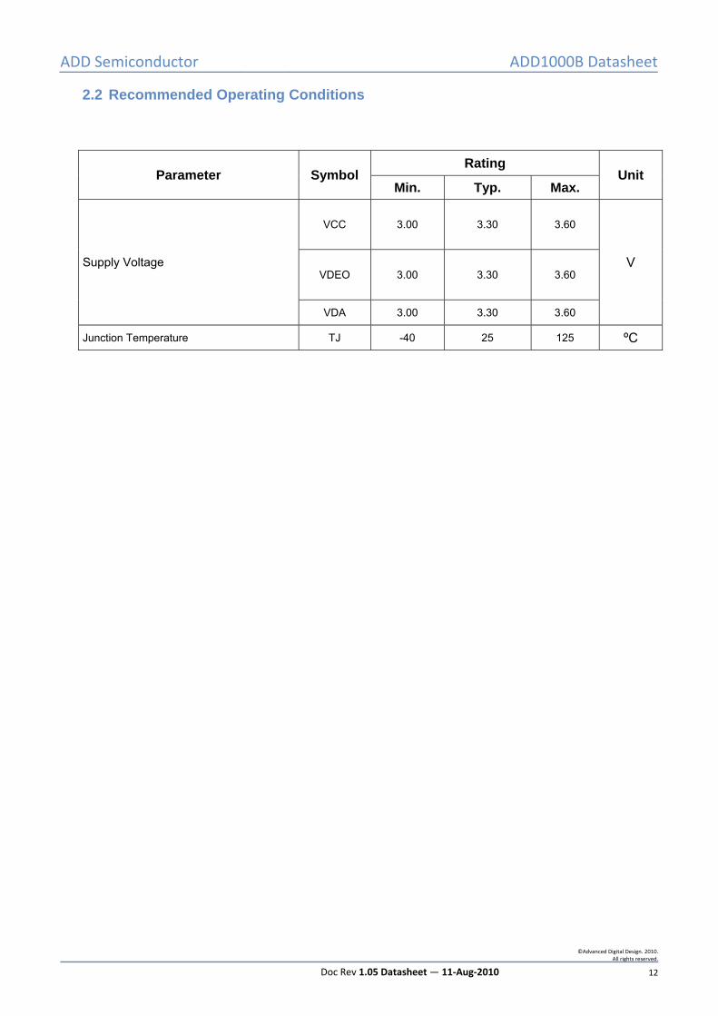
2.2 Recommended Operating Conditions
Parameter Symbol Rating
Unit Min. Typ. Max.
Supply Voltage
VCC 3.00 3.30 3.60
V VDEO 3.00 3.30 3.60
VDA 3.00 3.30 3.60
Junction Temperature TJ -40 25 125 ºC
ADD Semiconductor ADD1000B Datasheet
©Advanced Digital Design. 2010. All rights reserved.
Doc Rev 1.05 Datasheet — 11‐Aug‐2010 13
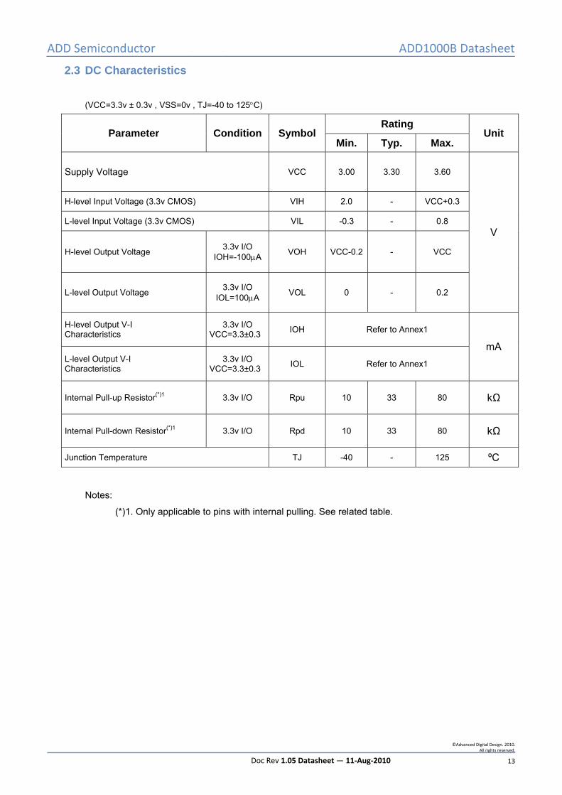
2.3 DC Characteristics
(VCC=3.3v ± 0.3v , VSS=0v , TJ=-40 to 125°C)
Parameter Condition Symbol Rating
Unit Min. Typ. Max.
Supply Voltage VCC 3.00 3.30 3.60
V
H-level Input Voltage (3.3v CMOS) VIH 2.0 - VCC+0.3
L-level Input Voltage (3.3v CMOS) VIL -0.3 - 0.8
H-level Output Voltage 3.3v I/O IOH=-100μA VOH VCC-0.2 - VCC
L-level Output Voltage 3.3v I/O IOL=100μA VOL 0 - 0.2
H-level Output V-I Characteristics
3.3v I/O VCC=3.3±0.3 IOH Refer to Annex1
mA L-level Output V-I Characteristics
3.3v I/O VCC=3.3±0.3 IOL Refer to Annex1
Internal Pull-up Resistor(*)1 3.3v I/O Rpu 10 33 80 kΩ
Internal Pull-down Resistor(*)1 3.3v I/O Rpd 10 33 80 kΩ
Junction Temperature TJ -40 - 125 ºC
Notes:
(*)1. Only applicable to pins with internal pulling. See related table.
ADD Semiconductor ADD1000B Datasheet
©Advanced Digital Design. 2010. All rights reserved.
Doc Rev 1.05 Datasheet — 11‐Aug‐2010 14
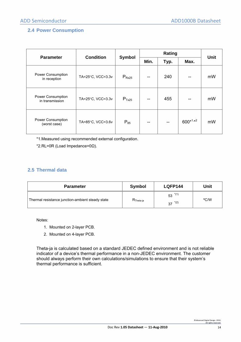
2.4 Power Consumption
Parameter Condition Symbol Rating
Unit Min. Typ. Max.
Power Consumption in reception TA=25°C, VCC=3.3v PRx25 -- 240 -- mW
Power Consumption in transmission TA=25°C, VCC=3.3v PTx25 -- 455 -- mW
Power Consumption (worst case) TA=85°C, VCC=3.6v P85 -- -- 600*1,*2 mW
*1.Measured using recommended external configuration.
*2.RL=0R (Load Impedance=0Ω).
2.5 Thermal data
Parameter Symbol LQFP144 Unit
Thermal resistance junction-ambient steady state RTheta-ja 53 *(1)
ºC/W 37 *(2)
Notes:
1. Mounted on 2-layer PCB.
2. Mounted on 4-layer PCB.
Theta-ja is calculated based on a standard JEDEC defined environment and is not reliable indicator of a device’s thermal performance in a non-JEDEC environment. The customer should always perform their own calculations/simulations to ensure that their system’s thermal performance is sufficient.
ADD Semiconductor ADD1000B Datasheet
©Advanced Digital Design. 2010. All rights reserved.
Doc Rev 1.05 Datasheet — 11‐Aug‐2010 15
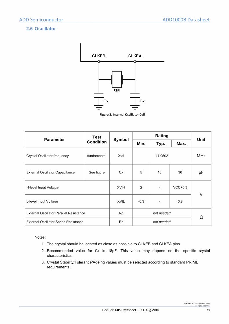
2.6 Oscillator
Figure 3. Internal Oscillator Cell
Parameter Test Condition Symbol
Rating Unit
Min. Typ. Max.
Crystal Oscillator frequency fundamental Xtal 11.0592 MHz
External Oscillator Capacitance See figure Cx 5 18 30 pF
H-level Input Voltage XVIH 2 - VCC+0.3
V L-level Input Voltage XVIL -0.3 - 0.8
External Oscillator Parallel Resistance Rp not needed Ω
External Oscillator Series Resistance Rs not needed
Notes:
1. The crystal should be located as close as possible to CLKEB and CLKEA pins.
2. Recommended value for Cx is 18pF. This value may depend on the specific crystal characteristics.
3. Crystal Stability/Tolerance/Ageing values must be selected according to standard PRIME requirements.

ADD Semiconductor ADD1000B Datasheet
©Advanced Digital Design. 2010. All rights reserved.
Doc Rev 1.05 Datasheet — 11‐Aug‐2010 16
Figure 4. Internal Oscillator Cell
ADD Semiconductor ADD1000B Datasheet
©Advanced Digital Design. 2010. All rights reserved.
Doc Rev 1.05 Datasheet — 11‐Aug‐2010 17
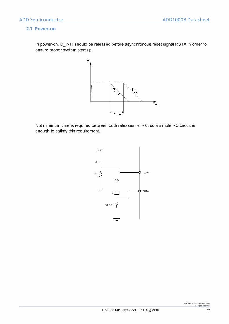
2.7 Power-on
In power-on, D_INIT should be released before asynchronous reset signal RSTA in order to ensure proper system start up.
Not minimum time is required between both releases, Δt > 0, so a simple RC circuit is enough to satisfy this requirement.
3.3v
3.3v
C
C
R1
R2 > R1
D_INIT
RSTA

ADD Semiconductor ADD1000B Datasheet
©Advanced Digital Design. 2010. All rights reserved.
Doc Rev 1.05 Datasheet — 11‐Aug‐2010 18
3. Mechanical data
144-pin plastic LQFP (16x16mm) Pb-free, RoHS compliant. Ambient Temperature Range: -40ºC to +85ºC. Ordering Code: ADD1000BQF144
ADD Semiconductor ADD1000B Datasheet
©Advanced Digital Design. 2010. All rights reserved.
Doc Rev 1.05 Datasheet — 11‐Aug‐2010 19
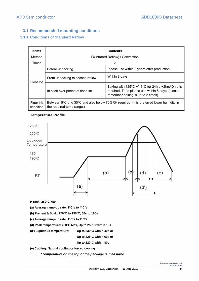
3.1 Recommended mounting conditions 3.1.1 Conditions of Standard Reflow
Items Contents
Method IR(Infrared Reflow) / Convection
Times 2
Floor life
Before unpacking Please use within 2 years after production
From unpacking to second reflow Within 8 days
In case over period of floor life Baking with 125°C +/- 3°C for 24hrs +2hrs/-0hrs is required. Then please use within 8 days. (please remember baking is up to 2 times)
Floor life condition
Between 5°C and 30°C and also below 70%RH required. (It is preferred lower humidity in the required temp range.)
Temperature Profile
H rank: 260°C Max
(a) Average ramp-up rate: 1°C/s to 4°C/s
(b) Preheat & Soak: 170°C to 190°C, 60s to 180s
(c) Average ramp-un rate: 1°C/s to 4°C/s
(d) Peak temperature: 260°C Max, Up to 255°C within 10s
(d’) Liquidous temperature: Up to 230°C within 40s or
Up to 225°C within 60s or
Up to 220°C within 80s
(e) Cooling: Natural cooling or forced cooling
*Temperature on the top of the package is measured
ADD Semiconductor ADD1000B Datasheet
©Advanced Digital Design. 2010. All rights reserved.
Doc Rev 1.05 Datasheet — 11‐Aug‐2010 20
3.1.2 Manual Soldering
Items Contents
Floor life
Before unpacking Please use within 2 years after production
From unpacking to Manual Soldering Within 2 years after production (No control required for moisture adsorption because it is partial heating)
Floor life condition
Between 5°C and 30°C and also below 70%RH required. (It is preferred lower humidity in the required temp range.)
Solder Condition
Temperature of soldering iron: Max 400°C, Time: Within 5 seconds/pin
*Be careful for touching package body with iron
ADD Semiconductor ADD1000B Datasheet
©Advanced Digital Design. 2010. All rights reserved.
Doc Rev 1.05 Datasheet — 11‐Aug‐2010 21
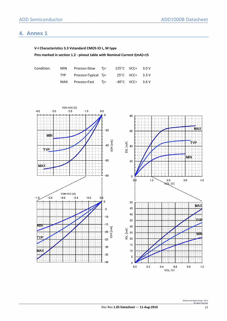
4. Annex 1
V‐I Characteristics 3.3 Vstandard CMOS IO L, M type
Pins marked in section 1.2 ‐ pinout table with Nominal Current I(mA)=±5
Condition: MIN Process= Slow Tj= 125°C VCC= 3.0 V
TYP Process=Typical Tj= 25°C VCC= 3.3 V
MAX Process=Fast Tj= ‐40°C VCC= 3.6 V

ADD Semiconductor ADD1000B Datasheet
©Advanced Digital Design. 2010. All rights reserved.
Doc Rev 1.05 Datasheet — 11‐Aug‐2010 22
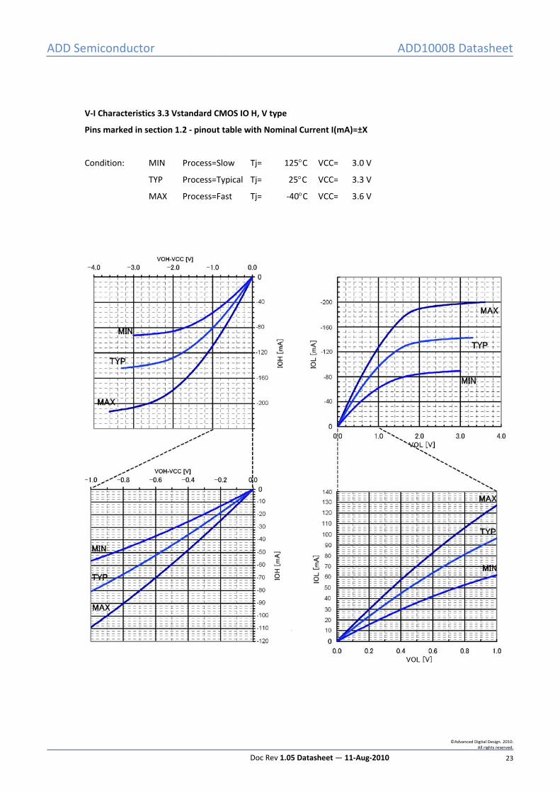
V‐I Characteristics 3.3 Vstandard CMOS IO H, V type
Pins marked in section 1.2 ‐ pinout table with Nominal Current I(mA)=±10
Condition: MIN Process= Slow Tj= 125°C VCC= 3.0 V
TYP Process=Typical Tj= 25°C VCC= 3.3 V
MAX Process=Fast Tj= ‐40°C VCC= 3.6 V
ADD Semiconductor ADD1000B Datasheet
©Advanced Digital Design. 2010. All rights reserved.
Doc Rev 1.05 Datasheet — 11‐Aug‐2010 23
V‐I Characteristics 3.3 Vstandard CMOS IO H, V type
Pins marked in section 1.2 ‐ pinout table with Nominal Current I(mA)=±X
Condition: MIN Process= Slow Tj= 125°C VCC= 3.0 V
TYP Process=Typical Tj= 25°C VCC= 3.3 V
MAX Process=Fast Tj= ‐40°C VCC= 3.6 V

ADD Semiconductor
ADD1000B Datasheet
Preliminary
©Advanced Digital Design. 2010.
All rights reserved.
Doc Rev 1.05 Datasheet — 11‐Aug‐2010 24 of 26
5. Annex 2
5.1 ADD1000B Application circuit example
VCC2
GND3
GND4
GND5
TDI6
TDO7
TCK8
TMS9
TRST10
D_INIT11
RSTA12
PROG13
SECURED14
EW15
DEBUG16
VDD 89
VCC17
CLKEB18
GND19
CLKEA20
VCC21
GND22
GND23
VDE024
VDE025
VSS026
LDO_PD27
VDD28
GND29
VCC30
VREF131
VREF232
VNR33
TRIAC334
TRIAC235
TRIA
C037
P55/
TXD
1/IN
TA1
38
P54/
RXD
1/IN
TA0
39
P47/
T2EX
/INTA
340
P46/
T2/I
NTA
241
P17/
SSN
42
VCC
43
GN
D44
EMIT
045
EMIT
146
EMIT
247
VCC
48
GN
D49
EMIT
350
EMIT
451
EMIT
552
EMIT
653
VCC
54
GN
D55
EMIT
756
EMIT
857
EMIT
958
EMIT
1059
VCC
60
GN
D61
EMIT
1162
EMIT
1263
VCC
64
GN
D65
P31/
TXD
066
P30/
RXD
067
P45/
MIS
O1/
INTB
368
P44/
MO
SI1/
INTB
269
P43/
SPIC
LK1/
INTB
170
P42/
SS1/
INTB
071
P40/RXD2 73VCC 74GND 75INTC3 76INTC2 77INTC1 78INTC0 79NC 80NC 81NC 82NC 83NC 84NC 85NC 86NC 87NC 88
VCC 90GND 91NC 92NC 93NC 94NC 95NC 96NC 97NC 98NC 99NC 100NC 101NC 102VCC 103GND 104INTD3 105INTD2 106INTD1 107INTD0 108
NC
111
NC
112
GN
D11
3D
C_CO
MP
114
VCC
115
ENA
BLE
116
GN
D11
7D
NIN
118
DIN
119
REC1
120
REC2
121
REC3
122
REC4
123
REC5
124
REC6
125
REC7
126
REC8
127
VCC
128
GN
D12
9V
RL13
0V
IN13
1V
RH13
2A
VD
113
3A
VS1
134
AV
D2
135
AV
S213
6V
CC13
7G
ND
138
P53/
MIS
O0
139
P52/
MO
SI0
140
P51/
SPIC
LK0
141
P50/
SS0
142
P35/
T114
3P3
4/T0
144
P33/INT11
TRIAC136
P41/
TXD
272
NC
109
NC
110
U51ADD1000B
P34/T0P35/T1
P46/
T2
P43/
SPIC
LK1
P40/RXD2
P42/
SS1
DEBUG
P47/
T2EX
P31/
TXD
0P3
0/RX
D0
P45/
MIS
O1
P41/
TXD
2
P44/
MO
SI1
PROG
P55/
TXD
1P5
4/R
XD
1
P33
VCC
VCCC70100nF
C69100nF
C67100nF
C60100nF
C59100nF
C58100nF
C73100nF
C72100nF
C71100nF
C80100nF
C78100nF
C77100nF
C76100nF
C75100nF
C6110uF
R5310K
VCC
C6210uF
R541K
VCC
VCC
R57NM
R560R
VCC1
2Y50
11.0592MHz
C63
18pF
C65
18pF
C66
10uF
C64
10uF
C7410uF
C7910uF
R50180R
R51120R
VCC
R52
0RC5310uF
C54100nF
VCC VCCF
C55100nF
VCC
WESECURED
RESET
SI5
SCK6
CS1
WP3
RESET7
SO 2
VCC 8
VSS 4
U50M25PE40
SS0
SPIC
LK0
MO
SI0
MIS
O0
MISO0
VCCC50100nF
MOSI0SPICLK0SS0
VCC
GND2 DQ 1U52
DS2401X1
D50
GREEN
R59
220R
VCC
TXR
X
R58 0RVCC
W50
Jumper
R551K
VCC
C56100nF
C57100nF
C68100nF
C52100nF
C51100nF
VCCF
VRH VRL
RESET
P34/T0P35/T1
P40/RXD2
P42/
SS1
P33
P31/
TXD
0P3
0/RX
D0
P45/
MIS
O1
P41/
TXD
2
P44/
MO
SI
PROG
PLCT
X
PLCRX
TXRX
DEBUG
PLCT
X
VNRTRIAC3TRIAC2TRIAC1
TRIA
C0
VNR
TRIA
C0
TRIAC1TRIAC2TRIAC3
R60
4K7
VCC
Optional
INTC0INTC1INTC2INTC3
INTC0INTC1INTC2INTC3
PLCRX
R73 10KVCC
R74 10K
INTD0 INTD0INTD1INTD2INTD3
INTD1INTD2INTD3
W51
Jumper
R61
120R
ADD Semiconductor
ADD1000B Datasheet
Preliminary
©Advanced Digital Design. 2010.
All rights reserved.
Doc Rev 1.05 Datasheet — 11‐Aug‐2010 25 of 26
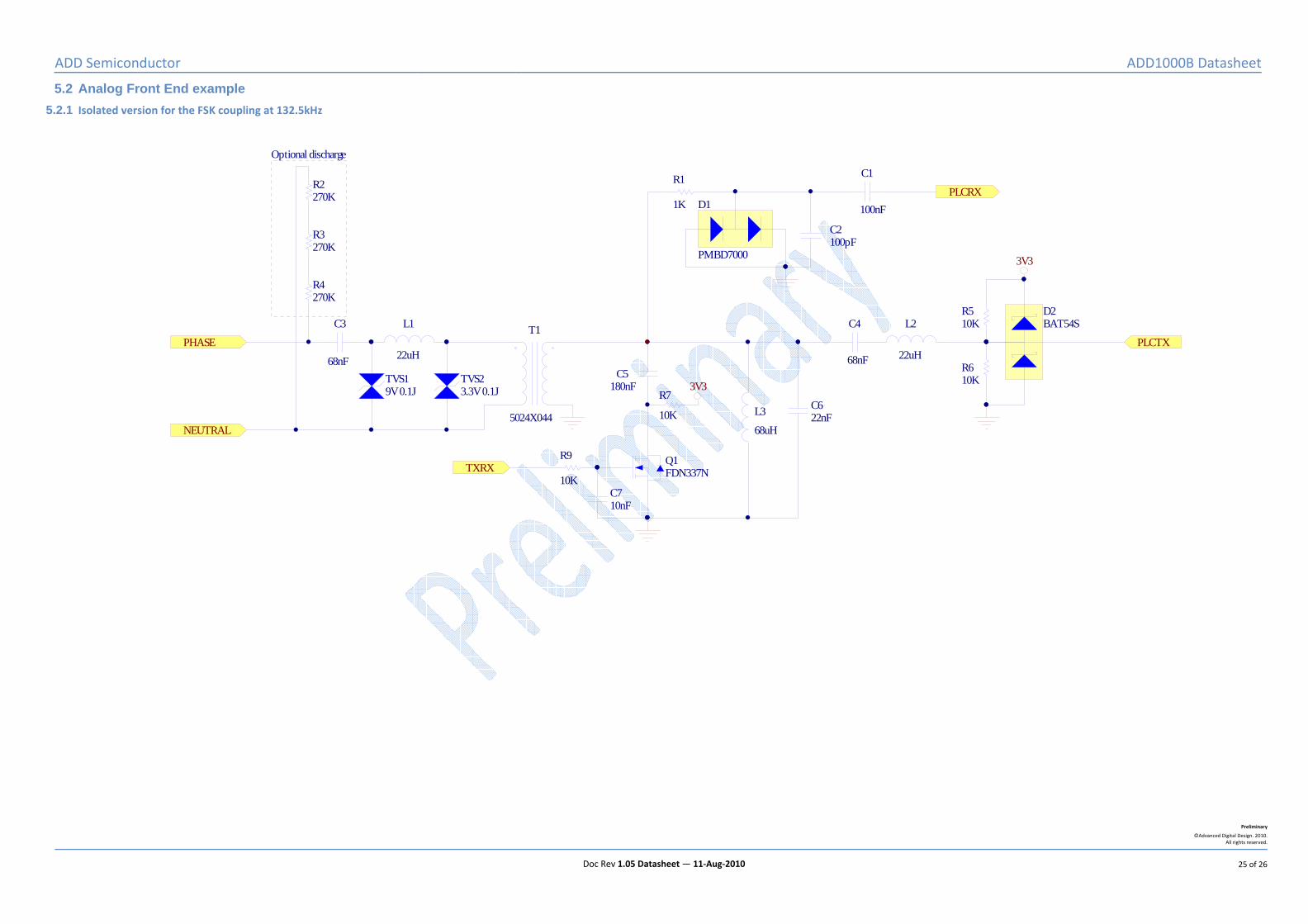
5.2 Analog Front End example 5.2.1 Isolated version for the FSK coupling at 132.5kHz
PLCRX
PLCTXPHASE
NEUTRAL
R510K
3V3
R610K
R7
10K
3V3
R1
1K
C1
100nF
C2100pF
D2BAT54ST1
5024X044 L3
68uH
D1
PMBD7000
TXRX
R3270K
R4270K
R2270K
Optional discharge
C3
68nF
L1
22uH
C5180nF
C622nF
C4
68nF
L2
22uH
Q1FDN337N
R9
10K
TVS23.3V 0.1J
TVS19V 0.1J
C710nF
ADD Semiconductor
ADD1000B Datasheet
Preliminary
©Advanced Digital Design. 2010.
All rights reserved.
Doc Rev 1.05 Datasheet — 11‐Aug‐2010 26 of 26
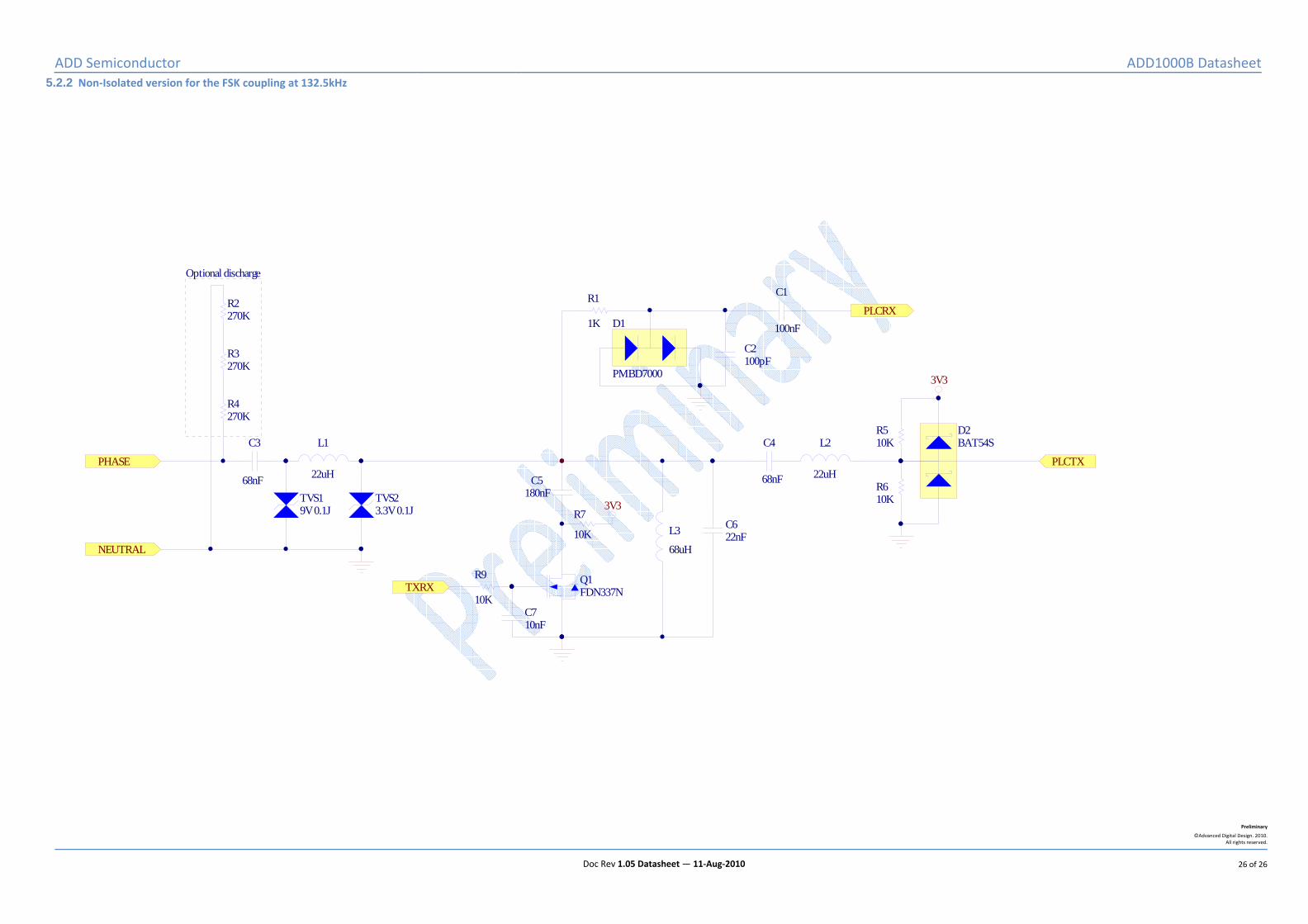
5.2.2 Non‐Isolated version for the FSK coupling at 132.5kHz
PLCRX
PLCTXPHASE
NEUTRAL
R510K
3V3
R610K
R7
10K
3V3
R1
1K
C1
100nF
C2100pF
D2BAT54S
L3
68uH
D1
PMBD7000
TXRX
R3270K
R4270K
R2270K
Optional discharge
C3
68nF
L1
22uH C5180nF
C622nF
C4
68nF
L2
22uH
Q1FDN337N
R9
10K
TVS23.3V 0.1J
TVS19V 0.1J
C710nF