ana margarida rocha defeitos de irradiação em estruturas ... · extinção da luminescência com...
TRANSCRIPT

Univ ersidade de Av eiro2011
Departamento de Física
Ana Margarida Rocha de Oliveira Cavaco
Defeitos de Irradiação em Estruturas Quânticas de Semicondutores A 3B5
Radiation-Induced Defects in Quantum-Size Structures of A 3B5 Semiconductors

Univ ersidade de Av eiro2011
Departamento de Física
Ana Margarida Rocha de Oliveira Cavaco
Defeitos de Irradiação em Estruturas Quânticas de Semicondutores A 3B5
Radiation-Induced Defects in Quantum-Size Structures of A 3B5 Semiconductors
Dissertação apresentada à Universidade de Aveiro para cumprimento dos requisitos necessários à obtenção do grau de Doutor em Física, realizada sob a orientação científica da Professora Doutora Maria Celeste do Carmo, Professora Catedrática do Departamento de Física da Universidade de Aveiro e do Professor Doutor Nikolai Andreevich Sobolev, Professor Associado do Departamento de Física da Universidade de Aveiro.
Apoio financeiro da FCT no âmbito da bolsa SFRH/BD/1264/2000. Financially supported by FCT in the framework of the bursary SFRH/BD/1264/2000.

o júri
presidente Doutor José Manuel Lopes da Silva Moreira professor catedrático da Universidade de Aveiro
Doutor Axel Hoffmann professor catedrático do Instituto de Física do Estado Sólido da Universidade Técnica de Berlim, Alemanha
Doutor Mikhail Igorevich Vasilevskiy professor catedrático da Universidade do Minho
Doutor Eduardo Jorge da Costa Alves investigador principal, coordenador da Unidade de Física e Aceleradores do Instituto Tecnológico e Nuclear
Doutora Maria Celeste da Silva Carmo professora catedrática da Universidade de Aveiro
Doutor Nikolai Andreevich Sobolev professor associado da Universidade de Aveiro

To my husband and daughter,
Cavaco and Ana Filipe;
To my parents,
Vitor and Jãe;
And my brother,
Rui.

Não é o desafio
que define quem somos
nem o que somos capazes de fazer.
O que nos define é o modo
como enfrentamos esse desafio.
Richard Bach
Nada ao Acaso
.

ackno wledgments
I would like to start by saying that during the last years many people contributed to the development of this thesis. I would like to thank to some of them explicitly, and apologize to all those who should also been mentioned. First of all, I want to thank Professor Celeste Carmo and Professor Nikolai Sobolev for the opportunity to develop this work being supervised by both, for the confidence and support. To Professor Dieter Bimberg and Professor Axel Hoffmann from the Institute of Solid State Physics of the Technical University of Berlin for the possibility of developing experimental work within the Institute and for the supply of samples, and to all research group, namely Robert Heitz†, Frank Heinrichsdorff, Harald Born, Sven Rodt, Roman Sellin and Florian Guffarth. To Professor Marius Grundmann from the Institute of Experimental Physics II of the University of Leipzig and his group, namely Jens Bauer and Marc Schillgalies, for fruitful discussions and the opportunity to perform experimental work within the group. I enjoyed a very fruitful cooperation with Professor Mikhail Vasilevskiy and Adil Chahboun from the Physics Department of the University of Minho and Dr. Nikolay Baidus from N.I. Lobachevsky State University from Nizhni Novgorod. My regards to them and thanks for supplying the samples. Many friends and colleagues have contributed with their companionship during these years. My special thanks to Rosário and Clarisse. To all my friends outside university for their steady support, friendship and patience in the past ten years and all my entire life. My special thanks to Maria and Bi. I gratefully acknowledge a personal grant over a period of four years from the “Fundação para a Ciência e a Tecnologia” and additional travel support in several cases.

palavras-chave
semicondu ctores, es tru turas quâ ntic as, defei tos de irradiaçã o, espec tro sco pia óptica
resumo
As estruturas quânticas de semicondutores, nomeadamente baseadas em GaAs, têm tido nos últimos vinte anos um claro desenvolvimento. Este desenvolvimento deve-se principalmente ao potencial tecnológico que estas estruturas apresentam. As aplicações espaciais, em ambientes agressivos do ponto de vista do nível de radiação a que os dispositivos estão sujeitos, motivaram todo o desenrolar de estudos na área dos defeitos induzidos pela radiação. As propriedades dos semicondutores e dos dispositivos de semicondutores são altamente influenciadas pela presença de defeitos estruturais, em particular os induzidos pela radiação. As propriedades dos defeitos, os processos de criação e transformação de defeitos devem ser fortemente alterados quando se efectua a transição entre o semicondutor volúmico e as heteroestruturas de baixa dimensão. Este trabalho teve como principal objectivo o estudo de defeitos induzidos pela radiação em estruturas quânticas baseadas em GaAs e InAs. Foram avaliadas as alterações introduzidas pelos defeitos em estruturas de poços quânticos e de pontos quânticos irradiadas com electrões e com protões. A utilização de várias técnicas de espectroscopia óptica, fotoluminescência, excitação de fotoluminescência e fotoluminescência resolvida no tempo, permitiu caracterizar as diferentes estruturas antes e após a irradiação. Foi inequivocamente constatada uma maior resistência à radiação dos pontos quânticos quando comparados com os poços quânticos e os materiais volúmicos. Esta resistência deve-se principalmente a uma maior localização da função de onda dos portadores com o aumento do confinamento dos mesmos. Outra razão provável é a expulsão dos defeitos dos pontos quânticos para a matriz. No entanto, a existência de defeitos na vizinhança dos pontos quânticos promove a fuga dos portadores dos níveis excitados, cujas funções de onda são menos localizadas, provocando um aumento da recombinação não-radiativa e, consequentemente, uma diminuição da intensidade de luminescência dos dispositivos. O desenvolvimento de um modelo bastante simples para a estatística de portadores fora de equilíbrio permitiu reproduzir os resultados de luminescência em função da temperatura. Os resultados demonstraram que a extinção da luminescência com o aumento da temperatura é determinada por dois factores: a redistribuição dos portadores minoritários entre os pontos quânticos, o poço quântico e as barreiras de GaAs e a diminuição na taxa de recombinação radiativa relacionada com a dependência, na temperatura, do nível de Fermi dos portadores maioritários.

keywords
semicondu ctors, quan tum-size s truc tures, ra diati on-induc ed defects, optical spe ctroscopy
abstract
Quantum size semiconductor structures, namely those based on GaAs, have experienced an outstanding development in the past twenty years. This development is mainly due to the technological potential these structures present. Space-based telecommunications in harsh radiation environments motivated a run off of studies in the field of radiation-induced defects. Semiconductor properties and semiconductor device performance are highly influenced by the presence of structural defects, particularly those induced by irradiation. Properties as well as processes of creation and transformation of defects are expected to be substantially modified when moving from a bulk semiconductor to corresponding low-dimensionality structures. The main goal of this work was to study the radiation-induced defects in quantum-size heterostructures composed of GaAs and InAs. The changes introduced by radiation defects have been evaluated in structures comprising quantum dots and quantum wells subjected to irradiation with electron and protons. The use of several optical spectroscopy techniques, namely photoluminescence, photoluminescence excitation and time-resolved photoluminescence, allowed the characterization of different structures in the as-grown and irradiated state. A higher radiation hardness of the quantum dots as compared to quantum wellsand corresponding bulk materials has been clearly established. This higher resistance is mainly due to the higher localization of the carrier wavefunction with increasing confinement. Another probable reason is the expulsion of mobile defects into the surrounding barrier material. However, the existence of defects in the neighbourhood of the quantum dots promotes tunnel escape of carriers from the excited dot states, whose wavefunctions are less localized, to the defects, causing an increase in the non-radiative recombination and, consequently, a decrease in device luminescence. A rather simple model for the carrier statistics out of equilibrium which reproduces quite well the luminescence results as a function of temperature allowed to demonstrate that the quantum dot photoluminescence quenching with increasing temperature is determined by two factors: the minority carrier redistribution between the quantum dots, quantum well and GaAs barriers, and the decrease in the radiative recombination rate related to the temperature dependence of the Fermi level of the majority carriers.

List of publications
A. Chahboun, M.I. Vasilevskiy, N.V. Baidus, A. Cavaco, N.A. Sobolev, M.C. Carmo,
E. Alves, B.N. Zvonkov, “Further insight into the temperature quenching of
photoluminescence from InAs/GaAs self-assembled quantum dots”, Jour-
nal of Applied Physics 103, 083548 (2008).
A. Chahboun, N. V. Baidus, P. B. Demina, B. N. Zvonkov, M. J. M. Gomes, A. Cavaco,
N. A. Sobolev, M. C. Carmo, and M. I. Vasilevskiy, “Influence of matrix defects
on the photoluminescence of InAs self-assembled quantum dots”, Physica
Status Solidi (a) 203, 1348-1352 (2006).
A. Cavaco, M.C. Carmo, N.A. Sobolev, F. Guffarth, H. Born, R. Heitz, A. Hoffmann, D.
Bimberg, “Intradot carrier relaxation in radiation-damaged InGaAs/GaAs
quantum dot heterostructures”, in: Physics, Chemistry and Application of Nanos-
tructures, World Scientific (Singapore), p.111 (2003).
A. Cavaco, N.A. Sobolev, M.C. Carmo, F. Guffarth, H. Born, R. Heitz, A. Hoffmann, D.
Bimberg, “Carrier dynamics in particle-irradiated InGaAs/GaAs quantum
dots”, Physica Status Solidi (c) 0, 1177 (2003).
N.A. Sobolev, A. Cavaco, M.C. Carmo, M. Grundmann, F. Heinrichsdorff, D. Bimberg,
“Enhanced Radiation Hardness of InAs/GaAs Quantum Dot Structures”,
Physica Status Solidi (b) 224 (1), 93 (2001).
N.A. Sobolev, A. Cavaco, M.C. Carmo, H. Born, M. Grundmann, F. Heinrichsdorff,
R. Heitz. A. Hoffmann, D. Bimberg, “Influence of electron irradiation on car-
rier recombination and intradot relaxation in InGaAs/GaAs quantum dot
i

ii
structures”, in: Physics, Chemistry and Application of Nanostructures, World Sci-
entific (Singapore), p.146 (2001).

List of symbols and acronyms
2D Two-Dimensional
3D Three-Dimensional
AFM Atomic Force Microscopy
AlAs Aluminium Arsenide
AlGaAs Aluminium Gallium Arsenide
AP-MOVPE Atmospheric Pressure Metal-Organic Vapour Phase Epitaxy
Ar Argon
Asi Arsine Interstitial
CCl4 Tetrachloromethane
CdSe Cadmium Selenide
CL Cap layer
CQW Coupled Quantum Wells
CW Continuous wave
EBIC Electron Beam Induced Current
FTIR Fourier Transform Infrared
FWHM Full Width at Half Maximum
GaAs Gallium Arsenide
Gai Gallium Interstitial
GaSb Gallium Antimonide
Ge Germanium
GS Ground State
He Helium
He-Ne Helium-Neon
InAs Indium Arsenide
InGaAs Indium Gallium Arsenide
InGaAsP Indium Gallium Arsine Phosphide
InP Indium Phosphide
iii

iv
InSb Indium Antimonide
LD Laser Diode
LED Light Emitting Diode
LO Longitudinal Optical
MBE Molecular Beam Epitaxy
MCP Multi-channel Plate
ML Monolayer
Mn Manganese
MOCVD Metal-Organic Chemical Vapour Deposition
OPO Optical Parametric Oscillator
PD Photodiode
PL Photoluminescence
PLE Photoluminescence Excitation
QD Quantum Dot
QW Quantum Well
QWR Quantum Wire
RHEED Reflection High-Energy Electron Diffraction
RT Room Temperature
SAQD Self-Assembled Quantum Dot
Si Silicon
SK Stranski-Krastanow
SRIM Stopping and Range of Ions in Matter
Te Tellurium
TEGa Triethylgallium
TEM Transmission Electron Microscopy
Ti Titanium
TMAl Trimethylaluminium
TMGa Trimethylgallium
TMIn Trimethylindium
TRIM Transport of Ions in Matter
TRPL Time-Resolved Photoluminescence
TU Technical University
UHV Ultra-High Vacuum
UV Ultra-Violet
VAs Arsine Vacancy
VGa Gallium Vacancy

v
V-I Vacancy-Interstitial
VCSEL Vertical-Cavity Surface-Emitting Laser
WL Wetting Layer
XSTM Cross-sectional Scanning Tunnelling Microscopy

vi

List of Figures
2.1 Zincblende structure . . . . . . . . . . . . . . . . . . . . . . . . . . . . 6
2.2 Band offsets . . . . . . . . . . . . . . . . . . . . . . . . . . . . . . . . . 8
2.3 Density of states for charge carriers in structures with different dimen-
sionality . . . . . . . . . . . . . . . . . . . . . . . . . . . . . . . . . . . 9
2.4 Schematic representation of energy levels in a single atom, a bulk semi-
conductor and a quantum dot . . . . . . . . . . . . . . . . . . . . . . . 10
2.5 Variation of the formation energy of a substitutional Mn impurity in a
CdSe nanocrystal as a function of the nanocrystal diameter . . . . . . . 14
2.6 Changes in minority-carrier diffusion length . . . . . . . . . . . . . . . 15
2.7 Maximum and average energy transmitted to a silicon atom as a function
of the incident energy for electrons, protons and neutrons . . . . . . . . 16
2.8 TRIM simulations of the depth distribution of the displaced target atoms
and implanted atoms . . . . . . . . . . . . . . . . . . . . . . . . . . . . 17
2.9 Simulation of the penetration of hydrogen atoms in GaAs . . . . . . . . 18
3.1 Different growth modes of crystal epilayers on lattice-mismatched sub-
strates . . . . . . . . . . . . . . . . . . . . . . . . . . . . . . . . . . . . 24
3.2 Schematic diagram of a MOCVD growth reactor used for III-V semicon-
ductors growth. . . . . . . . . . . . . . . . . . . . . . . . . . . . . . . . 25
3.3 Simplified schematic of the MOCVD setup of the Aix machine used at
the Institute of Solid State Physics of the Technical University of Berlin,
Germany . . . . . . . . . . . . . . . . . . . . . . . . . . . . . . . . . . . 29
vii

viii LIST OF FIGURES
3.4 Scheme of doping from a bulk elementary source by pulsed laser sputter-
ing in AP-MOVPE process used at the University of Nizhny Novgorod,
Russia . . . . . . . . . . . . . . . . . . . . . . . . . . . . . . . . . . . . 30
3.5 Experimental setup for PL measurements using a grating spectrometer 33
3.6 Experimental setup for PL measurements using a Fourier transform in-
frared spectrometer . . . . . . . . . . . . . . . . . . . . . . . . . . . . . 34
3.7 Diagram illustrating the photon energy ranges of the sources available
for resonant excitation . . . . . . . . . . . . . . . . . . . . . . . . . . . 37
3.8 Schematic representation of the setup used at the Institute of Solid State
Physics of the Technical University of Berlin for the PLE experiments . 38
3.9 Schematic representation of the setup used, at the Institute of Solid State
Physics of the Technical University of Berlin, for the TRPL experiments 39
3.10 The infrared laser system, at the Institute of Solid State Physics of the
Technical University of Berlin, for the TRPL experiments . . . . . . . . 40
4.1 Layer sequence of the laser structure samples . . . . . . . . . . . . . . . 45
4.2 PL spectra of laser heterostructures samples . . . . . . . . . . . . . . . 46
4.3 Gaussian fit of QD PL peak . . . . . . . . . . . . . . . . . . . . . . . . 47
4.4 Temperature dependence of the PL characteristics for the as-grown sam-
ples 1×QD, CQW and 5×QD . . . . . . . . . . . . . . . . . . . . . . . 48
4.5 Layer sequence of the samples with non-uniform WL thickness . . . . . 50
4.6 Plan view TEM image of sample TU3581. . . . . . . . . . . . . . . . . 51
4.7 PL spectrum of the as-grown sample TU5330 taken at 10 K . . . . . . 52
4.8 PL spectrum of the as-grown sample TU5330 taken at 70 K . . . . . . 52
4.9 PL spectrum of the as-grown sample TU5330 taken at 300 K . . . . . . 53
4.10 PL spectra of the as-grown sample TU4738 . . . . . . . . . . . . . . . . 54
4.11 PL spectra of non-uniform WL thickness samples taken at 10 K . . . . 55
4.12 PL and PLE spectra and contour plot of the as-grown sample TU5330
taken at 7 K . . . . . . . . . . . . . . . . . . . . . . . . . . . . . . . . . 56

LIST OF FIGURES ix
4.13 Temperature dependence of the integrated PL intensity for different
identified QD and WL emissions for the as-grown sample TU5330. . . . 57
4.14 Layer sequence of the sample TU5411 . . . . . . . . . . . . . . . . . . . 58
4.15 PL spectrum of the as-grown sample TU5411 taken at 10 K . . . . . . 59
4.16 PL spectrum of the as-grown sample TU5411 taken at 300 K . . . . . . 59
4.17 PL spectrum of the as-grown sample TU5411 taken at 300 K . . . . . . 60
4.18 Layer sequence of the samples with different cap layer thicknesses . . . 61
4.19 PL spectra of thin cap layer samples . . . . . . . . . . . . . . . . . . . 62
4.20 QD ground state transition energy at room temperature vs. GaAs cap
layer thickness. . . . . . . . . . . . . . . . . . . . . . . . . . . . . . . . 63
4.21 Temperature dependence results of sample, NN3760, with 10 nm cap
layer thickness . . . . . . . . . . . . . . . . . . . . . . . . . . . . . . . . 64
4.22 PL spectra of thin cap layer samples with different QW thickness and
In content in QW . . . . . . . . . . . . . . . . . . . . . . . . . . . . . . 65
4.23 PL spectra of thin cap layer samples with different QW thickness and
In content in QW . . . . . . . . . . . . . . . . . . . . . . . . . . . . . . 66
4.24 PLE spectra of samples with different cap layer thickness . . . . . . . . 67
4.25 PL and PLE spectra of thin cap layer samples with different QW In
content . . . . . . . . . . . . . . . . . . . . . . . . . . . . . . . . . . . . 68
4.26 Layer sequence of the samples from CCl4 treatment . . . . . . . . . . . 69
4.27 PL spectra of samples from the # 41 series taken at 12 K . . . . . . . . 70
4.28 PL spectra of two similar samples taken at 12 K, showing the influence
of the CCl4 treatment on the QD PL emission. . . . . . . . . . . . . . . 71
4.29 Temperature dependence of the QD PL emission from samples of the #
41 series. Sample characteristics and labels are according to table 4.2 . 71
5.1 FTIR PL spectra of samples 1×QD, CQW and 5×QD measured at 10 K 80
5.2 PL spectra of samples 1×QD, CQW and 5×QD after irradiation . . . . 82
5.3 Plots of k/k0 vs. electron irradiation fluence for the laser structure samples 83

x LIST OF FIGURES
5.4 Plots of k/k0 vs. electron irradiation fluence for the laser structure sam-
ples at different temperatures . . . . . . . . . . . . . . . . . . . . . . . 84
5.5 PL spectra of the as-grown sample TU3904 (1×QD) taken at 10 K for
several excitation powers. . . . . . . . . . . . . . . . . . . . . . . . . . . 85
5.6 Linear fit of the integrated PL intensity vs. excitation power for the
as-grown sample TU3904 in order to determine the parameter k. . . . . 85
5.7 PL spectra of sample TU5330 taken at 10 K after irradiation . . . . . . 86
6.1 Schematic diagram illustrating carrier capture from GaAs barrier into a
QD via the wetting layer and carrier relaxation within the QD. . . . . . 92
6.2 Rise and decay times from TRPL measurements of sample TU5411. . . 96
6.3 PL and PLE spectra of sample TU5411. . . . . . . . . . . . . . . . . . 97
6.4 PL and PLE spectra of sample TU5330. . . . . . . . . . . . . . . . . . 99
6.5 Contour plots of the QD PL intensity for the as-grown and proton-
irradiated sample TU5330. . . . . . . . . . . . . . . . . . . . . . . . . . 100
6.6 PL transients taken at 2 K of the as-grown and electron-irradiated samples102
6.7 PL transients taken at 2 K of as-grown and electron-irradiated samples
upon resonant excitation . . . . . . . . . . . . . . . . . . . . . . . . . . 103
6.8 PLE spectra of sample 1×QD for various electron irradiation fluences . 104
7.1 Temperature dependence, from 10 to 300 K, of the PL of samples 1×QD
(TU3904), as-grown and irradiated . . . . . . . . . . . . . . . . . . . . 110
7.2 Arrhenius plots of the PL intensity for samples 1×QD (TU3904), as-
grown and irradiated. The irradiation fluence is indicated on the graph. 111
7.3 PL spectra of QD/QW heterostructures: NN4190 and NN4184 . . . . . 112
7.4 Temperature dependence of the integrated PL intensity for an as-grown
and two proton-irradiated NN4190 samples. . . . . . . . . . . . . . . . 113
7.5 Temperature dependence of the integrated PL intensity for an as-grown
and two proton-irradiated NN4184 samples. . . . . . . . . . . . . . . . 114
7.6 Temperature dependence of the integrated PL intensity for the as-grown
NN4190 samples for two different excitation densities. . . . . . . . . . . 114

LIST OF FIGURES xi
7.7 Model band structure of the GaAs/GaInAs(QW)/InAs(QD) heterostruc-
ture. . . . . . . . . . . . . . . . . . . . . . . . . . . . . . . . . . . . . . 116
7.8 Temperature dependence of IQD and IQW calculated for several defect
concentrations . . . . . . . . . . . . . . . . . . . . . . . . . . . . . . . . 123
7.9 Temperature dependence of IQD and IQW calculated for for different
excitation intensities . . . . . . . . . . . . . . . . . . . . . . . . . . . . 124
7.10 Temperature dependence of IQD calculated for two different excitation
powers of a he-Ne laser and for resonant excitation through the QW . . 124

xii LIST OF FIGURES

List of Tables
2.1 Properties of GaAs and InAs . . . . . . . . . . . . . . . . . . . . . . . . 5
3.1 Major differences between MBE and MOCVD growth techniques . . . . 26
4.1 Sample characteristics . . . . . . . . . . . . . . . . . . . . . . . . . . . 60
4.2 Sample characteristics . . . . . . . . . . . . . . . . . . . . . . . . . . . 69
6.1 TRPL rise and decay times of proton-irradiated sample . . . . . . . . . 95
6.2 TRPL rise and decay times of electron-irradiated samples upon above-
bandgap excitation . . . . . . . . . . . . . . . . . . . . . . . . . . . . . 103
6.3 TRPL rise and decay times of electron-irradiated samples upon resonant
excitation . . . . . . . . . . . . . . . . . . . . . . . . . . . . . . . . . . 104
7.1 Material parameters used in the calculations . . . . . . . . . . . . . . . 122
xiii

xiv LIST OF TABLES

Contents
List of Publications i
List of symbols and acronyms iii
List of figures xi
List of tables xiii
1 Introduction 1
2 State of the art 5
2.1 Properties of InAs/GaAs heterostructures . . . . . . . . . . . . . . . . 5
2.1.1 GaAs and InAs . . . . . . . . . . . . . . . . . . . . . . . . . . . 5
2.1.2 Band offsets . . . . . . . . . . . . . . . . . . . . . . . . . . . . . 7
2.1.3 Density of states . . . . . . . . . . . . . . . . . . . . . . . . . . 8
2.1.4 Quantum Dots . . . . . . . . . . . . . . . . . . . . . . . . . . . 9
2.2 Irradiation defects in III-V semiconductors . . . . . . . . . . . . . . . . 11
2.2.1 Irradiation defects in quantum-size structures . . . . . . . . . . 14
2.2.2 Electron and proton irradiation . . . . . . . . . . . . . . . . . . 16
2.3 Resume . . . . . . . . . . . . . . . . . . . . . . . . . . . . . . . . . . . 19
Bibliography . . . . . . . . . . . . . . . . . . . . . . . . . . . . . . . . . 19
3 Sample growth and measurement techniques 23
xv

xvi CONTENTS
3.1 Growth . . . . . . . . . . . . . . . . . . . . . . . . . . . . . . . . . . . 23
3.1.1 Stranski-Krastanow growth mode . . . . . . . . . . . . . . . . . 24
3.1.2 MOCVD . . . . . . . . . . . . . . . . . . . . . . . . . . . . . . . 25
3.1.3 Samples growth . . . . . . . . . . . . . . . . . . . . . . . . . . . 28
3.2 Measurement techniques . . . . . . . . . . . . . . . . . . . . . . . . . . 31
3.2.1 Photoluminescence . . . . . . . . . . . . . . . . . . . . . . . . . 32
3.2.2 Photoluminescence excitation spectroscopy . . . . . . . . . . . . 36
3.2.3 Time-resolved photoluminescence . . . . . . . . . . . . . . . . . 39
3.3 Resume . . . . . . . . . . . . . . . . . . . . . . . . . . . . . . . . . . . 41
Bibliography . . . . . . . . . . . . . . . . . . . . . . . . . . . . . . . . . 41
4 Characterization of the as-grown samples 45
4.1 Laser structures . . . . . . . . . . . . . . . . . . . . . . . . . . . . . . . 45
4.2 Samples with non-uniform WL thickness . . . . . . . . . . . . . . . . . 49
4.3 TU5411: dots-in-a-well structure . . . . . . . . . . . . . . . . . . . . . 57
4.4 Other dots-in-a-well structures with different cap layer thicknesses . . . 60
4.5 Samples subjected to CCl4 treatment . . . . . . . . . . . . . . . . . . . 69
4.6 Conclusions . . . . . . . . . . . . . . . . . . . . . . . . . . . . . . . . . 72
Bibliography . . . . . . . . . . . . . . . . . . . . . . . . . . . . . . . . . 72
5 Radiation hardness 77
5.1 Introduction . . . . . . . . . . . . . . . . . . . . . . . . . . . . . . . . . 77
5.2 Radiation hardness of QDs and QWs . . . . . . . . . . . . . . . . . . . 79
5.2.1 k/k0 Representations . . . . . . . . . . . . . . . . . . . . . . . . 81
5.3 Non-uniform WL thickness samples . . . . . . . . . . . . . . . . . . . . 85
5.4 Mechanisms of radiation hardness . . . . . . . . . . . . . . . . . . . . . 86
5.5 Conclusions . . . . . . . . . . . . . . . . . . . . . . . . . . . . . . . . . 87
Bibliography . . . . . . . . . . . . . . . . . . . . . . . . . . . . . . . . . 88

CONTENTS xvii
6 Carrier recombination and intradot relaxation 91
6.1 Introduction . . . . . . . . . . . . . . . . . . . . . . . . . . . . . . . . . 91
6.2 Carrier dynamics . . . . . . . . . . . . . . . . . . . . . . . . . . . . . . 92
6.3 Equipment and measurement conditions . . . . . . . . . . . . . . . . . 93
6.4 Proton-irradiated samples . . . . . . . . . . . . . . . . . . . . . . . . . 94
6.4.1 Samples . . . . . . . . . . . . . . . . . . . . . . . . . . . . . . . 94
6.4.2 Results . . . . . . . . . . . . . . . . . . . . . . . . . . . . . . . . 94
6.4.3 Discussion . . . . . . . . . . . . . . . . . . . . . . . . . . . . . . 101
6.5 Electron-irradiated samples . . . . . . . . . . . . . . . . . . . . . . . . 101
6.5.1 Samples . . . . . . . . . . . . . . . . . . . . . . . . . . . . . . . 101
6.5.2 Results . . . . . . . . . . . . . . . . . . . . . . . . . . . . . . . . 102
6.5.3 Discussion . . . . . . . . . . . . . . . . . . . . . . . . . . . . . . 105
6.6 Conclusions . . . . . . . . . . . . . . . . . . . . . . . . . . . . . . . . . 106
Bibliography . . . . . . . . . . . . . . . . . . . . . . . . . . . . . . . . . 107
7 Influence of defects on the temperature dependence of the PL inten-
sity 109
7.1 Introduction . . . . . . . . . . . . . . . . . . . . . . . . . . . . . . . . . 109
7.2 Equipment and measurement conditions . . . . . . . . . . . . . . . . . 110
7.3 Experimental results . . . . . . . . . . . . . . . . . . . . . . . . . . . . 110
7.3.1 Laser structures . . . . . . . . . . . . . . . . . . . . . . . . . . . 110
7.3.2 Samples subjected to CCl4 treatment . . . . . . . . . . . . . . . 111
7.4 Model . . . . . . . . . . . . . . . . . . . . . . . . . . . . . . . . . . . . 115
7.4.1 Heterostructure in equilibrium . . . . . . . . . . . . . . . . . . . 115
7.4.2 Heterostructure under illumination . . . . . . . . . . . . . . . . 117
7.4.3 Recombination channels . . . . . . . . . . . . . . . . . . . . . . 118
7.4.4 Steady-state excitation conditions . . . . . . . . . . . . . . . . . 120
7.5 Calculated results . . . . . . . . . . . . . . . . . . . . . . . . . . . . . . 121

xviii CONTENTS
7.6 Discussion . . . . . . . . . . . . . . . . . . . . . . . . . . . . . . . . . . 125
7.7 Conclusions . . . . . . . . . . . . . . . . . . . . . . . . . . . . . . . . . 128
Bibliography . . . . . . . . . . . . . . . . . . . . . . . . . . . . . . . . . 128
8 Conclusions and Outlook 131
8.1 Summary . . . . . . . . . . . . . . . . . . . . . . . . . . . . . . . . . . 131
8.2 Outlook . . . . . . . . . . . . . . . . . . . . . . . . . . . . . . . . . . . 133
A Spatial distribution of the minority carriers 135
B Radiative recombination rates 137

Chapter 1
Introduction
A new class of structures — quantum dots (QDs) — has evolved during the last two
decades. These structures combine the advantages of bulk semiconductors with those
of isolated atoms. The strong need to miniaturize devices for several applications
made the research in this area very promising from a technological but also from a
scientific point of view. QDs provide significant improvements in modern devices,
such as LEDs, solar cells, infrared detectors, single electron transistors, memories, and
QD lasers, especially 1300 nm QD lasers on GaAs substrate, QD vertical cavity surface
emitting lasers (VCSELs) and high-power QD lasers. QDs as an active gain medium in
semiconductor lasers represent one of the first applications of the nanotechnology within
active devices having commercial use. The requirements for this application are: low
defect density, high quantum efficiency, high QD density and good size homogeneity.
Semiconductor properties and semiconductor device properties are highly influenced
by the presence of structural defects, particularly the ones induced by irradiation with
high-energy particles and gamma-rays. The defects’ properties, creation and transfor-
mation mechanisms should be strongly changed when passing from a bulk semiconduc-
tor to a structure having such a low dimensionality as QDs. The device tolerance to
the presence of defects, especially radiation-induced ones, is of crucial importance in
several applications, such as space-based telecommunications and atomic energy.
A device in an actual space environment is irradiated with a spectrum of proton and
electron energies, so that even if shielding is employed, the particles traversing a partic-
ular point in the device will possess energies ranging from a few eV up to ∼ 100 MeV.
So, a systematic study of radiation-induced defects in QD structures and its influence
on device characteristics is of major importance not only from a scientific but also from
1

a technological point of view.
In this thesis, a study of radiation-induced defects in quantum structures of semicon-
ductors is presented. Strained III-V QDs in the (In,Ga)As system, fabricated using
Stanski-Krastanow growth mode in connection with self-organization phenomena, will
be focused here. Irradiations with electrons and protons were undertaken on various
types of samples, and differences are pointed out. The different radiation hardness of
quantum dots and quantum wells is pointed out. The influence of the capping layer
thickness on the optical properties of the QDs heterostructures was also investigated.
The role of the wetting layer thickness on the properties of the QDs was studied as well.
A rather simple model for the carrier statistics out of equilibrium which reproduces
quite well the luminescence results as a function of temperature in a dots-in-the-well
structure was developed in order to explain the trends of the ground-state emission
from the QDs.
The present chapter, chapter 1, presents the problem and justifies the topic chosen for
this work. It includes a brief description of the structure of this thesis.
In chapter 2, the state of the art is presented, including properties of In(Ga)As/GaAs
quantum dot heterostructures and irradiation defects in III-V semiconductors and re-
lated quantum-size structures.
In chapter 3, sample growth methods and experimental techniques are presented. The
Metal-Organic Chemical Vapour Deposition (MOCVD) technique and the Stranski-
Krastanow growth mode are briefly discussed. Several experimental methods were used
to characterize the samples under study, namely photoluminescence (PL), photolumi-
nescence excitation (PLE), time-resolved photoluminescence (TRPL) and resonantly
excited photoluminescence (REPL).
The characterization of samples prior to irradiation is included and discussed in chap-
ter 4. Samples with different structures were characterized and the results are pre-
sented.
Chapter 5 includes results of radiation hardness of quantum structures irradiated with
electrons or protons. A higher resistance to radiation-induced defects was observed for
the QD-based heterostructures.
Carrier recombination and intradot relaxation were studied in order to understand
the role of defects in the mechanisms of carrier relaxation and recombination in the
quantum dot heterostructures. Results and possible effects as a function of irradiation
fluence are pointed out in chapter 6.
2 Ana Margarida Rocha de Oliveira Cavaco

CHAPTER 1. INTRODUCTION
In chapter 7, the influence of defects on the temperature dependence of the PL emission
is presented. The quasi-Fermi level position of the minority carriers is discussed and a
photocarrier statistical model including both radiative and non-radiative recombination
channels is applied to explain the trends of the ground-state emission from a dots-in-
the-well structure.
At last, in chapter 8, a brief summary with main conclusions is driven. Suggestions
for future work regarding defects and their influence on the properties of quantum
structures of semiconductors are proposed.
Radiation-Induced Defects in Quantum-Size Structures of A3B5 Semiconductors 3

4 Ana Margarida Rocha de Oliveira Cavaco

Chapter 2
State of the art
2.1 Properties of InAs/GaAs heterostructures
2.1.1 GaAs and InAs
One of the most technologically advanced and widely used compound semiconductor is
GaAs [Alferov, 1998]. It has a place of honour in semiconductor physics and electronics
due to its properties, such as direct band structure, high carrier mobility, among others.
Table 2.1: Properties of GaAs and InAs [Madelung, 1982, 1987]. All values are given forroom temperature.
Symbol Description Value UnitEg,GaAs GaAs bandgap 1.424 eVaGaAs lattice constant 0.565 nmTd,GaAs threshold energy of atomic displacement 7 – 11a eVm∗
GaAs,e effective mass of electrons in GaAs 0.067 b m0
m∗GaAs,lh effective mass of light holes in GaAs 0.08 b m0
m∗GaAs,hh effective mass of heavy holes in GaAs 0.47 b m0
Eg,InAs InAs bandgap 0.354 eVaInAs lattice constant 0.605 nmTd,GaAs threshold energy of atomic displacement 6.7 – 8.3a eVm∗
InAs,e effective mass of electrons in InAs 0.0239 m0
m∗InAs,lh effective mass of light holes in InAs 0.026 m0
m∗InAs,hh effective mass of heavy holes in InAs 0.35 m0
a[Bourgoin and Lannoo, 1983; Massarani and Bourgoin, 1986]b[Basu, 1997]
5


CHAPTER 2. STATE OF THE ART
the substrate and the overlayer. The below-critical thickness regime is the regime
of pseudomorphic epitaxy. The mismatch between InAs and GaAs lattice constants
is of 6.7 %. The critical thickness for InAs growth on GaAs (001) is ≈ 0.45 nm.
An important result has been obtained in 1985: generation of dislocations above the
critical thickness can be avoided through the formation of nanoislands — quantum
dots [Goldstein et al., 1985]. According to [Bimberg et al., 1999], quantum dots are
coherent inclusions in a semiconductor matrix with truly zero-dimensional electronic
properties.
The effect of strain is to break the usual cubic symmetry of the crystal lattice. As a
result of the strain and symmetry loss there are two important consequences on the
band structure: (i) the band edge positions and other high symmetry positions are
altered; (ii) degeneracy is lifted. The first effect can be used to tailor the bandgap
of the material, while the second can alter the density of states at band edges. The
strain can not only modify the bandgap, but, more importantly, can remove the heavy
hole–light hole degeneracy and thus alter the density of states of the valence band.
Generally speaking, strained-layer structures offer two broad classes of advantages over
lattice-matched systems: first, new bandgaps are accessible through the greater freedom
in choice of alloy compositions; and secondly, the strain splitting of the valence band at
the Γ point allows valence band engineering with the potential for the highest valence
band state to have light hole character in the plane of the well.
Since the recombination occurs in InAs, the emission wavelength will be longer than
that of the GaAs band edge emission. Any such optical and electrical device can be
integrated with GaAs devices on the same substrate.
2.1.2 Band offsets
The band offset is a consequence of the difference between the energy gaps of the
semiconductors making up the structure. The energy gap difference is distributed
between a conduction band offset ∆EC and a valence band offset ∆EV .
At a type-I interface (see figure 2.2a), both electrons and holes near the junction tend
to migrate to the smaller-gap semiconductor. Potential barriers in this case exist for
both electrons and holes in going from the smaller-gap semiconductor to the larger-gap
one.
Nanometer-sized In(Ga)As QDs in a GaAs matrix represent localization centres for
Radiation-Induced Defects in Quantum-Size Structures of A3B5 Semiconductors 7

2.1. PROPERTIES OF INAS/GAAS HETEROSTRUCTURES
both electrons and holes, since the bandgap of In(Ga)As is lower than that of the
surrounding GaAs matrix and InGaAs/GaAs interfaces are type-I heterojunctions.
Figure 2.2: Discontinuities of band edge energies at four kinds of hetero-interfaces: band off-sets (left), band bending and carrier confinement (middle), and superlattices (right). [Esaki,1986]
In type-II QDs (see figure 2.2b), e.g. Ge/Si, one charge carrier is localized inside the
dot and the other one in the barrier. Due to the Coulomb interaction, the carrier in
the barrier becomes bound to the QD; the carrier inside the QD modifies its orbital to
increase the probability close to the dot boundary.
Confined charge carriers, i.e. electrons and holes, interact via the Coulomb interaction.
The correlation of the carrier motion by the Coulomb interaction not only changes the
energy spectrum of the system but also alters the oscillator strength of the transitions,
i.e. their lifetime, which is of particular importance for optoelectronic applications
[Bimberg et al., 1999]. When the ground states for electrons and holes in a QD are
populated by one carrier each, automatically an exciton is formed.
2.1.3 Density of states
Because of full quantization in all three dimensions, the eigenspectrum of a single dot
consists of a discrete set of eigenenergies [Grundmann et al., 1995b] depending only on
8 Ana Margarida Rocha de Oliveira Cavaco

CHAPTER 2. STATE OF THE ART
the number of atoms making up a dot. Variations of strain or shape lead to additional
continuous variation of the eigenenergies from dot to dot.
Figure 2.3: Density of states for charge carriers in structures with different dimensionality[Clarke and Murray, 2008].
Due to the QD δ-function-like density of states (see figure 2.3), ultra-narrow cathodolu-
minescence lines with a full width at half maximum (FWHM) of 0.15 meV or less could
be observed for single InAs/GaAs QDs at low temperatures [Grundmann et al., 1995a];
the value of 0.15 meV was limited by the spectral resolution of the setup. A typical en-
semble of self-organized QDs, however, exhibits a finite size distribution, leading to an
inhomogeneous broadening of the transition line, the FWHM of which typically ranges
from 25 to 80 meV. Electron and hole levels in QDs as well as transition probabilities
between these levels can be calculated within an 8-band k·p framework [Stier, 2001].
2.1.4 Quantum Dots
On the contrary to quantum wells (QWs), where carriers are localized in one direction
perpendicular to the layers but move freely in the layer plane, and to quantum wires
(QWRs), where the carriers are localized in two directions and move freely along the
wire axis, in QDs the carriers are confined in all three directions. So, the QDs can be
considered as “artificial atoms” with a totally discrete energy spectrum. The physical
Radiation-Induced Defects in Quantum-Size Structures of A3B5 Semiconductors 9

2.1. PROPERTIES OF INAS/GAAS HETEROSTRUCTURES
properties of QDs in many respects, although not all, resemble those of an atom in a
cage [Bimberg et al., 1999].
Since the lateral extension of self-organized QDs is comparable to the exciton Bohr
radius, the electronic levels of both electron and hole states are substantially determined
by the size, shape and chemical composition of the QDs [Grundmann et al., 1996].
Therefore, QDs have more in common with the electronic structure of atoms than of
solids (see figure 2.4).
Figure 2.4: Schematic representation of energy levels in a single atom, a bulk semiconductorand a quantum dot [Bimberg et al., 1999].
A decisive difference between QDs and atoms is the lower spatial symmetry of QDs
which are not spherically symmetric. Moreover, the strain in self-organized III-V QDs
induces a piezoelectric field, owing to the strain-related relative displacements of the
anion and cation sub-lattices. This further reduces the QD symmetry. None of the
transition selection rules valid for atoms exist for QDs, so that transitions from any
electron state to any hole state are essentially possible [Stier, 2001]. The transition
matrix elements are in good approximation proportional to the spatial overlap integrals
of the respective electron and hole wavefunctions.
In order to make QDs useful for devices at room temperature, they should fulfil the
following requirements [Bimberg et al., 1999]: (i) sufficiently deep localizing potential
and small QD size; (ii) high uniformity of the QD ensemble and a high volume filling
10 Ana Margarida Rocha de Oliveira Cavaco

CHAPTER 2. STATE OF THE ART
factor; (iii) the material should be coherent with the surrounding matrix without defects
like dislocations.
There have been predictions that, even if ideal QDs could be fabricated, they could be
hardly used for real devices, as ultra-long relaxation times between electron sublevels
should be expected, “phonon bottleneck” [Benisty et al., 1991]. However, soon this
idea was technically surpassed with the realization of a QD laser with low threshold
current density based on self-organized QDs in 1994 [Kirstaedter et al., 1994]. More
recent results [Heitz et al., 2002] show that the existence of a phonon bottleneck may
depend on the QD shape.
Many different shapes have been reported for InAs QDs grown on GaAs using MBE
[Bimberg et al., 1999], from disks [Legrand et al., 1998; Wu et al., 1997] to pyramids
[Maximov et al., 2000] passing through truncated pyramids [Guffarth et al., 2001]. The
growth of InAs QDs on GaAs starts with the formation of a planar layer, called the
wetting layer (WL), before the elastic strain relaxation promotes the 3D islands ap-
pearance (see section 3.1 for a more detailed discussion on growth conditions and mech-
anisms). Transmission electron microscopy (TEM) images of MBE grown InAs/GaAs
QDs show, for a wetting layer thickness of 1.2 nm, a pyramidal shape with a base length
of 12 ± 1 nm and a density of ∼ 1011 dots/cm2 [Grundmann et al., 1995a]. Cross-
sectional scanning tunnelling microscopy (XSTM) techniques allow yielding detailed
information on both structural properties and composition of QDs. TEM and XSTM
from InAs QDs grown using MOCVD show a truncated pyramid shape [Eisele et al.,
1999; Heinrichsdorff et al., 1997; Yoon et al., 1999]. However, the shape can change
with InAs amount deposited [Jin et al., 2000], going from a round base shape to a tri-
angular base shape passing through an ellipsoidal base, and growth interruption time
[Potschke et al., 2004], going from truncated pyramids to fully developed pyramids for
growth interruption times ranging from 2 to 270 s.
2.2 Irradiation defects in III-V semiconductors
The content of this section is mainly based on the book [Claeys and Simoen, 2002].
Light-emitting diodes (LEDs), laser diodes (LDs) and photodetectors (PDs) are ex-
amples of semiconductor devices used in opto-electronic components with space ap-
plications. III-V semiconductors, namely GaAs and related compounds, are in most
cases the materials chosen for such applications. The main characteristics leading to
Radiation-Induced Defects in Quantum-Size Structures of A3B5 Semiconductors 11

2.2. IRRADIATION DEFECTS IN III-V SEMICONDUCTORS
this choice are the direct bandgap, yielding high quantum efficiency, and the superior
radiation tolerance.
The result of irradiating a semiconductor material with energetic particles or γ-quanta
will depend on radiation type, its mode (pulsed, continuous) and type of interaction
with the material, as well as the material type. The two main radiation interaction
types with materials are atomic displacements, giving rise to atoms which are displaced
from their usual lattice sites, and ionization which creates free electron-hole pairs by
disrupting electronic bonds. All particles (electrons, protons, heavy ions and photons
ranging from UV to γ energies) except neutrons produce ionization effects in materials
[Bourgoin and Lannoo, 1983].
According to the interaction types, the energy losses mainly occur through two nearly
independent processes: (i) elastic collisions with the nuclei known as nuclear energy
loss, and (ii) inelastic collisions of the highly charged projectile with the atomic elec-
trons of the matter known as electronic energy loss.
In the inelastic collision, the energy is transferred from the projectile to the atoms
through excitation and ionization of the surrounding electrons.
The atomic displacements occur due to the transfer of momentum of the incident
particle to the atoms of the target material (nuclear energy loss). Provided an atom
subjected to such a collision receives sufficient kinetic energy, called the displacement
threshold energy, it will be removed from its position and leave behind a vacancy
(V). The atom and the vacancy form a Frenkel pair. If the energy transferred is not
enough to displace the atom far enough from its position, immediate recombination of
the Frenkel pair may occur. The removed atom may meet another such vacancy and
recombine or lodge in an interstitial position in the lattice (a self-interstitial, I) or be
trapped by an impurity atom. The vacancies may be mobile, too, and either combine
with impurity atoms and/or cluster with other vacancies. Defects that are stable at the
irradiation temperature may become mobile upon subsequent heating. The probability
for such atomic displacements is higher for higher incident particle energy and mass.
However, for proton irradiation in Si, only 1 % of the energy loss goes into displacement
processes for a wide range of particle energies [Dale and Marshall, 1991].
Regardless of whether an atom is displaced as part of a damage cascade or as an in-
dividual low energy primary knock-on atom, most of the initial vacancy-interstitial
pairs recombine and no permanent disorder results. Only a small fraction of V-I pairs
survives and migrates in the material, where they can undergo different types of in-
12 Ana Margarida Rocha de Oliveira Cavaco

CHAPTER 2. STATE OF THE ART
teractions with impurities in the lattice. In the end, more stable radiation damage is
formed, which consists generally of small point defect complexes.
For opto-electronic components, beside the degradation of the electrical parameters,
optical material properties are also of concern. The main effects of processing- or
radiation-induced defects are reduction of the carrier density termed carrier removal
and reduction of the mobility caused by displacement damage. The reduction of the
carrier density is a net result of carrier trapping by radiation-induced trap levels and
charge compensation by created defects with opposite character. The mobility degra-
dation is caused by Coulomb scattering at charged centres, which include the created
traps.
While in elemental semiconductors one only has to deal with vacancies and interstitials,
the situation is more complex in III-V semiconductors. In GaAs, the simple point
defects that can be observed are the As vacancy and interstitial, usually denoted by
VAs and Asi, and the Ga vacancy and interstitial (VGa and Gai). In addition, the
antisite defects, i.e. an As atom on a Ga site and vice versa, these are abbreviated as
AsGa and GaAs, should be considered. Antisite defects are characterized by 4 nearest
neighbours of the same element and are also noted as AsAs4, for example. The defects
produced in n- and p-type GaAs by electron irradiation consist in a distribution of
vacancy-interstitial pairs in the As sub-lattice. The vacancy-interstitial pairs in the
Ga sub-lattice recombine immediately after their creation at RT [Pons and Bourgoin,
1985].
For the evaluation of the radiation damage in solids the mobility of the defects is of
paramount importance. In semiconductors such as Si, Ge, GaAs, GaSb, InP, InAs,
AlAs, and InSb a large part of the primary defects undergoes annihilation even below
room temperature. The radiation defects in these materials, which are found at room
temperature, consist mainly of secondary and tertiary complexes formed by migration
and agglomeration of vacancies and interstitials with each other and with impurities
[Sobolev, 2008]. According to [Claeys and Simoen, 2002], a close connection between
the grown-in point defects and the radiation-induced ones exists, allowing inferring
that there will be a strong impact of the starting material growth techniques on the
built-in devices radiation hardness.
Radiation-Induced Defects in Quantum-Size Structures of A3B5 Semiconductors 13

2.2. IRRADIATION DEFECTS IN III-V SEMICONDUCTORS
2.2.1 Irradiation defects in quantum-size structures
In order to predict the radiation damage in quantum-size structures, first of all knowl-
edge of the creation, transformation, and annihilation processes of radiation defects in
corresponding bulk materials including alloys is needed (see section 2.2).
Since the primary defects are mobile at RT in GaAs and certainly in InAs, it is very
likely that they are captured at the interfaces (cf. [Sobolev et al., 1996]). Moreover, the
defects raise the crystal’s free energy, so that it is only natural that the QDs expulse
mobile defect components into the matrix. An effect called “self-purification” [Dalpian
and Chelikowsky, 2006] has been identified as being an intrinsic property of defects in
semiconductor nanocrystals, since the defects formation energies increase as the size of
the nanocrystals decreases (see figure 2.5). A very recent publication [Bai et al., 2010]
shows the role of grain boundaries in copper as effective sinks for radiation-induced
defects.
Figure 2.5: Variation of the formation energy of a substitutional Mn impurity in a CdSenanocrystal as a function of the nanocrystal diameter [Dalpian and Chelikowsky, 2006].
To solve the problem of the radiation hardness of a device, one has to establish which
layer (or layers) in a concrete, probably very complicated, structure predominantly
determines the device parameters degradation. In devices like light-emitting diodes
(LEDs) or lasers containing low-dimensional active layers it is important to know which
is the volume sampled by the wavefunction of the electrons and holes participating
in the radiative recombination. Finally, the role of the Fermi level position, hetero-
interfaces and strain in the defect evolution and defect reactions, the mutual influence
of the adjacent layers, and the impact of the quantum confinement on the structure and
14 Ana Margarida Rocha de Oliveira Cavaco

CHAPTER 2. STATE OF THE ART
properties of local defects, which are supposed to be already known from the studies
of the corresponding bulk semiconductors, have to be elucidated [Sobolev, 2008].
Modern LEDs are often based on quantum well structures in the InGaAs/GaAs/AlGaAs
system, active around 875 nm. The operation of a LED is characterized by the light
output versus the applied forward bias. The light output is proportional to the ra-
diative recombination current and degrades if the non-radiative recombination current
increases. The latter occurs when deep-level generation-recombination centres are in-
duced by displacement damage [Claeys and Simoen, 2002].
Figure 2.6: Changes in minority-carrier diffusion length L, determined by the EBIC method,for Al0.35Ga0.65As, In0.15Ga0.85As and GaAs due to 1 MeV electron irradiations as a functionof electron fluence in comparison with those of InP [Yamaguchi, 1995].
In0.47Ga0.53As is one of the III-V compounds used for PDs due to the bandgap position,
∼ 0.75 eV, making possible the absorption of wavelengths in the range 900 to 1600 nm,
and the possibility of lattice matched deposition on InP SI substrates. Although a PD
is a device with a surface active layer (junction), the light is absorbed much deeper
in the material. Electron-hole pairs are thus generated at depths much larger than
the depletion region, so that the carriers have to diffuse to the active region to be
collected. The collection efficiency strongly depends on the minority carrier diffusion
length, which depends on the damage produced by particle irradiation, as shown in
figure 2.6 for electron irradiation [Yamaguchi, 1995].
From what was stated, it clearly follows that the recombination lifetime of the active
Radiation-Induced Defects in Quantum-Size Structures of A3B5 Semiconductors 15

2.2. IRRADIATION DEFECTS IN III-V SEMICONDUCTORS
material plays a dominant role in the operation of opto-electronic components.
The following useful information can be learned from irradiation studies [Sobolev, 2008]:
(i) influence of the defects on the electronic properties of quantum-size structures and
the corresponding device parameters; (ii) elucidation of the electronic structure of
quantum-size structures as well as their carrier transport, relaxation and recombina-
tion processes using defects as microprobes; (iii) diffusion processes in quantum-size
structures; (iv) novel technological processes of micro-, nano- and optoelectronics.
2.2.2 Electron and proton irradiation
Figure 2.7: Maximum (dashed line) and average (full line) energy transmitted to a siliconatom as a function of the incident energy for electrons (e), protons (p) and neutrons (n)[Bourgoin and Lannoo, 1983].
Electron irradiation is an easy way to introduce simple intrinsic defects, i.e. vacancies
and interstitials, in semiconductor structures in controlled quantities [Bourgoin and
Lannoo, 1983]. This is due to the fact that the impinging electrons carry just enough
kinetic energy to displace one single atom in one collision event with the atoms of the
16 Ana Margarida Rocha de Oliveira Cavaco

CHAPTER 2. STATE OF THE ART
solid. Moreover, the electron energy losses are such that the displacements are created
homogeneously at a rather large depth (≈ 0.1 mm at 1 MeV) [Pons and Bourgoin,
1985].
The peculiarities of the passage of electrons through matter are directly due to them
being light particles. First of all, the character of their ionization stopping and multiple
scattering differs from what is known about protons. An example of these differences
can be observed in figure 2.7 for the energy transmitted to a silicon atom. The max-
imum energy transmitted can be as much as three orders of magnitude higher for
protons than for electrons. Owing to the small electron mass, large-angle scattering
turns out to be so essential when electrons pass through matter that, unlike the case of
heavy charged particles, an electron loses any memory of its initial direction of motion
upon having undergone a certain number of collisions. The second peculiarity, also
related to its low mass, consists in another stopping mechanism added to it, namely,
radiative stopping (bremsstrahlung) [Balashov, 1997].
Figure 2.8: TRIM simulations of the depth distribution of the displaced target atoms (solidlines, left scale) and implanted atoms (dots, right scale) for the implantation of 180 keV and2.4 MeV H+ in Si (a) and 150 keV Ar+ in GaAs (b). [Sobolev, 2008]
Radiation-Induced Defects in Quantum-Size Structures of A3B5 Semiconductors 17

2.2. IRRADIATION DEFECTS IN III-V SEMICONDUCTORS
The displacement damage associated with electrons is more uniform along their trajec-
tory than in the case of proton irradiation. As a consequence, no clear damage peak is
formed [Claeys and Simoen, 2002].
On the contrary, the proton-induced damage profile (see figure 2.8a)) is highly non-
uniform with a sharp maximum near the projected range Rp (penetration depth) so
that the damage density at depths well below Rp can decrease with increasing proton
energy, despite the increase of the total energy deposited in elastic collisions. However,
it can be deduced that in the tail region the damage is quite uniform, while a peak
is obtained around Rp where the particle comes to rest in the material. Most of the
energy loss will take place in the final part, in a narrow interval around the projected
range. This fact must be taken into account when irradiating nanometre thick layers
containing QDs and situated near the sample surface. The resulting damage along an
individual particle path becomes quite complex and may be composed of the initial
cascade and branching terminal sub-clusters. This is also often termed cluster damage.
A damage cluster in this context can be considered as an aggregate of several different
lattice defects such as vacancies, dopant atoms, interstitials and site impurities [Claeys
and Simoen, 2002].
Figure 2.9: Simulation of the penetration of hydrogen atoms (2.4 MeV) in GaAs using theprogram SRIM2000. [Ziegler et al., 1985]
Figure 2.8 shows three examples of the primary damage and implanted ion concentra-
tion profiles calculated by TRIM for Si and GaAs. Figure 2.9 shows a simulation of
18 Ana Margarida Rocha de Oliveira Cavaco

CHAPTER 2. STATE OF THE ART
the penetration of a million hydrogen atoms with an energy of 2.4 MeV in GaAs. The
mean penetration depth is ≈ 43 µm.
2.3 Resume
The current chapter presented a brief overview of the state of the art regarding prop-
erties of In(Ga)As/GaAs quantum dot heterostructures as well as radiation-induced
defects in III-V semiconductors and related quantum-size structures. First, the main
properties of GaAs and InAs were presented regarding structure and technological rel-
evance. Then, the different type of heterostructures interfaces and band offsets were
briefly reviewed. The changes in the density of states with increasing quantum con-
finement was discussed. Quantum dots were then introduced together with some issues
relevant to this work. The second part of this chapter was related to radiation-induced
defects. General notions were presented followed by a discussion of issues arising from
irradiating quantum-size structures. Finally, particular aspects of irradiation of semi-
conductors irradiation with electrons and protons were discussed.
Bibliography
Alferov, Z. (1998). Semiconductors, 32(1):1.
Bai, X.-M., Voter, A., Hoagland, R., M., N., and Uberuaga, B. (2010). Science,
327:1631.
Balashov, V. (1997). Interaction of Particles and Radiation with Matter. Springer,
Germany.
Basu, P. (1997). Theory of Optical Processes in Semiconductors. Clarendon, Oxford.
Benisty, H., Sotomayor-Torres, C., and Weisbuch, C. (1991). Physical Review B,
44(19):10945.
Bimberg, D., Grundmann, M., and Ledentsov, N. (1999). Quantum Dot Hetero-
structures. John Wiley & Sons, Chichester.
Bourgoin, J. and Lannoo, M. (1983). Point Defects in Semiconductors. II, Experimental
Aspects., volume 35 of Springer Series in Solid State Science. Springer, Berlin.
Radiation-Induced Defects in Quantum-Size Structures of A3B5 Semiconductors 19

BIBLIOGRAPHY
Claeys, C. and Simoen, E. (2002). Radiation Effects in Advanced Semiconductor Ma-
terials and Devices. Springer, Berlin et al.
Clarke, E. and Murray, R. (2008). Handbook of Self Assembled Semiconductor Nanos-
tructures for Novel Devices in Photonics and Electronics, chapter 3 – Optical Proper-
ties of In(Ga)As/GaAs Quantum Dots for Optoelectronic Devices, page 84. Elsevier,
The Netherlands.
Dale, C. and Marshall, P. (1991). In Proceedings SPIE Charged-Coupled Devices and
Solid State Optical Sensors II, volume 1447, page 70.
Dalpian, G. and Chelikowsky, J. (2006). Physical Review Letters, 96:226802.
Eisele, H., Flebbe, O., Kalka, T., Preinerberger, C., Heinrichsdorff, F., Krost, A.,
Bimberg, D., and Dahne-Prietsch, M. (1999). Applied Physics Letters, 75:106.
El-Kareh, B. (1995). Fundamentals of Semiconductor Processing Technologies. Kluwer
Academic Publishers, Massachusetts.
Esaki, L. (1986). IEEE Journal of Quantum Electronics, 22:1611.
Fitzgerald, E. (1993). Properties of lattice-matched and strained Indium Gallium Ar-
senide, page 6. inspec.
Goldstein, L., Glas, F., Marzin, J., Charasse, M., and Le Roux, G. (1985). Applied
Physics Letters, 47:1099.
Grundmann, M., Christen, J., Ledentsov, N., Bohrer, J., Bimberg, D., Ruvimov, S.,
Werner, P., Richter, U., Gosele, U., Heydenreich, J., Ustinov, V., Egorov, A., Zhukov,
A., Kop’ev, P., and Alferov, Z. (1995a). Physical Review Letters, 74:4043.
Grundmann, M., Ledentsov, N., Stier, O., Bohrer, J., Bimberg, D., Ustinov, V.,
Kop’ev, P., and Alferov, Z. (1996). Physical Review B, 53(16):R10509.
Grundmann, M., Stier, O., and Bimberg, D. (1995b). Physical Review B, 52:11969.
Guffarth, F., Heitz, R., Schliwa, A., Stier, O., Ledentsov, N., Kovsh, A., Ustinov, V.,
and Bimberg, D. (2001). Physical Review B, 64(8):085305.
Heinrichsdorff, F., Krost, A., Kirstaedter, N., Mao, M.-H., Grundmann, M., Bim-
berg, D., Kosogov, A., and Werner, P. (1997). Japanese Journal of Applied Physics,
36:4129 – 4133.
20 Ana Margarida Rocha de Oliveira Cavaco

CHAPTER 2. STATE OF THE ART
Heitz, R., Born, H., Guffarth, F., Stier, O., Schliwa, A., Hoffmann, A., and Bimberg,
D. (2002). Physica Status Solidi A, 190:499–504.
Jin, Z., Yang, S., Liu, B., Li, M., Wang, X., Li, Z., Du, G., and Liu, S. (2000). Optical
Materials, 14:211.
Kirstaedter, N., Ledentsov, N., Grundmann, M., Bimberg, D., Ustinov, V., Ruvimov,
S., Maximov, M., Kop’ev, P., Alferov, Z., Richter, U., Werner, P., Gosele, U., and
Heydenreich, J. (1994). Electronic Letters, 30:1416.
Legrand, B., Grandidier, B., Nys, J., Stievenard, D., Gerard, J., and Thierry-Mieg, V.
(1998). Applied Physics Letters, 73:96.
Madelung, O., editor (1982). Landbolt-Bornstein Numerical Data and Functional Re-
lationships in Science and Technology, volume III, chapter Semiconductors: Physics
of Group IV Elements and III-V Compounds. Springer-Verlag, Berlin.
Madelung, O., editor (1987). Landbolt-Bornstein Numerical Data and Functional Rela-
tionships in Science and Technology, volume III, chapter Semiconductors: Intrinsic
Properties of Group IV Elements and II-V, II-VI and I-VII Compounds, pages 82 –
94. Springer-Verlag, Berlin.
Massarani, B. and Bourgoin, J. (1986). Physical Review B, 34:2470.
Maximov, M., Tsatsulnikov, A., Volovik, B., Sizov, D., Shernyakov, Y., Kaiander, I.,
Zhukov, A., Kovsh, A., Mikhrin, S., Ustinov, V., Alferov, Z., Heitz, R., Shchukin,
V., Ledentsov, N., Bimberg, D., Musikhin, Y., and Neumann, W. (2000). Physical
Review B, 62:16671.
Pons, D. and Bourgoin, J. (1985). Journal of Physics C: Solid State Physics, 18:3839.
Potschke, K., Muller-Kirsch, L., Heitz, R., Sellin, R., Pohl, U., Bimberg, D., Zakharov,
N., and Werner, P. (2004). Physica E, 21:606.
Sobolev, N. (2008). Handbook of Self Assembled Semiconductor Nanostructures for
Novel Devices in Photonics and Electronics, chapter 13 – Radiation Effects in Quan-
tum Dot Structures, page 392. Elsevier, The Netherlands.
Sobolev, N., Korshunov, F., Sauer, R., Thonke, K., Konig, U., and Presting, H. (1996).
Journal of Crystal Growth, 167:502.
Radiation-Induced Defects in Quantum-Size Structures of A3B5 Semiconductors 21

BIBLIOGRAPHY
Stier, O. (2001). Electronic and Optical Properties of Quantum Dots and Wires in
Berlin Studies in Solid State Physics, volume 7. Wissenschaft & Technik Verlag,
Berlin.
Stringfellow, G. (1974). Journal of Crystal Growth, 27:21.
Wu, W., Tucker, J., Solomon, G., and Harris, J. (1997). Applied Physics Letters,
71:1083.
Yamaguchi, M. (1995). Journal of Applied Physics, 78:1476.
Yoon, S., Moon, Y., Lee, T.-W., Hwang, H., Yoon, E., and Kim, Y. (1999). Thin Solid
Films, 357:81.
Ziegler, J., Biersack, J., and Littmark, U. (1985). The Stopping and Range of Ions in
Solids. Pergamon Press, New York.
22 Ana Margarida Rocha de Oliveira Cavaco

Chapter 3
Sample growth and measurement
techniques
3.1 Growth
The growth of high-quality films in terms of purity, morphology and freedom from
crystalline defects requires careful preparation of the growth face of the substrates,
from polishing to in-situ cleaning stage. The surface must be free from any damage,
contamination, and inhomogeneities as they tend to produce surface defects.
As a strained layer is deposited, the strain energy increases, and, at some thickness
termed the critical thickness, it will be energetically advantageous to introduce misfit
dislocations. The mismatch between InAs and GaAs is around 6.7 % and high misfit
systems do contain many edge misfit dislocations. With such a misfit, the InAs growth
is typically three-dimensional and the critical thickness is small, as thin as 1.7 ML
[Gerard, 1992; Reithmaier et al., 1991; Toyoshima et al., 1993; Wang et al., 1991].
If the InAs thickness is below the critical thickness, no dislocations can be formed.
So, good-quality layers are possible in InAs/GaAs heterostructures when the lattice
mismatch between GaAs and InAs is totally accommodated by the elastic strain [Dutta
and Pamulapati, 1993].
QDs for the application in optoelectronic devices are fabricated using a self-organization
concept: a thin semiconductor film is epitaxially deposited on a substrate having a
different lattice constant. Driven by the strain arising from the lattice mismatch,
three-dimensional QDs are formed by material redistribution and agglomeration at
23


CHAPTER 3. SAMPLE GROWTH AND MEASUREMENT TECHNIQUES
mode. The transition from 2D to 3D growth depends on the main growth parameters:
substrate temperature, arsenic pressure and film thickness [Goldstein et al., 1985].
The Stranski-Krastanow (SK) growth mode of InAs on GaAs has been shown to form
three-dimensional InAs QDs spontaneously on top of an initial planar InAs WL, driven
by the accumulated strain energy from a large 6.7 % lattice mismatch between InAs and
GaAs. For self-organized QDs, larger quantization effects, higher localization energies
and sublevel separations are observed than for any other classes of dots [Bimberg et al.,
1999].
The discovery of this so-called Stranski-Krastanow (SK) growth mode was a major
breakthrough in the development of QD lasers since only self-organized QDs have the
crystalline quality required for the realization of the theoretical advantages of QD lasers
[Bimberg, 2001].
3.1.2 MOCVD
Figure 3.2: Schematic diagram of a MOCVD growth reactor used for III-V semiconductorsgrowth [Pereira, 2005].
MOCVD (Metal-Organic Chemical Vapour Deposition) is an important commercial
large-scale fabrication technology for electronic and optoelectronic semiconductor de-
vices.
Radiation-Induced Defects in Quantum-Size Structures of A3B5 Semiconductors 25

3.1. GROWTH
The elements required for MOCVD growth are produced by the thermal decomposition
of source gases on a heated substrate (figure 3.2). This process requires organometallic
source materials (precursors) of high purity, whose decomposition leads to the produc-
tion of the desired material, such as InAs or InGaAs.
Table 3.1: Major differences between MBE and MOCVD growth techniques [Sellin, 2003].
MBE MOCVDextensive baking-out of substrates pre-vious to growth
very high deposition rates
UHV No UHVgrowth conditions can very accuratelybe defined, controlled, and monitored
growth is more difficult to control
reactants can be supplied in elementalform by molecular beams
reactants are supplied as organic orhydride precursors that are thermallycracked by the heated substrate suscep-tor into growth-reactive species, mak-ing the fraction of reactants in the gasphase a function of temperature
growth process is controlled by sub-strate temperature and molecular flowsonly
aside from the choice of precursormolecules, total pressure and total gasflow are additional parameters thathave to be controlled
RHEED – most important in-situcharacterization tools allows to mon-itor surface reconstructions, surfacesmoothness on an atomic scale, surfacediffusion lengths and deposition rates
in-situ monitoring like RHEED is notavailable (is not a UHV technique)
Depending on the growth techniques, mainly MBE and MOCVD, the islands differ
in size, shape, chemical composition and lattice strain. Table 3.1 presents the major
differences between MBE and MOCVD growth techniques according to [Sellin, 2003].
Thermodynamic and kinetic ordering mechanisms together can create unique three di-
mensionally patterns of islands within a matrix for many material systems. Formation
of QD is, in many cases, an equilibrium process.
26 Ana Margarida Rocha de Oliveira Cavaco

CHAPTER 3. SAMPLE GROWTH AND MEASUREMENT TECHNIQUES
Temperature influence
The temperature window for the fabrication of high-quality QDs is narrow. The dot
density and their relative geometrical arrangement were found to be strongly dependent
on the substrate temperature [Heinrichsdorff et al., 1996]. Particularly in MOCVD of
QDs for optoelectronic applications, a compromise between growth temperature, QD
crystalline quality and QD size must be found. This window ranges from 500 to
600 �. Growth temperatures lower than 500 � would lead to a drastic decrease of the
crystal quality. This effect is particularly pronounced in MOCVD where the organic
parts of the metal-organic precursors can lead to significant carbon doping. The QD
deposition temperature of about 500� is already very low as compared to temperatures
of more than 600 � used for GaAs layers to obtain optimum crystalline quality. Low
crystal quality leads to a reduced radiative efficiency of the QDs. At temperatures
significantly higher than 500 �, self-organization of QDs in the SK growth mode is
not possible due to thermodynamic arguments. In addition, even a slight temperature
increase may lead to a drastic enhancement of the probability of cluster formation
[Sellin, 2003]. According to [Heinrichsdorff et al., 1998a], a low growth temperature
provides the conditions for the acquirement of high carrier localization energies in the
QDs, and a high growth temperature allows achieving high material quality of the cap
layers leading to the need of establishing a compromise for the choice of the growth
temperature in order to fabricate QD based devices.
Amount of deposited material
The amount of deposited material has a strong influence on the QD density. For In-
GaAs/GaAs it has been shown [Leon et al., 1999] that after the critical layer thickness
is reached, the QD density quickly increases and then reaches a saturation density
for a layer thickness of 1.1 times the critical thickness. The density is not signifi-
cantly increased if the deposition continues. Similar results were obtained by Sellin
[Sellin, 2003] with In0.8Ga0.2As, where the QD density changed from 2.2×1010 cm−2 to
3.3×1010 cm−2 with an increase in deposition amount of only 6%.
Growth interruption
During growth interruption, the QDs grow in size at the expense of the WL thickness
[Heinrichsdorff et al., 1997], which translates into an increase of the ground state tran-
Radiation-Induced Defects in Quantum-Size Structures of A3B5 Semiconductors 27

3.1. GROWTH
sition wavelength. The duration of the interruption has no effect on the dot density for
InGaAs, suggesting that kinetic effects dominate the adjustment of the island density
during or shortly after the deposition of the QD material [Heinrichsdorff et al., 1997;
Sellin, 2003]. During the growth interruption the arsine flux has to be switched off in
order to avoid the formation of incoherent clusters [Heinrichsdorff et al., 1998b].
Growth rate
The QD density and the PL efficiency of the QD layers also depend on the growth rate.
So if the growth of QD layers for applications in laser diodes is the goal, both these
dependences must be considered. Laser diode structures are optimized to maximum
radiative efficiency. Higher densities are found with larger deposition rates both for
MOCVD [Sellin, 2003] and MBE [Joyce et al., 2001] grown QD samples.
3.1.3 Samples growth
The samples studied during this work were obtained from different sources to which
there were cooperation programs going on, namely Technical University of Berlin, Ger-
many, and University of Nizhni Novgorod, Russia. The samples used were grown by
Metal-Organic Chemical Vapour Deposition (MOCVD) through the Stranski-Krastanow
growth mode.
Technical University of Berlin
At the Technical University of Berlin, arsine (AsH3) was used as arsenic precursor.
Trimethylgallium (TMGa, (CH3)3Ga), trimethylaluminium (TMAl, (CH3)3Al) and
trimethylindium (TMIn, (CH3)3In) were used as group-III precursors. An Aixtron
Aix200 MOCVD machine with a horizontal quartz-glass reactor at 20 mbar total pres-
sure with graphite susceptor was used (figure 3.3).
For the deposition of ternary InGaAs QDs around 500�, TMGa was used. It has been
reported that the use of TMGa at such growth temperatures leads to strong carbon
incorporation and thus to significant intrinsic p-doping which would strongly decrease
the radiative efficiency of InGaAs QD layers. This problem is reported not to occur
if triethylgallium (TEGa, (C2H5)3Ga) is used instead of TMGa [Stringfellow, 1999].
However, a more recent work [Sellin, 2003] presenting a comparative study of InGaAs
28 Ana Margarida Rocha de Oliveira Cavaco

CHAPTER 3. SAMPLE GROWTH AND MEASUREMENT TECHNIQUES
Figure 3.3: Simplified schematic of the MOCVD setup of the Aix machine used at theInstitute of Solid State Physics of the Technical University of Berlin, Germany [Sellin, 2003].
QD grown with TMGa and TEGa shows no difference in radiative efficiency of both
structures.
After deposition of the GaAs buffer layer at 640 �, the growth was stopped, and the
temperature was lowered to 425–525 � for the QD layer growth. The growth rate for
the dot layer was varied between 0.5–0.03 monolayers per second (ML/s). After the QD
deposition, a growth interruption between 4 and 14 s was applied with both the group-
III and group-V precursors switched off. Subsequently, the QDs were overgrown with
a GaAs cap layer at the same temperature. After QD formation, the temperature can
not be increased to prevent intermixing with the GaAs cap layer. For some samples,
additional AlGaAs layers were introduced below and above the QD layer to act as
blocking layers against carrier diffusion to the surface and into the substrate, thus
increasing the luminescence efficiency at elevated temperatures.
University of Nizhni Novgorod
At Nizhni Novgorod, the precursors used were Trimethylgallium (TMGa, (CH3)3Ga),
trimethylindium (TMIn, (CH3)3In) for the group-III materials and Arsine (AsH3) with
H2 being the gas carrier in a fused silica tube reactor. The InAs QDs were grown
in an alternating monolayer epitaxy mode. TMIn and AsH3 were introduced in the
Radiation-Induced Defects in Quantum-Size Structures of A3B5 Semiconductors 29

3.1. GROWTH
reactor separately switching the flows alternatively with a few seconds of pause between
them. The flow rates of the precursors were adjusted so that 1 monolayer (ML) of InAs
was deposited in a cycle. The pauses were to enrich the growing surface with In to
stimulate the QDs formation. The InGaAs QWs and GaAs cladding layers were grown
in a conventional MOVPE mode at the same temperature as the QDs [Karpovich et al.,
2004].
Figure 3.4: Scheme of doping from a bulk elementary source by pulsed laser sputtering inAP-MOVPE process used at the University of Nizhny Novgorod, Russia [Karpovich et al.,2004].
The QD structures were grown using Bi as a surfactant that has increased the QD
uniformity and dumped the coalescence of the InAs nanoclusters [Zvonkov et al., 2000].
Bismuth was deposited onto the InAs growing surface by pulsed laser sputtering of a
bulk Bi target placed in a cold zone of the reactor (figure 3.4). The resulting cloud of
single Bi atoms was carried to the substrate by the gas flow [Karpovich et al., 2004].
The mechanism for the effect of Bi on the QDs morphology is that Bi decreases the
surface mobility of the In atoms on the growing surface, preventing the coalescence of
the QDs. Because of its rather large covalent radius (compared with that of As), Bi is
not incorporated into the QDs material segregating on the growing surface [Zvonkov
et al., 2000].
30 Ana Margarida Rocha de Oliveira Cavaco

CHAPTER 3. SAMPLE GROWTH AND MEASUREMENT TECHNIQUES
3.2 Measurement techniques
Among characterization methods, optical techniques stand out because of their very
unique features. These methods require little sample preparation in contrast to other
techniques, such as electrical measurements (need for contacts) or structural char-
acterization procedures (TEM) which are time consuming. The sample is generally
unaltered during the measuring procedure, allowing the same sample to be analysed
using several different methods, and the measurement itself does not cause damage.
The optical beam is easily manipulated, which provides a mean to examine different
parts of a structure and/or to two-dimensionally map properties in the plane of the
sample. Spatial resolution is determined by the wavelength of the light, and the pen-
etration depth of the light depends on its wavelength and on the sample properties,
making it possible to differentiate properties along the third dimension, as the light
propagates into the sample.
Optical techniques are particularly well suited to reveal the unique electronic proper-
ties of zero-dimensional systems. The size dependence of the shift and splitting of the
energy states is directly visualized by the optical spectra; continuous-wave lumines-
cence, absorption, reflection and excitation spectroscopy probe ground and excited QD
electronic states, state filling, and energy relaxation amongst other properties. Carrier
dynamics, namely capture, relaxation and recombination, are experimentally accessed
using time-resolved PL (TRPL) [Bimberg et al., 1999].
The response of carriers in semiconductors to external applied stimuli depends directly
on the electron and hole masses. The ability to modify the carrier masses, therefore,
has profound implications for electronic and optoelectronic devices. In recent years,
strained epitaxy has emerged as a powerful technique to modify the carrier effective
mass.
Spectroscopy is basically an experimental subject and is concerned with the absorption,
emission, or scattering of electromagnetic radiation by atoms or molecules.
Whenever the carrier concentrations are disturbed from their equilibrium values, they
attempt to return to equilibrium. The time the carrier concentration takes to return to
equilibrium depends on the carrier diffusion length (L), carrier lifetime (τ) and diffusion
coefficient (D), with
L =√D · τ (3.1)
In the case of injection of excess carriers, introduced by light or by a forward biased
Radiation-Induced Defects in Quantum-Size Structures of A3B5 Semiconductors 31

3.2. MEASUREMENT TECHNIQUES
pn junction, the return to equilibrium occurs through recombination of the injected
minority carriers with the majority carriers.
Recombination of carriers plays an important role in semiconductor physics as well as in
operation devices such as semiconductor lasers. For example, the relative importance
of the radiative and non-radiative processes determines the quantum efficiency and
threshold of lasers. The non-radiative process includes recombination at deep traps
such as impurities or defects, recombination at the surface, Auger recombination, and
leakage of minority carriers to the Ohmic contacts. Thus, both L and τ are very
sensitive to the bulk and surface properties of the material, and are often used to
characterize the material quality.
Although almost no sample preparation is required for the optical techniques applied
during this study, some considerations have to be made regarding the acquisition of
the best results. Surface smoothness and flatness are important for accurate optical
measurements.
Sample cooling is also an issue to consider. Experience shows that the best optical
spectra are acquired using temperatures below room temperature (RT). As the tem-
perature is reduced, the thermal broadening of the excited carrier energies also reduces,
as it goes with kBT. This means that at room temperature the broadening would be
of around 25 meV, going down to 6 meV at 77 K and to less than 1 meV for tempera-
tures around liquid helium. Cooling the sample has other advantages, such as reducing
the role of competing non-radiative paths for recombination, giving a higher efficiency
for the PL process, which results in an improved signal-to-noise ratio and preventing
impurity centres from undergoing thermal ionization.
Whenever necessary for further evaluation, the PL spectra have been corrected for the
spectral response of the detector.
3.2.1 Photoluminescence
Luminescence is a widely used tool for examining intrinsic and extrinsic semiconductor
properties: band characteristics, transport behaviour, impurities and defects.
The principle of PL measurements is to create carriers by optical excitation with a
photon energy above the bandgap of the quantum structure, whether quantum dot
or quantum well. Electrons and holes relax to their respective ground states in the
conduction and valence band. They can then recombine radiatively as free carriers or
32 Ana Margarida Rocha de Oliveira Cavaco

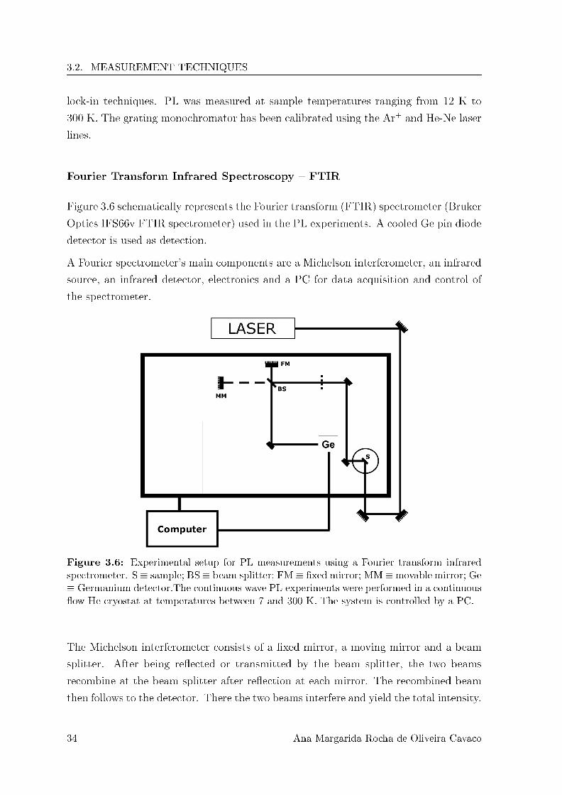

CHAPTER 3. SAMPLE GROWTH AND MEASUREMENT TECHNIQUES
For different positions of the movable mirror, the two partial waves get different phase
shifts with respect to each other. Therefore, on the detector the radiation field is
superimposed with a time-delayed copy of itself. Hence, what is basically measured
when the detector signal is recorded while the mirror moves is the autocorrelation
function of the radiation field (which is called the interferogram in FTIR spectroscopy).
The Fourier transform of this autocorrelation function is the desired power spectrum
in the frequency domain.
If the moving mirror is at the same optical distance from the beam splitter as the fixed
mirror, a constructive interference takes place in the recombined beam, because the
path difference is zero for all wavelengths. But if the moving mirror is displaced by a
distance D, the two beams cover different distances, and the intensity of the interfered
beam changes. The phase difference depends on the displacement of the mirror, D, as
Φ =2πD
λ= 2πkD (3.2)
where k = 1λis the wavenumber.
Assuming the transmission coefficient of the beam splitter to be 50 %, the detected
intensity on the detector for a wavenumber k is:
I = 0.5I0(1 + cos(2πkD)) (3.3)
The detector signal hence represents the interference signal of the two beams coming
from the fixed and the moving mirrors and is therefore dependent on the position of
the moving mirror. If the input beam is not monochromatic, but a spectrum with a
spectral density S(k) — which is, for a FTIR spectrometer, in the IR region — the
detected intensity is
I(D) = 0.5
∫
S(k)[1 + cos(2πkD)]dk. (3.4)
After eliminating the constant part of the signal which is independent of D, the source
spectrum can be obtained by an inverse Fourier transformation
S(k) = 2
∫
I(D) cos(2πkD)dD. (3.5)
The rapid scan function mode of the FTIR spectrometer was used during this work. In
Radiation-Induced Defects in Quantum-Size Structures of A3B5 Semiconductors 35

3.2. MEASUREMENT TECHNIQUES
the rapid scan mode, the mirror rapidly oscillates between the limits. The sampling of
all points is done during one pass of the mirror meaning that the measuring time at each
point is quite short and there is much noise in the spectrum. To obtain a better signal-
to-noise ratio, a mean spectrum of multiple spectra is a result of, say, one hundred
accumulations. The rapid scan mode is used for standard spectroscopy because of the
following reasons: (i) the reduction of the dynamical range of the interferogram with
electrical filters before the analogue-digital conversion, (ii) elimination of low frequency
noise (source fluctuations, electronic and detector deviations, mechanical vibrations,
etc.), and (iii) faster measurements.
The spectral resolution in FTIR is determined by the inverse of the total path of the
movable mirror. In the FTIR spectrometer the calibration of the wavelength scale is
done automatically through the internal He-Ne laser.
The use of a Fourier spectrometer has two main advantages [Bauer and Richter, 1996]:
the multiplex advantage that results from the fact that the light coming from all spec-
tral intervals contributes to the detector signal; and the throughput advantage, since
no slit is necessary, large apertures can be realized resulting in a large throughput.
These features reduce considerably the time needed to record a spectrum.
Resonant Excitation
The experiments under resonant excitation were performed using the setup of figure
3.5. The resonant excitation was possible using a tuneable Ti:Sapphire laser (λ = 850–
1000 nm, Spectra Physics 3900S) which is pumped with an Ar+ laser (Spectra Physics,
model 2085, multiline, CW). PL was measured at sample temperatures ranging from
12 to 300 K. Figure 3.7 presents a diagram illustrating the photon energy ranges of the
sources available for resonant excitation.
3.2.2 Photoluminescence excitation spectroscopy
PLE is a powerful tool for the characterization of an inhomogeneous QD ensemble giv-
ing access to the shape non-uniformity of the islands, the carrier relaxation processes,
and non-radiative recombination. Each single PL spectrum compares QDs with dif-
ferent ground state transition energies, whereas in PLE a subset of the QD ensemble
defined by the ground state transition energy is probed.
Through the choice of a subset of QDs with one and the same ground state energy
36 Ana Margarida Rocha de Oliveira Cavaco

CHAPTER 3. SAMPLE GROWTH AND MEASUREMENT TECHNIQUES
Figure 3.7: Diagram illustrating the photon energy (wavelength) ranges of the sourcesavailable for resonant excitation. The diagram includes sources available in Aveiro and Berlinat the time of the development of the experimental studies. The Ti:Sappire laser in Aveiro wasused as a resonant excitation source in PL experiments, and the OPO in Berlin was used as aresonant excitation source for the TRPL experiments. The above-bandgap excitation TRPLexperiments were performed with the Ti:Sapphire laser from Berlin. The figure includes alsothe emission energies of some of the samples in study. The Ar+ laser is not included since itonly allowed above-bandgap excitation.
from a heterogeneous QD distribution, an improvement of the energy resolution in the
investigation of the excited states is possible, as compared to the usual PL spectroscopy
with above-bandgap excitation.
On the contrary to the PL spectroscopy, where the excitation energy is kept constant
and the spectrum is recorded as a function of the detection energy, in the PLE spec-
troscopy the detection energy is kept constant and the excitation energy is varied. To
ensure a PLE measurement, one has to fulfil three conditions: 1) the excitation light
must be absorbed, 2) the produced electron-hole pairs (excitons) must relax into the
ground state of the QD and 3) the excitons in the QD ground state must undergo
radiative recombination. The main factor affecting the emission intensity in the PLE
Radiation-Induced Defects in Quantum-Size Structures of A3B5 Semiconductors 37

3.2. MEASUREMENT TECHNIQUES
experiments is the efficiency of the light absorption that in turn strongly depends on
the density of states. That is why the absorption is strongest in the bulk matrix, typi-
cally an order of magnitude weaker in the WL and another order of magnitude weaker
in the QDs. This technique offers advantages since it allows resonant excitation at
important PL features such as QD or QW peaks.
Along with the excited states, also phonon-assisted processes can contribute to the
PLE spectra. Therefore we usually observed in the PLE spectra of our InAs/GaAs QD
samples a peak 36 meV above the detection energy caused by the LO-phonon assisted
light absorption in the ground state.
Is there another non-radiative relaxation process, e.g. through the defect levels, also
multi-phonon peaks can be observed [Heitz et al., 1997; Steer et al., 1996] as it occurs
in our irradiated samples.
Figure 3.8: Schematic representation of the setup used, at the Institute of Solid StatePhysics of the Technical University of Berlin, for the PLE experiments. Cr ≡ cryostat andsample; Ch ≡ chopper; Gf = neutral density filter. The neutral density filter is used for anenhancement of the dynamical range of the system.
The PLE experiments were performed in a continuous flow He cryostat between 7 and
300 K. A tungsten lamp dispersed by a 0.27 m double-grating monochromator (Acton
Research 275i) served as a low density, tunable light source. To suppress the stray
light, a double monochromator (Acton Research 300i) was used for the detection of
the emitted light combined with a nitrogen cooled Ge pin diode detector (North Coast,
spectral range 800-1700 nm). In order to enhance the signal-to-noise ratio, a lock-in
38 Ana Margarida Rocha de Oliveira Cavaco

CHAPTER 3. SAMPLE GROWTH AND MEASUREMENT TECHNIQUES
amplifier (Stanford Research 830) was used. The spectrometer has been controlled by
a PC (figure 3.8).
PLE contour plots were also acquired using this setup. In a PLE contour plot, both
excitation and detection energy are varied. For every detection energy value, the
excitation energy is varied from the detection energy to beyond the GaAs bandgap
energy.
3.2.3 Time-resolved photoluminescence
The TRPL allows the determination of the recombination and relaxation times through
the choice of the excitation and detection energies. The dynamical properties of the
systems under investigation can be analysed.
In the present work, the TRPL detection was realized through the single photon count-
ing technique. The scheme of the corresponding facility is represented in figure 3.9. In
this arrangement, a standard PL facility is completed by a reference arm with a trigger
diode and a rapid detector (Multi-channel plate, MCP). As a dispersion element, a sub-
tractive grating spectrometer was used because it does not reduce the time resolution
of the system. Thus, the PL dynamics could be combined with spectral selectivity.
Figure 3.9: Photon counting system. Schematic representation of the setup used at the In-stitute of Solid State Physics of the Technical University of Berlin for the TRPL experiments.A part of the excitation laser beam is directed to the trigger diode (Tr). The laser pulsesinduce a resistance change of the biased diode that are transformed into voltage pulses andyield a fixed reference time for the excitation of the sample. The laser excites the sample inthe cryostat (Cr), and the emitted PL is spectrally dispersed by the monochromators (Mc)and guided to the detector. The MCP (Multi-channel plate) detector transforms the incidentphotons into current pulses that are in turn transformed into voltage pulses by an amplifier.The registered pairs of pulses are combined to yield the time response of the observed PL.
Radiation-Induced Defects in Quantum-Size Structures of A3B5 Semiconductors 39

3.2. MEASUREMENT TECHNIQUES
The excitation was performed by a Ti:Saphire laser and an Optical Parametric Oscil-
lator (OPO) (see figure 3.10). The system functions at a fixed frequency of 80 MHz.
As a pumping laser an Ar+ laser (450-514 nm, < 16 W, CW) has been used. The
Ti:Saphire laser (715-850 nm, < 4 W, CW and 80 MHz, < 50 fs to ≈ 2 ps pulses)
could be used directly as an excitation source or as a pump laser for the OPO. For the
available excitation energy (wavelength) range, see figure 3.7.
Figure 3.10: The infrared laser system. The Ar+ laser (multiline, 450-514 nm) continuouslypumps the Ti:Sapphire laser (690-1000 nm). The latter can oscillate in the CW or pulsed(ps or fs) regime. Because of the different pulse energies in the ps and fs regimes as well asthe necessary spectral compensation in the latter, there are two different OPO systems. Thesystem with the higher requirements to the pumping intensity and beam quality is placed ina way that the beam must not be redirected. For wavelengths below 1130 nm the time driftof the autocorrelation of the OPO could be monitored.
Before striking the sample, the laser beam is divided, thus producing a reference pulse
and an excitation pulse that are time correlated. The reference pulse is transformed
through the trigger diode in an electrical pulse and serves as a time reference. The
PL signal is dispersed by a subtractive double-grating monochromator and detected
by the MCP and appears as an electrical pulse per optical event. The time calibration
of the facility was performed through the detection of the excitation laser. The pulse
full width at half maximum (FWHM) of the latter was 1–3 ps, i.e. much shorter
than the response time of the signal electronics (≈ 18 ps). The time resolution of the
detecting system was about 30 ps. The averaged excitation density within the pulse
was 250 W/cm2.
The samples have been mounted in a bath cryostat at 2 K in superfluid helium in order
to ensure an efficient cooling under intense excitation and reduce the bubble noise.
The TRPL spectra have been evaluated using a fitting procedure based on the expo-
40 Ana Margarida Rocha de Oliveira Cavaco

CHAPTER 3. SAMPLE GROWTH AND MEASUREMENT TECHNIQUES
nential dynamics of a two-level system. The system response measured using excitation
laser pulses served as a starting point for the fitting. As several transitions can con-
tribute to the observed PL signal at a given wavelength, up to four amplitudes with
corresponding time constants have been considered in the fittings. The calculated re-
sult has been fitted to the experimental one through successive iterations. The basic
formula used for calculations was
I(t) =
∫
{L(t− µ, s) + B2} ·n∑
i=1
Aie(−µ/τ)dµ+B1 (3.6)
Here, I(t) is the total amplitude at the time t. Ai and τi are the amplitudes and the time
constants of different two-level systems contributing to the signal and L a correlation
function. Some additional corrections are necessary. The used detector yields a timely
uncorrelated background signal. The latter was determined separately and considered
through the constant B1 (equation (3.6)). The contribution of the background to the
measurement of the system response was considered through the constant B2 (equation
(3.6)). The measurements of the system response and PL were performed at different
detection energies and variable intensities. As the light velocity in air and glass is
subjected to a dispersion, a time shift of the t=0 points occurs when different lenses
and filters are used. This shift is accounted for through the variable s (equation (3.6)).
The fitting was performed using the commercial software “Fluofit”.
3.3 Resume
Experimental setups and growth mechanisms and techniques were briefly reviewed
in this chapter. Growth methods and conditions were also reported. The Stranski-
Krastanow growth mode and the Metal-Organic Chemical Vapour Deposition were
the techniques presented. Several experimental methods were used to characterize the
samples under study. The techniques employed and discussed in this chapter were:
photoluminescence with above-bandgap and resonant excitation, photoluminescence
excitation and time-resolved photoluminescence spectroscopy.
Radiation-Induced Defects in Quantum-Size Structures of A3B5 Semiconductors 41

BIBLIOGRAPHY
Bibliography
Bauer, G. and Richter, W., editors (1996). Optical Characterization of Epitaxial Semi-
conductor Layers. Springer Verlag.
Bimberg, D. (2001). In Proceedings of the 28th International Symposium on Compound
Semiconductors, page 485, Tokyo, Japan.
Bimberg, D., Grundmann, M., and Ledentsov, N. (1999). Quantum Dot Hetero-
structures. John Wiley & Sons, Chichester.
Dutta, M. and Pamulapati, J. (1993). Properties of lattice – matched and strained
Indium Gallium Arsenide, page 199. inspec.
Gerard, J.-M. (1992). Applied Physics Letters, 61:2096.
Goldstein, L., Glas, F., Marzin, J., Charasse, M., and Le Roux, G. (1985). Applied
Physics Letters, 47:1099.
Heinrichsdorff, F., Grundmann, M., Stier, O., Krost, A., and Bimberg, D. (1998a).
Journal of Crystal Growth, 195:540.
Heinrichsdorff, F., Krost, A., Bimberg, D., Kosogov, A., and Werner, P. (1998b).
Applied Surface Science, 123/124:725 – 728.
Heinrichsdorff, F., Krost, A., Grundmann, M., Bimberg, D., Bertram, F., Christen, J.,
Kosogov, A., and Werner, P. (1997). Journal of Crystal Growth, 170:568.
Heinrichsdorff, F., Krost, A., Grundmann, M., Bimberg, D., Kosogov, A., and Werner,
P. (1996). Applied Physics Letters, 68:3284.
Heitz, R., Veith, M., Ledentsov, N., Hoffmann, A., Bimberg, D., Ustinov, M., Kop’ev,
P., and Alferov, Z. (1997). Physical Review B, 56:10435.
Joyce, P., Krzyzewski, T., Bell, G., Jones, T., Le Ru, E., and Murray, R. (2001).
Physical Review B, 64:235317.
Karpovich, I., Zvonkov, B., Baidus, N., Tikhov, S., and Filatov, D. (2004). Trends in
Nanotechnology Research, chapter Tunning the energy spectrum of the InAs/GaAs
Quantum dot structures by varying the thickness and composition of a thin double
GaAs/InGaAs cladding layer, page 173. Nova Science, New York.
42 Ana Margarida Rocha de Oliveira Cavaco

CHAPTER 3. SAMPLE GROWTH AND MEASUREMENT TECHNIQUES
Ledentsov, N., Bimberg, D., Ustinov, V., Alferov, Z., and Lott, J. (2002). Japanese
Journal of Applied Physics, 41:949.
Leon, R., Lobo, C., Liao, X., Zou, J., Cockayne, D., and Fafard, S. (1999). Thin Solid
Films, 357:40.
Pereira, S. (2005). private communication.
Reithmaier, J.-P., Riechert, H., Schlotterer, H., and Weimann, G. (1991). Journal of
Crystal Growth, 111:407.
Sellin, R. (2003). Metalorganic Chemical Vapor Deposition of High-Performance GaAs-
Based Quantum-Dot Lasers. PhD thesis, von der Fakultat II – Mathematik und
Naturwissenschaften – der Technischen Universitat Berlin, Berlin.
Steer, M., Mowbray, D., Tribe, W., Skolnick, M., Sturge, M., Hopkinson, M., Cullis,
A., Whitehouse, C., and Murray, R. (1996). Physical Review B, 54:17738.
Stringfellow, G. (1999). Organometallic Vapor-Phase Epitaxy. Academic Press, 2nd
edition.
Toyoshima, H., Niwa, T., Yamazaki, J., and Okamoto, A. (1993). Applied Physics
Letters, 63:821.
Wang, S., Andersson, T., and Ekenstedt, M. (1991). Applied Physics Letters, 59:2156.
Wikipedia (2010). Stranski-krastanow growth. http://en.wikipedia.org/wiki/
Stranski-Krastanov-growth.
Zvonkov, B., Karpovich, I., Baidus, N., Filatov, D., Morozov, S., and Gushina, Y.
(2000). Nanotechnology, 11.
Radiation-Induced Defects in Quantum-Size Structures of A3B5 Semiconductors 43

BIBLIOGRAPHY
44 Ana Margarida Rocha de Oliveira Cavaco


4.1. LASER STRUCTURES
in laser structures [Heinrichsdorff et al., 1997b]. The structure was grown on top of a
GaAs substrate and a GaAs buffer layer. TEM results on similar samples give typical
QD densities of 5×1010 cm−2 [Heinrichsdorff et al., 1998b, 1997b,c].
Figure 4.2: FTIR PL spectra of as-grown (before irradiation) samples 1×QD, CQW and5×QD measured at 10 K upon excitation with the 457.9 nm line of an Ar+ laser. The PLintensity is normalized to the excitation power. The latter did not exceed ≈ 102 W/cm2 toavoid PL and detector saturation.
Upon excitation above the GaAs bandgap (1.5192 eV at T = 2 K [Madelung, 1987])
with the 457.9 nm (2.7 eV) line of an Ar+ laser, strong QW and QD PL bands emerge
due to exciton transitions involving electrons and holes in the ground state (figure 4.2).
The QD emissions lead, for samples 5×QD and 1×QD, to peaks at 1.214 and 1.232 eV
with FWHMs of 55 and 65 meV, respectively. Sample CQW exhibits a PL emission
at 1.345 eV with a FWHM of 12 meV (figure 4.2). The QD PL peaks are of Gaussian
shape (see fittings in figure 4.3).
The growth of several layers of QDs allows a significant increase of the total number
of QDs, giving rise to an enhancement of the QD PL intensity, as shown in figure 4.2
for sample 5×QD. The barrier thickness determines the degree of vertical alignment
and electronic coupling. Sample 5×QD has 20 nm thick GaAs barriers between layers
of QDs. For this thickness the alignment is already lost, as shown by TEM results in
similar samples [Heinrichsdorff et al., 1997b; Xie et al., 1995].
No PL due to excited states or WL could be seen at low excitation densities, indicating
rapid carrier transfer from the WL to the QDs and high density of dots. A slightly larger
46 Ana Margarida Rocha de Oliveira Cavaco

CHAPTER 4. CHARACTERIZATION OF THE AS-GROWN SAMPLES
Figure 4.3: PL spectra of samples 1×QD (left) and 5×QD (right), both as-grown, showingthe fit used to determine the peak position and FWHM. A Gaussian function was used toperform the fit.
average InAs island size in sample 5×QD as compared to sample 1×QD can be inferred
from the peak energy position, as well as a higher homogeneity of the dots from the
FWHM. Each QD has its particular set of energy levels. The distribution of these levels
among the QD ensemble gives rise to different values of FWHM. For larger ensembles of
QDs, the inhomogeneous line broadening may be due to fluctuations of size, shape, and
chemical composition [Bimberg et al., 1999]. The shape of the QDs is the main factor
governing the strain distribution, not the size [Grundmann et al., 1995]. Theoretical
calculations performed using effective mass approximation [Grundmann et al., 1995]
and eight-band k·p theory [Stier et al., 1999] predict for the observed QD ground
state energies (figure 4.2) pyramid base lengths of 9 and 10 nm, respectively. The
different base length values are related to different band offsets used in the calculations.
According to the latter, it was not possible to establish different pyramid base length
for the samples under study due to the small difference between the peak energies.
An important note is that both calculations were performed for pyramid shape QDs
and not for truncated pyramids. The luminescence efficiency obtained from these QD
arrays is similar to that of the QW sample. The predicted primary consequence of a
phonon bottleneck, completely quenched luminescence efficiency [Benisty et al., 1991]
is not observed. As proposed in many different works, several relaxation mechanisms
can provide the non-existence of this phonon bottleneck (see discussion of the carrier
dynamics in section 6.2).
Figure 4.4 shows the temperature dependence of the integrated PL intensity (top),
FWHM (middle) and peak position (bottom) of the QD or QW emission, according to
the sample. For the QD samples, the FWHM goes to a minimum value at a temper-
ature of ≈150 K in agreement with other works on similar samples [Lubyshev et al.,
Radiation-Induced Defects in Quantum-Size Structures of A3B5 Semiconductors 47

4.1. LASER STRUCTURES
Figure 4.4: Temperature dependence, between 10 and 300 K, of the PL characteristicsfor the as-grown samples 1×QD, CQW and 5×QD. Top: integrated PL intensity, middle:full width at half maximum (FWHM), and bottom: QD or QW band peak position. Forcomparison the variation of the InAs bandgap (+0.82 eV), calculated using Varshni’s lawwith the InAs parameters [Varshni, 1967], is shown as a blue line in the bottom graph of thefigure.
48 Ana Margarida Rocha de Oliveira Cavaco

CHAPTER 4. CHARACTERIZATION OF THE AS-GROWN SAMPLES
1996; Patane et al., 1997; Xu et al., 1998]. Assuming a uniform energy barrier of the
wetting layer, the thermal activation energy differs from dot to dot due to the size
distribution. As the temperature increases, excitons at shallow potential minima can
easily be thermally activated out to the energy barrier produced by the wetting layer,
and then recombine radiatively or non-radiatively there, and/or transfer and relax into
energetically low-lying states. Consequently, high energy components in the PL spec-
trum shrink much faster than the low energy components, resulting in the fast red shift
of the PL peak energy, faster than for the InAs energy gap (see figure 4.4 bottom), and
reduction of the FWHM (figure 4.4 middle). The carrier redistribution between dots
is also evident from the temperature dependence of the integrated PL intensity (figure
4.4 top). As the PL line width (FWHM) shrinks, the integrated PL intensity reaches
a maximum due to carriers feeding into the lower energy dots from the higher energy
ones. This redistribution of carriers between dots can also explain the behaviour of
the QD band position with temperature as referred before. If this redistribution pro-
cess would be absent, the QD PL peak position would follow the band-gap thermal
shrinkage for all temperatures, as has been seen in the temperature dependence of the
absorption-like spectra [Aigouy et al., 1997].
The exponentially decreasing temperature dependence of the QD PL intensity observed
for samples TU3904 and TU3972 is quite common and has been modelled in several
publications [Altieri et al., 2002; Brusaferri et al., 1996; Chang et al., 2005; Le Ru et al.,
2003; Lee et al., 2008; Wasilewski et al., 1999; Wei et al., 2005]. The main problem is
that for similar samples, quite different results have been found. For a discussion of the
influence of defects on the temperature dependence of the PL intensity see chapter 7.
4.2 Samples with non-uniform WL thickness
Some samples studied in this thesis had a non-uniform WL thickness. In these samples
the WL assumes a complex structure containing growth islands. The latter have dif-
ferent thicknesses, going from 5 to 9 ML. The occurrence of this monolayer splitting of
the WL is dependent on the substrate temperature during the growth [Heinrichsdorff
et al., 1996]. These samples were used to gain additional insight into the influence of
the WL thickness on the thermal carrier/exciton redistribution within the QDs.
The samples used were grown by MOCVD and have the following structure (figure
4.5): a GaAs buffer layer was grown on top of a GaAs:Te substrate, the active layer
Radiation-Induced Defects in Quantum-Size Structures of A3B5 Semiconductors 49

4.2. SAMPLES WITH NON-UNIFORM WL THICKNESS
(a) TU3581 (b) TU4736 (c) TU4738 (d) TU5330
Figure 4.5: Layer sequence of the samples with non-uniform WL thickness. The activelayers are composed of In0.6Ga0.4As QDs grown at temperatures between 490 and 525 �.Layer thicknesses and compositions are indicated in the diagrams.
together with GaAs cladding layers were placed between two AlGaAs barriers, with a
GaAs capping layer on top of the whole structure. After the active layer growth, an
interruption between 4.6 and 16.6 s was performed in order to allow the QDs to grow
[Heinrichsdorff et al., 1997a].
Sample TU3581 has a low density of QDs, less then the other samples of this group,
with large-size QDs. In the TEM image (figure 4.6), two classes of three-dimensional
objects can be distinguished. Besides the QDs, large clusters can be observed with no
uniform shape and which size is far beyond the critical size for dislocation generation.
Thus, the strain is relieved by plastic relaxation and a minimization of strain energy
plays no role for these clusters.
Samples TU4736 and TU5330 have a dot density of ≈109 cm−2 and sample TU4738
has a dot density < 109 cm−2, all samples with an active layer composed by a single
QD layer.
Figures 4.7, 4.8 and 4.9 show PL spectra of the as-grown sample TU5330 taken at
10, 70, and 300 K, respectively. The spectra were obtained at a FTIR spectrometer
with the 457.9 nm line of an Ar+ laser as excitation source and detected by a liquid-
nitrogen cooled Ge detector. The sample was mounted in a He flux cryostat that allows
measurements in the temperature range from 10 to 300 K. In each spectrum, QD and
WL emission energies are identified. The energy peaks were determined using Gaussian
50 Ana Margarida Rocha de Oliveira Cavaco

CHAPTER 4. CHARACTERIZATION OF THE AS-GROWN SAMPLES
Figure 4.6: Plan view TEM image of sample TU3581.
fit functions (green curves in the figures) for each emission.
At 10 K, the luminescence of the QD ensemble appears as a double-peaked band
centred between 1.1 and 1.2 eV. The low-energy peak at 1.120 eV with a FWHM of
46 meV corresponds to the ground state transition; the peak at 1.179 eV originates
from excited states and is visible due to state filling effects favoured by the low QD
density [Grundmann et al., 1996] and the slowed down relaxation from the first excited
to the ground state, as will be discussed in section 6.4.1. For lower excitation densities,
the peak at 1.179 eV is absent. The more dominant feature of the spectrum is a multi-
peaked band with the individual maxima centred between 1.238 and 1.362 eV which
stem from the WL. Beside the two main peaks at 1.306 and 1.338 eV, three additional
peaks can be observed. All these peaks are attributed to a monolayer (ML)-sized
splitting of the WL.
At 70 K, the same structure of bands is observed (figure 4.8), though here the resolution
is worse than at 10 K. At 300 K, another QD-related band arises which is attributed
to the second excited state (figure 4.9). The QD emission is now stronger than the WL
emission. This is so due to the lower localization energy for the carriers in the WL and
to the higher thermal excitation energy available at room temperature.
Similar results were observed for other samples (see an example in figure 4.10). Figure
4.10a shows PL spectra of sample TU4738 taken at different temperatures indicated in
Radiation-Induced Defects in Quantum-Size Structures of A3B5 Semiconductors 51

4.2. SAMPLES WITH NON-UNIFORM WL THICKNESS
Figure 4.7: PL spectrum of the as-grown sample TU5330 taken at 10 K.
Figure 4.8: PL spectrum of the as-grown sample TU5330 taken at 70 K.
52 Ana Margarida Rocha de Oliveira Cavaco

CHAPTER 4. CHARACTERIZATION OF THE AS-GROWN SAMPLES
Figure 4.9: PL spectrum of the as-grown sample TU5330 taken at 300 K.
the figure. The curves are vertically shifted for clarity. The WL PL emission quenching
is visible and only one rather broad band remains at 300 K. At 70 K (figure 4.10b) one
emission band from QDs and four emission bands from the WL can be identified.
Samples TU4738 and TU4736 are very similar. The main difference is the dot density
which can be corroborated by the intensity of the QD PL band, since TU4736 has a
higher density and hence a higher relative QD PL intensity (figure 4.11).
Sample TU3581 has the largest QD size which can be inferred from the lowest QD
peak energy, around 0.95 eV at 300 K.
Figure 4.12a shows PL and PLE spectra of the as-grown sample TU5330 taken at
7 K. The PL spectrum was obtained with above-GaAs bandgap excitation. The PLE
spectrum was detected at the QD PL maximum. In this spectrum a GaAs LO-phonon
emission can be observed. From this spectrum it can be concluded that the QD ground
state is fed with carriers from the GaAs barrier, the WL and the QD excited states.
Figure 4.12b shows a PLE contour plot of the same sample. For the as-grown sample no
resonance at the QD first excited state can be observed. For a more detailed discussion
of these results see section 6.4.
To study in more detail the emissions attributed to the WL, PL spectra were taken
at temperatures between 10 K and room temperature. The temperature dependence
of the integrated intensities of the different PL peaks is displayed in figure 4.13. The
Radiation-Induced Defects in Quantum-Size Structures of A3B5 Semiconductors 53

4.2. SAMPLES WITH NON-UNIFORM WL THICKNESS
Figure 4.10: (a) PL spectra of the as-grown sample TU4738 taken at different temperaturesas indicated in the figure. Note the logarithmic intensity scale. The curves are verticallyshifted for clarity. (b) PL spectrum of the same sample taken at 70 K with indication of thepeak positions for the QD ground state- and WL-related emissions.
54 Ana Margarida Rocha de Oliveira Cavaco

CHAPTER 4. CHARACTERIZATION OF THE AS-GROWN SAMPLES
Figure 4.11: PL spectra of different as-grown samples taken at 10 K. The vertical linesindicate the WL peak positions for 5, 6, 7, 8, and 9 ML thick WL islands determined for thesample TU5330.
Radiation-Induced Defects in Quantum-Size Structures of A3B5 Semiconductors 55

4.2. SAMPLES WITH NON-UNIFORM WL THICKNESS
Figure 4.12: (a) PL and PLE spectra of the as-grown sample TU5330 taken at 7 K.QD-, WL- and GaAs-related emission bands are identified. (b) Contour plot of the QD PLintensity measured at 7 K as a function of the detection and the excitation energy for the as-grown sample TU5330. The white line denotes the position of the QD ground state emissionmaximum.
56 Ana Margarida Rocha de Oliveira Cavaco

CHAPTER 4. CHARACTERIZATION OF THE AS-GROWN SAMPLES
Figure 4.13: Temperature dependence of the integrated PL intensity for different identifiedQD and WL emissions for the as-grown sample TU5330. For peak positions at 10 K see figure4.7. The intensities were all normalized to the 10 K value.
intensity of the luminescence of the 5 and 6 ML WL parts drops continuously with
rising temperature. The intensities related to the 7, 8 and 9 ML thick WL regions rise
with increasing temperature up to a certain point and then drop quite quickly. The
temperature at which the luminescence intensity reaches its maximum is the higher the
thicker the WL region is. It is a manifestation of the Maxwell-Boltzmann distribution
of excitons over WL parts of different thickness and, consequently, different well depths.
With increasing temperature the peaks attributed to the thicker parts of the WL gain
luminescence intensity (figure 4.13) at the expense of the peaks of the thinner parts.
Above 150 K the luminescence of the WL peaks disappears completely. The intensity
of the QD peak rises continuously with increasing temperature until 260 K, starting to
decrease after that.
4.3 TU5411: dots-in-a-well structure
Sample TU5411 was grown using MOCVD and has the structure seen in figure 4.14.
After the 200 nm GaAs buffer layer grown on top of a GaAs substrate, an AlGaAs
barrier followed by 100 nm GaAs were grown at 600 �. Subsequently, the temperature
was lowered to 485 � for the deposition of ≈2.1 monolayers (ML) of InAs forming
Radiation-Induced Defects in Quantum-Size Structures of A3B5 Semiconductors 57

4.3. TU5411: DOTS-IN-A-WELL STRUCTURE
the initial InAs islands. The islands were capped by a 2 nm thick In0.25Ga0.75As layer.
Finally, the temperature was raised to 600� for the growth of 50 nm GaAs, an AlGaAs
barrier and a 20 nm GaAs protection layer. The lateral density of the QDs determined
from plane-view TEM images was ≈(3–5)×1010 cm−2. The InAs QDs are embedded
in a QW formed by the original InAs WL and the In0.25Ga0.75As cap layer. For the
investigated samples TEM results suggest a flat truncated shape of the overgrown InAs
QDs with a base length between 12 nm and 14 nm and an estimated height around
3 nm.
Figure 4.14: Layer sequence of the sample TU5411.
The high QD density does not allow the observation of PL bands related to excited
states in a low excitation regime. Figure 4.15 shows a FTIR PL spectrum of sample
TU5411 taken at 10 K upon excitation with the 488 nm line of an Ar+ laser. A single
QD band is observed at 1.04 eV. The other energy positions identified, E = 1.12 eV and
E = 1.14 eV, are assigned to sub-levels of the first excited state which have been inves-
tigated in the TRPL experiments described in section 6.4. This sample was measured
at TU Berlin by Dr. Roman Sellin in the high excitation regime, using an excitation
power of 500 mW, at room temperature, and two excited states and a WL band could
be identified (figure 4.16). The emission around 1.4 eV is GaAs-related.
Figure 4.17 shows PL and PLE spectra of the as-grown sample TU5411 taken at 7 K.
The PL spectrum was obtained with above-bandgap excitation. A band originating at
the QD ground state and the GaAs barrier-related emission can be identified in this
spectrum. The PLE spectrum was detected at the QD PL maximum position. It shows
LO-phonon-assisted ground state absorption at 1.08 eV, two bands arising from the
first and second excited QD states and a WL/QW-related band around 1.3 eV.
58 Ana Margarida Rocha de Oliveira Cavaco

CHAPTER 4. CHARACTERIZATION OF THE AS-GROWN SAMPLES
Figure 4.15: FTIR PL spectrum of the as-grown sample TU5411 taken at 10 K uponexcitation with the 488 nm line of an Ar+ laser.
Figure 4.16: PL spectrum of the as-grown sample TU5411 taken at 300 K with an excitationpower of 500 mW. This spectrum was obtained at TU Berlin and kindly made available byDr. Roman Sellin.
Radiation-Induced Defects in Quantum-Size Structures of A3B5 Semiconductors 59

4.4. OTHER DOTS-IN-A-WELL STRUCTURES WITH DIFFERENT CAP LAYER
THICKNESSES
Figure 4.17: PL and PLE spectra of the as-grown sample TU5411 taken at 7 K. For the PLEspectrum the detection energy was set at the QD PL maximum position. The PL spectrumwas obtained with above-bandgap excitation.
4.4 Other dots-in-a-well structures with different
cap layer thicknesses
Table 4.1: Sample characteristics.
Sample dc (nm) L (nm) xNN3649 5 4 0.2NN3652 5 2 0.2NN3653 5 2 0.3NN3654 5 4 0.3NN3753 20 2 0.3NN3756 5 2 0.3NN3760 10 2 0.3NN3761 7 2 0.3NN3762 3 2 0.3
Growing the InAs/GaAs QDs emitting in the optical silica glass fibre transparency
windows at 1.3 (0.9 eV) and 1.55 µm (0.8 eV) still remains an important technological
problem. One of the approaches to this problem is growth of an InxGa1−xAs quantum
well over the QDs, which results in a red shift of the QD ground state [Kovsh et al.,
60 Ana Margarida Rocha de Oliveira Cavaco

CHAPTER 4. CHARACTERIZATION OF THE AS-GROWN SAMPLES
1999; Nishi et al., 1999; Volovik et al., 1999]. The samples studied differed in thickness
and In content of the QW overgrowing the dots as well as the thickness of the capping
layer. This study allowed a better understanding of the influence of the parameters
referred before on the energy spectrum of the QDs.
The samples used in this study were grown at Nizhny Novgorod University by atmo-
spheric pressure metal organic vapour phase epitaxy (AP-MOVPE). On top of the
GaAs substrate, a 600 nm GaAs buffer layer was grown. Then the deposition of InAs
began in order to form a wetting layer and the QDs layer. An InGaAs layer was grown
on top of the QDs, placed between the QDs layer and the GaAs cap layer (see fig-
ure 4.18). Differences between samples (see figure 4.18 and table 4.1) are related to
variations of the QW thickness (L), QW indium content (x) and GaAs caping layer
thickness (dc).
Figure 4.18: Layer sequence of the samples with different cap layer thicknesses. Samplesare labelled after table 4.1, where dc is the cap layer thickness, L is the InxGa1−xAs QWthickness and x is the In content in the QW.
As expected, decreasing the GaAs cap layer thickness results in a red shift of the ground
state transition energy (figures 4.19 and 4.20) due to increased compressive strain, but
the emission intensity from the capped QDs is enhanced as fewer carriers undergo non-
radiative recombination at surface states [Saito et al., 1998]. No emission from the
WL or the QW was observed at room temperature for any of the samples under study.
At low temperature (4.4 K), in the PL spectrum of sample NN3753 (dc = 20 nm) an
emission band around 1.3 eV can be observed (see figure 4.23) that can be attributed
to the QW/WL.
The decrease of the cap layer thickness from 20 to 3 nm results in a decrease of the
Radiation-Induced Defects in Quantum-Size Structures of A3B5 Semiconductors 61

4.4. OTHER DOTS-IN-A-WELL STRUCTURES WITH DIFFERENT CAP LAYER
THICKNESSES
Figure 4.19: PL spectra of thin cap layer samples. The cap layer thickness is identifiedin the figure. The spectra were obtained with a 457.9 nm line of an Ar+ laser as excitationsource. Samples with L = 2 nm (InGaAs QW thickness) and x = 0.3 (In content of QW).
QD ground state transition energy from 0.87 to 0.715 eV (figures 4.19 and 4.20). A
shoulder at higher energies can be observed in the PL spectra (figure 4.19), probably
arising from excited QD states but this was not explored. The decrease of the ground
state luminescence (figure 4.19) with decreasing cap layer thickness can be attributed
to an additional non-radiative recombination channel: direct tunnelling of the photo-
excited carriers from the QD ground state to the surface. As the cap layer thickness
decreases, the tunnelling transitions of the electrons from the confined QD levels to the
surface states followed by their non-radiative recombination become possible. AFM
measurements performed in similar samples revealed a typical lateral base size of the
QDs of 40 to 50 nm and height varying from 4 to 6 nm depending on the QDs origin
being a surface layer or an etched one [Karpovich et al., 2001].
The temperature dependence of the QD ground state PL emission of the 10 nm cap layer
sample (NN3760) was investigated and is shown in figure 4.21. The temperature was
varied between 10 and 150 K; above 160 K no luminescence could be seen due to thermal
quenching. The difference in the behaviour of the transition energy with temperature
between samples TU3904 and NN3760 (cf. figures 4.4 and 4.21) is obviously related
to the different energy spacing between the QD and QW/WL ground states which is
62 Ana Margarida Rocha de Oliveira Cavaco

CHAPTER 4. CHARACTERIZATION OF THE AS-GROWN SAMPLES
Figure 4.20: QD ground state transition energy at room temperature vs. GaAs cap layerthickness.
much larger in the latter sample.
The influence of the QW thickness and In content in the QW for samples having the
same GaAs cap layer thickness is shown in figure 4.22. From these results a shift toward
lower energies is observed with the increase of the QW thickness and the increase in In
content in the QW. The QW thickness appears to have a different influence depending
on the In content, showing a higher band shift for the 30% In content.
The QD ground state of these samples seems to be only excited through the GaAs
barrier and the WL as can be seen in the PLE spectra (see figures 4.23, 4.24 and
4.25). Within most of the spectra no fine structure related to excitation via excited
states could be observed. However, sample NN3760 (dc = 10 nm) is an exception. The
PLE spectrum shows two peaks (denoted by red arrows in figure 4.23 top) spaced by
≈70 meV which can arise from QD excited states. The poor signal-to-noise ratio in
these experiments hampered the quantitative evaluation of the emissions.
As a function of temperature the PLE (figure 4.24) spectra show almost no differences
between 4 and 160 K for the samples with 10 and 20 nm of capping layer thickness.
At 200 K, only the 20 nm capping layer sample spectrum is shown since the PL of the
10 nm capping layer sample is already quenched. As stated before, the temperature
Radiation-Induced Defects in Quantum-Size Structures of A3B5 Semiconductors 63

4.4. OTHER DOTS-IN-A-WELL STRUCTURES WITH DIFFERENT CAP LAYER
THICKNESSES
Figure 4.21: Temperature dependence results for sample NN3760 with 10 nm cap layerthickness. Top: QD ground state peak energy position. Middle: integrated PL intensity.Bottom: full width at half maximum (FWHM). For comparison the variation of the InAsbandgap (+0.466 eV), calculated using Varshni’s law with the InAs parameters [Varshni,1967], is shown as a solid line in the top graph of the figure.
64 Ana Margarida Rocha de Oliveira Cavaco

CHAPTER 4. CHARACTERIZATION OF THE AS-GROWN SAMPLES
Figure 4.22: PL spectra of thin cap layer samples with different QW thickness and Incontent in QW, both indicated in the figure. The cap layer thickness is 5 nm. The spectrawere obtained at RT with the 457.9 nm line of an Ar+ laser as excitation source.
increase does not reveal any fine structure arising from excitation via QD states.
Decreasing the In content in the InGaAs QW induces a red shift of the QD ground
state (identified in the PL spectrum, figure 4.25 bottom) and QW emission (identified
in the PLE spectrum, figure 4.25 top).
The changes in the QD energy spectrum were attributed to the variation of the elastic
strain in the pseudomorphic QDs [Karpovich et al., 2004].
Radiation-Induced Defects in Quantum-Size Structures of A3B5 Semiconductors 65

4.4. OTHER DOTS-IN-A-WELL STRUCTURES WITH DIFFERENT CAP LAYER
THICKNESSES
Figure 4.23: PL (black curves) and PLE (red curves) spectra of samples NN3753(d c = 20 nm, bottom graph) and NN3760 (d c = 10 nm, top graph) taken at 4.4 K. Thesamples have L = 2 nm (InGaAs QW thickness) and x = 0.3 (In content in QW). The peaksrelated to the QDs, WL and GaAs band edge emission are clearly seen.
66 Ana Margarida Rocha de Oliveira Cavaco

CHAPTER 4. CHARACTERIZATION OF THE AS-GROWN SAMPLES
Figure 4.24: PLE spectra of samples with different cap layer thicknesses, indicated in thefigure (top: NN3760 – dc = 10 nm and bottom: NN3753 – dc = 20 nm). All sampleshave L = 2 nm (InGaAs QW thickness) and x = 0.3 (In content of QW). The spectra arenormalized to the intensity above the GaAs bandgap. Note the shift of the GaAs bandgapwith temperature.
Radiation-Induced Defects in Quantum-Size Structures of A3B5 Semiconductors 67

4.4. OTHER DOTS-IN-A-WELL STRUCTURES WITH DIFFERENT CAP LAYER
THICKNESSES
Figure 4.25: PLE (upper panel) and PL (lower panel) spectra taken at 4.4 K on sampleswith a cap layer thickness of 5 nm and QW thickness L = 4 nm. The samples have differentIn content in the QW, as indicated in the figure.
68 Ana Margarida Rocha de Oliveira Cavaco
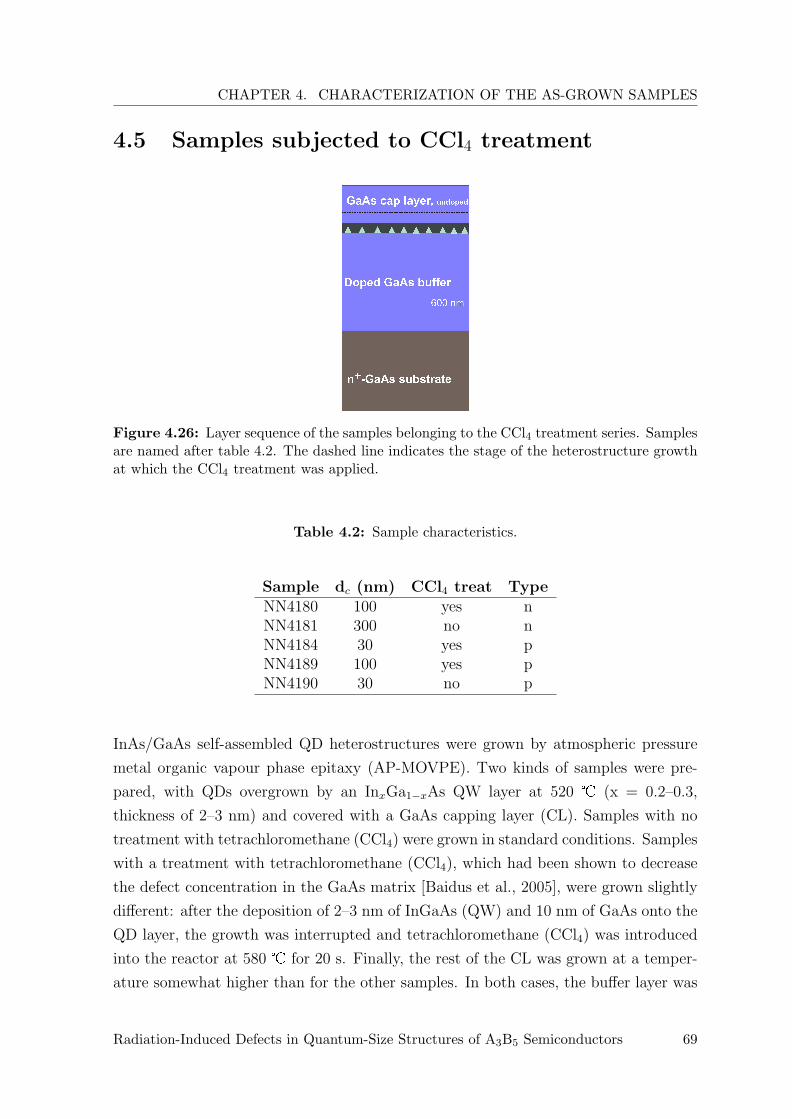
CHAPTER 4. CHARACTERIZATION OF THE AS-GROWN SAMPLES
4.5 Samples subjected to CCl4 treatment
Figure 4.26: Layer sequence of the samples belonging to the CCl4 treatment series. Samplesare named after table 4.2. The dashed line indicates the stage of the heterostructure growthat which the CCl4 treatment was applied.
Table 4.2: Sample characteristics.
Sample dc (nm) CCl4 treat TypeNN4180 100 yes nNN4181 300 no nNN4184 30 yes pNN4189 100 yes pNN4190 30 no p
InAs/GaAs self-assembled QD heterostructures were grown by atmospheric pressure
metal organic vapour phase epitaxy (AP-MOVPE). Two kinds of samples were pre-
pared, with QDs overgrown by an InxGa1−xAs QW layer at 520 � (x = 0.2–0.3,
thickness of 2–3 nm) and covered with a GaAs capping layer (CL). Samples with no
treatment with tetrachloromethane (CCl4) were grown in standard conditions. Samples
with a treatment with tetrachloromethane (CCl4), which had been shown to decrease
the defect concentration in the GaAs matrix [Baidus et al., 2005], were grown slightly
different: after the deposition of 2–3 nm of InGaAs (QW) and 10 nm of GaAs onto the
QD layer, the growth was interrupted and tetrachloromethane (CCl4) was introduced
into the reactor at 580 � for 20 s. Finally, the rest of the CL was grown at a temper-
ature somewhat higher than for the other samples. In both cases, the buffer layer was
Radiation-Induced Defects in Quantum-Size Structures of A3B5 Semiconductors 69

4.5. SAMPLES SUBJECTED TO CCL4 TREATMENT
p-type doped by laser-assisted evaporation of Zn during its growth. This resulted in
an acceptor concentration of 1017 cm−3 in the buffer layer, while the capping layer was
not intentionally doped.
The CCl4 post-growth treatment helps to dissolve the InGaAs clusters as was estab-
lished by means of AFM [Karpovich et al., 2004]. The morphology of the SAQDs
and the roughness of the top surface were explored by AFM. AFM images of uncov-
ered SAQDs, grown under the same conditions, have shown a high size and shape
uniformity [Karpovich et al., 2004]. The (uncovered) dot density was measured to be
1.6×1010 cm−2.
Figure 4.27: PL spectra of samples from the # 41 series taken at 12 K. Sample character-istics and labels are according to table 4.2 and the spectra are all normalized to the incidentpower.
Figure 4.27 shows PL spectra of samples from the # 41 series taken at 12 K. Figure
4.28 shows PL spectra of samples NN4184 and NN4190 taken at 12 K. These samples
are similar differing only in the CCl4 treatment, as indicated in the figure. The QD PL
band shifts to higher energies when submitted to the CCl4 treatment. The increased
temperature used after the CCl4 treatment explains this shift [Heinrichsdorff et al.,
1998a].
The PL intensity temperature dependence is discussed in a dedicated chapter (chap-
ter 7). There more results on these samples and their discussion can be found.
70 Ana Margarida Rocha de Oliveira Cavaco

CHAPTER 4. CHARACTERIZATION OF THE AS-GROWN SAMPLES
Figure 4.28: PL spectra of two similar samples taken at 12 K, showing the influence of theCCl4 treatment on the QD PL emission.
Figure 4.29: Temperature dependence of the QD PL emission from samples of the # 41series. Sample characteristics and labels are according to table 4.2 .
Radiation-Induced Defects in Quantum-Size Structures of A3B5 Semiconductors 71

4.6. CONCLUSIONS
4.6 Conclusions
The characterization of samples prior to irradiation is presented and discussed in this
chapter. Samples with different structures were characterized and the results are pre-
sented here. The chapter includes results obtained on laser structure samples and
samples with non-uniform wetting layer thickness, as well as samples where the influ-
ence of the cap layer thickness and of the treatment with CCl4 on the quantum dot
emission was investigated.
The samples used in this thesis were described and characterized prior to irradiation.
The sample structures were presented and the main growth conditions introduced. The
influence of parameters such as wetting layer and cap layer thickness, treatment with
CCl4 during the growth and In content on the QD and QW PL emission was investi-
gated. The QD and QW PL emission temperature dependence was also presented for
some of the samples.
The study of the laser structures showed that the growth of several layers of QDs allows
a significant enhancement of the QD PL intensity. A process of carrier redistribution
between dots can explain the behaviour of the QD band emission with temperature.
For the sample with non-uniform wetting layer thickness, the PL spectrum shows a
multi-peaked band with the individual maxima centred between 1.238 and 1.362 eV
which stem from the WL. Beside the two main peaks at 1.306 and 1.338 eV, three
additional peaks can be observed. All these peaks are attributed to a monolayer (ML)-
sized splitting of the WL.
The high QD density found in sample TU5411 does not allow the observation of PL
bands related to excited states in the low-excitation regime. However, an efficient
feeding of carriers from the excited states to the ground state could be found in PLE
experiments.
The decrease of the cap layer thickness from 20 to 3 nm results in a decrease of the
QD ground state transition energy from 0.87 to 0.715 eV. The decrease of the ground
state luminescence intensity with decreasing cap layer thickness can be attributed to an
additional non-radiative recombination channel: direct tunnelling of the photo-excited
carriers from the QD ground states to the surface. Decreasing the In content in the
InGaAs QW induces a red shift of the QD ground state
A blue shift of the QD ground state emission was found when the structure was sub-
mitted to the CCl4 treatment.
72 Ana Margarida Rocha de Oliveira Cavaco

CHAPTER 4. CHARACTERIZATION OF THE AS-GROWN SAMPLES
Bibliography
Aigouy, L., Holden, T., Pollak, F., Ledentsov, N., Ustinov, V., Kop’ev, P., and Bimberg,
D. (1997). Applied Physics Letters, 70:3329.
Altieri, P., Gurioli, M., Sanguinetti, S., Grilli, E., Guzzi, M., Fiogeri, P., and Franchi,
S. (2002). The European Physical Journal B, 28:157.
Baidus, N., Chahboun, A., Gomes, M., Vasilevskiy, M., Demina, P., Uskova, E., and
Zvonkov, B. (2005). Applied Physics Letters, 87(5):053109.
Benisty, H., Sotomayor-Torres, C., and Weisbuch, C. (1991). Physical Review B,
44(19):10945.
Bimberg, D., Grundmann, M., and Ledentsov, N. (1999). Quantum Dot Hetero-
structures. John Wiley & Sons, Chichester.
Brusaferri, L., Sanguinetti, S., Grilli, E., Guzzi, M., Bignazzi, A., Bogani, F., Carraresi,
L., Colocci, M., Bosacchi, A., Frigeri, P., and Franchi, S. (1996). Applied Physics
Letters, 69:3354.
Chang, K., Yang, S., Chuu, D., Hsiao, R., Chen, J., Wei, L., Wang, J., and Chi, J.
(2005). Journal of Applied Physics, 97:083511.
Grundmann, M., Ledentsov, N., Stier, O., Bohrer, J., Bimberg, D., Ustinov, V.,
Kop’ev, P., and Alferov, Z. (1996). Physical Review B, 53(16):R10509.
Grundmann, M., Stier, O., and Bimberg, D. (1995). Physical Review B, 52:11969.
Heinrichsdorff, F., Grundmann, M., Stier, O., Krost, A., and Bimberg, D. (1998a).
Journal of Crystal Growth, 195:540.
Heinrichsdorff, F., Krost, A., Bimberg, D., Kosogov, A., and Werner, P. (1998b).
Applied Surface Science, 123/124:725 – 728.
Heinrichsdorff, F., Krost, A., Grundmann, M., Bimberg, D., Bertram, F., Christen, J.,
Kosogov, A., and Werner, P. (1997a). Journal of Crystal Growth, 170:568.
Heinrichsdorff, F., Krost, A., Grundmann, M., Bimberg, D., Kosogov, A., and Werner,
P. (1996). Applied Physics Letters, 68:3284.
Radiation-Induced Defects in Quantum-Size Structures of A3B5 Semiconductors 73

BIBLIOGRAPHY
Heinrichsdorff, F., Krost, A., Kirstaedter, N., Mao, M.-H., Grundmann, M., Bimberg,
D., Kosogov, A., and Werner, P. (1997b). Japanese Journal of Applied Physics,
36:4129 – 4133.
Heinrichsdorff, F., Mao, M.-H., Kirstaedter, N., Krost, A., Bimberg, D., Kosogov, A.,
and Werner, P. (1997c). Applied Physics Letters, 71(1):22 – 24.
Karpovich, I., Baidus, N., Zvonkov, B., Morozov, S., Filatov, D., and Zdoroveishev, A.
(2001). Nanotechnology, 12:425.
Karpovich, I., Zvonkov, B., Baidus, N., Tikhov, S., and Filatov, D. (2004). Trends in
Nanotechnology Research, chapter Tunning the energy spectrum of the InAs/GaAs
Quantum dot structures by varying the thickness and composition of a thin double
GaAs/InGaAs cladding layer, page 173. Nova Science, New York.
Kovsh, A., Zhukov, A., Maleev, N., Mikhrin, S., Ustinov, V., Tsatsul’nikov, A., Maksi-
mov, M., Volovik, B., Bedarev, D., Shernyakov, Y., Kondrat’eva, E., Ledentsov, N.,
Kop’ev, P., Alferov, Z., and Bimberg, D. (1999). Semiconductors, 33:929.
Le Ru, E., Fack, J., and Murray, R. (2003). Physical Review B, 67:245318.
Lee, E.-K., Tsybeskov, L., and Kamins, T. (2008). Applied Physics Letters, 92:033110.
Lubyshev, D., Gonzalez-Borrero, P., Marega Jr., E., Petitprez, E., La Scala Jr., N.,
and Basmaji, P. (1996). Applied Physics Letters, 68:205.
Madelung, O., editor (1987). Landbolt-Bornstein Numerical Data and Functional Rela-
tionships in Science and Technology, volume III, chapter Semiconductors: Intrinsic
Properties of Group IV Elements and II-V, II-VI and I-VII Compounds, pages 82 –
94. Springer-Verlag, Berlin.
Nishi, K., Saito, H., Sugou, S., and Lee, J.-S. (1999). Applied Physics Letters, 74:1111.
Patane, A., Grassi Alessi, M., Intonti, F., Polimeni, A., Capizzi, M., Martelli, F.,
Geddo, M., Bosacchi, A., and Franchi, S. (1997). Physica Status Solidi A, 164:493.
Saito, H., Nishi, K., and Sugou, S. (1998). Applied Physics Letters, 73:2742.
Stier, O., Grundmann, M., and Bimberg, D. (1999). Physical Review B, 59(8):5688–
5701.
Varshni, Y. (1967). Physica (Amsterdam), 34:1499.
74 Ana Margarida Rocha de Oliveira Cavaco

CHAPTER 4. CHARACTERIZATION OF THE AS-GROWN SAMPLES
Volovik, B., Tsatsul’nikov, A., Bedarev, D., Egorov, A., Zhukov, A., Kovsh, A.,
Ledentsov, N., Maksimov, M., Maleev, N., Musikhin, Y., Suvorova, A., Ustinov,
V., Kop’ev, P., Alferov, Z., Bimberg, D., and Werner, P. (1999). Semiconductors,
33:901.
Wasilewski, Z., Fafard, S., and McCaffrey, J. (1999). Journal of Crystal Growth,
201:1131.
Wei, Z., Xu, S., Duan, R., Li, Q., Wang, J., Zeng, Y., and Lin, H. (2005). Journal of
Applied Physics, 98:084305.
Xie, Q., Madhukar, A., Cheng, P., and Kobayashi, N. (1995). Physical Review Letters,
75:2542.
Xu, Z., Lu, Z., Yuan, Z., Yang, X., Zheng, B., Xu, J., Ge, W., Wang, Y., Wang, J.,
and Chang, L. (1998). Superlattices and Microstructures, 23:381.
Radiation-Induced Defects in Quantum-Size Structures of A3B5 Semiconductors 75

BIBLIOGRAPHY
76 Ana Margarida Rocha de Oliveira Cavaco

Chapter 5
Radiation hardness
5.1 Introduction
The term “radiation hardness” describes the ability of a structure’s property to with-
stand the deteriorating action of radiation. The recombination parameters of semi-
conductors are much more sensitive to radiation defects than, e.g. equilibrium carrier
concentration or mobility. Radiation defects with deep levels in the bandgap act as
non-radiative recombination centres (lifetime killers) limiting the photoluminescence
intensity.
At this point, it is worth noting that there apparently is a general trend for low-
dimensional structures to be more defect free than corresponding bulk materials. The
increased tolerance of defects is one of the most important promises of the self-assembled
QD nanotechnology [Weisbuch and Nagle, 1990]. The basic argument is that more
strongly localized carriers exhibit reduced migration to non-radiative centres.
The radiation resistance against damage due to 50 keV manganese ion implantation
[Wellmann et al., 1998] and the defects created by 300 eV argon ions [Schoenfeld et al.,
1998] was found to be greater for QDs than for QWs. Parallel to the beginning of
this work studies of 1.5 MeV proton irradiation of InGaAs/GaAs QD structures were
undertaken, and enhanced radiation tolerance of QDs as compared to analogous QWs
was reported [Leon et al., 2000]. The effect of irradiation with 8.56 MeV phosphorous
ions and 2.4 MeV protons on the properties of QD and QW lasers was investigated
[Piva et al., 2000; Ribbat et al., 2001]. A higher stability of the QD devices has been
found. The results obtained on QD lasers have recently been confirmed and developed
77

5.1. INTRODUCTION
[Mares et al., 2008].
The tolerance of materials and devices to radiaton-induced defects is of crucial impor-
tance in atomic energy and space applications. The main goal of this work was to study
the radiation-induced defects in quantum-size heterostructures composed of GaAs and
InAs. The changes introduced by radiation-induced defects have been evaluated in
structures comprising quantum dots and quantum wells subjected to irradiation with
electrons and protons.
The irradiation of the samples was performed either with electrons or with protons at
three different places: the irradiation by 2 MeV electrons with fluences in the range
from 2×10¹⁵ to 2×1017 cm−2 was performed at the University of Reading, United
Kingdom; the irradiation by 180 keV protons with fluences in the range from 1×10¹¹
to 1×1012 cm−2 was performed at the University of Nizhni Novgorod, Russia; and the
irradiation by 2.4 MeV protons with fluences in the range from 1×10¹² to 1×1014 cm−2
was performed at the Friedrich Schiller University of Jena, Germany. All irradiation
procedures were performed at room temperature using Van de Graaff accelerators.
Figure 2.9 shows a simulation of the penetration of hydrogen atoms (protons with
2.4 MeV) in GaAs. The mean penetration depth (see figure 2.9) is ≈43 µm. This means
that in the depth where the QDs are located (in the case of the samples examined, the
QDs are located between 0.05 and 0.1 µm below the surface) only the defects created
by the passage of the protons and not the protons themselves influence the optical
properties of the QDs.
Energetic ions can transfer a much larger fraction of their energy to a target atom
than it is possible with electrons. Ions are therefore capable of creating much more
complicated defects, or defect clusters, in solids, whereas the electrons with energies
up to approximately 10 MeV create only isolated point defects. Because the Coulomb
interaction between the ionic or electronic projectiles and the atoms in the target lattice
emphasizes the low-energy interactions, the average energy transferred is much smaller
than the maximum possible one (see figure 2.7 for an example of the maximum and
average energy transmitted to a silicon atom as a function of the incident energy for
electrons, protons and neutrons).
A further difference between ion and electron irradiation damage arises from the sub-
stantial difference in the rates at which they lose energy in penetrating through a solid.
For example, 1 MeV electrons would lose about 7 keV of their energy in penetrating
to a depth of 10 µm in GaAs [Bichsel, 1972]. As a result of this low energy loss, the
78 Ana Margarida Rocha de Oliveira Cavaco

CHAPTER 5. RADIATION HARDNESS
concentration and distribution of defects is expected to be independent of depth. The
rate of energy loss for ions in a given material is much greater than for electrons, lead-
ing to a much shorter range for ions than for electrons and to a significant variation
in the concentration of defects as a function of depth. Also, since the average energy
transfer decreases with depth, there may be a variation in the relative concentration
of different defects with depth.
5.2 Radiation hardness of QDs and QWs
In order to study the differences in radiation hardness between QDs and QWs, three
sets of samples have been studied. The samples prior to irradiation were investigated,
and the sample description and results are presented in section 4.1. Before irradiation
the samples were cut in eight pieces. An as-grown piece was kept non-irradiated and the
other seven pieces were irradiated with fluences ranging from 2×10¹⁵ to 2×10¹⁷ e/cm2.
After irradiation with 2 MeV electrons, these samples were investigated using opti-
cal techniques. Non-resonant and resonant PL (excited above and below the GaAs
bandgap, respectively) clearly allowed establishing a higher radiation hardness of QDs.
The PL spectra of as-grown samples taken at the measurement temperature T = 10 K
upon excitation with an Ar+ laser and their evolution versus irradiation fluence are
shown in figure 5.1. Significant changes in the energy position upon electron irradia-
tion have not been observed. This gives an indication that the electronic structure of
the dots was not affected by irradiation. This behaviour was also observed for proton-
irradiated [Leon et al., 2000] and hydrogen-passivated QDs [Le Ru et al., 2000]. With
increasing irradiation fluence all samples exhibit a decrease of the PL intensity (figure
5.1). However, whereas in samples 1×QD and 5×QD, QD-related PL peaks could
be observed up to fluences of 1×10¹⁷ and 2×1017 cm−2, respectively, the QW-related
PL in sample CQW was quenched already between Φ = 2×10¹⁶ and 5×1016 cm−2.
This behaviour is essentially the same at 10, 77 and 300 K. For comparison, the PL
of bulk n-GaAs with a doping level of 1×1017 cm−3 is completely suppressed at flu-
ences Φ ≥ 1×1017 cm−2 [Korshunov et al., 1992]. Thus, a much higher tolerance
of QDs with respect to MeV electron irradiation as compared to bulk GaAs or QWs
was observed. An analogous result was obtained with respect to proton irradiation
[Leon et al., 2000]. The PL intensity, IPL, across the QD samples area becomes more
inhomogeneous with increasing radiation fluence. Whereas in the as-grown samples
Radiation-Induced Defects in Quantum-Size Structures of A3B5 Semiconductors 79

5.2. RADIATION HARDNESS OF QDS AND QWS
Figure 5.1: FTIR PL spectra of samples 1×QD, CQW and 5×QD measured at 10 K uponexcitation with the 457.9 nm line of an Ar+ laser. The electron irradiation fluence Φ isindicated. The PL intensity is normalized to the excitation power. The latter did not exceed∼10−2 W/cm2 for the as-grown samples to avoid PL and detector saturation. For irradiatedsamples with a low PL intensity, the excitation power was increased to maximize the signal.
80 Ana Margarida Rocha de Oliveira Cavaco

CHAPTER 5. RADIATION HARDNESS
the lateral fluctuation of IPL remains within a factor of two, in the samples subjected
to Φ = (1–2)×1017 cm−2 it can exceed ten. Obviously, this fact cannot be explained
only by the lowering of the averaged concentration of photo-generated carriers due
to creation of non-radiative recombination centres. It probably implies an interaction
between mobile defect components created by irradiation, and QDs.
The quasi-resonant excitation by photons with energies below the barrier bandgap
involves only a few relaxation processes which occur only within (and, possibly, between
adjacent) QDs. These internal relaxation processes determine the important properties
of QDs, which are essential for practical applications. In order to separate the defect
related recombination processes in the GaAs barrier from those in the QDs and QWs
themselves, the samples were investigated using resonant excitation by means of a Ti+-
sapphire laser. Selected spectra taken at 12 K are shown in figure 5.2. The excitation
energy 1.318 eV lies below the PL peak of the WL centred at 1.35–1.36 eV. As in the
case of the above-bandgap excitation, the PL intensity degradation of the QW sample
is much stronger than that of the QD samples.
Figure 5.3 shows plots of k/k0 (see section 5.2.1) vs. electron irradiation fluence for
the laser structure samples where different curves represent different temperatures.
From these graphs it is clear that the measuring temperature does not influence the
radiation hardness results. For the three samples studied, the results are very similar
for temperatures between 10 and 300 K.
Figure 5.4 shows plots of k/k0 vs. electron irradiation fluence for the laser structure
samples, where different curves represent different samples. The measurement tem-
peratures are indicated in each graph. Figure 5.4 clearly indicates a difference in the
behaviour of the PL intensity with regard to the irradiation fluence. At 10 K (figure
5.4 (top panel)) the QW sample suffers a reduction of the PL intensity just after the
second irradiation fluence (5×1015 cm−2).
5.2.1 k/k0 Representations
In order to obtain the results shown in figures 5.3 and 5.4, the integrated QD PL
emission at 10, 77 and 300 K was determined as a function of excitation power for the
low excitation regime. Figures 5.5 and 5.6 show an example of the method used to
determine k. k is defined as the slope of the linear fit applied to the integrated PL
intensity vs. excitation power. k0 was defined as the value obtained for the as-grown
sample. After acquiring the PL spectra for different excitation powers (see figure 5.5),
Radiation-Induced Defects in Quantum-Size Structures of A3B5 Semiconductors 81

5.2. RADIATION HARDNESS OF QDS AND QWS
Figure 5.2: PL spectra of samples 1×QD, CQW and 5×QD measured at 12 K upon ex-citation with a Ti+-sapphire laser. The PL intensity is normalized to the excitation power.With the excitation energy hνexc being close enough to the QD PL band, resonances withinthe latter at energies being a multiple of the LO phonon energy can be observed, so that asubset of the QD ensemble defined by the ground state transition energy is probed [Heitzet al., 1997]. The energies of the phonons involved range from 29.6 meV (InAs LO phonon inthe WL) to 37.6 meV (GaAs LO phonon in the strained barrier layers adjacent to the QDs)[Heitz et al., 1997]. This explains some variations of the energetic distance of the PL peakswith respect to the exciting laser line seen in (b) and (c). The selectivity is better pronouncedin sample 5×QD with five QD planes than in sample 1×QD with only one plane.
82 Ana Margarida Rocha de Oliveira Cavaco

CHAPTER 5. RADIATION HARDNESS
Figure 5.3: Plots of k/k0 vs. electron irradiation fluence for the laser structure samples.Different curves represent different measurement temperatures as indicated in the figure.Each graph compares results at different temperatures for one and the same sample.
Radiation-Induced Defects in Quantum-Size Structures of A3B5 Semiconductors 83

5.2. RADIATION HARDNESS OF QDS AND QWS
Figure 5.4: Plots of k/k0 vs. electron irradiation fluence for the laser structure samples.Different curves represent different samples according to the legend. Each graph comparesresults obtained at one and the same temperature for different samples. The measurementtemperatures are indicated in the graphs.
84 Ana Margarida Rocha de Oliveira Cavaco

CHAPTER 5. RADIATION HARDNESS
each spectrum was fitted using a Gaussian function. The use of the Gaussian function
for the fitting was already discussed in section 4.1. Then, the integrated PL intensity
was plotted as a function of the excitation power for each sample (for an example see
figure 5.6). The value of k was then obtained by applying a linear fit to the data.
The linear character of the PL intensity variation vs. excitation power was a proof of
the absence of saturation effects that could distort the fluence dependence of the PL
intensity.
Figure 5.5: PL spectra of the as-grownsample TU3904 (1×QD) taken at 10 K forseveral excitation powers.
Figure 5.6: Linear fit of the integratedPL intensity vs. excitation power for theas-grown sample TU3904 in order to de-termine the parameter k.
5.3 Non-uniform WL thickness samples
Samples with non-uniform WL thickness are characterized and described in section 4.2.
The irradiation of these samples with 2.4 MeV protons to fluences in the range from
1×10¹³ to 5×1013 cm−2 was carried out at RT using a Van de Graaff accelerator.
Figure 5.7 shows PL spectra of samples TU5330, as-grown and irradiated, taken at
10 K. The black vertical lines indicate the WL peak positions of the as-grown sample.
The spectra clearly show the influence of radiation-induced defects on the PL spectrum
of each sample. All the spectra were normalized to the QD PL emission band in order to
emphasize the differences in the WL emission band intensity with the fluence. For the
sample with Φ = 5×1013 cm−2 the ratio between QD and WL PL intensities decreases.
In the figure it may look that for this sample, an increase in the WL emissions occurs
which is not the case due to a decrease in the absolute intensities. Figure 5.7 clearly
corroborates the higher radiation hardness of the QDs as compared to the WL.
Radiation-Induced Defects in Quantum-Size Structures of A3B5 Semiconductors 85
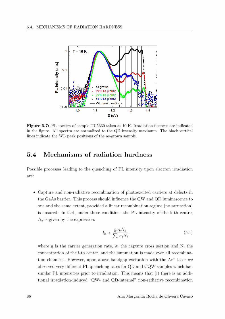
5.4. MECHANISMS OF RADIATION HARDNESS
Figure 5.7: PL spectra of sample TU5330 taken at 10 K. Irradiation fluences are indicatedin the figure. All spectra are normalized to the QD intensity maximum. The black verticallines indicate the WL peak positions of the as-grown sample.
5.4 Mechanisms of radiation hardness
Possible processes leading to the quenching of PL intensity upon electron irradiation
are:
� Capture and non-radiative recombination of photoexcited carriers at defects in
the GaAs barrier. This process should influence the QW and QD luminescence to
one and the same extent, provided a linear recombination regime (no saturation)
is ensured. In fact, under these conditions the PL intensity of the k-th centre,
Ik, is given by the expression:
Ik ∝gσkNk∑
i σiNi
(5.1)
where g is the carrier generation rate, σi the capture cross section and Ni the
concentration of the i-th center, and the summation is made over all recombina-
tion channels. However, upon above-bandgap excitation with the Ar+ laser we
observed very different PL quenching rates for QD and CQW samples which had
similar PL intensities prior to irradiation. This means that (i) there is an addi-
tional irradiation-induced “QW- and QD-internal” non-radiative recombination
86 Ana Margarida Rocha de Oliveira Cavaco

CHAPTER 5. RADIATION HARDNESS
channel that has a much greater cross section in the QW than in the QDs and
(ii) that QDs can efficiently capture carriers directly from the barrier.
� If the QDs are fed by carriers also through the WL, the defect-induced non-
radiative recombination in the WL should influence the quenching rate of the QD
PL. Therefore, an experiment with QD PL excitation below the WL band edge is
essential. The QD PL quenching observed upon sub-bandgap excitation confirms
very well the existence of an internal defect-related recombination mechanism in
the QDs and QW and its greater influence in the latter.
� The internal irradiation-induced non-radiative recombination mentioned above
may occur at defects created inside the QW (WL) and QDs as well as at the
interfaces QW(WL)/GaAs barrier, QD/QW and QD/GaAs barrier. The delo-
calization of carriers in the QW (WL) plane perpendicular to the growth direction
makes them interact with a much greater number of defects than in QDs [Schoen-
feld et al., 1998]. Thus, a priori a higher radiation hardness of the QD PL is
expected. The role of inhomogeneous strain in defect trapping at interfaces with
possible subsequent separation or annihilation has been recently discussed [Bai
et al., 2010]. It can not be excluded that the differing strain gradients influence
the defect reactions in the QW and QD to a different extent.
� Another mechanism of the “internal” defect-induced PL quenching proposed in
[Sercel, 1995] is the carrier tunnelling out of the QW or QDs to defects created in
the GaAs barrier. In fact, QDs and QWs have a different sensitivity to defects in
the adjacent barrier regions. This is due to a different degree of the wavefunction
penetration into the barrier. So, e.g. In0.13Ga0.87As QWs start to “feel” a free
surface located at distances less than about 20 nm [Chang et al., 1993]. The PL
intensity of InAs/GaAs QDs, however, only degrades for a cap thickness of 9 nm
or smaller [Fafard, 2000].
5.5 Conclusions
The current chapter is dedicated to the influence of particle irradiation on optical
emissions from quantum dots and quantum wells. A comparison is made regarding the
radiation hardness of such quantum heterostructures.
Photoluminescence experiments were performed and the results are presented and dis-
Radiation-Induced Defects in Quantum-Size Structures of A3B5 Semiconductors 87

BIBLIOGRAPHY
cussed within this chapter. A higher radiation hardness is clearly observed for quantum
dots.
The influence of the 2 MeV electron and 2.4 MeV proton irradiation on the PL of
InAs/GaAs QW and QD structures was compared. An enhanced radiation hardness
of the QDs as compared to QWs was established. The dissimilarity was related to
the different influence of defects created inside the QWs and QDs and in the adjacent
GaAs barrier on these two quantum-size structures.
Bibliography
Bai, X.-M., Voter, A., Hoagland, R., M., N., and Uberuaga, B. (2010). Science,
327:1631.
Bichsel, H. (1972). American Institute of Physics Handbook. McGraw Hill, New York,
3rd ed. edition. The electron energy loss was estimated using stopping power data.
Chang, Y.-L., Tan, I.-H., Zhang, Y.-H., Bimberg, D., Merz, J., and Hu, E. (1993).
Journal of Applied Physics, 74:5144.
Fafard, S. (2000). Applied Physics Letters, 76:2707.
Heitz, R., Veith, M., Ledentsov, N., Hoffmann, A., Bimberg, D., Ustinov, M., Kop’ev,
P., and Alferov, Z. (1997). Physical Review B, 56:10435.
Korshunov, F., Prokhorenko, T., Sobolev, N., and Kudriavstseva, E. (1992). In Mat
Res Soc Symp Proc, volume 262, page 603.
Le Ru, E., Siverns, P., and Murray, R. (2000). Applied Physics Letters, 77:2446.
Leon, R., Swift, G., Magness, B., Taylor, W., Tang, Y., Wang, K., Dowd, P., and
Zhang, Y. (2000). Applied Physics Letters, 76(15):2074 – 2076.
Mares, J., Harben, J., Thompson, A., Schoenfeld, D., and Schoenfeld, W. (2008). IEEE
Transactions on Nuclear Science, 55:763.
Piva, P., Goldberg, R., Mitchell, I., Labrie, D., Leon, R., Charbonneau, S., Wasilewski,
Z., and Fafard, S. (2000). Applied Physics Letters, 77(5):624.
Ribbat, C., Sellin, R., Grundmann, M., Bimberg, D., Sobolev, N., and Carmo, M.
(2001). Electronic Letters, 37:3.
88 Ana Margarida Rocha de Oliveira Cavaco

CHAPTER 5. RADIATION HARDNESS
Schoenfeld, W., Chen, C.-H., Petroff, P., and Hu, E. (1998). Applied Physics Letters,
73(20):2935 – 2937.
Sercel, P. (1995). Physical Review B, 51(20):14532.
Weisbuch, C. and Nagle, J. (1990). Science and Engineering of 1D and 0D Semicon-
ductor Systems. NATO ASI Series B124. Beaumont SP, Plenum, New York.
Wellmann, P., Schoenfeld, W., Garcia, J., and Petroff, P. (1998). Journal of Electronic
Materials, 27(9):1030.
Radiation-Induced Defects in Quantum-Size Structures of A3B5 Semiconductors 89

BIBLIOGRAPHY
90 Ana Margarida Rocha de Oliveira Cavaco

Chapter 6
Carrier recombination and intradot
relaxation
6.1 Introduction
Possible tunnelling of captured charge carriers off the high-lying QD energy levels to
neighbouring defects in the barrier material has been used to explain the absence of the
phonon bottleneck in the carrier intradot relaxation [Sercel, 1995]. The most obvious
way to check the existence of this mechanism is to vary the defect concentration in a
sample and to investigate the resulting changes in the time-resolved photoluminescence
(TRPL).
Irradiation creates defects with deep levels that act as non-radiative recombination
centres. The existence of stable point defects created by atomic displacements at RT
inside the In(Ga)As QDs or ultra-thin QWs has never been proven. Since the primary
defects (vacancies and interstitial atoms) are mobile at RT in GaAs (see, e.g. [Pons
and Bourgoin, 1985; Stievenard et al., 1986, 1990]) and, certainly, in InAs, it is very
likely that they are captured at the interfaces (cf. [Sobolev et al., 1996]). Moreover,
the defects increase the free energy of the crystal, so that it is only natural that the
QDs expel mobile defect components into the matrix. On the other hand, it has been
shown that some leakage of the wave function into the barrier leads to a carrier escape
to adjacent defects, thus deteriorating the QW and QD luminescence intensity [Chang
et al., 1993; Fafard, 2000].
A PL spectrum measured upon above-bandgap excitation involves QDs with different
91

6.2. CARRIER DYNAMICS
ground-state (GS) transition energies, whereas in PLE a subset of the QD ensemble
defined by the GS transition energy is probed. PLE is a powerful tool for the character-
ization of an inhomogeneous QD ensemble giving access to the shape non-uniformity of
the islands, carrier relaxation processes and non-radiative recombination [Heitz et al.,
1997].
6.2 Carrier dynamics
When talking about carrier dynamics, one must immediately consider the three major
phenomena: carrier capture, energy relaxation, and radiative recombination [Bimberg,
1999]. In particular, the capture and energy relaxation are intrinsically connected.
TRPL allows the study of carrier dynamics since all three mechanisms appear in the
same TRPL experiment: the rise kinetics accounts for the carrier capture and energy
relaxation, and the decay kinetics describes the carrier recombination [Bimberg, 1999].
Figure 6.1: Schematic diagram illustrating carrier capture from GaAs barrier into a QDvia the wetting layer and carrier relaxation within the QD [Clarke and Murray, 2008].
In order to observe luminescence at the energy of the GS or any other QD level, energy
relaxation into that level is necessary (figure 6.1). For most device applications, carriers
are either electrically injected or optically excited into the GaAs matrix surrounding the
QDs (1). Carriers are then captured, via the wetting layer (WL) (2) or immediately
into the QDs (3), and then rapidly relax to the ground state (4). Carrier capture
and relaxation occurs on the order of ps. Once carriers reach the ground state E0,
radiative recombination may take place (5) [Clarke and Murray, 2008]. Possible energy
92 Ana Margarida Rocha de Oliveira Cavaco

CHAPTER 6. CARRIER RECOMBINATION AND INTRADOT RELAXATION
relaxation mechanisms are the following ones: scattering by acoustic and/or optical
phonons, Coulomb scattering and Auger processes, interaction with nearby deep levels
and (infrared) optical inter-level transitions [Bimberg, 1999]. It has been shown that
the intradot relaxation through acoustical phonons is totally inefficient since the energy
mismatch between electron states is far too large [Benisty et al., 1991; Bockelmann and
Bastard, 1990]. Auger recombination [Efros et al., 1995] and Coulomb scattering of
free carriers [Bockelmann and Egeler, 1992; Pan, 1994] require a high density of hole
states or large free-carrier concentrations in order to obtain sufficient high relaxation
rates. At low excitation densities, both conditions are not given for small self-organized
QDs [Grundmann et al., 1995], making phonons the most likely candidates to dissipate
the energy in carrier relaxation. A strong coupling regime between electrons and LO-
phonons was observed [Heitz et al., 1997] with the formation of everlasting polarons in
InAs/GaAs QDs [Hameau et al., 1999].
The structural properties, in particular the shape and composition profile, of self-
organized In(Ga)As/GaAs QDs strongly affect the exciton dynamics [Heitz et al., 2002].
The low symmetry and inhomogeneous strain provide in general for distinctively dif-
ferent electron and hole wave functions [Stier et al., 1999] and enable one to engineer
the electron-hole overlap, i.e. the oscillator strength, as well as the local charge den-
sity, i.e. the polar exciton-LO-phonon coupling strength. The coupling strength, being
proportional to the local charge density [Schmitt-Rink et al., 1987], depends on the
difference of the electron and hole wave functions [Stier et al., 1999] and, thus on the
particular structural properties of the QDs: the effect is pronounced for a pyramidal
but strongly quenched for a flat shape. Thus, the ground state lifetime is expected to
be shorter (large overlap integral) in the flat InGaAs QDs, whereas the stronger polar
exciton-LO-phonon interaction (large local charge density) should provide for faster
relaxation in the pyramidal InAs QDs. Depending on the QD shape, relaxation- or
recombination-limited exciton dynamics should be observed.
6.3 Equipment and measurement conditions
The cw PL and PLE experiments were performed in a continuous-flow He cryostat at
temperatures between 7 and 300 K. A tungsten lamp dispersed by a 0.27 m double-
grating monochromator served as a low density, tunable light source. The emission was
spectrally dispersed by a 0.3 m double-grating monochromator and detected with a
cooled Ge diode using lock-in techniques. The measurement techniques and equipment
Radiation-Induced Defects in Quantum-Size Structures of A3B5 Semiconductors 93

6.4. PROTON-IRRADIATED SAMPLES
have been thoroughly discussed in sections 3.2.1 and 3.2.2.
The TRPL measurements were carried out at 2 K using a single photon counting
technique. The exciting Ti+-sapphire laser system including an OPO, with spectrally
narrow (<1 meV) pulses, operated at 790 nm (1.569 eV) for above-bandgap excitation
or at 858 nm (1.445 eV) for resonant excitation with a pulse width of 2 ps. The emitted
light was dispersed by a subtractive double-grating monochromator and detected with
a multi-channel plate photomultiplier with an S1-cathode in the photon-counting mode.
The time resolution of the detecting system was about 20 ps. The averaged excitation
density within the pulse was 250 W/cm2. The experimental facilities and techniques
are described in details in section 3.2.3.
6.4 Proton-irradiated samples
6.4.1 Samples
The samples used in the proton-irradiation studies (TU5411 and TU5330) were grown
by metal-organic chemical vapour deposition and have the following structure: a GaAs
buffer layer was grown on top of a GaAs substrate, the active layer together with GaAs
cladding layers were placed between two AlGaAs barriers, with a GaAs capping layer
on top of the whole structure. Sample TU5411 has an active layer composed by a QD
layer, with a dot density of (3–5)×1010 cm2, overgrown by a 2 nm In0.25Ga0.75As QW.
Sample TU5330 has a dot density of ≈ 109 cm2 in an active layer composed by a single
QD layer. The irradiation by 2.4 MeV protons with fluences in the range from 1×10¹²
to 1×1014 cm−2 was performed at room temperature using a Van de Graaff accelerator.
A more detailed characterization of these samples can be found in sections 4.2 and 4.3.
6.4.2 Results
Figure 4.15 shows the FTIR PL spectrum of the as-grown sample TU5411 taken at
10 K upon excitation with the 488 nm line of an Ar+ laser. The energies assigned in
the graph represent the detection and excitation energies used in TRPL measurements
(see figure 6.2) on the same sample. For sample TU5411, kinetic curves were fitted
using exponential functions including a rise and a decay time. Table 6.1 shows the
rise and decay times obtained from the fitting as a function of irradiation fluence. For
94 Ana Margarida Rocha de Oliveira Cavaco

CHAPTER 6. CARRIER RECOMBINATION AND INTRADOT RELAXATION
Table 6.1: TRPL rise and decay times of proton-irradiated samples TU5411.
fluence Eexc = 1.57 eV Eexc = 1.14 eV Eexc = 1.12 eVp/cm2 τr, ps τd, ps τr, ps τd, ps τr, ps τd, ps
as-grown 397 896 648 700 660 6621×1013 353 848 666 667 489 8322×1013 340 880 443 873 467 8935×1013 196 958 273 939 250 9691×1014 104 928 150 944 131 955
all samples the detection was performed at the ground state energy, E = 1.04 eV (see
figure 4.15), and the excitation was performed at the following energies (see figures 4.15
and 6.3b): E = 1.12 eV (a sublevel of the first excited state), E = 1.14 eV (another
sublevel of the first excited state) and E = 1.57 eV (above-GaAs bandgap excitation).
According to the results shown in figure 6.2 and table 6.1, the increasing defect con-
centration with increasing dose does not affect the lifetime of the ground state exciton,
always showing a single-exponential decay. This is true both for above-GaAs bandgap
and resonant excitation into the first excited state of QDs. A more or less constant de-
cay time around 900 ps is observed. The data suggest tunnelling from the QD ground
state to defect states to be negligible at the proton irradiation dose used here. The
rise time is clearly affected by irradiation showing a decrease from around 400 ps to
100 ps as irradiation fluence increases. The long rise time in the reference sample is
attributed to slowed down intradot relaxation [Heitz et al., 2001]. Carrier migration
in the GaAs barrier is negligible for the rise time due to the AlGaAs diffusion barriers
reducing the average diffusion length to below ∼50 nm. If one looks at the change of
the rise time as a function of the excitation energy, an increase can be seen going from
above-bandgap excitation to the resonant excitation into excited states. This increase
is more pronounced for the as-grown sample and vanishes for the heavier irradiated
one. The reduced PL rise time and the decreased PL efficiency in the irradiated sam-
ples suggest tunnelling from excited QD states to defects. The increasing tunnelling
probability with increasing defect concentration quenches the excitation efficiency and
the rise time (see figures 6.2 and 6.3).
Figure 6.3a shows PL spectra of sample TU5411 for various proton irradiation fluences
(as indicated in the figure) taken at 7 K. The PL intensity behaviour is the same
as that observed for the electron-irradiated samples in chapter 5, viz., the intensity
Radiation-Induced Defects in Quantum-Size Structures of A3B5 Semiconductors 95

6.4. PROTON-IRRADIATED SAMPLES
Figure 6.2: Rise (open circles) and decay (solid circles) times obtained from TRPL mea-surements of sample TU5411. The detection energy was at the ground state transition. Theexcitation energies are indicated in the graphs.
96 Ana Margarida Rocha de Oliveira Cavaco

CHAPTER 6. CARRIER RECOMBINATION AND INTRADOT RELAXATION
Figure 6.3: (a) PL and (b) PLE spectra of sample TU5411 for various proton irradiationfluences, measured at 7 K. The PLE spectra were recorded at the QD PL intensity maximum.
Radiation-Induced Defects in Quantum-Size Structures of A3B5 Semiconductors 97

6.4. PROTON-IRRADIATED SAMPLES
decreases as the irradiation fluence increases. Figure 6.3b represents PLE spectra
of the same sample for various proton irradiation fluences. LO-phonon resonances,
excited states and WL energy positions are indicated. The detection occurred at the
QD PL maximum, Edet = 1.04 eV, the ground state energy position. An increase upon
irradiation of the PLE intensity at energies corresponding to the low-lying QD excited
states can be observed (figure 6.3b).
Figure 6.4a shows PLE spectra plotted vs. the excess excitation energy
∆E = Eexc − Edet of the as-grown sample TU5330 taken at different temperatures
(as indicated in the graph). The detection was performed at the QD PL maximum.
The spectra are normalized to the detection energy and to the second excited state
intensity. Figure 6.4b presents PLE spectra of sample TU5330 for various proton flu-
ences, recorded at the QD PL maximum at 7 K. The spectra are normalized to the
intensity above the GaAs bandgap.
As referenced before, an increase of the PLE intensity at energies corresponding to the
low-lying QD excited states is observed upon irradiation. The effect is particularly well
seen in figure 6.4b, where the PLE intensities for all fluences have been normalized to
that of the as-grown sample at energies exceeding the GaAs bandgap, and in the contour
plots (figure 6.5). Qualitatively similar effects are observed when the temperature is
increased (figure 6.4a) or a reverse bias is applied to a diode structure with the dots
located in the space charged region [Guffarth et al., 2003, 2002]. The radiation defects
shift the Fermi level towards the middle of the bandgap, thus emptying the low-lying
QD states from spectator carriers allowing the resonant absorption to occur. The
results (see figure 6.4a) unambiguously demonstrate a slow relaxation between the first
excited and the ground state, which accelerates with increasing temperature supporting
the notion of inelastic phonon scattering. In the case of a temperature increase, the
important effect is the growth of the phonon density which accelerates the relaxation
and helps overcome the phonon bottleneck [Heitz et al., 2001].
Figure 6.5 shows contour plots of the QD PL intensity as a function of the detection
energy and the excess excitation energy ∆E = Eexc − Edet taken at 7 K for the as-
grown and proton-irradiated samples TU5330 (the irradiation fluences are indicated
in the graphs). The white lines denote PLE resonances from the excited states and
LO-phonons. For the as-grown and the two lowest irradiation fluences samples, the
first excited state resonance is not observed, appearing only for the highest irradiation
fluence shown (see also figure 6.4).
98 Ana Margarida Rocha de Oliveira Cavaco

CHAPTER 6. CARRIER RECOMBINATION AND INTRADOT RELAXATION
Figure 6.4: PLE spectra of sample TU5330. a) PLE spectra vs. the excess excitation energy∆E = Eexc−Edet of the as-grown sample TU5330 taken at different temperatures. Detectionwas performed at the QD PL maximum. The spectra are normalized to the detection energyand to the second excited state intensity. b) PLE spectra of sample TU5330 for variousproton fluences, recorded at the QD PL maximum at 7 K. The spectra are normalized to theintensity above the GaAs bandgap.
Radiation-Induced Defects in Quantum-Size Structures of A3B5 Semiconductors 99

6.4. PROTON-IRRADIATED SAMPLES
Figure 6.5: Contour plots of the QD PL intensity measured at 7 K as a function of thedetection energy and the excess excitation energy ∆E = Eexc - Edet for the as-grown andproton-irradiated samples TU5330. The white lines denote PLE resonances from the excitedstates and LO-phonons. The irradiation fluences are indicated in the graphs.
Usually the defects reduce the lifetime of non-equilibrium carriers and, consequently,
their diffusion length, thus limiting the carrier supply to the radiative recombination
centres and quenching the PL intensity. However, because of the presence of the closely
spaced AlGaAs barriers, the carrier capture by the QDs in the samples under study
is not diffusion-limited. That is why no difference in the quenching factor of the PL
intensity is observed at a given irradiation fluence for the above-bandgap and below-
bandgap excitation for all energies above the n = 2 QD excited state (figure 6.3).
Thus, the loss of carriers occurs mainly in the dots themselves. A probable reason of
this effect is a tunnelling out of the dots to adjacent radiation-induced non-radiative
recombination centres, as described in section 5.4.
100 Ana Margarida Rocha de Oliveira Cavaco

CHAPTER 6. CARRIER RECOMBINATION AND INTRADOT RELAXATION
6.4.3 Discussion
No influence of the irradiation on the PL decay kinetics from the ground state is
observed (figure 6.2) since the decay times are essentially the same for the as-grown
and irradiated samples, as well as for the above- and below-bandgap excitation. This
situation is only possible if no defects are created inside the QDs, showing no alternative
path for the carriers to recombine but trough radiative recombination. These results
agree with those shown in section 6.5 where a second decay component appearing after
irradiation was ascribed to defects created close to or inside the QDs.
However, the rise time shortens by a factor of four for the maximum fluence used
(1×10¹⁴ p/cm2), both for the excitation into the barrier (figure 6.2a) and into the
sublevels of the first excited state at 1.140 eV and 1.123 eV (figure 6.2b and c). This
means that the rise time shortening upon above-bandgap excitation is caused by a
carrier (exciton) loss in the QDs and not by any reduction of the diffusion length in
the barrier or the WL. The effect can be explained by the tunnel escape of the carriers
to adjacent defects. The ground state, having a more localized wave function than the
excited ones, remains essentially “undamaged”.
The rise time increases as the excitation energy decreases (see table 6.1), mainly for
the as-grown sample. For the heavier irradiated sample this behaviour vanishes. The
resonant excitation does not account for any kind of diffusion or transport, so this
increase is related only to relaxation mechanisms, showing a more efficient path from
the barrier than from the excited states to the ground state. If the relaxation process
would depend on a cascade of events through the different intermediate states, a higher
rise time for the barrier excitation would be expected. Since this is not the case, the
existence of a bottleneck at the first excited state becomes a possible explanation.
Moreover, the results for the irradiated samples show that an alternative path owing
to the irradiation exists to overcome this bottleneck.
6.5 Electron-irradiated samples
6.5.1 Samples
Two types of samples were grown using MOCVD under identical conditions and sub-
jected simultaneously to electron irradiation. The samples differed only with respect
to the active region. In the sample 1×QD (TU3904), the active region consisted of
Radiation-Induced Defects in Quantum-Size Structures of A3B5 Semiconductors 101

6.5. ELECTRON-IRRADIATED SAMPLES
one layer layer of self-assembled InGaAs/GaAs QDs with density 5×1010 cm−2 on a
thin wetting layer (WL). Sample CQW (TU3903) contained two coupled InAs/GaAs
quantum wells separated by 1 nm. The active layer together with the GaAs cladding
layers was placed between two Al0.3Ga0.7As barriers (see figure 4.1). The samples are
thoroughly characterized in section 4.1. The irradiation by 2 MeV electrons with flu-
ences in the range of 2×10¹⁵ to 2×1017 cm−2 was performed at room temperature using
a Van de Graaff accelerator.
6.5.2 Results
The results of the TRPL measurements on 1×QD and CQW samples, upon above-
bandgap excitation (Eexc = 1.569 eV), are shown in figure 6.6. The rise (τr) and decay
(τd) times, obtained from the exponential fitting, are given in table 6.2. The transients
prior to irradiation can be fitted with single values of τr and τd.
Figure 6.6: PL transients taken at 2 K of the as-grown and electron-irradiated CQW and1×QD samples. Above-bandgap excitation occurred at an energy of 1.569 eV. Detectionenergy was 1.230 eV for 1×QD and 1.340 eV for CQW, respectively.
102 Ana Margarida Rocha de Oliveira Cavaco
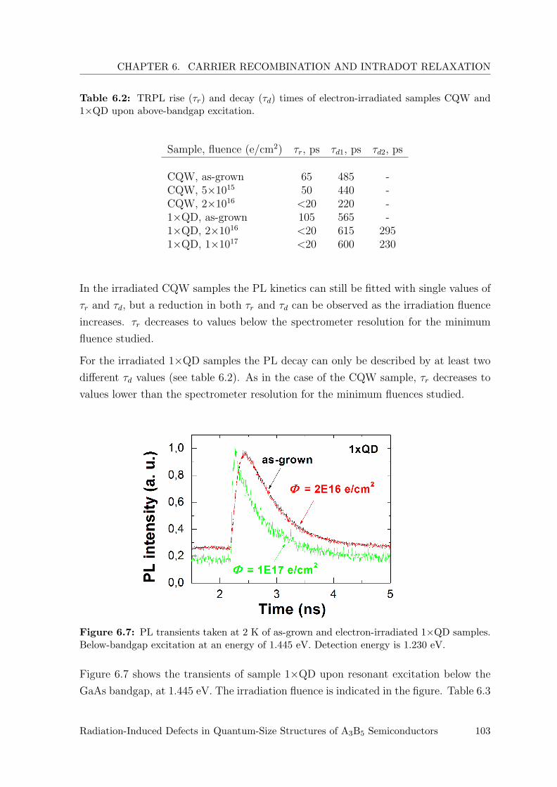
CHAPTER 6. CARRIER RECOMBINATION AND INTRADOT RELAXATION
Table 6.2: TRPL rise (τr) and decay (τd) times of electron-irradiated samples CQW and1×QD upon above-bandgap excitation.
Sample, fluence (e/cm2) τr, ps τd1, ps τd2, ps
CQW, as-grown 65 485 -CQW, 5×10¹⁵ 50 440 -CQW, 2×10¹⁶ <20 220 -1×QD, as-grown 105 565 -1×QD, 2×10¹⁶ <20 615 2951×QD, 1×10¹⁷ <20 600 230
In the irradiated CQW samples the PL kinetics can still be fitted with single values of
τr and τd, but a reduction in both τr and τd can be observed as the irradiation fluence
increases. τr decreases to values below the spectrometer resolution for the minimum
fluence studied.
For the irradiated 1×QD samples the PL decay can only be described by at least two
different τd values (see table 6.2). As in the case of the CQW sample, τr decreases to
values lower than the spectrometer resolution for the minimum fluences studied.
Figure 6.7: PL transients taken at 2 K of as-grown and electron-irradiated 1×QD samples.Below-bandgap excitation at an energy of 1.445 eV. Detection energy is 1.230 eV.
Figure 6.7 shows the transients of sample 1×QD upon resonant excitation below the
GaAs bandgap, at 1.445 eV. The irradiation fluence is indicated in the figure. Table 6.3
Radiation-Induced Defects in Quantum-Size Structures of A3B5 Semiconductors 103

6.5. ELECTRON-IRRADIATED SAMPLES
Table 6.3: TRPL rise and decay times of electron-irradiated samples 1×QD upon resonantexcitation.
Sample, fluence (e/cm2) τr, ps τd1, ps τd2, ps
1×QD, as-grown 117 522 -1×QD, 2×10¹⁶ 113 489 -1×QD, 1×10¹⁷ <20 619 126
summarizes the time constants obtained from the exponential fitting to the data. As
for the above-bandgap excitation, the curve for the as-grown sample was fitted using
single rise and decay times and that for the heaviest irradiated sample with one rise
time and two decay times. Comparing figure 6.6 with figure 6.7 and table 6.2 with table
6.3, a striking difference can be noted. Sample 1×QD with Φ = 2×1016 cm−2 presents
a completely distinct behaviour when excited above and below the GaAs bandgap.
While upon above-bandgap excitation, this sample exhibited a behaviour similar to
that of the heavily irradiated sample, for below-bandgap excitation it behaves like the
as-grown sample. This behaviour can be explained regarding the relation between the
wave function penetration depth into the barrier and the distance between the dots
and defects.
Figure 6.8: PLE spectra of sample 1×QD for various electron irradiation fluences, measuredat 7 K. The PLE spectra were recorded at the QD PL maximum. The spectra are normalizedto the intensity above the GaAs bandgap.
104 Ana Margarida Rocha de Oliveira Cavaco

CHAPTER 6. CARRIER RECOMBINATION AND INTRADOT RELAXATION
Figure 6.8 shows PLE spectra of sample 1×QD measured at 7 K for various electron
irradiation fluences. The PLE spectra were recorded at the QD PL maximum and are
normalized to the intensity at energies above the GaAs bandgap. A striking feature
of the PLE spectra is the increase upon irradiation of the PLE intensity at energies
corresponding to the low-lying QD excited states. The same behaviour was observed for
the proton-irradiated sample (figure 6.4). These results indicate a higher probability of
the non-radiative recombination of the photoexcited carriers in the barrier than inside
the dots. The resonances observed in the PLE spectra (see figure 6.8) are attributed to
excited state transitions, although the high QD density of these samples never allowed
the observation of bands belonging to excited states in the nonresonantly excited PL
spectra (see section 4.1). No resonance corresponding to the WL position could be
observed for these samples, either.
6.5.3 Discussion
There is a clear impact of the introduced radiation defects on the rise and decay times
in both CQW and QD samples (figures 6.6 and 6.7). The fast rise time is an indication
of an effective carrier relaxation to the QD ground state. The decay time is reduced due
the increase of non-radiative recombination caused by the radiation-induced defects.
The reduced PL rise time and the decreased PL efficiency in the irradiated samples
suggest a tunnelling of the carriers/excitons from the dots to adjacent defects.
The electron irradiation with high fluences induces a second process with a shorter PL
decay time. The higher τd characterizes the as-grown sample. Since not all QDs in a
sample are disturbed by defects, the slow decay component is still observed even after
irradiation. The shorter PL decay time that does not change with irradiation fluence is
ascribed to the existence of QDs perturbed by defects inside or immediately adjacent
to them.
The heaviest electron irradiation used in this work induces such a high concentration of
defects that there is no way for the QDs to escape an interaction with the latter since the
distance between QDs and radiation-induced defects decreases with increasing fluence.
For the medium irradiation dose, the radiation hardness depends on the excitation
wavelength due to the wave function penetration depth of the energy levels involved.
Qualitatively the same behaviour has been observed upon resonant (below bandgap)
excitation for the CQW sample. However, a poor signal-to-noise ratio and a strong
substrate PL impeded a reliable quantitative evaluation.
Radiation-Induced Defects in Quantum-Size Structures of A3B5 Semiconductors 105

6.6. CONCLUSIONS
6.6 Conclusions
The influence of high-energy electron and proton irradiation on the time-resolved photo-
luminescence and the photoluminescence excitation spectra of quantum dot and quan-
tum well InGaAs/GaAs structures is reported and discussed. A clear interaction of the
created defects and the quantum dot structures is observed for both types of particle
irradiation. The results suggest expulsion of the defects by the dots, resulting in a high
radiation hardness of the latter.
For proton-irradiated samples, only the rise kinetics is affected by irradiation. The
decay kinetics remains unchanged probably due to the fact that QDs have the ability,
due to strain fields, of expelling mobile defects. The PL rise time gets shorter with
increasing irradiation fluence owing to carrier escape out of the excited QD states to
adjacent radiation-induced defects.
For the electron-irradiated samples, the decay kinetics of the as-grown QWs and QDs
can be described by a single time constant. The irradiated QWs still exhibit the single
exponential decay, however, with a shorter time constant, whereas the second, faster
component appears in the PL decay of QDs along with the component present prior
to irradiation. Thus, an interaction of confined carriers with radiation-induced defects
located inside or very close to the QDs was observed. An influence of the energy
level wave function penetration depth was found on the carrier dynamics in irradiated
samples.
For the sample configuration used (two AlGaAs diffusion barriers surrounding the QD
plane), the main part of the carrier loss due to introduced radiation damage occurs in
the dots, even for the excitation of the GaAs barrier.
The decreasing PL intensity upon irradiation reflects the decreasing excitation effi-
ciency originating from 1) tunnelling out of excited QD states due to slow relaxation
at low temperatures and 2) efficient non-radiative recombination in the barrier, when
carriers escape thermally from the QDs at elevated temperatures.
The difference in the radiation fluences between the electron and proton irradiations is
of three orders of magnitude for the heaviest irradiated samples. According to figure 2.7
the difference in average energy transmitted to an atom at MeV energies is less than an
order of magnitude for electrons when compared to protons. So, the heavily electron-
irradiated samples probably have, at least, two orders of magnitude more defects than
the proton-irradiated ones. This is why a second decay time is not observed for the
106 Ana Margarida Rocha de Oliveira Cavaco

CHAPTER 6. CARRIER RECOMBINATION AND INTRADOT RELAXATION
proton-irradiated samples.
Bibliography
Benisty, H., Sotomayor-Torres, C., and Weisbuch, C. (1991). Physical Review B,
44(19):10945.
Bimberg, D. (1999). Semiconductors, 33(9):951.
Bockelmann, U. and Bastard, G. (1990). Physical Review B, 42:8947.
Bockelmann, U. and Egeler, T. (1992). Physical Review B, 46:15574.
Chang, Y.-L., Tan, I.-H., Zhang, Y.-H., Bimberg, D., Merz, J., and Hu, E. (1993).
Journal of Applied Physics, 74:5144.
Clarke, E. and Murray, R. (2008). Handbook of Self Assembled Semiconductor Nanos-
tructures for Novel Devices in Photonics and Electronics, chapter 3 – Optical Proper-
ties of In(Ga)As/GaAs Quantum Dots for Optoelectronic Devices, page 84. Elsevier,
The Netherlands.
Efros, A., Kharchenko, V., and Rosen, M. (1995). Solid State Communications, 93:281.
Fafard, S. (2000). Applied Physics Letters, 76:2707.
Grundmann, M., Stier, O., and Bimberg, D. (1995). Physical Review B, 52:11969.
Guffarth, F., Heitz, R., Geller, M., Kapteyn, C., Born, H., Hoffmann, A., Bimberg, D.,
Sobolev, N., and Carmo, M. (2003). Applied Physics Letters, 82:1941.
Guffarth, F., Heitz, R., Kapteyn, C., Heinrichsdorff, F., and Bimberg, D. (2002).
Physica E, 13:278.
Hameau, S., Guldner, Y., Verzelen, O., Ferreira, R., Bastard, G., Zeman, J., Lemaıtre,
A., and Gerard, J. (1999). Physical Review Letters, 83:4152.
Heitz, R., Born, H., Guffarth, F., Stier, O., Schliwa, A., Hoffmann, A., and Bimberg,
D. (2001). Physical Review B, 64:241305(R).
Heitz, R., Born, H., Guffarth, F., Stier, O., Schliwa, A., Hoffmann, A., and Bimberg,
D. (2002). Physica Status Solidi A, 190:499–504.
Radiation-Induced Defects in Quantum-Size Structures of A3B5 Semiconductors 107

BIBLIOGRAPHY
Heitz, R., Veith, M., Ledentsov, N., Hoffmann, A., Bimberg, D., Ustinov, M., Kop’ev,
P., and Alferov, Z. (1997). Physical Review B, 56:10435.
Pan, J. (1994). Physical Review B, 49:2536.
Pons, D. and Bourgoin, J. (1985). Journal of Physics C: Solid State Physics, 18:3839.
Schmitt-Rink, S., Miller, D., and Chemla, D. (1987). Physical Review B, 35:8113.
Sercel, P. (1995). Physical Review B, 51(20):14532.
Sobolev, N., Korshunov, F., Sauer, R., Thonke, K., Konig, U., and Presting, H. (1996).
Journal of Crystal Growth, 167:502.
Stier, O., Grundmann, M., and Bimberg, D. (1999). Physical Review B, 59(8):5688–
5701.
Stievenard, D., Boddaert, X., and Bourgoin, J. (1986). Physical Review B, 34:4048.
Stievenard, D., Boddaert, X., Bourgoin, J., and von Bardeleben, H. (1990). Physical
Review B, 41:5271.
108 Ana Margarida Rocha de Oliveira Cavaco
Chapter 7
Influence of defects on the
temperature dependence of the PL
intensity
7.1 Introduction
In most QD applications, the devices are expected to work at room temperature or
even higher. However, the luminescence is often quenched at temperatures signifi-
cantly below 300 K, cf. chapter 4. Understanding the temperature dependence of the
QD emission and the factors influencing it is important to building efficient and tem-
perature insensitive lasers. There is a consensus in the literature that the quenching
phenomenon observed in PL spectra is linked to thermal escape of carriers from the
QDs to the surrounding matrix, followed by non-radiative recombination [Bacher et al.,
1991; Brusaferri et al., 1996; Le Ru et al., 2003; Polimeni et al., 1999; Wasilewski et al.,
1999]. Point defects and defect clusters in the matrix are suspected to be responsible
for the trapping of escaped carriers. In fact, they serve as local non-radiative recom-
bination centres for electron-hole pairs, and thus reduce the luminescence efficiency
of optical devices. Understanding the real role of defects in the performance of QD
devices and the optimization of the defect concentration for achieving the best QD
emission stability is a challenging task. It has been shown in ref. [Baidus et al., 2005]
that elimination of defects via growth treatment using tetrachloromethane eliminates
the quenching of PL at room temperature.
In this chapter, we have extended the investigations to the case of samples containing a
109

7.2. EQUIPMENT AND MEASUREMENT CONDITIONS
well-defined amount of intentionally introduced defects. These defects were introduced
in a controlled way by proton or electron irradiation.
7.2 Equipment and measurement conditions
Photoluminescence (PL) was measured at sample temperatures ranging from 10 to
300 K in a closed-cycle or continuous-flow cryostat. The PL was excited either with
an Ar+ laser (488 nm) or a He-Ne laser (632.8 nm). The spectra were recorded with
a Fourier-transform infrared (FTIR) spectrometer with a cooled Ge detector or with
a Spex grating monochromator and an InGaAs photodiode using standard lock-in
technique. The experimental facilities and techniques are described in detail in section
3.2.1.
7.3 Experimental results
7.3.1 Laser structures
Figure 7.1: Temperature dependence, from 10 to 300 K, of the PL of samples 1×QD(TU3904), as-grown and irradiated. The irradiation fluence is indicated in the graph. Left:QD PL energy peak position; right: full width at half maximum (FWHM) of the QD PLband.
Three types of samples were grown using MOCVD under identical conditions according
to the layer sequence shown in figure 4.1. The samples differ only with respect to the
active region: sample 1×QD (TU3904) is composed of one layer of self-assembled
InAs/GaAs QDs on a thin WL; sample CQW (TU3903) is formed by two coupled
InAs QWs separated by 1 nm GaAs; sample 5×QD (TU3972) contains five QD layers
110 Ana Margarida Rocha de Oliveira Cavaco

CHAPTER 7. INFLUENCE OF DEFECTS ON THE TEMPERATURE DEPENDENCE
OF THE PL INTENSITY
separated by 20 nm GaAs. The active layer together with the GaAs cladding layers
are placed between two Al0.3Ga0.7As barriers. The structure was grown on top of a
GaAs substrate and a GaAs buffer layer. The samples are thoroughly characterized in
section 4.1. The irradiation by 2 MeV electrons with fluences in the range from 2×10¹⁵
to 2×1017 cm−2 was performed at room temperature using a Van de Graaff accelerator.
Figure 7.2: Arrhenius plots of the PL intensity for samples 1×QD (TU3904), as-grown andirradiated. The irradiation fluence is indicated on the graph.
Figure 7.1 shows the QD PL band energy position (on the left) and full width at
half maximum (FWHM) (on the right) as a function of temperature for the as-grown
and for an irradiated sample 1×QD (TU3904). The irradiation fluence was equal to
5×10¹⁶ e/cm2. No significant differences have been observed for the temperature de-
pendences of the PL band energy position or the FWHM with increased concentration
of radiation defects (see figure 7.1). For a more detailed description of these depen-
dences see section 4.1. Figure 7.2 shows an Arrhenius plot of the PL intensity for
the same samples. Here the difference between the as-grown and irradiated samples is
clearly visible.
7.3.2 Samples subjected to CCl4 treatment
InAs/GaAs QD heterostructures were grown by Atmospheric Pressure Metal-Organic
Vapor Phase Epitaxy (AP-MOVPE). Two kinds of samples were prepared. Samples
Radiation-Induced Defects in Quantum-Size Structures of A3B5 Semiconductors 111

7.3. EXPERIMENTAL RESULTS
NN4190 with no treatment with tetrachloromethane (CCl4) were grown in standard
conditions. Samples NN4184 were subjected, during the growth process, to a treatment
with tetrachloromethane (CCl4), which had been shown to decrease the defect concen-
tration in the GaAs matrix [Karpovich et al., 2004]. For a more detailed description of
these samples see section 4.5. The irradiation by 180 keV protons with fluences ranging
from 1011 to 1012 p/cm2 was performed at RT using a Van de Graaff accelerator.
Figure 7.3: PL spectra of two QD/QW heterostructures, left: NN4190, and right: NN4184,taken at two different temperatures. The units are indicated in the plots and are the samefor all spectra. The most important bands are identified.
Samples NN4190 and NN4184 were found to show different trends in the variation of the
PL intensity with measurement temperature. The temperature dependence of the QD
PL intensity from sample NN4190 exhibits a typical quenching at room temperature.
Figure 7.3 (left) shows two PL spectra of sample NN4190 recorded at 12 and 298 K.
At 12 K, emission bands from the QDs, QW and GaAs can be observed. The rather
low inhomogeneous broadening observed for the QD emission band is an indication of
a narrow QD size dispersion. Beyond the main peak of the QD emission, the spectrum
shows a band slightly above 1 eV that originates from excited states in the dots. In
112 Ana Margarida Rocha de Oliveira Cavaco

CHAPTER 7. INFLUENCE OF DEFECTS ON THE TEMPERATURE DEPENDENCE
OF THE PL INTENSITY
Figure 7.4: Temperature dependence of the integrated PL intensity (normalized to the low-temperature value) for an as-grown and two proton-irradiated NN4190 samples. Irradiationfluences are indicated on the plot.
contrast, the decrease in the PL intensity of the QD ground state emission peak is very
small for sample NN4184 (see figure 7.3, right), less than by a factor of 2 up to room
temperature.
Figure 7.4 shows the experimental temperature dependence of the integrated PL inten-
sity for an as-grown and two proton-irradiated NN4190 samples. The intensity values
are all normalized to the low-temperature value. The irradiation fluences are indicated
on the plot.
Figure 7.5 shows the experimental temperature dependence of the integrated PL inten-
sity for an as-grown and two proton-irradiated NN4184 samples. The intensity values
are all normalized to the low-temperature value. The irradiation fluences are indicated
on the plot. The blue asterisks show the temperature dependence of the PL emission
band of the as-grown QW sample.
Figure 7.6 shows the experimental temperature dependence of the integrated QD PL
intensity for two values of the beam power of the Ar+ laser as indicated in the plot. The
estimated power densities on the sample are 1 mW/cm2 and 1 W/cm2, respectively.
The results are for the as-grown sample NN4190.
These results being experimental were included here but are discussed in section 7.6
Radiation-Induced Defects in Quantum-Size Structures of A3B5 Semiconductors 113

7.3. EXPERIMENTAL RESULTS
Figure 7.5: Temperature dependence of the integrated PL intensity (normalized to thelow-temperature value) for an as-grown and two proton-irradiated NN4184 samples. Theirradiation fluences are indicated on the plot. The blue asterisks show the temperaturedependence of the PL emission band of the as-grown QW sample.
Figure 7.6: Experimental temperature dependence of the integrated QD PL intensity fortwo values of the beam power of the Ar+ laser as indicated in the plot (estimated powerdensity on the sample 1 mW/cm2 and 1 W/cm2, respectively). Results are for the as-grownsample NN4190.
114 Ana Margarida Rocha de Oliveira Cavaco
CHAPTER 7. INFLUENCE OF DEFECTS ON THE TEMPERATURE DEPENDENCE
OF THE PL INTENSITY
together with the calculated results presented in section 7.5.
7.4 Model
The work has been performed in collaboration with Prof. Dr. M. Vasilevskiy from the
University of Minho. The main objective of the described model is to explain the
trends of the ground-state emission from the QDs.
Assumptions:
� Just one electron energy level, Ec - EeQD;
� Just one hole energy level, Ev - EhQD;
� The dots are embedded in a QW with
– The lowest possible electron energy, Ec - EeQW ;
– The lowest possible hole energy, Ev - EhQW ;
� The GaAs matrix is considered intentionally doped with acceptors, and their
ionization energy is Ea.
� The modulation doping affects the confinement potential profiles, but it is as-
sumed that this effect is taken into account in the characteristic energies intro-
duced above.
The model band structure is presented in figure 7.7. Besides the energies referenced
above, it includes also the Fermi level (EF ), the quasi-Fermi level (F ) and the trap
energy level (Et). As usual, the bandgap energy is denoted by Eg, the conduction band
minimum by Ec and the valence band maximum by Ev.
7.4.1 Heterostructure in equilibrium
At equilibrium, the majority carriers (holes in this case) are distributed between ac-
ceptors, GaAs barriers, QDs and QW. In order to achieve an analytical solution, an
effective homogeneous system representing the heterostructure is considered. This im-
plies the use of an effective three-dimensional (3D) concentration of QDs,
Radiation-Induced Defects in Quantum-Size Structures of A3B5 Semiconductors 115

7.4. MODEL
Figure 7.7: Model band structure of the GaAs/GaInAs(QW)/InAs(QD) heterostructure.
N(3D)QD =
N(2D)QD
w(7.1)
where N(2D)QD is the usual two-dimensional dot density referred in sample description,
and w is a characteristic thickness of the system at equilibrium. w is of the order of
the overall thickness of the buffer and capping layers, or the Debye length, whichever
is smaller. Similarly to the QDs, an effective 3D density of states for the QW is
introduced,
N(3D)QW =
1
w
m∗kT
π~2, (7.2)
where m∗ is the effective mass of the carriers. Then, hole concentrations in the QDs,
QW, and GaAs matrix are given by the standard statistical relations:
pQD = N(3D)QD
[
βhQD exp
(
EF + Eg − EhQD
kT
)
+ 1
]−1
, (7.3)
pQW = N(3D)QW ln
[
exp
(
−EF − Eg + EhQW
kT
)
+ 1
]
, (7.4)
pM = NV F1/2
(
−EF + Eg
kT
)
, (7.5)
116 Ana Margarida Rocha de Oliveira Cavaco

CHAPTER 7. INFLUENCE OF DEFECTS ON THE TEMPERATURE DEPENDENCE
OF THE PL INTENSITY
where EF is the Fermi level position with respect to the bottom of the GaAs conduction
band (Ec), Eg is the bandgap energy of GaAs, βhQD is the degeneracy factor of the QD
hole level, and
NV =[(mhh +mlh) kT ]
3
2
√2π
3
2~3, (7.6)
where mhh and mlh are heavy and light hole effective masses, respectively, N(3D)QW is
given by equation 7.2 with m∗ = mhh, and F1/2 is the Fermi integral. The Fermi level
position can be found from the neutrality equation
pQD + pQW + pM = Na
[
1 +1
4exp
(
Ea − EF − Eg
kT
)]−1
, (7.7)
where Na is the acceptor concentration and, the degeneracy factor of the acceptor level
has been taken equal to 4.
7.4.2 Heterostructure under illumination
The assumption of relatively low excitation intensity shall be considered now in order
to be possible to consider the majority carriers at equilibrium and described by the
same (true) Fermi level.
It is also assumed that the photogenerated minority carriers (electrons) are distributed
between QDs, QW, and GaAs matrix, and that the equilibrium between the QD, QW,
and matrix states is established much faster than the recombination occurs, meaning
it is reached within the photocarrier’s lifetime. This last assumption is hardly realistic
at low temperatures. The experimental results (see figures 7.4 and 7.5) show that the
major differences occur for T ≥ 100 K. This is the temperature range where the model
is expected to work. In this temperature region, phonon-assisted processes of carrier
capture, relaxation, and excitation into higher energy states can be fast enough to
justify the (pseudo-) equilibrium assumption. It is also assumed, for simplicity, that
the electrons in the matrix are non-degenerate.
It is now possible to introduce a quasi-Fermi level (F ) for the electrons and express the
(3D) electron concentrations in different states using relations analogous to equations
(7.3), (7.4) and (7.5) (and in close analogy to what has been done in ref. [Baidus et al.,
2005]),
Radiation-Induced Defects in Quantum-Size Structures of A3B5 Semiconductors 117

7.4. MODEL
nM = NC exp
(
F
kT
)
, (7.8)
nQW = N(3D)QW ln
[
1 + exp
(
F + EeQW
kT
)]
, (7.9)
nQD = N(3D)QD
[
1 +1
βeQD
exp
(
−F + Ee
QD
kT
)
]−1
, (7.10)
where, N(3D)QW is given by equation (7.2) with m∗ = me, and
NC =(mekT )
3
2
√2π
3
2~3. (7.11)
Depending on the type of excitation (above or below bandgap), the photocarriers can
be generated:
1. Everywhere in the heterostructure, if ~ω > Eg,
2. Only in the QW/QD layer, if E ′g < ~ω ≤ Eg, where E ′
g = Eg − EeQW − Eh
QW .
In case (1), as shown in Appendix A, the photocarriers are generated in a near-surface
layer of a typical thickness equal to (α−1 + Ln), where α is the absorption coefficient
of GaAs and Ln the electron diffusion length. In case (2), the effective thickness of the
system should be taken equal to the QW width (d). Taken this into account,
N(3D)QW =
mekT
π~21
w, w =
d, E ′g < ~ω ≤ Eg
(α−1 + Ln) , ~ω > Eg
, (7.12)
and
N(3D)QD =
N(2D)QD
w, w =
d, E ′g < ~ω ≤ Eg
(α−1 + Ln) , ~ω > Eg
. (7.13)
7.4.3 Recombination channels
The following recombination channels for the photocarriers are considered:
118 Ana Margarida Rocha de Oliveira Cavaco
CHAPTER 7. INFLUENCE OF DEFECTS ON THE TEMPERATURE DEPENDENCE
OF THE PL INTENSITY
1. radiative recombination in the QDs,
2. radiative recombination in the QW,
3. nonradiative recombination in the GaAs matrix.
As shown in Appendix B, with some approximations, it is possible to introduce effective
(ensemble-averaged) radiative lifetimes for the minority carriers in the QDs and QW.
The classical Shockley-Read-Hall theory allows introducing a corresponding lifetime
parameter for the non-radiative recombination through trapping centres [Sze, 2004].
So, the following balance equation can be written for the minority carriers:
dn
dt= g − nQD
τQD
− nQW
τQW
− nM
τnr(7.14)
where n = nM + nQD + nQW and g is the generation rate of electron-hole pairs. The
(ensemble-averaged) radiative recombination lifetimes in the QDs and the QW are
given by
τQW = τ 0r
(
meEg
µE ′g
)
1
K2QW
exp
[
EF + Eg − EhQW
kT
]
, (7.15)
τQD = τ 0r
(
Eg
E ′′g
)
1
K2QD
exp
[
EF + Eg − EhQD
kT
]
, (7.16)
where τ 0r is a material parameter given by equation B.16 of Appendix B, µ is the
reduced electron-heavy-hole mass, E ′′g = Eg −Ee
QD −EhQD and KQW and KQD are the
overlap integrals of the electron and hole envelope wave functions in the QW and QD,
respectively. Note that these radiative recombination lifetimes depend on temperature
due to the (temperature dependent) redistribution of the majority carriers between the
different available states (QD, QW, M, and acceptor levels). The non-radiative lifetime
in the matrix is given by the Shockley-Read-Hall expression [Fafard et al., 1999]
τnr = τ 0nr
(
1 +n1
p0
)
, (7.17)
τ 0nr =1
ΓNt
, (7.18)
Radiation-Induced Defects in Quantum-Size Structures of A3B5 Semiconductors 119

7.4. MODEL
where Γ is the trapping coefficient,
n1 = NC exp
(
−Et
kT
)
, (7.19)
where (EC − Et) is the trap energy level and p0 the equilibrium hole concentration in
the matrix. Since τ 0nr ∝ N−1t , it can formally be written
τ 0nr = τ 0r
(
N∗
Nt
)
, (7.20)
where N∗ is some quantity of the dimension of concentration that incorporates several
material parameters and also Γ. It is a free parameter in our model. In principle, N∗
can be determined by measuring the trap concentration and τ 0nr independently.
7.4.4 Steady-state excitation conditions
Equation (7.14) can be rewritten as
gτ 0r = ξnM + ηQDnQD + ηQWnQW , (7.21)
where ξ, ηQD and ηQW are functions of temperature and the (true) Fermi level,
ξ =τ 0rτ 0nr
(
1 +n1
p0
)−1
, (7.22)
ηQD =
(
E ′′g
Eg
)
1
K2QD
exp
[
−EF + Eg − Eh
QD
kT
]
, (7.23)
ηQW =
(
µE ′g
meEg
)
1
K2QW
exp
[
−EF + Eg − Eh
QW
kT
]
. (7.24)
Equations (7.8), (7.9), (7.10) and (7.21), (7.22), (7.23), (7.24) determine the quasi-
Fermi level F as a function of T , concentration of traps, doping level and other param-
eters of the heterostructure.
The aim of getting an analytical solution as referred in the beginning of the model
description was not achieved, and the equations cited above were numerically solved,
120 Ana Margarida Rocha de Oliveira Cavaco

CHAPTER 7. INFLUENCE OF DEFECTS ON THE TEMPERATURE DEPENDENCE
OF THE PL INTENSITY
after obtaining EF from equation (7.7).
The generation rate has been evaluated as
g =(1−R)α (ω)W
~ω, (7.25)
where W is the excitation (laser beam) power per unit area of the sample surface, ω is
the incident photon frequency, and R is the reflectivity. If the excitation is not resonant,
it implies an additional temperature dependence, since the absorption coefficient (at a
given ω) depends on the temperature because of the variation of the bandgap energy.
This has been taken into account in the following way:
α (T ) = α0
√
~ω − Eg (T )
~ω − Eg (T0), ~ω ≥ Eg (T ) , (7.26)
where α0 = α(T0) and T0 is a temperature for which the absorption coefficient is known,
e.g. RT. The Varshni empirical formula [Varshni, 1967] was used for the temperature
dependence of Eg,
Eg (T ) = 1.519− 5.405× 10⁻⁴T
T + 204. (7.27)
7.5 Calculated results
The PL intensity is proportional to the thickness in which the photocarriers are gener-
ated, the electron concentration in the QDs or QW, and the radiative recombination
probability.
By using the parameters from table 7.1, and taking the overlap integrals in equations
(7.23) and (7.24) equal to unity, the PL intensities for the QDs and QW were calculated
for different values of Nt (since N∗ is a free parameter in our model, all the values of
Nt used are proportional to the N∗ values that were chosen rather arbitrarily), Na, and
excitation power (we found it convenient to express the latter in terms of g0τ0r with g0
corresponding to T0). For a relatively high excitation power corresponding to the Ar+
laser, the variation of IQD with T is shown in figure 7.8 for different trap concentrations
ranging from 1013 to 1017 cm−3. Since this plot presents the PL intensities normalized
by the maximum value in each case, we should note that the maximum PL intensity
Radiation-Induced Defects in Quantum-Size Structures of A3B5 Semiconductors 121

7.5. CALCULATED RESULTS
Table 7.1: Material parameters used in the calculations.
electron effective mass me/m0 0.067 a
heavy-hole effective mass mhh/m0 0.47 a
light-hole effective mass mlh/m0 0.08 a
GaAs absorption coefficient (at RT) (cm−1) 4×10⁴ (λ = 632 nm) b
2×10⁵ (λ = 488 nm) b
radiative lifetime τ 0r (s) 10−9 c
electron diffusion coefficient (cm2s−1) 200 d
QD sheet density N(2D)QD (cm−2) 1010
Et (eV) 0.65
N* (cm−3) 1010
Ea (eV) 0.03
EeQD (eV) 0.35e
EhQD (eV) 0.20e
EeQW (eV) 0.15e
EhQW (eV) 0.05e
a[Basu, 1997]b[Casey et al., 1975]c[Fiore et al., 2000]d[Stillmann et al., 1970]e[Skolnick and Mowbray, 2004]
at a certain T decreases monotonically with Nt in this regime of high excitation power
and high concentration of trapping centres. One can see from figure 7.8 that there is an
exponential decrease in the QD emission intensity with the increase of the temperature
above ≈ 200 K, as expected.
The calculations also show that the quenching appears at lower temperatures for higher
defect concentrations. This is a typical situation corresponding to the most of the
experimental data reported in the literature and also to sample NN4190 (see figure
7.4).
An increase in the excitation power apparently diminishes the quenching effect (see
figure 7.9) because the electron’s quasi-Fermi level is pushed up. However, this influence
appears only above a certain threshold (note that the curves in figure 7.9, corresponding
to g0τ0r = 1013 and 1014 cm−3, practically coincide). The threshold is associated with
the complete filling of the ground state of the QDs, as it can be seen from the inset in
122 Ana Margarida Rocha de Oliveira Cavaco

CHAPTER 7. INFLUENCE OF DEFECTS ON THE TEMPERATURE DEPENDENCE
OF THE PL INTENSITY
Figure 7.8: Temperature dependence of IQD and IQW calculated for several defect concen-trations (as indicated on the plot) for the Ar+ laser excitation with g0τ
0r = 3×1014 cm−3.
The acceptor concentration is Na = 1017 cm−3. The inset shows the temperature dependence
of the electron population of the QDs, nQD/N(3D)QD .
figure 7.9.
The decay of IQD and IQW at higher temperatures is caused not only by the decrease
of nQD (see inset in figure 7.8) and nQW in this regime, but also by the increase in the
radiative recombination lifetimes (which occurs because of the transfer of holes from
the QD and QW states back to the acceptors and to the barriers as the temperature
increases). Accordingly, the quenching should be less pronounced for higher Na, and
this is confirmed by the calculations presented.
If the trap concentration is very low, around 1010 cm−3, the situation is different. This
is probably the case of the as-grown sample NN4184. The exponential decrease of
the QD emission occurs at higher temperatures compared to the previous case, but
the effect of the excitation power is the opposite (see figure 7.10). The quenching
starts at lower temperatures for higher g0τ0r . In this regime, nQD ≈ N
(3D)QD , and the
quenching is almost entirely determined by the increase in τQD. The steady growth
of IQD taking place at intermediate temperatures is caused by the increase of the
absorption coefficient (equation (7.26)). At the same time, the QW emission, very
low compared to that of the QDs, raises with temperature because of the growth of
nQW . Recombination through traps plays little role in this regime. The maximum
QD PL intensity grows with g0τ0r slower than linearly above ≈ 1012 cm−3 because
Radiation-Induced Defects in Quantum-Size Structures of A3B5 Semiconductors 123

7.5. CALCULATED RESULTS
Figure 7.9: Temperature dependence of IQD and IQW calculated for different excitation in-tensities. The inset shows the dependence of the maximum values of the QD and QW emissionintensities on the normalized excitation power density. Nt = 1016 cm−3 and Na = 1017 cm−3.
Figure 7.10: Temperature dependence of IQD calculated for two different excitation powersof a He-Ne laser and for resonant excitation through the QW (g0τ
0r = 3×1013 cm−3). In all
cases, Nt = 1010 cm−3 and Na = 1016 cm−3. The inset shows the corresponding temperaturedependence of the QW emission (g0τ
0r = 3×1013 cm−3).
124 Ana Margarida Rocha de Oliveira Cavaco

CHAPTER 7. INFLUENCE OF DEFECTS ON THE TEMPERATURE DEPENDENCE
OF THE PL INTENSITY
the electrons start filling the QW. The apparent shift of the quenching temperature
to a lower value, when g0τ0r increases from 3×10¹² to 3×1013 cm−3 (see figure 7.10),
occurs due to the slightly different scaling of these two curves (the maximum appears
at slightly different temperatures). The third curve in this plot corresponds to resonant
excitation through the QW. As explained in the previous section, this corresponds to
an effectively higher 3D concentration of the QDs. Therefore, for the same generation
rate, the average population of the QDs is significantly lower than unity in this case
where the photocarriers are created directly in the QW. The quasi-Fermi level lies
below the bottom of the QW states and the quenching starts at lower temperatures
because of the significant thermally activated escape of the electrons from the QDs
to the QW. Indeed, this effect has been demonstrated experimentally in ref. [Baidus
et al., 2005] by using a semiconductor laser for the PL excitation through the QW.
7.6 Discussion
The exponentially decreasing temperature dependence in the QD PL intensity, observed
for sample TU3904 (see figure 7.2) and for sample NN4190 (see figure 7.4) is quite
common and it has been modelled in several publications [Altieri et al., 2002; Brusaferri
et al., 1996; Chang et al., 2005; Le Ru et al., 2003; Lee et al., 2008; Wasilewski et al.,
1999; Wei et al., 2005] using simple functions of the type
IQD (T ) ∝[
1 +∑
i
Ai exp
(
−E(i)ac
kT
)]−1
, (7.28)
with some coefficients Ai and activation energies E(i)ac attributed to different escape
mechanisms of the minority carriers from the QDs [Hsieh et al., 2006; Le Ru et al.,
2003; Lee et al., 2008; Sanguinetti et al., 1999, 2000]. This situation is represented by
the calculated results of figures 7.8 and 7.9. It should be noted that a simple description
is possible for the minority carrier concentration but not for the QD emission intensity.
For example, the activation energy of the electron’s escape, determined as
Eac = k∂ lnnQD
∂ (1/T )(7.29)
from the curves presented in the inset of figure 7.8, levels off at 175 meV, independently
of the trap concentration. However, if we do the same for the IQD(T ) dependences
Radiation-Induced Defects in Quantum-Size Structures of A3B5 Semiconductors 125

7.6. DISCUSSION
shown in the same figure, we do not obtain any reasonable set of activation energies,
because Eac defined before varies continuously and never levels off. This is probably
the reason why the activation energies determined using equation (7.29) can vary by
an order of magnitude [Chahboun et al., 2006; Le Ru et al., 2003] for InAs/GaAs
QDs with similar characteristics, and they are difficult to relate to the energies of the
electron and hole states in the heterostructure. The PL quenching is not determined
only by the minority carrier distribution between the different states, even though this
mechanism is important indeed. In this regime, the QW emission is quenched even
stronger than that of QDs (see figures 7.8 and 7.5 for calculated and experimental
results, respectively).
The calculated results (figure 7.9) point to a significant growth of the quenching tem-
perature for the same sample with increasing generation rate. An experiment with the
as-grown sample NN4190 (see figure 7.6) was performed in order to verify this trend
by measuring the temperature dependent PL spectra excited by the same 488 nm Ar+
laser line but with excitation power varying by three orders of magnitude. The nor-
malized temperature dependence of the QD ground state emission changed with the
excitation power in agreement with the theoretical prediction. In this case, the higher
temperature stability of the QD emission under higher excitation is associated with
the state filling effect.
In the case of heterostructures with low concentrations of trapping centres character-
istic of the as-grown sample NN4184, for which the CCl4 treatment during the growth
was used, the PL intensity is almost constant up to RT [Baidus et al., 2005]. It is known
that the introduction of CCl4 during the growth leads to a p-type doping of the sample
[Karpovich et al., 2004]. However, the major effect is the reduction of the concentra-
tion of InAs-rich dislocated clusters in the capping layer [Karpovich et al., 2004] and,
consequently, the decrease of the concentration of non-radiative recombination centres.
Indeed, the trends observed in figure 7.10 are different from those seen in figures 7.8
and 7.9, and correspond to the different temperature dependences experimentally ob-
served for samples NN4184 and NN4190, respectively. We believe that the principal
cause of the PL quenching observed for sample NN4190 and its suppression, i.e., shift
to higher temperatures, for sample NN4184 is the different dominating recombination
channel. The non-radiative recombination in the matrix starts to play a role when
the concentration of deep traps increases above a certain threshold value. The cap-
ture of the minority carriers by the trapping centres occurs through the matrix (it was
concluded in chapter 6 that photoexcited carriers can escape also via tunnelling from
126 Ana Margarida Rocha de Oliveira Cavaco

CHAPTER 7. INFLUENCE OF DEFECTS ON THE TEMPERATURE DEPENDENCE
OF THE PL INTENSITY
excited QD states to radiation-induced defects below T = 100 K). In the framework
of the model, we assume that defects are created predominantly in the GaAs matrix
and do not include any excited QD states. Therefore, the escape channel via the lat-
ter is not considered here, although it should play a role at low temperatures. These
statements are supported by two facts. First, the intentional introduction of defects
in sample NN4184 by irradiation leads to the reappearance of the PL quenching at
RT, but only if the irradiation fluence is high enough. Secondly, a systematic study of
the PL spectra from InAs QD heterostructures with both p- and n-type doping of the
GaAs barriers (both the capping and buffer layers) has been performed. The results
(see figure 4.27) show a higher PL intensity for the p-type doped samples as compared
to the n-type doped ones with the same layer thickness, although no direct effect of
the doping type and level (in the range from 1016–1017 impurities/cm3 in the buffer
layer) on the type of temperature dependence (see figure 4.29) of the PL intensity was
found. The asymmetry, in terms of the QD PL intensity, between heterostructures
that are different just by the type of doping is naturally explained by the deeper QD
confinement potential for electrons compared to holes [Marko et al., 2005]. However,
both n- and p-type samples may or may not, depending on other factors, show PL
quenching at RT. Moreover, as explained in the end of the previous section, this can
even depend on the wavelength of the radiation used to excite the emission [Baidus
et al., 2005]. Of course, the doping level also influences the details of the temperature
dependence of the PL intensity and even the shape of the spectra [Park et al., 2004]
through the distribution of the majority carriers between the different states in the
QDs and the barriers.
Through the effective thickness parameters w and w, the model presented in section
7.4 indirectly takes into account non-uniform distribution of the majority and minor-
ity carriers in the heterostructure. We believe that it can be useful for a qualitative
understanding of more complex temperature dependences of the PL intensity observed
for more sophisticated InAs/GaAs QD/QW heterostructures incorporating additional
layers [Hsieh et al., 2006; Kryzhanovskaya et al., 2007] and the nontrivial effect of the
CL thickness on the QD PL [Karpovich et al., 2004]. For instance, the two-stage expo-
nential decrease of the QD PL intensity taking place in the irradiated samples (figures
7.2 and 7.5) can be understood in the framework of our model as being due to two
different non-radiative recombination processes, with the second one associated with
defects located directly in the QD/QW layer [Gonschorek et al., 2006]. This point has
been discussed in chapter 6, following to the recombination and relaxation results ob-
Radiation-Induced Defects in Quantum-Size Structures of A3B5 Semiconductors 127

7.7. CONCLUSIONS
served. However, the quantitative explanation of such features would probably require
a more sophisticated modelling involving an explicit treatment of the drift, diffusion,
capture, and thermal escape processes as well as taking into account the correlation
effect in the electron and hole populations of the QDs [Grundmann and Bimberg, 1997;
Sanguinetti et al., 2006].
7.7 Conclusions
This chapter is dedicated to the influence of defects on the temperature dependence
of the PL in the dots-in-a-well structure. The deterioration of the emission properties
with the increasing irradiation fluence is related to traps generated by the irradiation
in the matrix, which reduce the overall concentration of the photoexcited carriers. A
model describing the role of defects on the temperature dependence of the PL in the
above-mentioned structure has been developed and experimentally tested.
It has been shown that defects in the GaAs matrix of a QD/QW heterostructure,
created during the sample growth or through its irradiation, influence the temperature
dependence of the QD PL intensity in a nontrivial way. By introducing non-radiative
recombination pathways for photocarriers confined in the dots, the defects not only
diminish the absolute value of the emission intensity but also affect the PL quenching
temperature and its dependence on the type and intensity of the PL excitation. A
rather simple model for the carrier statistics out of equilibrium is presented which
reproduces quite well the experimentally established trends. The calculated results
demonstrate that the QD PL quenching with increasing temperature is determined
by two factors: a) minority carrier redistribution between the QDs, QW, and GaAs
barriers and b) decrease in the radiative recombination rate related to the temperature
dependence of the Fermi level of the majority carriers. It has been concluded that
the simple exponential description of the PL temperature dependence usually applied
in the literature is possible for the minority carrier concentration but not for the QD
emission intensity.
Bibliography
Altieri, P., Gurioli, M., Sanguinetti, S., Grilli, E., Guzzi, M., Fiogeri, P., and Franchi,
S. (2002). The European Physical Journal B, 28:157.
128 Ana Margarida Rocha de Oliveira Cavaco

CHAPTER 7. INFLUENCE OF DEFECTS ON THE TEMPERATURE DEPENDENCE
OF THE PL INTENSITY
Bacher, G., Schweizer, H., Kovac, J., and Forchel, A. (1991). Physical Review B,
43:9312.
Baidus, N., Chahboun, A., Gomes, M., Vasilevskiy, M., Demina, P., Uskova, E., and
Zvonkov, B. (2005). Applied Physics Letters, 87(5):053109.
Basu, P. (1997). Theory of Optical Processes in Semiconductors. Clarendon, Oxford.
Brusaferri, L., Sanguinetti, S., Grilli, E., Guzzi, M., Bignazzi, A., Bogani, F., Carraresi,
L., Colocci, M., Bosacchi, A., Frigeri, P., and Franchi, S. (1996). Applied Physics
Letters, 69:3354.
Casey, H., Sell, D., and Wecht, K. (1975). Journal of Applied Physics, 46:250.
Chahboun, A., Baidus, N., Demina, P., Zvonkov, B., Gomes, M., Cavaco, A., Sobolev,
N., Carmo, M., and Vasilevskiy, M. (2006). Physica Status Solidi A, 203.
Chang, K., Yang, S., Chuu, D., Hsiao, R., Chen, J., Wei, L., Wang, J., and Chi, J.
(2005). Journal of Applied Physics, 97:083511.
Fafard, S., Wasilewski, Z., Allen, C., Picard, D., Spanner, M., McCaffrey, J., and Piva,
P. (1999). Physical Review B, 59:15368.
Fiore, A., Borri, P., Langbein, W., Hvam, J., Oesterle, U., Hourde, R., Stanley, R.,
and Illegems, M. (2000). Applied Physics Letters, 76:3431.
Gonschorek, M., Schmidt, H., Bauer, J., Benndorf, G., Wagner, G., Cirlin, G., and
Grundmann, M. (2006). Physical Review B.
Grundmann, M. and Bimberg, D. (1997). Physical Review B, 55:9740.
Hsieh, T.-P., Chiu, P.-C., Chyi, J.-I., Chang, H.-S., Chen, W.-Y., Hsu, T., and Chang,
W.-H. (2006). Applied Physics Letters, 89:053110.
Karpovich, I., Zvonkov, B., Baidus, N., Tikhov, S., and Filatov, D. (2004). Trends in
Nanotechnology Research, chapter Tunning the energy spectrum of the InAs/GaAs
Quantum dot structures by varying the thickness and composition of a thin double
GaAs/InGaAs cladding layer, page 173. Nova Science, New York.
Kryzhanovskaya, N., Gladyshev, A., Blokhin, S., Vasil’ev, A., Semenova, E., Zhukov,
A., Maximov, M., Ledentsov, N., and Ustinov, V. (2007). International Journal of
Nanoscience, 6:287.
Radiation-Induced Defects in Quantum-Size Structures of A3B5 Semiconductors 129

BIBLIOGRAPHY
Le Ru, E., Fack, J., and Murray, R. (2003). Physical Review B, 67:245318.
Lee, E.-K., Tsybeskov, L., and Kamins, T. (2008). Applied Physics Letters, 92:033110.
Marko, I., Masse, N., Sweeney, S., Andreev, A., Adams, A., Hatori, N., and Sugawara,
M. (2005). Applied Physics Letters, 87:211114.
Park, Y., Park, Y., Kim, K., Shin, J., Song, J., Lee, J., and Yoo, K.-H. (2004). Journal
of Crystal Growth, 271:385.
Polimeni, A., Patane, A., Henini, M., Eaves, L., and Main, P. (1999). Physical Review
B, 59:5064.
Sanguinetti, S., Colombo, D., Guzzi, M., Grilli, E., Gurioli, M., Scravalli, L., Frigeri,
P., and Franchi, S. (2006). Physical Review B, 74:205302.
Sanguinetti, S., Henini, M., Alissi, M., Capizzi, M., Frigeri, P., and Franchi, S. (1999).
Physical Review B, 60:8276.
Sanguinetti, S., Padovani, M., Gurioli, M., Grilli, E., Guzzi, M., Vinattieri, A., Colocci,
M., Frigeri, P., and Franchi, S. (2000). Applied Physics Letters, 77:1307.
Skolnick, M. and Mowbray, D. (2004). Physica E, 21:155.
Stillmann, G., Waife, C., and Dimmock, J. (1970). Journal of Physics and Chemistry
of Solids, 31:1199.
Sze, S. (2004). Physics of Semiconductor Devices. Wiley.
Varshni, Y. (1967). Physica (Amsterdam), 34:1499.
Wasilewski, Z., Fafard, S., and McCaffrey, J. (1999). Journal of Crystal Growth,
201:1131.
Wei, Z., Xu, S., Duan, R., Li, Q., Wang, J., Zeng, Y., and Lin, H. (2005). Journal of
Applied Physics, 98:084305.
130 Ana Margarida Rocha de Oliveira Cavaco

Chapter 8
Conclusions and Outlook
8.1 Summary
In this thesis, a study of radiation-induced defects in semiconductor quantum-size
structures is presented. Strained III-V QDs in the (In,Ga)As/GaAs system, fabricated
using the Stranski-Krastanow growth mode in connection with self-organization phe-
nomena, have been chosen as the main research object. Irradiations with electrons
and protons were undertaken on various types of samples, and differences have been
pointed out.
In chapter 1 the problem is presented and the topic chosen for this work justified. This
chapter includes a brief description of the structure of the thesis.
In chapter 2 the state of the art is presented. The properties of the InAs/GaAs QD
heterostructures are reviewed, highlighting the differences/similarities between QDs,
bulk semiconductors and atoms. The main physical properties of GaAs and InAs are
also presented in this chapter. The density of states as a function of the structure’s
dimensionality is here briefly discussed. The different possible band offsets for semi-
conductor heterostructures are presented and discussed. A second part of this chapter
is related to radiation defects in III-V semiconductors, including the mechanisms of en-
ergy deposition in elastic and inelastic collisions, and the influence of radiation-induced
defects on the device performance. Specific issues related to irradiation of quantum-
size structures are then presented. Finally, the mechanisms of electron and proton
interaction with matter are discussed.
Chapter 3 is devoted to the sample growth methods and experimental techniques.
131

8.1. SUMMARY
Self-organization phenomena in crystal structures are discussed, and some peculiar-
ities of the InGaAs system approached. The Stranski-Krastanow growth mode and
the MOCVD technique are described as well as the influence of the temperature and
amount of deposited material on the sample quality. Finally, the facilities used to grow
the samples studied in this work are briefly referred. A second part of this chapter
presented the experimental techniques used to characterize the samples under study,
namely PL, PLE, TRPL and resonantly excited PL. Different schemes of the experi-
mental equipment are also included.
The characterization of the samples prior to irradiation is presented and discussed in
chapter 4. Samples having laser structures, samples with non-uniform WL thickness,
samples with different cap layer thicknesses and samples subjected to a CCl4 treat-
ment during the growth were investigated. The work performed with these samples
allowed to study a set of properties that were expected to change upon irradiation.
The differences between QDs and QWs and the influence of the WL thickness, of the
cap layer thickness, and of the defect concentration in the as-grown state are analysed
and discussed.
It is Chapter 5 in which the radiation hardness of the QD heterostructures is pre-
sented. The influence of 2 MeV electron and 2.4 MeV proton irradiation on the PL
in InAs/GaAs QW and QD structures is compared. An enhanced radiation hardness
of the QDs has been established and related to the different influence of defects cre-
ated inside the QWs and QDs and in the adjacent GaAs barrier within a tunnelling
distance. The methodology of presenting the PL intensity versus irradiation fluence is
described. The influence of radiation-induced defects on the PL emission of samples
with non-uniform WL thickness is also included. The different possible mechanisms of
radiation hardness are discussed.
In chapter 6, the TRPL of QD and QW heterostructures of InGaAs/GaAs subjected to
high-energy electron and proton irradiation is investigated in order to better understand
the influence of defects on the relaxation of photoexcited charge carriers. An interaction
of confined carriers with radiation-induced defects inside or near the QDs was observed.
It has been concluded that the QDs have the ability, due to strain fields, of expulsing
mobile defects into the matrix. Thus, the ground state of the confined carriers/excitons
remains essentially undamaged up to rather high concentrations of defects in the matrix
due to the weak penetration of the wave function into the barrier.
The influence of radiation defects on the PLE of InGaAs/GaAs QDs heterostructures
132 Ana Margarida Rocha de Oliveira Cavaco

CHAPTER 8. CONCLUSIONS AND OUTLOOK
has been investigated to further deepen the understanding of the carrier relaxation and
escape processes. For the sample configuration used (two AlGaAs diffusion barriers
surrounding the QD plane), the main part of the carrier loss due to the introduced
radiation damage occurs in the dots, even for the excitation of the GaAs barrier. The
tunnel escape of carriers to neighbouring defects occurs out of the excited states having
a stronger penetration of the wave function into the matrix.
The results presented in chapter 7 show that defects in the GaAs matrix of a dots-
in-a-well heterostructure, created during the sample growth or through its irradiation,
influence the temperature dependence of the QD PL intensity in a nontrivial way. By
introducing non-radiative recombination pathways for carriers confined in the dots, the
defects not only diminish the absolute value of the emission intensity, but also affect
the PL quenching temperature and its dependence on the type and intensity of the PL
excitation. The developed model includes the analysis of carrier statistics for the het-
erostructure in equilibrium and under illumination; analysis of possible recombination
channels, and analysis of steady-state excitation conditions. The model reproduces
quite well the experimentally established trends. The calculated results demonstrate
that the QD PL quenching with increasing temperature is determined by two factors:
minority carrier redistribution between the QDs, QW, and GaAs barriers and decrease
in the radiative recombination rate related to the temperature dependence of the Fermi
level of the majority carriers.
8.2 Outlook
Naturally, when an experimentally driven work like this is started, several competing
pathways can be followed. The choice of the right one is not always an easy task.
Which experimental technique to use, or is the chosen technique the one that will give
the answer to the question posed, are questions that sometimes arise.
An obvious way to go in the future is an extension of the research to emerging QD-based
devices. Besides, a lot of fundamental questions regarding the properties, evolution and
interaction of defects confined in quantum-size heterostructures in comparison to those
created in bulk materials remain for the future research.
Radiation-Induced Defects in Quantum-Size Structures of A3B5 Semiconductors 133

Appendix A
134

Appendix A
Spatial distribution of the minority
carriers
In order to introduce an appropriate thickness of the effective homogeneous system
to which the statistical relations of section 7.4 should be applied out of equilibrium,
let us consider the distribution of the minority carriers in the heterostructure when its
surface is impinged by photons with ~ω > Eg. Neglecting for a while the recombination
through the QW and QDs, the electrons in the GaAs matrix are described by
∂nM
∂t= g +Dn
∂2nM
∂z2− nM
τnr, (A.1)
where the z axis has been chosen perpendicular to the surface, g = G exp(−αz) is
the generation rate and Dn is the diffusion coefficient. Under stationary conditions,
equation A.1 can be rewritten as
n′′M − L−2
n nM +
(
G
Dn
)
exp(−αz) = 0 (A.2)
where Ln =√Dnτnr is the diffusion length. By solving equation A.2 with the boundary
conditions n′M(0) = 0 and nM(∞) = 0 one obtains
nM(z) =Gτnr
1− α2L2n
[
exp(−αz)− (αLn) exp
(
− z
Ln
)]
. (A.3)
135

Appendix A
By using equation A.3, we can introduce the effective thickness of the layer where the
minority carriers are generated,
w =1
nM(0)
∫ ∞
0
nM(z)dz =1
α+ Ln (A.4)
136

Appendix B
Radiative recombination rates
This calculation was performed and kindly made available by Prof. Dr. M. Vasilevskiy,
University of Minho.
This appendix intends to show how the radiative recombination rates can be expressed
in the simple form of equation 7.14 and deduce the relations 7.16 and 7.15 for the radia-
tive lifetimes. The probability of spontaneous emission (per second) due to interband
transitions is given by [Basu, 1997]
We(ω) = 2
(
2πe
m0η
)21
V ω
2P 2K2
3
∑
−→k
δ[
Ec(−→k )− Ev(
−→k )− ~ω
]
×fe
[
Ec(−→k )]
fh
[
Ev(−→k )]
(B.1)
where m0 is the free electron mass, η is the refraction index, V is the volume, P is the
(Kane’s) interband transition matrix element, K =∫
VΨhΨed
−→r is the overlap integral
of the electron and hole envelope wave functions, Ec(−→k ) and Ev(
−→k ) denote the electron
energies for the conduction and valence bands, and fe and fh are the electron and hole
distribution functions, respectively. If a nanostructure is considered, (e.g. with a QW
or a QD),−→k should be replaced by appropriate quantum numbers. For example, for a
QW,
Ec(−→k||) =
~2k2
||
2me
− EeQW (B.2)
Ev(−→k||) =
~2k2
||
2mhh
+ EhQW − Eg (B.3)
Within the approximation using quasi-Fermi levels for electrons and holes (Fe and Fh),
fe
[
Ec(−→k )]
= f0
[
Ec(−→k ), Fe
]
, (B.4)
137

Appendix B
fh
[
Ev(−→k )]
= 1− f0
[
Ev(−→k ), Fh
]
, (B.5)
where f0 is the Fermi-Dirac function. By assuming that f0
[
Ec(−→k ), Fe
]
≈ 1 and
f0
[
Ev(−→k ), Fh
]
≈ 0 (weak excitation), it follows
fe
[
Ec(−→k )]
fh
[
Ev(−→k )]
∼= exp
[
Fe − Ec(−→k )− Fh + Ev(
−→k )
kT
]
. (B.6)
By introducing E(−→k ) = Ec(
−→k )− Ev(
−→k ), making the standard replacement
2∑
−→k
→ V
∫
dEgj(E) (B.7)
and performing the integration in equation B.1, one obtains
We(ω) =8π2e2P 2K2
3m20η
2ωgj(~ω) exp
(
Fe − Fh − ~ω
kT
)
, (B.8)
where gj is the joint (electron-hole) density of states. For a QW,
gj(E) =1
w
µ
π~2θ(E − E ′
g), (B.9)
where µ is the electron-hole reduced mass, E ′g is the effective gap in the QW and θ the
Heaviside step function. Similarly, for a QD,
gj(E) = N(3D)QD δ(E − E ′′
g ). (B.10)
The recombination rate is obtained by integrating We(ω) given by equation B.8 over
all possible photon frequencies and subtracting the part compensated by the thermal
generation of electron-hole pairs,
R =8π2e2P 2K2V
3m20η
2
∫ ∞
0
gj(~ω)
ωexp
(
−~ω
kT
)
×[
exp
(
Fe − Fh
kT
)
− 1
]
ρ0(~ω)d(~ω),
(B.11)
where
ρ0(~ω) =ω2η3
π2~c3(B.12)
is the photon density of states. By assuming the Boltzmann statistics, equation B.11
138

Appendix B
simplifies to
R = γ(np− n0p0)V, (B.13)
where n and p are the electron and hole concentrations out of equilibrium, and n0 and
p0 are those at equilibrium, and
γ =8ηe2P 2K2
3m20~
2c3n0p0
∫ ∞
0
(~ω)gj(~ω) exp
(
−~ω
kT
)
d(~ω). (B.14)
For a heavily doped semiconductor, e.g. of p-type, it is possible to introduce a recom-
bination lifetime by writing the recombination rate in the following way:
R
V∼= γ∆np0 =
∆n
τr∼= n
τr, (B.15)
where ∆n = n − n0, p ≈ p0 and τr =1
γp0. Substituting into equation B.14 the joint
density of states given by equations B.9 and B.10, we obtain the expressions 7.15 and
7.16 for the QW and QDs, respectively, with
1
τ 0r=
8ηe2P 2Eg
3m20~
2c3. (B.16)
Bibliography
Basu, P. (1997). Theory of Optical Processes in Semiconductors. Clarendon, Oxford.
139

Appendix B
140