analog adaptive notch filter: carrier canceler
TRANSCRIPT

ANALOG ADAPTIVE NOTCH FILTER:
CARRIER CANCELER
by
Chetan Jayanthmurthy
A thesis submitted to the faculty ofThe University of Utah
in partial fulfillment of the requirements for the degree of
Master of Science
Department of Electrical and Computer Engineering
The University of Utah
May 2015

Copyright c© Chetan Jayanthmurthy 2015
All Rights Reserved

T h e U n i v e r s i t y o f U t a h G r a d u a t e S c h o o l
STATEMENT OF THESIS APPROVAL
The thesis of Chetan Jayanthmurthy
has been approved by the following supervisory committee members:
Behrouz Farhang , Chair 12/11/2014
Date Approved
John Belz , Member 12/11/2014
Date Approved
Jeffrey Walling , Member 12/11/2014
Date Approved
and by Gianluca Lazzi , Chair/Dean of
the Department/College/School of Electrical and Computer Engineering
and by David B. Kieda, Dean of The Graduate School.

ABSTRACT
This research work presents a novel way of realizing an adaptive noise canceler
as a notch filter completely in the analog domain. The obvious advantage of using
an adaptive notch filter would be the capability of tracking the exact frequency of
interference as well as the ability to control the width of the null. The device will
hereafter be referred to as the carrier canceler, as it will be used to track and cancel
a 54.1 MHz carrier used in the Telescope Array RAdar (TARA) project, in southern
Utah, for the detection of cosmic rays.
The carrier canceler operates on a dual 5V power supply. The circuit has two
inputs: An input from a signal generator that feeds a clean 54.1 MHz carrier reference
and the second input, which is fed from the antenna at the receiver station of the
TARA project. The circuit consists of a two tap Least Mean Square adaptive circuit
that tracks the carrier frequency and phase to generate a clean replica of the carrier.
This replica is then subtracted from the received signal to remove the carrier from
it.
The circuit is first tested in controlled conditions in the laboratory and then
tested in the field. The results show the circuit has a null depth of 45 dB or better
and has a 3 dB bandwidth of 300 Hz. Implementation issues such as DC offset of the
multiplier Integrated Circuit (IC) and phase shift of all the ICs are discussed and a
solution to rectify them is proposed.

CONTENTS
ABSTRACT . . . . . . . . . . . . . . . . . . . . . . . . . . . . . . . . . . . . . . . . . . . . . . . . . . iii
LIST OF FIGURES . . . . . . . . . . . . . . . . . . . . . . . . . . . . . . . . . . . . . . . . . . . . v
ACKNOWLEDGMENTS . . . . . . . . . . . . . . . . . . . . . . . . . . . . . . . . . . . . . . . vi
CHAPTERS
1. MOTIVATION AND RESEARCH BACKGROUND . . . . . . . . . . . 1
1.1 Motivation . . . . . . . . . . . . . . . . . . . . . . . . . . . . . . . . . . . . . . . . . . . . . . 11.2 Literature Review . . . . . . . . . . . . . . . . . . . . . . . . . . . . . . . . . . . . . . . . 21.3 Thesis Contribution . . . . . . . . . . . . . . . . . . . . . . . . . . . . . . . . . . . . . . . 31.4 Thesis Organization . . . . . . . . . . . . . . . . . . . . . . . . . . . . . . . . . . . . . . . 3
2. SINGLE TONE ADAPTIVE NOISE CANCELER . . . . . . . . . . . . . 5
2.1 LMS Algorithm . . . . . . . . . . . . . . . . . . . . . . . . . . . . . . . . . . . . . . . . . . 52.2 A Single Frequency Canceler with Two Adaptive Weights . . . . . . . . . 6
3. CARRIER CANCELER CIRCUIT . . . . . . . . . . . . . . . . . . . . . . . . . . 14
3.1 Analog Adaptive Notch Filter . . . . . . . . . . . . . . . . . . . . . . . . . . . . . . . 143.2 Carrier Canceler . . . . . . . . . . . . . . . . . . . . . . . . . . . . . . . . . . . . . . . . . . 14
4. CHALLENGES FACED . . . . . . . . . . . . . . . . . . . . . . . . . . . . . . . . . . . . 19
4.1 Phase Shift . . . . . . . . . . . . . . . . . . . . . . . . . . . . . . . . . . . . . . . . . . . . . 194.2 DC Offset . . . . . . . . . . . . . . . . . . . . . . . . . . . . . . . . . . . . . . . . . . . . . . . 20
5. CIRCUIT SIMULATION . . . . . . . . . . . . . . . . . . . . . . . . . . . . . . . . . . . 25
5.1 Phase Shift . . . . . . . . . . . . . . . . . . . . . . . . . . . . . . . . . . . . . . . . . . . . . 255.2 DC Offset . . . . . . . . . . . . . . . . . . . . . . . . . . . . . . . . . . . . . . . . . . . . . . . 265.3 Frequency Offset . . . . . . . . . . . . . . . . . . . . . . . . . . . . . . . . . . . . . . . . . 26
6. RESULTS . . . . . . . . . . . . . . . . . . . . . . . . . . . . . . . . . . . . . . . . . . . . . . . . . 29
6.1 Laboratory Test Results . . . . . . . . . . . . . . . . . . . . . . . . . . . . . . . . . . . 296.2 Field Test Results . . . . . . . . . . . . . . . . . . . . . . . . . . . . . . . . . . . . . . . . 30
7. CONCLUSION AND FUTURE WORK . . . . . . . . . . . . . . . . . . . . . . 33
7.1 Conclusion . . . . . . . . . . . . . . . . . . . . . . . . . . . . . . . . . . . . . . . . . . . . . . 337.2 Future Work . . . . . . . . . . . . . . . . . . . . . . . . . . . . . . . . . . . . . . . . . . . . 33
REFERENCES . . . . . . . . . . . . . . . . . . . . . . . . . . . . . . . . . . . . . . . . . . . . . . . . 35

LIST OF FIGURES
2.1 The adaptive linear combiner . . . . . . . . . . . . . . . . . . . . . . . . . . . . . . . . . . . . 11
2.2 Gradient search of univariable performance surface . . . . . . . . . . . . . . . . . . . 11
2.3 A single frequency canceler with two adaptive weights . . . . . . . . . . . . . . . . 12
2.4 Signal flow paths of the single frequency canceler with two adaptive weights 12
2.5 The location of the poles and zeros . . . . . . . . . . . . . . . . . . . . . . . . . . . . . . . 13
3.1 Block diagram of the analog adaptive notch filter . . . . . . . . . . . . . . . . . . . . 16
3.2 Block diagram of the carrier canceler . . . . . . . . . . . . . . . . . . . . . . . . . . . . . . 16
3.3 Schematic and the components used in the first prototype of the circuit . . . 17
3.4 Schematic of an all-pass filter . . . . . . . . . . . . . . . . . . . . . . . . . . . . . . . . . . . . 17
3.5 Schematic and the components used in the second prototype of the circuit . 18
4.1 Functional diagram of AD835 . . . . . . . . . . . . . . . . . . . . . . . . . . . . . . . . . . . 22
4.2 AD835 with two sinusoidal inputs . . . . . . . . . . . . . . . . . . . . . . . . . . . . . . . . 22
4.3 AD835 with 180 degree phase shift . . . . . . . . . . . . . . . . . . . . . . . . . . . . . . . 23
4.4 Practical implementation of Figure 4.2 . . . . . . . . . . . . . . . . . . . . . . . . . . . . 23
4.5 Practical implementation of Figure 4.3 . . . . . . . . . . . . . . . . . . . . . . . . . . . . 24
5.1 Simulation: Output signal level for zero DC offset and 50 µV DC offset . . 28
5.2 Simulation: Output signal level for 50 µV DC offset and 10 Hz frequencyoffset . . . . . . . . . . . . . . . . . . . . . . . . . . . . . . . . . . . . . . . . . . . . . . . . . . . . . . . 28
6.1 Carrier canceler with an attenuation of more than 50 dB . . . . . . . . . . . . . . 31
6.2 Lab test: Spectra of antenna input and carrier canceler output . . . . . . . . . . 31
6.3 Field test: Spectra of antenna input and carrier canceler output . . . . . . . . . 32

ACKNOWLEDGMENTS
I would like to express my appreciation to my advisory committee: Dr. Behrouz
Farhang, Dr. John Belz and Dr. Jeffrey Walling. Thank you for giving me the
opportunity to be part of the TARA project. Dr. Farhang, it has been an honor to
work with you. Your calm words and timely advice have been of immense help to
me. Special thanks to Dr. Belz for his time, patience and understanding. I would
also like to thank Dr. Walling for taking time to discuss and resolve issues related
to my thesis. Your input is highly appreciated.
I would also like to thank Bill Gillman for his immense help during the course
of my thesis. Thank you for taking the time to meet with me and help me resolve
issues with my circuit. Thank you for letting me use your laboratory and equipment.
Your input has been invaluable and I am forever grateful for your help.
I would also like to thank Ahmad Rezazadehreyhani for helping me during the
latter course of my thesis. I would like to thank you for your help with the circuit
simulation. The circuit simulations were an important part of this thesis. I am
grateful for all the help and insight you provided.

CHAPTER 1
MOTIVATION AND RESEARCH
BACKGROUND
In this chapter we go over the motivation for designing the carrier canceler
circuit. We then present an overview of all the relevant literature. We present
the various techniques used to implement an adaptive notch filter. We then present
the contribution of this thesis. We present the unique features of the circuit that we
have designed. We then outline the organization of the thesis.
1.1 Motivation
A notch filter is commonly used to attenuate an undesired signal. This notch
filter can be designed based on a priori knowledge of the desired and the undesired
signals. However, in some applications, the prior knowledge about the undesired
signal is unavailable, or the parameters of the undesired signal are time-variant. In
such circumstances, fixed notch filters will not lead to the best result, hence, we
resort to an adaptive notch filter. The motivation behind the design of the analog
adaptive notch filter, henceforth referred to as the carrier canceler circuit has been
to develop a notch filter for carrier cancellation at the receiver station in a bistatic
radar that is being developed under the Telescope Array RAdar (TARA) project
at the University of Utah [1]. The TARA project in western Utah uses a bistatic
radar technique to detect ultra-high energy cosmic rays [2]. The TARA project uses
a 40 kW transmitter and a phased array of eight high-gain Yagi antennas that are
broadcasting at a frequency of 54.1 MHz. We henceforth refer to this 54.1 MHz tone
as the carrier signal throughout the remainder of this document. The short-lived
plasma created by the cosmic air shower moves at nearly the speed of light and
causes the frequency of the signal observed at the receiver to be time-dependent
resulting in a chirp signal.

2
In our setup the receiver station is located 40km from the transmitter site.
Because of the proximity of the transmitter and receiver station, the receiver antennas
pick up a strong level of the carrier signal. The presence of a strong carrier takes
up most of the dynamic range of the received signal at the input to the Analog to
Digital Converter (ADC) and, hence, leads to a lower probability of detection of
the chirp signal, which arrives at a much lower level than the carrier. Currently,
prior to the detection of the chirp, the carrier is canceled digitally through an offline
implementation of a band stop filter. This implementation is limited in performance
and thus there is a need for implementing an analog carrier canceler that will be
placed at the input to the ADC. This thesis aims to implement this carrier canceler
completely in analog with a very narrow bandwidth (order of a few kHz or smaller).
The main aim of this carrier canceler will be to cancel out the 54.1 MHz carrier
signal, while keeping the rest of the spectrum untouched. The carrier canceler will
be able to track the minute drifts in the carrier frequency and phase.
1.2 Literature Review
The first use of an adaptive filter as a notch filter was first proposed by Widrow
et al., in [3]. This work showed the implementation of an adaptive notch filter in
discrete time. The paper derives the transfer function of the notch filter and shows
that the depth of the null achievable is generally superior to that of a fixed digital or
analog filter because the adaptive process maintains the null exactly at the reference
frequency. The paper also includes simulations to demonstrate the behavior of the
adaptive notch filter. An adaptive analog continuous-time CMOS biquadratic filter
was developed by Kwan and Martin in [4]. The biquad filter was realized in a
2-µm digital CMOS process which operates at 300 kHz. The biquad filter is used
to implement a notch filter, a band-pass filter, and a low-pass filter. They use the
least-means-square (LMS) algorithm to adapt the notch frequency so as to minimize
the power at the notch filter output. They were able to achieve a -3 dB bandwidth
of 132 kHz with a notch depth of 45 dB. Another analogue LMS adaptive notch filter
using BiCMOS technology is presented in [5]. The filter achieves 50 dB of attenuation
at 12 kHz and 16 kHz. [6] proposes an alternative approach to implementing an
3
adaptive notch filter using log filtering. According to their simulations, their circuit
can operate from 10 to 100 Mrad/sec.
1.3 Thesis Contribution
In this thesis, we present the design and implementation of an analog adaptive
notch filter for our specific application. Compared to the other adaptive notch filters
which were presented in the previous section, our circuit is unique in the sense that
it is designed for a high frequency of operation. All the other adaptive notch filters
which exist today are operation in the kHz range, while our circuit operates at 54.1
MHz. Also, since our circuit is built using discrete components on a custom PCB,
the frequency of operation of the circuit can be changed to any frequency just by
changing a few components. We achieved a null depth of 45 dB or better and a 3
dB bandwidth of 300 Hz. The work presented in this thesis has been submitted to
the IEEE International Symposium on Circuits and Systems (ISCAS) to be held in
Lisbon, Portugal, from May 24 to 27, 2015.
1.4 Thesis Organization
In this thesis, we implement an analog adaptive notch filter to cancel a 54.1
MHz carrier signal. We present the results of implementing this circuit, first, in a
controlled environment in a laboratory and second, at the receiver station of the
TARA project. We consider some improvements that can be made to the circuit
to overcome certain difficulties. Chapter 2 gives an overview of the LMS algorithm.
It also presents the single frequency canceler with two adaptive weights and derives
its transfer function. In Chapter 3, we present the details of the analog adaptive
notch filter. Based on this, we also present the block diagram of the carrier canceler
circuit. In Chapter 4, we present the challenges faced in implementing the circuit.
In particular, we focus on the problem of net phase shift around the circuit and the
problem of the DC offset at the output of the multipliers. We also present solutions
to overcome these challenges. Chapter 5 presents the results of CAD simulations
of the circuit. In specific, we look at the effects of the components phase shifts,
multipliers output DC offset, and the frequency offset between reference input and
antenna input, on output signal level. In Chapter 6, we present the results of our

4
circuit. The results of implementing the circuit in a laboratory and the receiver
station of the TARA project are presented. The thesis is concluded in Chapter 7. It
also includes work to be done to the carrier canceler circuit in future.

CHAPTER 2
SINGLE TONE ADAPTIVE NOISE
CANCELER
This chapter introduces the LMS algorithm which is used in our circuit. Also, this
chapter explains the working of the LMS algorithm. We also look at the working
of the single frequency canceler with two adaptive weights and derive its transfer
function. We explore the pole-zero plot of this transfer function and make important
observations about the the single frequency canceler with two adaptive weights.
2.1 LMS Algorithm
The circuit uses the least mean squares (LMS) algorithm to track the exact
frequency of interference and then cancel it. The LMS algorithm [7] is described
below. Figure 2.1 shows the adaptive linear combiner in general form. Let Xk
denote the vector of input samples [x0k, x1k, ..., xnk] of Figure 2.1. We begin with an
arbitrary value W0 and measure the gradient of ξ=E[ε2k] at this point. The new value
W1 is equal to the initial value W0 plus an increment proportional to the negative
of the gradient. The next value W2 is derived in the same way by measuring the
gradient of the curve at W1. This process is repeated until the optimal value W ∗ is
reached. This is illustrated in Figure 2.2. The iterative gradient search procedure
described above can be represented algebraically as
Wk+1 = Wk + µ(−∇k) (2.1)
where k is the iteration number, Wk is the current weight value, Wk+1 is the new
value. The gradient at W = Wk is designated by ∇k. The parameter µ is a constant
that governs the stability and rate of convergence. In the LMS algorithm, ε2k itself is
taken as an estimate of ξ. Then at each iteration in the adaptive algorithm, we have
a gradient estimate as follows
6
∇k =
∂ε2k∂ω0...
∂ε2k∂ωN
= 2εk
∂εk∂ω0...
∂εk∂ωN
= −2εkXk (2.2)
where the error εk is given by
εk = dk − yk (2.3)
Therefore the weight update equation becomes
Wk+1 = Wk − µ∇k (2.4)
= Wk + 2µεkXk (2.5)
Once the weights are updated, the new output yk is calculated using the following
equation.
yk = XTk Wk = W T
k Xk (2.6)
From equation 2.5 we can see the simplicity of the LMS algorithm. It can be
implemented in a practical system without the need for squaring, averaging or any
costly operations. Each component of the gradient vector is obtained from a single
data sample without perturbing the weight vector. Without averaging, the gradient
components do contain a large component of noise, but the noise is attenuated with
time by the adaptive process, which acts as a low-pass filter.
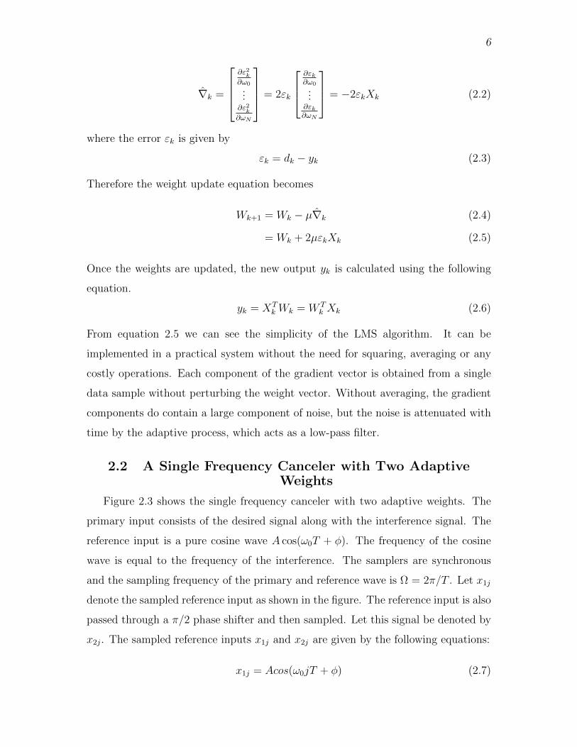
2.2 A Single Frequency Canceler with Two AdaptiveWeights
Figure 2.3 shows the single frequency canceler with two adaptive weights. The
primary input consists of the desired signal along with the interference signal. The
reference input is a pure cosine wave A cos(ω0T + φ). The frequency of the cosine
wave is equal to the frequency of the interference. The samplers are synchronous
and the sampling frequency of the primary and reference wave is Ω = 2π/T . Let x1j
denote the sampled reference input as shown in the figure. The reference input is also
passed through a π/2 phase shifter and then sampled. Let this signal be denoted by
x2j. The sampled reference inputs x1j and x2j are given by the following equations:
x1j = Acos(ω0jT + φ) (2.7)

7
x2j = Asin(ω0jT + φ) (2.8)
The equation for updating the weights as given by the LMS algorithm [7] are given
by the following equations:
ω1j+1 = ω1j + 2µεjx1j (2.9)
ω2j+1 = ω2j + 2µεjx2j (2.10)
Now, y1j and y2j are given by the following equations:
y1j = x1jω1j (2.11)
y2j = x2jω2j (2.12)
Therefore, yj as shown in Figure 2.3 is given by
yj = y1j + y2j (2.13)
With dj being the desired response, error signal εj is given by
εj = dj − yj (2.14)
Figure 2.4 shows the detailed operation of the circuit. The figure shows the signal
flow paths and aids in obtaining the transfer function of the circuit. The figure
also shows how the signal flow diagram is constructed based on equations defined
above. The weight update in the flow diagram is based on equations 2.9 and 2.10,
respectively. y1j and y2j are calculated in Figure 2.4 based on equations 2.11 and 2.12,
respectively. yj is obtained based on equation 2.13. Finally, the error signal εj is
calculated using equation 2.14. Let us assume that at time instant j = k, an impulse
of amplitude τ is applied at point C. Then we have,
εj = τδ(j − k) (2.15)
where
δ(j − k) =
1, for j = k0, for j 6= k
(2.16)
Then, the signal D and H at the output of the multipliers are given by:
εjx1j =
τA cos(ω0kT + φ), for j = k0, for j 6= k
(2.17)

8
εjx2j =
τA sin(ω0kT + φ), for j = k0, for j 6= k
(2.18)
The path from point D to point E and similarly from point H to point I represents a
digital integrator. The impulse response of this digital integrator is given by 2µu(j−
1), where u(j), is the unit step function given by:
u(j) =
1, for j ≥ 00, for j < k
(2.19)
The output at point ‘E’ ω1j is therefore obtained by convolving the impulse response
of the digital integrator 2µu(j − 1) with its input εjx1j.
ω1j = 2µτA cos(ω0kT + φ), for j ≥ k + 1 (2.20)
Similarly, the output at point I is obtained by convolving the impulse response of
the digital integrator 2µu(j − 1) with its inputs εjx2j.
ω2j = 2µτA sin(ω0kT + φ), for j ≥ k + 1 (2.21)
The signal at point ‘F’ and point ‘J’ at the output of the multipliers are given by:
y1j = 2µτA2 cos(ω0kT + φ) cos(ω0jT + φ), for j ≥ k + 1 (2.22)
y2j = 2µτA2 sin(ω0kT + φ) sin(ω0jT + φ), for j ≥ k + 1 (2.23)
The signal at point ‘G’ at the output of the summer is given by:
yj = 2µτA2 cos [(ω0jT + φ)− (ω0kT + φ)] , for j ≥ k + 1
= 2µτA2 cos [ω0T (j − k)] , for j ≥ k + 1 (2.24)
with τ = 1 and the time k set to zero, the signal at point G is given by
yj = 2µτA2 cos(ω0jT ),for j ≥ 1 (2.25)
which is the unit impulse response of the linear time-invariant system between point
‘C’ and point ‘G’ with the feedback loop from point ‘G’ to point ‘B’ open. The
transfer function of this system is
G(z) = 2µA2
[z(z − cos(ω0T ))
z2 − 2z cos(ω0T ) + 1− 1
](2.26)
=2µA2(z cos(ω0T )− 1)
z2 − 2z cos(ω0T ) + 1(2.27)

9
The transfer function in terms of the radian sampling frequency of Ω = 2π/T is given
by
G(z) =2µA2(z cos(2πω0Ω−1)− 1)
z2 − 2z cos(2πω0Ω−1) + 1(2.28)
The transfer function of the adaptive noise canceler from the primary input (point
‘A’) to the output (point ‘C’) with the feedback loop from point G to point B closed
is given by:
H(z) =z2 − 2z cos(2πω0Ω−1) + 1
z2 − 2(1− µA2)z cos(2πω0Ω−1) + 1− 2µA2(2.29)
The zeros of this transfer function are located at z =exp(+−i2πω0Ω−1). This implies
that the zeros are located on the unit circle at angles +i2πω0Ω−1 and −i2πω0Ω−1.
The poles are located at
z = (1− µA2) cos(2πω0Ω−1)+−i√
[(1− 2µA2)− (1− µA2) cos2(2πω0Ω−1)] (2.30)
This implies the poles are inside the unit circle at a radial distance of√
(1− 2µA2)
and at angles +− cos−1[(1 − µA2)
√(1− 2µA2) cos(2πω0Ω−1). For slow adaptation,
that is for small values of µA2, this value depends on
1− µA2√1− 2µA2
=
√√√√(1− 2µA2 + µ2A4
1− 2µA2
)(2.31)
∼= 1 (2.32)
This implies the angles of the poles is almost equal to the angles of the zeros.
Figure 2.5 illustrates the location of the poles and zeros. There are three inferences
that can be drawn from this figure
• The depth of the notch in the transfer function is infinite at the frequency
ω = ω0 since the zeros lie on the unit circle.
• For slow adaptation, the sharpness of the notch is high as corresponding poles
and zeros are separate by µA2.
• The notch bandwidth BW = µA2Ω/π as the distance between half-power
points is approximately 2µA2.

10
The Q of the notch is given by the ratio of the center frequency to the bandwidth
Q =ω0π
µA2Ω(2.33)
If more than one frequency is present in the reference input, a notch for each will be
formed as shown in [8].
Before we end this chapter, we wish to make the following observation. Adaptive
filters are time-varying systems by definition. We also know that transfer functions
can only be defined for linear and time invariant systems. Here, we still have a
transfer function for the single frequency canceler with two adaptive weights even
though it is a time variant system. Although this sounds like a paradox, there is a
reason for why the transfer function exists. Upon closer inspection of equation 2.24,
we observe that it is a only a function of (j − k). We see that it is proportional to
the input impulse defined in equation 2.15. Thus, equation 2.24 is a time-invariant
impulse response. Equation 2.24 turns out to be a function of only (j − k) since we
have a single frequency in our reference input.

11
ΣΣ
x0k
x1k
xNk
w0k
w1k
wNk
yk
Desired
Response
dk
Error
εk
+
+
+
+_
Input
Figure 2.1. The adaptive linear combiner
w0w1w* w2
Optimal
Weight
Initial
Guess
MSE, ξ
ξmin
Weight, w
Figure 2.2. Gradient search of univariable performance surface

12
Σ
ΣPrimary
Input
Reference
Input
π/2
Phase Shift2
LMS
Adaptation
Noise Canceler
Outputdj
x1j
x2j
w1j
w2j
yj
εj
A cos(w0t+Φ)
A sin(w0t+Φ)
The samplers are synchronous . Sampling Frequency Ω=2π/T rad/s.
x1j=A cos(w0jT+Φ) x2j=A sin(w0jT+Φ)
+
+
+
-
y1j
y2j
Figure 2.3. A single frequency canceler with two adaptive weights
Σ
Σ
-1
-1
2μ
2μ
X
X
X
X
cos(w0jT+ )
x2j=A sin(w0jT+ )
K L
F
M
H
J
Iw2j+1 w2j
Σ ΣG
dj
+
+
+_
εj C
A
yj
y1j
y2j
Equation 2.9
Equation 2.10Equation 2.13
Equation 2.11
Equation 2.12
εj
Equation 2.14
Figure 2.4. Signal flow paths of the single frequency canceler with two adaptiveweights

13
2πω0/Ω
ω=-ω0
ω=ω0
Half-power
points
x
x
Unit Circle
ω=0ω=Ω/2
Z-plane
Figure 2.5. The location of the poles and zeros

CHAPTER 3
CARRIER CANCELER CIRCUIT
In this chapter, we introduce the analog adaptive notch filter. We go over the
key differences of the analog adaptive notch filter compared to its equivalent digital
counterpart. We then introduce the block diagram of the carrier canceler and explain
its operation. We then explain how we obtain the schematic of the carrier canceler
from the block diagram of the circuit. The implementation of this schematic on a
Printed Circuit Board (PCB) did not work as expected and hence we present an
updated schematic. We go over the issues with the first implementation and how
they are solved in the second implementation.
3.1 Analog Adaptive Notch Filter
All the analysis above deals with the adaptive notch filter in the digital domain.
In the analog domain, the block diagram of the circuit is as shown in Figure 3.1.
As we can observe from Figure 3.1, the fundamental difference between the analog
and digital implementations of the circuit is the procedure in updating the adaptive
weights. The role of the accumulator between points D and E and points H and I
of Figure 2.4 is handled by the integrator in the analog version of the circuit. Also,
in the analog domain, the step size (µ) is equal to the time constant (λ) of the
integrator. Hence a relatively small time constant (λ) of the integrator will lead to
slow adaptation and all the results from the previous section regarding the digital
implementation of the notch filter can be readily extended to the analog version as
well.
3.2 Carrier Canceler
The schematic for the carrier canceler to be used in the TARA project is as shown
in Figure 3.2 .The signal from the receiver antenna acts as the primary input to the

15
circuit. A 54.1 MHz sine wave from a signal generator acts as the reference input to
the circuit. The adaptive loop combines the sine and the cosine signals to generate
a clean replica of the carrier. This replica of the carrier is then subtracted from
the received signal to remove the carrier signal from it. Figure 3.3 illustrates the
schematic and the components used in the first prototype of the circuit. AD835 is
a complete four-quadrant, voltage output analog multiplier. The output W of the
AD835 is related to its five inputs by the following equation
W = (X1−X2)(Y 1− Y 2) + Z (3.1)
An all-pass filter was implemented to introduce the necessary 90 degree phase shift to
the reference input. The schematic of an all-pass filter using an operational amplifier
is as shown in Figure 3.4.
At high frequencies, the capacitor is a short circuit, and therefore acts as a unity-
gain voltage buffer. At low frequencies, the capacitor is an open circuit and the circuit
acts as an inverting amplifier with unity gain. At the corner frequency ω = 1/RC of
the high-pass filter (f = 1/2π), Vout is 90 degrees out of phase from Vin.
At high frequencies, the circuit acts as a unity-gain voltage buffer. At low
frequencies, the circuit acts as an inverting amplifier with unity gain. At the corner
frequency of the high-pass filter the output of the all-pass filter is 90 degrees out of
phase from its input. LMH6654 was used for implementing the integrators and the
differential amplifier. Due to the imperfections of amplifiers at high frequencies and
due to the fact that the amplifiers which are available and that suite our application
have a high noise figure, the differential amplifier was replaced by a directional coupler
in the second prototype. Figure 3.5 illustrates the schematic and the components
used in the second prototype of the circuit.

16
X
X
∫
X
X
∫
Σ Σ
Primary Input
Error/Output
cos(wct)
sin(wct)
LMS Adaptation
+
+
+_Reference
Pair
Figure 3.1. Block diagram of the analog adaptive notch filter
X
X
∫
X
X
∫
Σ Σ
Antenna Input
Error/Output
cos(wct)
sin(wct)
LMS Adaptation
+
+
+_Reference
Pair
(54.1MHz)
Figure 3.2. Block diagram of the carrier canceler

17
Carrier
Reference
Analog
Multiplier(AD835)
Analog
Multiplier(AD835)
All-Pass
Filter(LMH6654)
Integrator(LMH6654)
Analog
Multiplier(AD835)
Analog
Multiplier(AD835)
Integrator(LMH6654)
Differential
Amplifier(LMH6654)
Signal from
antenna
Carrier Canceler
Output
A cos(w0t+Φ)
A cos(w0t+Φ)
A sin(w0t+Φ)
A sin(w0t+Φ)
Figure 3.3. Schematic and the components used in the first prototype of the circuit
Figure 3.4. Schematic of an all-pass filter

18
Carrier
Reference
Analog
Multiplier(AD835)
Analog
Multiplier(AD835)
All-Pass
Filter(LMH6654)
Integrator(OPA171)
Analog
Multiplier(AD835)
Analog
Multiplier(AD835)
Integrator(OPA171)
Directional
Coupler
Signal from
antenna
Carrier Canceler
Output
A cos(w0t+Φ)
A cos(w0t+Φ)
A sin(w0t+Φ)
A sin(w0t+Φ)
Figure 3.5. Schematic and the components used in the second prototype of thecircuit

CHAPTER 4
CHALLENGES FACED
In the previous chapter we suggested a block diagram for implementing the carrier
canceler circuit, as shown in Figure 3.5. As with any analog circuit, there were some
issues encountered when implementing the circuit on a PCB. It turns out that a
straight forward implementation (Figure 3.5) into a circuit will lead to the circuit
not attenuating the carrier at all. In-fact the carrier seemed to be amplified by 2-3
dB in some cases. It turns out that the reason for such strange behavior is due to
the fact that the circuit had positive feedback instead of negative feedback. The
propagation delay of each component in the circuit led to the circuit having positive
feedback.
Even with the problem of positive feedback resolved, the circuit was not attenu-
ating the carrier by a reasonable amount. The carrier seemed to be attenuated by
not more than around 10 dB. After a lot of debugging the circuit, the reason for this
behavior was attributed to the DC offset at the output of the multipliers used in the
circuit. The analog multipliers used in the circuit have a DC offset of around 35 - 40
mV. This caused the circuit to attenuate the carrier by a small amount. The reason
for doing so is explained further in this chapter.
Section 4.1 of this chapter concentrates on the problem of positive feedback in
the circuit. We also propose solutions to overcome this problem. Section 4.2 of this
chapter explains the problem of DC offset of the multipliers. It also explains why the
problem of DC offset is so significant in our circuit. Also, a solution for overcoming
the problem of DC offset is proposed.
4.1 Phase Shift
The circuit is designed based on ideal mathematical modeling of the circuit
components and relies on negative feedback. Each IC component used in the circuit

20
has an inherent delay associated with it. This delay accounts to a phase shift over
a narrow band. Due to the phase shift of all the components, the original circuit
designed to have a negative feedback ended up having a positive feedback instead.
Additional circuitry had to be incorporated around the analog multiplier (AD 835)
to overcome this problem. The functional block diagram of AD 835 is as shown in
Figure 4.1. The circuit has 5 inputs X1,X2,Y 1,Y 2 and Z. The circuit has 1 output
W . The output is W = XY + Z, where X = X1 − X2 and Y = Y 1 − Y 2. If a
cosine wave cos(ω0T ) is fed into the input X1 and a sine wave sin(ω0T ) is fed into the
input Y 1, with X2 and Y 2 grounded, the output W = 1/2 sin(2ω0T ) is as shown in
Figure 4.2. If the entire circuit has a positive feedback, a 180 degree phase shift can
be introduced at the output of the multiplier by feeding the cosine wave cos(ω0T )
into the input X2 and grounding X1, as shown in Figure 4.3. Figures 4.4 and 4.5
show a configuration by which this can be achieved. By having R1,R4,R5 and R8 in
place, a 180 degree phase shift can be achieved compared to having R2,R3,R5 and
R8 in place.
4.2 DC Offset
The problem of DC offset was the most difficult to identify at first. The carrier
canceler circuit would attenuate the carrier signal by around 5dB and then the output
would stay constant. It would show no signs of trying to cancel the carrier further.
This was very puzzling at first. After trying to debug various parts of the circuit that
would lead to this behavior, we happened to measure the DC voltage at the output
of the multiplier. The multiplier, when powered on, has a DC voltage of around
35 mV at its output. This DC offset voltage would be insignificant in almost all
scenarios. However, since the output of two of the multipliers are the inputs of two
integrators, this DC offset voltage is very significant. If this DC offset voltage is not
canceled, the integrators would continuously integrate this voltage and ultimately
reach saturation. In order to prevent the integrators from reaching saturation, the
circuit tries to cancel this DC offset voltage. The circuit tries to produce a sinusoid
at the output, which would lead to a DC voltage that is equal in magnitude and
opposite in sign when multiplied with the reference input. Hence, the output of the

21
circuit can never truly go to zero.
This problem of DC offset was overcome by applying a voltage that is equal to
the DC offset voltage of the multiplier, to the noninverting input of the op-amp used
in the integrator circuit. A potentiometer was used for this purpose to fine tune the
voltage applied to the noninverting input so as to achieve maximum cancellation of
the carrier.

22
Σ+
+
X1
X2
Y1
Y2
X = X1 - X2
Y = Y1 - Y2
XY XY + ZX1 W OUTPUT
Z INPUT
+
+
Figure 4.1. Functional diagram of AD835
AD 835
X1
X2
Y1
Y2
W
cos( 0T)
sin( 0T)0.5sin(2 0T)
Figure 4.2. AD835 with two sinusoidal inputs

23
AD 835
X1
X2
Y1
Y2
W
cos( 0T)
sin( 0T)-0.5sin(2 0T)
Figure 4.3. AD835 with 180 degree phase shift
AD 835
X1
X2
Y1
Y2
W
R1
R2
R3
R4
R5
R6
R7
R8
cos( 0T)
sin( 0T)
0.5sin(2 0T)
Figure 4.4. Practical implementation of Figure 4.2

24
AD 835
X1
X2
Y1
Y2
W
R1
R2
R3
R4
R5
R6
R7
R8
cos( 0T)
sin( 0T)
-0.5sin(2 0T)
Figure 4.5. Practical implementation of Figure 4.3

CHAPTER 5
CIRCUIT SIMULATION
In order to better understand the behavior of the carrier canceler circuit and
to make better informed decisions on modifying the circuit, CAD simulations of
the circuit are performed. A parametric model of the circuit is obtained by direct
measurement of the behavior of each component in the circuit. Since the circuit is
designed to operate at the carrier frequency of 54.1 MHz, the propagation delay of
each IC results in a phase shift over a narrow passband. This phase shift is measured
and added to the simulation. The analog multipliers used in the circuit have a DC
offset. Hence a DC offset is also added at the output of each multiplier to model its
observed behavior. Also, each component has a specific gain that is measured and
added to the simulation model. This section presents the results of the simulation.
Specifically, we have a look at the effects of the components phase shift, multipliers
output DC offset, and the frequency offset between reference input and antenna
input, on output signal level.
5.1 Phase Shift
In the first simulation, we have a look at just the effect of phase shift of all the
components on output signal level. Here the phase shift for all the components were
included, with the multipliers output DC offset and frequency offset set to zero. The
reference input level is set to 400 mV and the antenna input level is set to 10 dBm.
Negative feedback is obtained by implementing the techniques discussed in section
4.1. Simulation results show that the circuit works perfectly in negative feedback
mode and the output signal level is continuously decreasing. This shows that if the
total phase shift of the circuit is compensated properly to maintain negative feedback,
complete carrier rejection occurs.

26
5.2 DC Offset
In the second simulation, we have a look at the effect of the DC offset of the
multipliers while maintaining the actual values of the components phase shifts and
frequency offset set to zero. The DC offset of the multipliers is set to 50 µV .
Figure 5.1 shows the simulation result for the output signal level in this case when
compared to the output signal level when the DC offset is set equal to zero. Note
that the output signal level when DC offset exists is limited to −45 dBm. This
output signal residual level can be calculated using:
Verror =Voffset
Vref
=50× 10−6
400× 10−3= 1.25 mV (5.1)
Assuming a 50 Ω load, output signal level will be −45 dBm, which is consistent with
the simulation results.
5.3 Frequency Offset
In the third simulation, we have a look at the effect of frequency offset between
reference and antenna input on the output signal level. The antenna input frequency
offset was set equal to 10 Hz, while also including DC offset of the multipliers and
maintaining the actual values of the components phase shifts. The output signal
level is shown in Figure 5.2. We observe that the output signal level is oscillating
with a frequency of 10 Hz and this is equal to the offset frequency.
In addition, we observe that the minimum output signal level is higher, compared
to the simulation results with zero frequency offset. This means, as one would
expect, any frequency offset between the carrier signal and the reference input leads
to performance degradation of the circuit. This high sensitivity of the circuit to
an offset between the reference input and the carrier at the antenna input can be
attributed to the very narrow bandwidth (e.g., 300 Hz) of the circuit. This problem
can be overcome if the reference input is directly extracted from the antenna input.
This can be achieved effectively by feeding the antenna input to a phase locked
loop (PLL) circuit to generate a sine wave whose frequency exactly matches the
carrier frequency. This addition also makes the carrier canceler circuit adaptive to
variations of the carrier frequency, as long as it remains within the lock range of the

27
PLL circuit. This is not implemented in the current system but can be implemented
in future systems to overcome the problem of frequency offset.

28
0 2 4 6 8 10−100
−80
−60
−40
−20
0
dB
m
Time (mSec)
Zero DC Offset
With DC Offset
Figure 5.1. Simulation: Output signal level for zero DC offset and 50 µV DC offset
0 100 200 300 400 500−50
−40
−30
−20
−10
0
dB
m
Time (mSec)
Figure 5.2. Simulation: Output signal level for 50 µV DC offset and 10 Hz frequencyoffset

CHAPTER 6
RESULTS
The carrier canceler circuit was tested in the lab first to ensure its correct
operation and then it was tested in the receiver station at Longridge. The following
sections describe the results obtained in detail.
6.1 Laboratory Test Results
The carrier canceler circuit was tested and debugged in the laboratory until
satisfactory performance was achieved. The first experimental setup to verify the
correct operation of the carrier canceler circuit was as follows. The antenna input
and the reference input were fed by the same 3dBm sinusoidal signal at 54.1 MHz
from a signal generator. The output was connected to an NI-5761 digitizer module
(16 bit ADC, 250 MSample/sec), and was recorded by an NI-7965R FPGA module,
to see if the carrier level at the output was lesser than the input. The output with this
setup, with the potentiometers tuned to cancel the DC offset and achieve maximum
attenuation is as shown in Figure 6.1
As seen in Figure 6.1, the output of the circuit is more than 50dB below the input.
This proves the correct operation of the circuit. The next setup to verify the correct
operation of the circuit involved adding a chirp signal to the carrier, at the antenna
input. To verify that the circuit was functioning correctly, the chirp signal should be
unaltered by the circuit while still attenuating the carrier signal. The antenna input
was fed with a +3 dBm signal at frequency 54.1 MHz, which is combined with a 50
dB weaker wide-band chirp signal that spans from 30 MHz to 70 MHz. The reference
input is fed with 400 mV, 54.1 MHz signal from a signal generator. Figure 6.2 shows
the the spectra of the antenna input and the carrier canceler output.
As seen in Figure 6.2, the carrier signal is attenuated by more than 50 dB, while
the wideband chirp signal is left unaffected. This shows that the carrier canceler

30
attenuates the frequency of the reference input and leaves the rest of the spectrum
untouched.
6.2 Field Test Results
The next step in the verification of the carrier canceler circuit was to test its
correct operation in the field. The carrier canceler circuit was installed at the TARA
receiver site. The signal from the antenna passes through a bank of filters and
amplifiers. The filter bank includes an RF limiter, broad band amplifier, low pass
filter, high pass filter and an FM band stop filter as described in [2]. The received
signal contains a −21 dBm signal at frequency 54.1 MHz, which is 50 dB higher
than the background noise. This received signal is fed to the antenna input of the
carrier canceler circuit. The reference input is fed with 0 dBm tone at 54.1 MHz
from a signal generator. Signal generator frequency is tuned to match the received
signal frequency, and potentiometers are tuned to compensate output DC offset of
multipliers and achieve maximum attenuation. The results of this experiment are
presented in Figure 6.3. As seen, the field test results are similar to those of the lab
test. The carrier can be removed almost perfectly, by tuning the reference input to
match the carrier at the primary input.
As seen in the plots in section 6.1 and section 6.2, the carrier canceler circuit has
introduced some broadband background noise into the output. The reason for this
is explained in section 7.2.

31
0 20 40 60 80 100 120−100
−80
−60
−40
−20
0
20
X: 54.1
Y: 2.986
MHz
dB
m
X: 54.1
Y: −49
Output
Antenna Input
Figure 6.1. Carrier canceler with an attenuation of more than 50 dB
0 20 40 60 80 100−100
−80
−60
−40
−20
0
20
X: 54.1
Y: 2.957
dB
m
MHz
X: 54.1
Y: −50.61
Output
Antenna Input
Figure 6.2. Lab test: Spectra of antenna input and carrier canceler output

32
0 20 40 60 80 100−100
−80
−60
−40
−20
0
X: 54.1
Y: −63.49
MHz
dB
m
X: 54.1
Y: −21.4
Output
Antenna Input
Figure 6.3. Field test: Spectra of antenna input and carrier canceler output

CHAPTER 7
CONCLUSION AND FUTURE WORK
This chapter summarizes the main findings in this thesis and outlines the work
to be done in the future.
7.1 Conclusion
This thesis showed the design and implementation of an analog adaptive notch
filter. The notch filter was designed to remove a 54.1 MHz carrier signal, which
is used for detection of cosmic air showers in the The Telescope Array RAdar
(TARA) project. The thesis involved designing a 4-layer PCB which consisted of
surface mount components. The circuit used the LMS algorithm to achieve carrier
cancellation. The circuit was designed to have a flat gain from 30 MHz to 100
MHz. Stability issues arose due to the time delay of the ICs. The circuit, which was
originally designed to have a negative feedback, ended up having a positive feedback
due to the time delay of the ICs. Hence, additional circuitry had to be incorporated
to maintain negative feedback in the circuit. DC offset of the multipliers used in
the circuit caused performance degradation. Hence, additional circuitry had to be
included which nullified the effect of the DC offset of the multipliers. The final
design with all these additional circuitry incorporated was first tested in the lab and
then tested at the receiver station of the TARA project at Longridge. The circuit
achieved carrier attenuation of 45 dB or better. The 3 dB bandwidth of the circuit
was measured and found to be 300 Hz.
7.2 Future Work
As noted in section 4.2, the problem of DC offset of the multipliers is currently
rectified by tuning potentiometers to compensate for the offset and achieve maximum
cancellation. This solution requires the potentiometers to be tuned manually. If

34
the circuit is intended for use in the field, then an automatic way of tuning the
potentiometers is preferable. This would require a microcontroller which would
calibrate tune-able potentiometers to achieve maximum cancellation.
As seen in Figure 6.1, the carrier canceler circuit has introduced some broadband
background noise into the output. Inspection of Figure 6.3 also reveals that the
carrier canceler circuit has introduced background noise into the output. This noise
originates from the AD835 multipliers, which have an output noise of −133 dBm/Hz,
according to their datasheet. We also notice that the background noise in Figure 6.3
seems to be more pronounced. This is partly because at the field there was no
chirp signal and the original background noise in the field is lower compared to
the laboratory experiment. Hence, the noise produced by the analog multipliers
dominates the original background noise in the field, since it is higher in magnitude.
This problem, although unresolved in the present design, can be resolved by imple-
menting a band-pass filter before the directional coupler. The replica of the carrier
generated by the circuit should pass through the band-pass filter, before being fed
to the directional coupler. The band-pass filter should be designed to pass a narrow
band of frequencies centered at 54.1 MHz to remove any noise generated by the
analog multipliers.

REFERENCES
[1] “Telescope array radar project.” [Online]. Available: http://www.telescopearray.org/tara/
[2] R. Abbasi, M. A. B. Othman, C. Allen, L. Beard, J. Belz, D. Besson, M. Byrne,B. Farhang-Boroujeny, A. Gardner, W. Gillman, W. Hanlon, J. Hanson,C. Jayanthmurthy, S. Kunwar, S. Larson, I. Myers, S. Prohira, K. Ratzlaff,P. Sokolsky, H. Takai, G. Thomson, and D. V. Maluski, “Telescope array radar(tara) observatory for ultra-high energy cosmic rays,” Nuclear Instruments andMethods in Physics Research Section A: Accelerators, Spectrometers, Detectorsand Associated Equipment, vol. 767, no. 0, pp. 322 – 338, 2014. [Online]. Available:http://www.sciencedirect.com/science/article/pii/S0168900214009358
[3] B. Widrow, J. Glover, J.R., J. McCool, J. Kaunitz, C. Williams, R. Hearn, J. Zei-dler, J. Eugene Dong, and R. Goodlin, “Adaptive noise cancelling: Principles andapplications,” Proceedings of the IEEE, vol. 63, no. 12, pp. 1692–1716, Dec 1975.
[4] T. Kwan and K. Martin, “An adaptive analog continuous-time cmos biquadraticfilter,” Solid-State Circuits, IEEE Journal of, vol. 26, no. 6, pp. 859–867, Jun1991.
[5] T. Linder, H. Zojer, and B. Seger, “Fully analogue lms adaptive notch filter inbicmos technology,” Solid-State Circuits, IEEE Journal of, vol. 31, no. 1, pp.61–69, Jan 1996.
[6] D. Frey and L. Steigerwald, “An adaptive analog notch filter using log filtering,”in Circuits and Systems, 1996. ISCAS ’96, Connecting the World, 1996 IEEEInternational Symposium on, vol. 1, May 1996, pp. 297–300 vol.1.
[7] B. Farhang-Boroujeny, Adaptive Filters: Theory and applications, 2nd Edition.John Wiley and Sons, 2013.
[8] J. R. Glover, Adaptive noise cancelling of sinusoidal interferences, Ph.D. Disser-tation. Dept. of Electrical Engineering, Stanford University, Stanford, California,1975.