analog hardware description language a thesis the
TRANSCRIPT

ANALOG HARDWARE DESCRIPTION LANGUAGE
FOR A RADIO FREQUENCY SYSTEM
by
SAMSOO KANG, B.S., M.S., Ph.D.
A THESIS
IN
ELECTRICAL ENGINEERING
Submitted to the Graduate Faculty of Texas Tech University in
Partial Fulfillment of the Requirements for
the Degree of
MASTER OF SCIENCE
IN
ELECTRICAL ENGINEERING
Approved
Chairperson of the Committee
Accepted
Fhterim Dean of the Graduate Scb^oK
December, 2000

ACKNOWLEDGEMENTS
I would Hke to thank my research advisor. Dr. Micheal E. Parten, for his patient
and helpful guidance during this research and the preparation of this thesis. I thank Dr.
Sunanda Mitra for serving as my committee member. I thank Ms. Shu Yang for
solving my computer-related problems. I am grateful to the Department of Physics,
Texas Tech University, for financial support in the form of teaching assistantships. I
thank my mother, mother-in-law, and my family and friends in Korea for their
heartfelt support. I also thank my son, David for just being my son. Finally, I thank my
wife, Heykyoung, for her heartfelt love and encouragement, which made this work
possible.
11

CONTENTS
ACKNOWLEDGEMENTS ii
LIST OF FIGURES v
CHAPTER
I. INTRODUCTION 1
II. THEORETICAL BACKGROUND 5
2.1 Circuit Simulation 5
2.2 Analog Hardware Description Language 15
2.3 Analog Operators in Verilog-AMS 15
2.4 Analog System using Verilog-AMS 18
2.4.1 Time Derivative Operator 20
2.4.2. Time Integral Operator 22
2.4.3 Linear Time Delay 22
2.4.4 Transition Filter 23
2.4.5 Slew Filter 24
2.4.6 Laplace transform filter 24
2.4.7 Z-Transform filter 26
III. DOWN CONVERTER 27
3.1 Basic Concepts in RF Design 28
3.1.1 Input/Output Matching 29
3.1.2 Conversion Gain 30
111

3.1.3 Nonlinearity 31
3.1.4 Noise 34
3.1.5 Noise Factor 40
3.1.6 Low Noise Amp. 41
3.1.7 Mixer 47
3.1.8 Intermediate Frequency (IF) Amp. 52
3.1.9 Band Pass Filter 53
rV. RESULTS 58
4.1 Now Noise Amplifier 58
4.2 Mixer 63
4.3 IFAMP 70
4.4 Band Pass Filter 71
V. CONCLUSIONS 79
REFERENCES 82
IV

LIST OF FIGURES
2.1 Standard procedure of IC production 7
2.2 Schematic of a CMOS OP AMP 11
2.3 Macromodel of a CMOS OP AMP 12
2.4 Verilog-AMS code of a CMOS OPAMP 16
2.5 General potential and flow direction 21
3.1 Block diagram of a downconverter 29
3.2 CPl definition 35
3.3 IPn definition 36
3.4 Schematic diagram of a low noise amplifier 44
3.5 Input stage of LNA 45
3.6 Input equivalent circuit of LNA 45
3.7 Schematic of LNA output stage 48
3.8 Equivalent circuit for Figure 3.7 48
3.9 Schematic diagram of a mixer 51
3.10 Schematic diagram of an IF amplifier 54
3.11 Equivalent block diagram of IF AMP 55
3.12 Schematic diagram of a band pass filter 57
4.1 AC Response for Schematic and VerilogA Results in LNA 61
4.2 Noise Currents in LNA 64
4.3 VerilogA Code for LNA Simulation 65
4.4 Conversion Gain for Schematic and VerilogA in Mixer 67
4.5 Noise Currents in Mixer 68
4.6 Input Third-Order Intercept Point for Schematic in Mixer 69
4.7 VerilogA code for Mixer Simulation 72
4.8 AC Response for Schematic and VerilogA Simulation in IFAMP 73
4.9 Noise Simulation for Schematic and Verilog in IFAMP 74
4.10 VerilogA code for IFAMP simulation 75
4.11 AC Response for Schematic and VerilogA in Band Pass Filter 77
4.12 VerilogA Code for BPF Simulation 78
VI

CHAPTER I
INTRODUCTION
Since the SPICE [1,2] simulator was developed at Berkeley, it has been used for
the final prefabrication verification of the detailed electrical behavior of integrated
circuits and has provided accurate results. However, for complex analog or mixed
signal systems, accurate circuit simulation of the entire circuit is out of question. For
example, in a phase-lock loop (PLL) in a radio-frequency (RF) receiver, the period of
the voltage-controlled oscillator (VCO) is much smaller than the loop time constant.
Thus the simulator has to go many cycles to get an idea of the behavior of the circuit.
This takes more memory and simulation time and makes SPICE simulation
impractical for widely separated timing events or time constants.
In order to solve this problem, several approaches have been taken. One of them is
macro modeling or behavioral modeling. This method uses a block as a device, which
has a predefined circuit primitive. Once a block has been designed, it is then verified
for its expected functionality in the system. This can be a device, like a transistor, or
many of these devices. Thus, this is a top-down design rather than bottom-up design.

This behavioral modeling can reduce the simulation time but has less accuracy, thus
there is a trade-off between accuracy and the complexity.
There are several simulators to implement both conventional simulation and
behavioral modeling. These are "Analog Multi-Level Simulators" such as PSPICE
(MicroSim), HSPICE (MetaSoftware), SABER (Analogy), and SPECTRE (Cadence).
Behavioral models are described in terms of s or z domain transfer function,
differential equations, C code or Analog Hardware Description Language (AHDL) [3].
Many people and many companies are involved in developing AHDLs [3]. The
MIMIC HDL (MHDL) is intended to address the domain of analog and microwave
hardware [4]. The extending of VHDL and Verilog to support analog circuits are being
developed and are called VHDL-AMS (formeriy VHDL-A) [5] and Verilog-A
(formerly Verilog-A) [6] respectively. For mechanical systems, as well as the electrical
systems, MAST from Analogy [7] is used together with the simulator SABER. The
University of Cincinnati has used AnaVHDL to simulate mixed-signal circuits. Other
commercial software, which come with AHDLs are PSPICE and SPECTRE-HDL
(Cadence).
Most of the AHDL simulators described above are considered as "Analog Multi-
Level Simulators." These can do high performance analog and mixed signal

simulation and also provide full support to represent analog second-order effects such
as noise, distortion and statistical variations. These "Analog Multi-Level" simulators
are convenient extensions to the traditional macro modeling approach. A model of a
comparator using AHDLs has been shown to be equivalent to traditional macro
modeling with basic circuit primitives [8].
The biggest advantage of using AHLDs is low simulation cost. Once the
specifications are set, AHLDs can implement them directly without any circuits, logic,
or device parameters. It is just like writing a computer language such as C+-i- or Java.
Also, the iteration time is tremendously reduced. Circuit designers who use
conventional methods have to develop the circuit device including parameters. For
large circuits, this development can take an enormous amount of time. Modifications
of the circuit can be very difficult.
The purpose of this thesis is to investigate the possibility of using AHLDs for
applications in implementing a top-down design methodology. A good example of this
is an electrical system, specifically a receiver in an RF system. This particular circuit
was chosen because it is a good representation of a circuit that contains an adequate
amount of circuitry with enough complexity for a first attempt to develop a behavioral
model of a system level circuit. Verilog-AMS was used to simulate the RF receiver

circuit and the Cadence design system, especially SpectreS along with Analog Artist,
was used to implement the Verilog-AMS code. This is capable of behavioral modeling
as well as the total control of the conventional simulation models. In order to simulate
both schematics and Verilog-AMS blocks, general purpose-building blocks are used as
in digital simulation. Cell libraries are used in digital hardware description languages.
For this analogy, broadband amplifiers are chosen. In this thesis the circuit simulation
for a down converter in a receiver circuit by the conventional and the Verilog-AMS
were accomplished and compared.
The remainder of this thesis is organized as follows. Chapter II reviews the
background of the Analog Hardware Description Language, especially Verilog-AMS
including a brief history of the earlier applications. As the application of this thesis, a
down converter is discussed in Chapter III. In this chapter the theory, background, and
a brief history are discussed. Also the simulation results using SpectreS are shown.
Next Chapter IV discusses the results using Verilog-AMS. Various simulation results
such as gain, noise, and IIP3 are shown for several sub-blocks. These results are
compared to the results in chapter III. Chapter V summarizes the results and contains a
discussion.
CHAPTER II
THEORETICAL BACKGROUND
2.1 Circuit Simulation
The analog integrated circuit (IC) product cycle has many steps from the
specification to the final product as shown in Figure 2.1. A specification is used to
qualify the design of an IC. Various simulators are used to check the initial operations.
After finishing the layout, final verification of the IC is completed and verified against
the extracted layout design database. The design is subjected to test after fabrication of
the IC. From the initial specification, design, simulation, layout, verification, and test
are iterated until the specification is satisfied.
SPICE is the most popular circuit simulator these days. A circuit netlist is used to
describe the connectivity of the components. All components, such as resistors,
inductors, and transistors have device models. These models can be extracted from the
semiconductor processes and are used for SPICE together with controlled sources.
These models play important roles in the simulation because the model is the basis of
the accuracy. The accuracy and complexity of the models are changing continuously.
The circuit is simulated either in the time domain or the frequency domain. The set of

differential equations are solved in a time domain simulation. Figure 2.2 shows a
circuit for a simple opamp. A typical SPICE model for this opamp is shown below.
* EXAMPLE OPAMP SPICE SIMULATION
VDD VDD 0 5V
VIN INPUT 0 DC 5V PULSE (0 5V 0 INS INS 20US 40US)
Ml VDD OUTPUT OUTPUT VDD PMOD L=1U W=20U
M2 VDD VB3 OUTPUT VDD PMOD L=1U W=20U
M3 VDD VB3 2 VDD PMOD L=1U W=20U
M4 VDD 2 2 VDD PMOD L=1U W=20U
M5 OUTPUT VB2 3 GND NMOD L=1U W=20U
M6 2 VB2 4 GND NMOD L=1U W=20U
M7 3 INPUT 1 GND NMOD L=1U W=20U

Design Concept
Specification
Figure 2.1 Standard procedure of IC production

M8 4 GND 1 GND NMOD L=1U W=20U
M9 1 VBl GND GND NMOD L=1U W=20U
.MODEL NMOD NMOS (VT0=1 KP=4.5E-5 CBD=5PF CBS=2PF RD=5
+ RS=2 RB=0 RG=0 RDS=1MEG CGSO=lPF CGBO=lPF)
.MODEL PMOD PMOS (VTO=-l KP=4.5E-5 CBD=5PF CBS=2PF
+ RD=5 RS=2 RB=0 RG=0 RDS=1MEG CGSO=lPF CGBO=lPF)
*
.TRAN lUS 80US
.TF V(OUTPUT) VIN
.OP
.PLOT TRAN V(OUTPUT) V(VIN)
.PROBE
.END
8

In frequency domain simulation, the circuit can be linearized at the operating point
then linear equations are solved as functions of frequencies. Due to this linearization
within the small region, SPICE may not be used for complex systems because the
simulation time is estimated 0(/t'^ ) , where n is the number of nodes in the system
[8].
One type of modeling to solve this long simulation time is marco modehng [9-13].
This macro modeling involves predefined SPICE primitives, such as voltage controlled
voltage sources, voltage controlled current sources, resistors, and capacitors. For
example, the operational amplifier (opamp) circuit shown in Figure 2.2 is modeled by
the macromodel [14] shown in Figure 2.3. Nine transistors in the opamp circuits are
represented using a non-linear controlled current source, a voltage source, a resistor,
and a capacitor. The non-linear controlled current source, gml is well known as the
transconductance of the non-linear input differential pair. The DC voltage source sets
the DC output bias voltage. The resistor, rim, and the capacitor, dm, represent the
output resistance and the output capacitance at the output node, respectively. The
listing of the simulation file follows.

EXAMPLE OPAMP MACROMODELING
VIN INPUT 0 DC 5V PULSE (0 5V 0 INS INS 20US 40US)
GMl OUTPUT GND INPUT GND 5.9E-9
EC 1 GND OUTPUT GND 1
RLM OUTPUT 1 45
CLM OUTPUT GND 3.0E-11
.TRAN lUS SOUS
.TF V(OUTPUT) VESf
.OP
.PLOT TRAN V(OUTPUT) V(VIN)
.PROBE
.END
For specific types of circuits, for example, opamps by Boyle et al. [10],
comparators by Getrreu et al. [9], and phase-locked loops by Tan [13], manually
tuned macromodels are available. They tuned these macromodels manually to
minimize the error. These macromodels can not be controlled and the qualities are
10

a
Vin gm1 \ / :
/ ! N ^ 1
\ v i / / \ V /
rim
^-0
Vout <
dm
\
[ n
Figure 2.2 Schematic of a CMOS OPAMP
11

Figure 2.3 Macromodel of a CMOS OPAMP
12

are not very high. On the other hand, Casinovi et al [14] used a general-purpose
rigorous algorithm to solve the minimum-maximum problem, to find the optimal
macromodel. This is an extension of the Hamiltonian formulation of a classical optimal
control problem. Thus, the accuracy of the macromodel can be qualified and controlled.
PSPICE [11] and HSPICE [12] include macromodeling. The "Analog Behavioral
Modeling" (macromodeling) option in PSPICE allows the designer to use more flexible
descriptions for electric components in terms of a transfer functions. HSPICE offers a
higher level of abstraction and a speed up over the lower level description of an analog
function. All elements including nodal voltages, element currents, time, and user-
defined parameters, such as voltage or current sources, can be described by functions.
Other commercial simulators, which can perform macromodeling, are SABER [15]
and iMACSIM [16]. SABER uses the MAST language as input. MAST allows the
circuit to use templates to describe the component's behavior using differential
equations and equations relating time of events. Each node satisfies both Kirchoff's
voltage law (KVL) and Kirchoff's current law (KCL). The difference between this
method and traditional macromodeling is that a template is defined by a set of
differential equations while a macromodel is defined by a network of basic components.
In iMACSIM, circuit blocks can be described in terms of s-domain or z-domain transfer
13

functions and their interaction described using signal flow diagrams that includes
summers, multipliers, etc. Macromodels written in "C" are allowed.
However, this has several disadvantages too. First, once the macromodel is defined,
the output response for a specific input waveform is optimized. When different
responses are modeled for new input conditions, the accuracy of the macromodel is not
guaranteed. Second, great expertise is needed to devise a macromodel. Otherwise the
simulation time reduction is very small. Third, there are very few tools for extracting
parameters for macromodels even though Casinovi et al. [14] proposed a methodology
for automatic macromodel construction and Ma et al. [17] presented model generation
and validation tools for iMACSIM. Fourth, since the macromodels are deterministic and
focus on time domain circuit behavior, it is very difficult to simulate frequency domain
effects, noise effects, and effects due to process variations.
Even though there are special purpose simulators such as SWITCAP [18] for
switched capacitor networks and MIDAS [19] for mixed-mode sampled-data systems
and these can handle frequency domain and noise simulations, it is very hard to find a
general-purpose macromodel simulator specifically to simulate process variations. This
needs a new type of simulator, analog hardware description language.
14

2.2 Analog Hardware Description Language
An analog hardware description language (HDL) is a programming language, which
is designed to allow the modeling of hardware that performs a continuous-time function.
Figure 2.4 shows a simple HDL box for an opamp shown in Figure 2.2. As seen in
Figure 2.4, the direction for a potential is indicated by plus and minus symbols at each
end of the branch. Voltage at the plus sign is higher than voltage at the minus sign. For
an electrical device, in the Verilog-AMS language, voltage would be represented by
V(p,n), and the associated current flow would be represented by I(p,n).
2.3 Analog Operators in Verilog-AMS
One of the advantages of Verilog-AMS is that the data type and statement are
similar to the fundamental concept of modeling in mathematics. For example, if
someone needs an analysis for only the frequency of response of a system, then the
adequate HDL model would be a transfer function of the appropriate complexity. A
more specific example of modeling instead of using complicated resistor, transistor, and
capacitor SPICE models, is a mathematical description or behavioral expression, which
describes the component electrically. Together with an appropriate simulator.
15

INPUT
// Verilog-A example for an opamp
module opamp (input, output);
inout input, output;
electrical input, output;
parameter gain = le8;
analog begin
V(output) <+ -gain * V(input);
End
endmodule
Figure 2.4 Verilog-AMS code of a CMOS OPAMP
16

analog HDL can model any system that can be described with nonlinear, ordinary
differential equations (ODEs). In all technologies, there are fundamental laws that are
enforced by the simulators, regardless of technology or complexity. Such laws are
Kirchoff's current law (KCL) and Kirchoff's voltage law (KVL).
For electrical circuits, KCL is enforced by the simulator in the process of finding a
valid solution to the system of equations. For this, analog HDL provides the concept of
through and across variables, which are used by the simulator as the dependent and
independent variables of ODE at a node. Electrical current, dissipative power, and
hydraulic flow are through variables. These variables at the nodes, are summed to zero
by the simulators. The across variables, such as electrical voltage, temperature, and
hydraulic pressure are typically taken as the independent variable that the simulator
iteratively refines from the initial guess to solve the system equations.
VHDL-AMS and Verilog-AMS are the main hardware description languages to
model electrical circuits. VHDL-AMS, also known as IEEE1076.1 is a major effort to
extend VHDL for the description and the simulation of analog and mixed-signal circuits
and systems. The VHDL-AMS language has been designed within the 1076.1 Working
Group of Design Automation Standards of Committee of the IEEE Computer Society.
17

The Verilog-AMS language, the result of two year process of development and the
standardization through Open Verilog International (OVI) and now continuing through
IEEE, extends the syntax and and semantics of the Verilog HDL language for the
description and simulation of analog and mixed-signal systems from the behavioral to
the circuit level. Verilog-AMS is easy to use and the expression is simple, which is
similar to C-i~i- language. Furthermore, Verilog-AMS is designed to be compatible as an
extension of Spice and to function just as effectively at describing high-level analog
behaviors as well as circuit level descriptions. Because of this reasons, this thesis uses
Verilog-AMS.
2.4 Analog System using Verilog-AMS
Generally, systems are considered a collection of components, which are
interconnected by modules. The module definition declares the mechanism specifying
either a structural description in which module is comprised of other child modules, a
behavioral description in a programmatic fashion, or a mixed-level description
combining both structural and behavioral descriptions. As shown in Figure 2.4, a
module includes its name input-output connection points. The connection points of the
module are defined by the port signal interface declaration. In this example, input and
18

output are the ports. The module also defines any directionality associated with those
connection points (inout) as well as the type of the analog signals (electrical). The
parameter definition is used as a constant in the design.
Analog and mixed-signal systems are described by the Verilog-AMS language
within the analog statement. Inside this analog statement, a mapping is used to express
the relationship between the input and output. This mapping operator is "<-f", which can
be linear, non-linear, algebraic and/or differential function of the input signals. Thus the
output voltage of the opamp is the multiplication of the gain and input voltages in
Figure 2.4.
As mentioned in section 2.2, each branch has two values associated with every
node or signal, the potential (across value) and the flow (through value). In an electrical
system, the potential is known as voltage and the flow is known as current. The node
embodies the conservation laws, Kirchoff's Voltage Law (KVL) and Kirchoff's Current
Law (KCL) in the equation that describe the system. As shown in Figure 2.5a, the
reference computation languages, such as C++, except some analog operators. Analog
operators are unique functions in Verilog-AMS, which operate on more than just a
current value of their arguments. These functions take an expression as input and retum
a value. The analog operators are:
19

• Time derivative,
• Time integral,
• Linear time delay,
• Transition filter,
• Slew filter,
• Laplace transform filter,
• Z-transform filters.
There are some restrictions for using analog operators. First, analog operators can
be used in if and case statements only if the expression consists entirely of numerical
constants, parameters, or the analysis function. Second, analog operators cannot be used
in repeat, while, or for statements. Analog operators cannot be used inside a function.
2.4.1 Time Derivative Operator
A time derivative operation can be done by using ddt operator. The ddt operator
retums —(arg) and it returns 0 for DC analysis. An example of the ddt operator is dt
shown below.
20

flow
+ n
potential
(a)
-I-
I(p,n)
V(p,n)
(b)
Figure 2.5 Description of System for Analog Hardware Description Languages
(a) General potential and flow direction (b) Potential and flow direction in electrical
system
21

shown below
V(out) <+ scale*ddt(V(in))
2.4.2. Time Integral Operator
The idt operator computes the time integral of its argument. The idt operator
retums the value of its initial condition for DC. If the initial condition is not defined it
retums Uarg)dt + ic.
V(out) <+ idt(scale*V(in), 2.0)
The example shown above is the integration of which V(in) is set to V(out) with the
initial condition of 2.0.
2.4.3 Linear Time Delay
The delay operator implements a linear time delay for a continuous waveform.
de\ay(arg, timejdelay)
22

The arg is a nondynamic expression to be delayed and time_delay is the length of the
delay. For example, to delay an input voltage, the code might be
V(out) <-f- delay(V(in), 5u)
2.4.4 Transition Filter
The transition operator is used to smooth out piece-wise constant waveforms.
transition(arg, dt, tr, tf)
The arg is the input expression, dt is the delay time, tr is the rise time and tf'is the fall
time.
V(out) <-f- transition(V(in), 2n, 5n, 5n)
This example shows the transition of the input waveform with a 2ns delay, 5ns rise time
and 5ns fall time.
23

2.4.5 Slew Filter
The slew operator changes the slew rate of the waveform.
slew(arg, psr, nsr)
The slew operator forces all transitions of the input arg faster than psr at psr for positive
transitions and limits negative transitions to npr- The slew simply passes the value of
the destination to its output in DC analysis. In AC analysis, the slew function has a unity
transfer function except it has zero transmission through the slew operator.
V(out) <+ slew(V(in), 5e+8, -5e-h8)
2.4.6 Laplace transform filter
The laplace transform operator uses vector arguments to perform the Laplace
transform for continuous time filters.
24

\ap\ace_zp(num,den)
\sip\ace_zd{num,den)
Iaplace_np(n Mm, den)
laplace_nd(«Mm, den)
The vectors num and den represent the numerator and denominator of the transfer
function of the filter. The laplace_np operator expresses the laplace transform in which
the zeros and poles of the filter are specified as pairs of real numbers. In laplace_zd, the
zeros are specified by real numbers and poles are specified by the polynomial
coefficients. The laplace_np is the reverse case of laplace_zd. The zeros are specified
by the polynomial coefficients and the poles are specified by real numbers. The
laplace_nd operator expresses the laplace transform in which the zeros and poles of the
filter are specified by the polynomial coefficients. A Butterworth low pass-filter with the
corresponding Verilog-AMS code is shown below.
H{s) = ^ s' +2.99s' +3.24s^ +2.99s + \
V(out) <+ laplace_nd(V(in), [1.0], [1.0, 2.99, 3.24, 2.99, 1.0])
25

2.4.7 Z-Transform filter
Z-transform operators are similar to Laplace operators except they operate on
linear discrete time filters.
zi_zp(num, den, T)
z\_zd(num, den, T)
zi_np{num,den, T)
zi_nd{num,den, T)
T is the specifies the period of the filter.
26

CHAPTER III
DOWN CONVERTER
For many years, bipolar circuits, followed by GaAs integrated circuits, have been
the technology of choice for high frequency, 1 GHz range, downconverters. To
decrease the size of cellular phones and pagers, the integration of more RF circuits
into one chip was required. From an economic point of view, a fully integrated single
chip is desirable. This requires that the analog RF circuits are realized in the same
IC technology as the digital circuits. Bipolar and GaAs circuits are very expensive and
unsuited for implementation of high-density digital functions. Recently, CMOS
technology has shown it can compete with bipolar and GaAs in performance and can
significantly reduce the size [20-24].
Portable wireless personal communication devices such as cellular phones, pagers,
GPS, and modems, have become a great part of human life. High-quality digital
networks with digital signal processing have utilized the bands between 800 MHz to
2.5 GHz. Basically, cellular phones and pagers use analog circuits. For maximum
integration of the basic radio functions, the circuits need to be implemented in 1 or 2
CMOS, Bipolar, BICMOS or GaAs chips. The analog circuit designer for radio
27

frequency applications needs all the state of the art analog design know-how available
today, from RF-mixers and GHz range low noise amplifiers to local oscillator
synthesizers. Almost all receivers in these wireless communication systems consist of
two main parts: a front-end part, which performs the frequency do wnc on version and a
back-end part in which the actual demodulation of the signal is performed. Figure 3.1
shows the general downconverter circuit. The antenna signal, which has a very broad
spectrum of many different information channels and noise sources, is very high
frequency and is converted to a suitable, low frequency so that the demodulation is
performed adequately. In this thesis only the front-end part will be considered.
3.1 Basic Concepts in RF Design
RF IC designers have to be familiar with high frequency telecom system design,
which has some different terminologies and tools, whereas typical IC designers are
used to SPICE-like environments. Such essential concepts are noise, distortion,
cascade systems, and conversion gain (frequency conversion). In this section, these
basic definitions and terminologies are reviewed. These basic concepts will be very
useful to analyze circuits and write VerilogA code and the results will be compared to
schematic simulations.
28
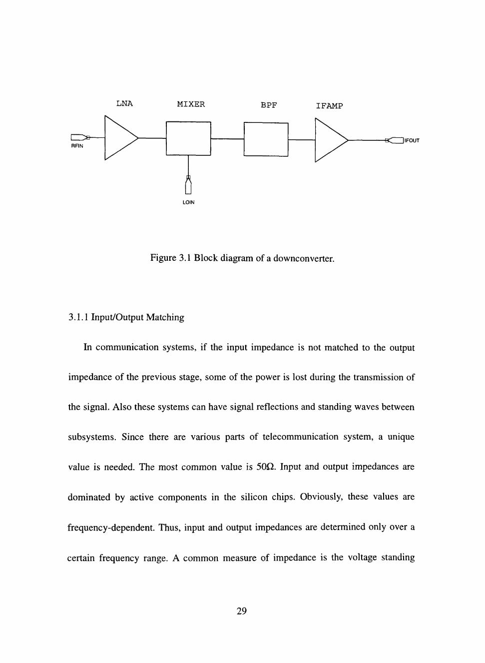
LNA MIXER BPF IFAMP
€C llFOUT
LOIN
Figure 3.1 Block diagram of a downconverter.
3.1.1 Input/Output Matching
In communication systems, if the input impedance is not matched to the output
impedance of the previous stage, some of the power is lost during the transmission of
the signal. Also these systems can have signal reflections and standing waves between
subsystems. Since there are various parts of telecommunication system, a unique
value is needed. The most common value is 50^. Input and output impedances are
dominated by active components in the silicon chips. Obviously, these values are
frequency-dependent. Thus, input and output impedances are determined only over a
certain frequency range. A common measure of impedance is the voltage standing
29

wave ratio which is defined as:
T7r.TT7r. l"!" I ^L, I
VSWR = , (3-1) \-\RL\' ^ ^
where RL is the retum loss:
7 -SO (RL),, =20\og\j-^\, (3-2)
Z is the impedance of interest. It is obvious that in perfect matching, VSWR = 1.
3.1.2 Conversion Gain
Conversion gain is used in a system where two inputs have two different
frequencies, such as in mixer cells. The term conversion means that the output signal
is converted from two input signals. For example, if a RF signal has a frequency, CQ,^p.
and a local oscillator has a frequency, <5J , the output IF signal has 0),^^ - cOj^f,. The
power conversion gain is defined as:
G„ = ^^^^ (3-3) I max
Maximum power is delivered when the input and output matching is achieved. If the
input and output impedances are matched to the same values,
Q (KnuLy^^y (3-4)
V If input and output impedance are 5012, (G^ )jg = 201og(-^^^).
imts
30

3.1.3 Nonlinearity
If an output of a system can be expressed by a linear combination of individual
inputs, the system is linear. For example, if a system has two inputs, xl(t) and x2(t),
Xiit)-^ y,{t), x^(t)-^y2(t),
where the arrow denotes the operation of the system, then
ax^ (t) + bx^ (t) -^ ay^ (t) + by^ (t), (3-5)
for all the values of the constants of a and b.
A system is called "memoryless" if the output does not depend on the past value
of input. The output signal v , of a memoryless nonlinear system is related to the
input signal v. as follows:
^our = ^0 + K^in + ^2^1 + ^3^1 +••• (3-6)
where k^ is the gain, 2 ^^^ 3 ^^ second- and third-order distortion coefficients
respectively. For a system, v.„ (t) = V cos(cot),
^out =^1^ cos(fi^) + A;2^^cos^(6;r)-l-A;3y^cos^(fty)-l-... (3-7)
Using the trigonometric properties,
v^^,=i^ + h,V'+-) + ik,V + h,V'+-)cos(ox) +
31

(^2^' + -—-- + ••') cos(2ft;f) + ( - ^ + '••) cosi3cot) + ••• (3-8)
The second term on the right-hand side of Equation (3-8) is the fundamental
frequency and higher terms are the harmonic frequencies. The harmonic distortion for
the iih component is defined as:
™ , = ^ , (3-9)
where b^ is the output fundamental frequency component factor and b. is the ith
harmonic component factor. Total harmonic distortion is defined as:
Jbl+bl+bl+"-b.
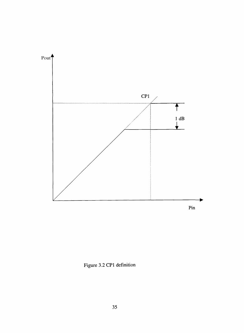
Due to these harmonic terms, as shown in Eq. (3-6), the output signal of a single
tone cannot be linear. Above a certain point, the output signal level deviates from its
ideally expected value by IdB. This is called IdB compression point (CPl). CPl is
defined with respected to either input or output of the system in cases where the
system gain is other than OdB. CPl can be calculated from
20logo 1 ^-k^yLB I) = 20log I k, I -\dB. (3-11)
Solving gives.
32

^ I - . B = J 0 . 1 4 5 | | L | . (3-12)
Figure 3-2 shows CPl.
For two-tone inputs which have the same power (magnitude),
Vm(0 = V cos{(ti,t) + V cosico^t), (3-13)
0) = 0)^,0)^ :{k^V +-/:3y')[cos(ty,f)-l-cos(6;20],
0) = (0^+0)2 : k2V^[cos((o^t + co^t) + cos{cOjt - Q)2t)],
3k V^ CO = 2(0^ ±0)2-. [cos(26;,r + C02t) + cos{2Q)^t - 0)2t)],
3k,V^ CO = 2ft?2 ± ^ 1 : [cos{2co2t + co^t) + cos(2ct)2t - 0)^t)].
Of all these frequencies, 2OJ^-OJ2 and 2^2 - ^i are the nearest frequencies to the
fundamental frequencies 6;, and 0)2. These frequencies may exist even after low
pass filtering. The fundamental frequency components increase proportional to V and
the third order terms are proportional to V^. If these were drawn in log scale, they are
straight lines. The third-order intercept point is defined to be at the intersection of the
two lines. Figure 3.3 shows the third-order intercept points, respectively. The
horizontal value of this graph is called input third-order intercept point (IIP3) and the
vertical value is called the output third-order intercept point (OIP3). Assuming that
V^ is much smaller than V, the input IP3 point is determined by
33

_ 3/ 3 ,,3 ..^^ 14. / : . ky=-^V'=>IIP3^J~\-^\. (3-14)
IIP3 in a cascade system is described as:
/ i i J\^ / I T
+ Td:;r+T7;;iT+'-- (3-15) IIP31 I1P3] IIP31 nP3]
where IIP3. are the third-order intercept point for each block and A. is the power
gain for corresponding block. Since the power gain is greater than unity, later blocks
are increasingly more critical. For example, IIP3 in the third stage is dominant of the
intermediate amplifier. Thus, we can focus only on the last stage only.
3.1.4 Noise
In telecommunication systems, noise generated in integrated circuits is very
important because this noise sets a lower bound on the signal level before problems
are encountered. Noise sources remained mysterious until Schottky, Nyquist and
Johnson published a series of papers that explained the origin and the amount of noise
sources. Johnson [25] reported careful measurements of noise in resistors for the first
time and his colleague Nyquist [26] explained them as a consequence of Brownian
motion. If the charge carriers are thermally agitated in a conductor, a randomly
varying current gives rise to a random voltage. Since this noise process is random, the
34
Pout'
CPl
'
t IdB
i
•
Pin
Figure 3.2 CPl definition
35

Pout
OIP3
OIP2
Fundamental
:.. IIP3
IIP2
3*'%rderi
IIP2 IIP3 Pin
Figure 3.3 IPn definition
36

value of voltage at a specific time cannot be identified. Thus the only resource to
characterize the noise source is statistical measures such as mean square values. Since
this noise originates from thermal agitation, it depends on temperature. The available
noise power is given by
P^^=kTAf, (3-16)
where k is the Boltzmann's constant and A/ is the noise bandwidth. Since the available
noise power is the same for all frequencies for the same bandwidth, this is often called
white noise.
For a single resistor, the power delivered by a noisy resistor to another resistor of
equal value is by definition
/ ' „ , = i r A / = ^ , (3-17)
where el is the open-circuit rms noise voltage generated by the resistor over the
bandwidth A/ at a given temperature. Therefore, the mean square open-circuit noise
voltage is
7„=4kTRAf. (3-18)
The noise current source which is corresponding to this mean square open-circuit noise
voltage is
37
.„ . ^ =4kTGAf. (3-19) 77 _ e: ^ 4kTAf
R^ R
A. Van der Ziel [27] derived an equation of noise for a MOSFET, which is
ll = 4kTyg,,Af , (3-20)
where g^^ is the drain-source conductance at zero V^^, and y is unity at zero V ,
and 2/3 for long channel devices. Van der Ziel [28] also has given the noise current for
gate in a MOSFET. Although this is negligible at low frequencies, it can be dominant at
radio frequencies.
il^ = 4kTSg Af, (3-21)
CO C ^ where the parameter g is —. Van der Ziel gives 4/3 (twice of y).
5g,o
Schottky [29] explained another noise mechanism in 1918. It is shot noise, also
occasionally call Schottky noise. For direct current flow and a potential barrier, charge
carriers hop over the barrier and generate discontinuous pulses, which cause shot noise.
The rms noise current is
il = 2qI^,Af, (3-22)
38

where q is the electron charge and /^^ is the DC current in Amperes. Note that, like
thermal noise, shot noise is white noise.
Another noise mechanism is flicker noise, which is known as 1//noise. Since this
has frequency dependence, this is also called "pink" noise compared to "white noise"
which is independent of frequency. This is the most mysterious type of noise. Yet it is
clear that some phenomena such as cell membrane potentials, the earth's rotation rate,
galactic radiation noise, and transistor noise have a l/f noise characteristic. Since this
characteristic is not verified clearly, all parameters for the equation are empirical.
Flicker noises in a resistor is
-^^K^_Ro_,y2^j: (3-23)
" / A
where A is the area of the resistor, K^ is the material specific parameter, which is
5x10"^^ 5^ -m^ for ion implanted resistors, 7? is the sheet resistance, and V is the
voltage across the resistor. The noise current for a MOSFET is
77 ^M 5 2
l_ = / "^LCl
A/ (3-24)
where g^ is the transconductance of the MOSFET, K^^ is also the material specific
parameter, which is about 5x10"^^ for PMOS and 50 time larger for NMOS, W and L
are the width and length of the MOSFET, and C„ is the thickness of gate oxide. The
39

noise current for a forward-bias junction is
'=yX' ' (3-25)
where the constant K. is around 5xlO~^^A-m^ A- is the area of the junction, and
/ is the current through the junction.
Finally, popcorn noise, also known as burst noise, has been exhibited in gold-
doped bipolar transistors. This noise was observed in point-contact diodes, but has also
been seen in ordinary junction and tunnel diodes, and all types of resistors. This noise
comes from contamination during the fabrication process but it is understood even more
poorly that 1//noise. The equation for this is
'N^ = ^ 4 / " . (3-26) l + (—)'
fc
Here K is a device and fabrication dependent empirical constant and /^ is a comer
frequency below which the burst noise density flattens out.
3.1.5 Noise Factor
The most commonly used quantity to measure noise characteristics in RF systems
is the noise factor, F which is given by:
40

s Signal - to - noise ratio at the input (—!-)
N P = ^ (3-27)
Signal - to - noise ratio at the output (— )
The noise factor expressed in dB is defined as the noise figure -NF. A
telecommunication receiver consists of different subsystems connected in cascade. For
cascade stages, the overall noise figure can be obtained in terms of the NF and gain of
each stage. The total noise factor is given by [30]
^ F , - 1 F3 - I F 4 - 1 ^ror=F,+--^ + - ^ + ---—r + -- (3-28)
where F. are the noise factors of the various blocks and G, are the corresponding
power gains. It is clear that the noise factor of the first block is dominant. The first
block in the RF receiver is a low noise amp. This block must have the lowest noise
possible and highest gain as well.
3.1.6 Low Noise Amp
As discussed in the previous section, a low noise amp (LNA) is the most crucial
part of a communication receiver because of its location. The noise factor and voltage
standing wave ratio (VSWR) are dominated by the LNA. Thus the LNA must have low
noise characteristics, high gain, good linearity, and low VSWR. Recendy a LNA which
has optimal noise figure of 0.95 dB, gain around 11 dB, 2mW of power consumption
41

has been manufactured using SiGe technology. Similar performance has been found in
GaAs designs [31]. On the contrary, CMOS implementations exhibit inferior
performance. For example, the NF is usually over 2.0 dB and power consumption is
around lOmW for CMOS circuits. But this technology has some advantages compared
to previous technologies. Because of its size, extremely low-cost CMOS designs are
very attractive. Another advantage is that most baseband designs in RF systems are
utilized by CMOS technology. Thus MOS design is the only one to lead to a one chip
receiver solution in the future. Furthermore, a new technology 4.5 mW 900 MHz
CMOS receiver for wireless paging has been realized [24]. This can provide more
impetus for low power CMOS receivers.
In addition to gain and noise figure, LNA's should have input and output
impedance matching and small signal linearity, which is described by the third order
intercept point. Thus LNA specifications will be determined by gain, noise figure and
third-order intercept point.
Figure 3.4 shows a simple CMOS LNA [21]. This can be considered as two stages,
an input stage and an output stage. As shown in Figure 3.5, NMOS transistors Ml and
M2, inductors LI and L2, and input resistor Rl comprise the input stage. In order to
find out the input impedance, equivalent circuits are drawn as in Figure 3.6. The input
42
impedance from Figure 3.6 is
where C ^ and gm are the gate-source capacitance and transconductance of Ml. At the
resonance frequency COQ = —======, the input impedance should be matched to
C,.
The matching method can achieve excellent noise figure because the signal is
amplified by Q (The signal is amplified by the Q of the mned circuit, it is a filter. The Q
indicates the sharpness of the filter and can reduce the noise not in the bandwidth of the
filter) before it reaches the noisy device. Q can be calculated by
e=,„V^=.„£.d^=_L^. (3-30) "" ° /? gmL^ co^gmL^
The dominant noise source in the LNA is the thermal noise come from the first
transistor (Ml). The channel noise is white with the power spectral density given by
% = 4kTn,, (3-31)
where k is the Boltzmann constant, g^^ is the zero-bias drain conductance of the
43

a.svAdr
300u
Figure 3.4 Schematic diagram of a low noise amplifier.
44

Figure 3.5 Input stage of LNA.
Figure 3.6 Input equivalent circuit of LNA.
45
device, and 7 is a bias dependent factor. For simplicity the condition gm = gj^ will
be used in this thesis. The body effect } is about 2/3 for long channel devices.
However, this value can be much higher than 2/3 for short channel devices [32, 33]. For
0.5 jum channel lengths, } may be as high as 2-3, depending on bias conditions [33].
The output noise power density due to the source R^
•2 2
'-^ = - ^ • Gm^ = 4kTR^ • Gm" (3- 32) A/ A/
where Gm is the effective transconductance due to Q, which is defined as:
Gm = gm • Q = . (3-33)
Thus
A/ to'.L] colL, ^ = 4 * ™ , - ^ ; r = - - j - f - (3-34)
The noise factor is
4kTR^ — -T 4kTygm + —^-^ „ -
F = i L ^ = g^^l+^^^o^-=l+ ^ =1 + ^ ^ . (3-35) i2 4kTR^ R^ Q'gmR, QR,
colL]
The noise figure which corresponds to this noise factor is
NF = 101og(l + —r^ ) = 101og(l + ^ ^ ^ ) . (3-36) Q'gmR/ QR,
46

This result shows several important features of this LNA architecture. First, the noise
figure is Q dependent. By choosing g > 1, the noise figure can be reduced significantly.
Second, the noise figure depends on gm.
Figure 3.7 and Figure 3.8 show the output stage and its equivalent circuit for AC
characteristics. Basically, the gain of the output amp is very high, the total gain is
Gm/?2. However, the transconductance of M3 is limited by the output current. Hence,
the LNA gain must be designed on the basis of a more accurate design equation. From
Figure 3.8, the gain of the output stage is
_R,,{\-gmR2) ^output ~ p , p ' ^^ ^ ' '
^2 + ^ O L
where /?(,/. i ^^^ parallel resistance of rds^^, /?2, and 7? . The output resistance is
^o.=L^'^f'^';' ,)N^3'l^.3. (3-38) l + gm,(R^+Zj,2)
where Z ,2 = O.2 (1 + ' i^rf.i) • (3-39)
3.1.7 Mixer
Down conversion mixers perform frequency translation by multiplying the two
signals from the RF amp and the local oscillator. The output signal, which is called the
intermediate frequency (IF) signal has a conversion gain and the frequency of the IF
signal is the frequency difference between RF frequency and LO frequency. The
47

vcc o-
IN
o-
, . R2 —vw
R3 <
M3 h ^
V.
Figure 3.7 Schemafic of LNA output stage.
Figure 3.8 Equivalent circuit for Figure 3.7.
48

important requirements of an RF mixer are input and output impedance matching, low
noise figure, high IP3 and moderate gain. Since the signal is amplified by the LNA, the
mixer must have sufficiendy low noise figure. Furthermore, neighboring base stations
often generate strong interfering signals in channels adjacent to the receiving channel.
Since these interfering signals cannot be filtered completely by the RF amp and other
filters, the small signal linearity, IP3, of the mixer should be sufficiently high to prevent
intermodulation.
In order to satisfy these conditions, usually single or double balanced mixers
(SBM's and DBM's, respectively) based on the Gilbert cell are used. The advantage of
using double balanced mixers is that they have higher conversion gain than that of
2 single balanced mixers. As will be seen later, the conversion gain for DBM's is — gm
n gm
while the conversion gain for SBM's is -^—. Another drawback of SBM's is LO-IF 71
feedthrough. As seen in Figure 3.9 [20] for a double balanced mixer, differential pairs
M7-M8 and M6-M9 add the amplified LO signal with opposite phase. This provides the
first-order cancellation. However, in SBM's, if the IF frequency is not much lower than
LO frequency, then a first-order low-pass filter following the mixer may not suppress
the LO feedthrough without attenuating the IF signal.
49

The conversion gain of the mixer shown in Figure 3.9 is
I IF =gmVi^oyRF^ (3-40)
where gm is the transconductance of M4 [34]. If V^^, =^mOj^,t and V^ =5^fi;^r,
4 1 I,P =gmsmco,^ptsqc0i^f^t = gm^mc0i^pt-{smo}j^ot+-s\n3o}i^fjt+--) (3-41)
n 3
Hence
2j?m J IF = cos(ftJ/f - fi?^ )f. (3-42)
n
The noise sources are divided into four parts: thermal noise from the load
transistors (Ml2 and Ml3), noise from the spectral density transistor load (MIO and
Mil) , noise from switching transistors (M6, M7, M8, and M9), and the RF input
transistors (M4 and M5).
Assuming that the thermal noise of the transistors dominate and noise due to
switching transistors and spectral density transistor loads are negligible compared to the
noise due to the RF input transistors and the load transistors. Then the noise referred to
the mixer input is
vl = 4kTr[— + U^f^]. (3-43) gm^ 2 2 gm^
Thus, the noise factor, if only the RF inputs transistors, are used depends on the ratio of
the transistor sizes.
50

vi •::= 3.3V . T
0
OUT-
M10
Figure 3.9 Schematic diagram of a mixer
51

3.1.8 Intermediate Frequency (IF) Amp
The output of the mixer is directly connected to the input of the intermediate
frequency (IF) amplifier. The IF amplifiers must have fairly high input impedance to
minimize the signal currents flowing in the mixer switches. The second condition for
the IF amplifier is the output impedance. The output impedance of the IF amplifier
should be well defined for use as a termination resistor for the filter that follows. The
third and one of the most important requirements of the IF amplifiers is high linearity.
The operating frequencies are moderate, so it is possible to use negative feedback to
linearize the amplifier. Negative feedback has the advantage that it does not require
close matching or tuning to perform well.
Figure 3.10 shows an IF amplifier and the complete topology for this amp. is
shown Figure 3.11. Since the last stage of the amplifier dominates the IP3
characteristics, the output stage needs to be as linear as possible. Several techniques are
used for this purpose. First, a push-pull class-A operation with a bias is used for the
output stage. Second, a suitable compensation technique is used to achieve the highest
linearity. Third, the nested Miller technique is the best choice for this because it
provides the maximum feedback around the output stage.
52

The noise performance is determined by the first stage. For noise considerations,
the input stage should be a fully differential pair without any differential feedback.
Since the amplifier is fully differential, a common-mode feedback is needed. The noise
referred to the IF amplifier is
v; = 4kTy[ + - ( - ) ' ^ ] . (3-44) gm, 2 2 gm.
The purpose of the middle stage is to provide gain, which is used to increase the
feedback around the output stage. This makes the IF amplifier more linear. The gain of
the input and middle stage is calculated as follows:
\i„ = ^ ^ . (3- 45) 1 -I- sr2 (C j -I- C3)
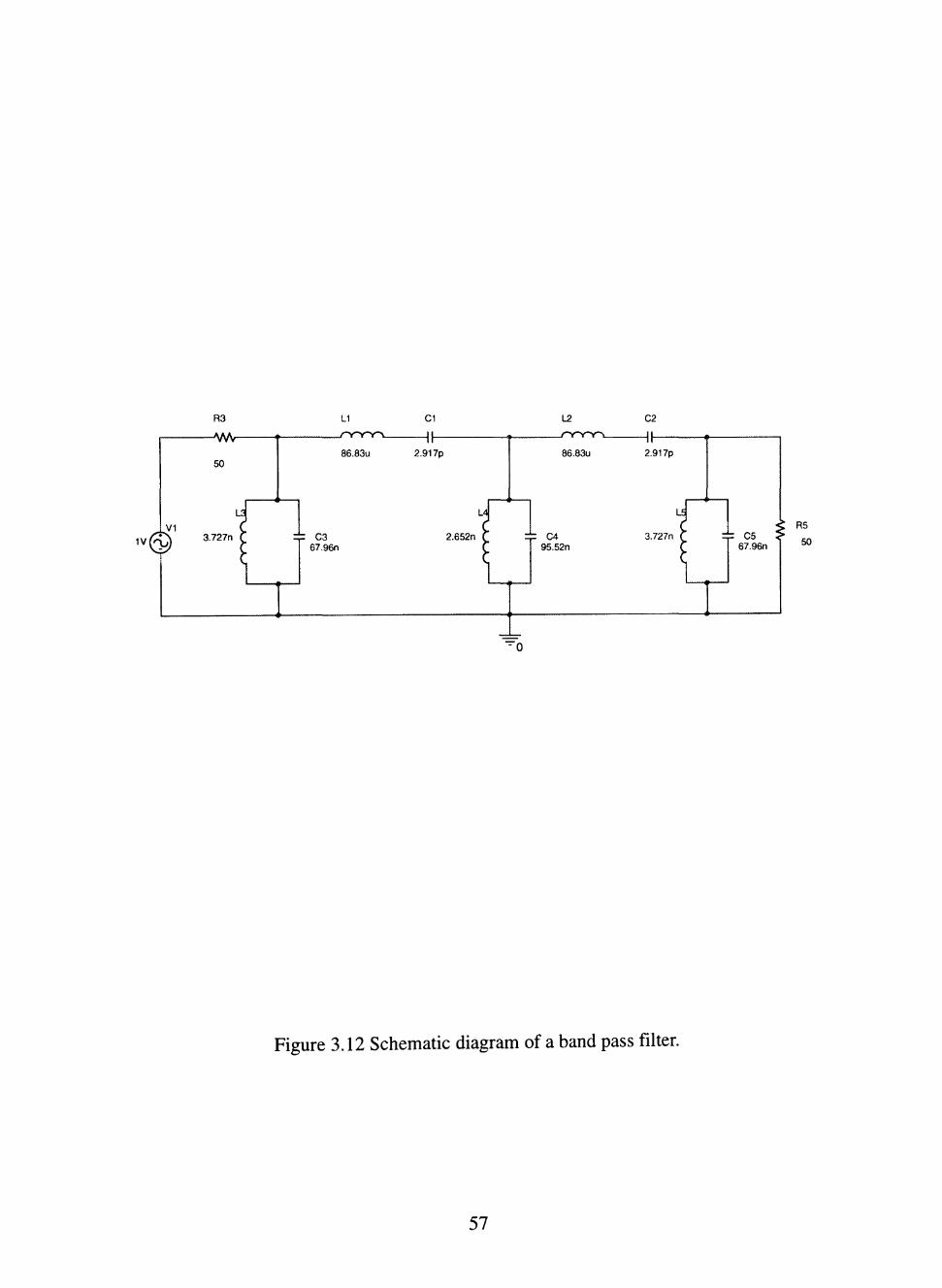
3.1.9 Band Pass Filter
Although an active filter can be implemented in the integrated circuit, it is the most
difficult to realize because the realization of high-Q filters is complicated by the lack of
suitable integrated inductors. Thus a passive filter is chosen. Figure 3.11 shows the
passive band pass filter.
In order to design a band pass filter for 80 MHz 5 -order Chebyshev low-pass
filter, which has 1 dB ripple, is chosen. Then this low-pass filter is converted to a band-
53

I:
400u
£ H
C140Ot
II 1
• ^
MI3
fit-H5 8k
M15
H3 M3 J 2.3V-±-
M 4 1 * ' - ^ 1000U
!i ch
( J ) ' " ^
M l
SOOu LphH* 13
M I O
1J3740U
alF -r
h-^-la ' M8 M B ' M
lOOu SOOu j
M11 12
1mA( - > 1 1r @
M ' 9 M20 -p
H5 H5
iJ Ep H5 ah
• — r
ce
HI f-
V2 - ± -
2.3V .-r
IA28 M29
M 2 3 M 2 1 I M
4ouffr
M 3 6
lOu
400UA©
5H
^a U32 20u
1 2u
H5
M 3 7 (
lOOu [
jHcir "'el-- X V3
1.55V
F"T~^1' M35
Ou
M3e
265u
65u
^ H3
? 4,4k
-^ H 4
Figure 3.10 Schematic diagram of an IF amplifier.
54

,C2 ,C2
V0Ut1
Rf
.CI
.y\
/
Rc <
/
<
N
Rf
C1
mirlrtip I f I I VI V I I w
staqe
inni it I I i r vwtb
Staqe
K
CM feedback vin1vin2
\ \ /
; = — ( I
ntithiif
Staqe
vout2
<; Rc
Figure 3.11 Equivalent block diagram of IF AMP.
55

pass filter, which has 800 kHz of bandwidth and the frequency is converted to 80 MHz.
Finally this circuit is changed for input and output resistors.
56
R3
•A/W-
50
L1 CI
.yyy^y^ | |
86.83U 2.917p
V1
1V o ; 3.727n ^ C3
67.96n
12
86.83U
C2
2.652n ^ C4 95.52n
2.917p
3.727n 4: C5 67.96n
R5
50
Figure 3.12 Schematic diagram of a band pass filter.
57
CHAPTER IV
RERULTS
4.1 Now Noise Amplifier
For a desired 15 dB of gain and a 1.5 GHz operating frequency, a low noise
amplifier (LNA) is designed. The output resistance is set to 50 Q. thus
l5dB = GmxR^^Gm = ^ = 0.1125 and 50
Gm = gm,Q = —^ => 4 = ^- = —, = 0.94nH . COQL^ co^xGm 2;rxl.5xlO'x0.1125
In order to reduce the noise figure and current consumption, a Q = 3 is selected.
gm, = - ^ = 0.0375. Q
Also gate-source capacitance is calculated as:
v9 ^ g m A , 0.0375X0.94X10-^^
'' R. 50
Since
C =-WLC„+WL,C^^ and Lis 0.25//m, gs /y OX a ox *
£ X£c^ r.^. 3.9x8.85x10"'^ C ^WLC =Wx0.25x-^ ^ = Wx0.25x .
'' "' t^^ 5.8x10"'
Thus the width of Ml transistor is 476 |im. Since the output impedance is matched to
50Q and from Chapter in,
^ R2+R,\\Z,,2 ^11^ II _ V ! j g i - | | / ? 3 ^ 5 0 a . ''"' \ + gm,{R,+Z,J l + gmA
58

_ RJR,+R2)-50{R, +R2+R.) Thus gm,=-^—^ \rM>n ' ^y choosing R, = 400Q, R2 = 120Q ,
50/v,/v,
and /?3=255a, gm, becomes 0.0184.
The locations of the poles are calculated as follows: since
^ r = ^ = - ^ ^ . 5 3 . 1 9 x l O V . J / . , Cgs 0.105 pF
f,,B=—^^ = \.5lGHz. gam X 271
From the previous chapter.
Cgs sCgs Zin =^^r^ + s{L^+^) + -^^. (4-1)
From this equation, the operating frequency co^ and the inductance L^ are obtained.
Since the operating frequency is set to 1.5 GHz, COQ should be the resonance
frequency of the input impedance. Thus,
CO, = - = = = = (4-1) ^Cgsm+L^).
Since Cgs = 0.705 pF, and L^ =0.94nF, L^ =14nF. Therefore two inductors L^
and L^, and a gate source capacitor has a tuned input circuit. The quality factor for
this circuit is set to 3. Hence, the transfer function is:
l + ^-S + —rs'' CO, CO,
59

This can be implemented to a Verilog-A code by using Laplace transform.
V(out) <+ laplace_nd(V(in), [1.0], [1.0, 2.0e-9, 4.44e-19];
The results for this implementation together with the real circuit simulation results are
shown in Figure 4.1. Both have around 14 dB gain and two poles around 1.5 GHz.
The schematic simulation result has a lower bump because the real circuit has lower Q
values than Verilog-A code due to the parasitic capacitors and resistors.
Both thermal noise and flicker noise contribute to the output noise. Even though
the flicker noise contribution is very low at high frequency (near IGHz), it is also
interesting to see the —characteristics at low frequencies. This flicker noise also
depends on the transistor sizes,
in_^ Kf L^KcolA. (4-3) A/ WLCox f f
60

c^: Verilog 20 ' : Schematic
10
0.0
m - 1 0
- 2 0
- 3 0
- 4 0 IK laK
dconv Inclesl. schemcUc : OverlciO Results
AC RsspansB
• • • • ' "
100K 1M 10M freq ( H2 )
100M 1G 10G
Figure 4.1 AC Response for Schematic and VerilogA Results in LNA
61

The Verilog-A code for this noise is shown below.
I{LNAOUT) <+ Gm*vod/2;
V(LNAOUT) < + I(LNAOUT)* Rout;
I(LNAOUT) <+ flicker_noise(kf*pow(abs(I(LNAOUT)),af) ,ef);
I(LNAOUT) <+flicker_noise(argl*Gm*pow(abs(I(LNAOUT)),
0 . 0) , 0 . 0 ) ;
The noise simulation results are shown Figure 4.2. The flicker noise contribution
is very small even at 1 kHz. The thermal noise difference between two results is about
3 nV I-JHZ, which is small. The VerilogA code for all simulations is shown in Figure
4.3.
In order to obtain theoretical IIP3 value, I-V relationship is described as [35]
W [y,{t)-V^^,-Vtf _\ + 2pV^{t) + P'V^{ty-
/zxo - "^^^z . l + ( V / 0 - V , . o - ^ 0 l + « V / 0 ' (4-4)
62

where a- and p-i+^(v^..o-^o y,s.-yt
A Collecting the third-order terms and the first-order terms for the magnitude of —;=,
V2 A 3a{B-af , A , . 3(%„ A ,
gives — = = ^ —(—=)-=—^p^(—)\
2V2 4 2/3-a 2V2 32V27 2
Thus IIP3 in dBm is
IIP3 = 10[1 -h l o g ( i ^ ) - log(^) - l o g ( ^ ) ] , (4-5)
where 6 is known to be 0.1-10 for MOS transistors. Thus IIP3 can be calculated for
the low noise amplifier. This value is approximately 10.826 dBm. SpectreS uses
power as a sweep variable to simulate this value. Unfortunately, however, Verilog-A
does not have any variable to handle a power quantity.
4.2 Mixer
2 The conversion gain of the mixer is — gmR^. For a standalone mixer, the output
71
resistance is 20 kQ. Thus gmR^^ ~ 1. This makes the conversion gain for a standalone
circuit equal to -3.9 dB. Figure 4.4 shows the conversion gain for the schematic and
the Verilog-A. The RF input has 920 MHz and the local oscillator (LO) has 1 GHz so
that the output intermediate frequency (IF) becomes 80 MHZ. Until 80 MHz, the
conversion gain is almost constant.
63

Noise for LNA
Singls Pofnt Periodic Staady Siate Reaponae
4.0n "•
Schematic Verilog
3.0n
X 2.0n .
1.Sn
0.0 • > • * • I
10K 100K IM freq { Hs )
10M 100M 1G
Figure 4.2 Noise Currents in LNA
64

// VerilogA for "dconv", "Inaverilog", "veriloga"
'include "constants.h"
'include "discipline.h"
module Inaverilog(LNAIN, LNAOUT);
input LNAIN;
output LNAOUT;
electrical LNAIN, LNAOUT;
real Rout, Rs, Rl, R2, R3, Gm, Cgs, Ls, Lg, gml, gm3;
real vod, kf, af, ef, argl, w, 1;
analog begin
w = 47 6;
1 = 0.25;
af = 1.0;
ef = 1.0;
kf = 1.0e-12*5.8e-9/(w*l*1.0e-12*3.9*8.85e-12);
kf = 2.44e-15 // kf = kf'wt^2WL
gain =5.62; // gain = 15 dB
vod = 0.04;
argl = 3.3e-20; // arg2 = 4kT*gamma
fO = 1.5e9;
Rout = 50;
Gm = gain/Rout; // Gm = 0.1125
V(LNAOUT) <+ gain * laplace_nd(V(LNAIN)/2, [1.0],
[1.0, 2.205e-10, 4 . 3757e-20]);
I(LNAOUT) <+ Gm*vod/2;
V(LNAOUT) < + I(LNAOUT)* Rout;
I(LNAOUT) <+ flicker_noise(kf*pow(abs(I(LNAOUT)),af) ,ef) ;
I(LNAOUT) <+ flicker_noise(argl*Gm*
pow(abs(I(LNAOUT)),0.0),0.0);
end
endmodule
Figure 4.3 VerilogA Code for LNA Simulation
65
The thermal noise of the mixer, as calculated in the previous chapter, is
1 TT 2 8^7 [1+ —(—) -] times the thermal noise of the single input transistor. Since
2 2 gm^ sm I— — - ~ V2 , the total thermal noise of the mixer is 1.8 times larger that the noise for a
single transistor. These results together with flicker noise are shown Figure 4.5.
The linearity in the mixer is very important for a down conversion mixer for
several reasons. First, unwanted signals from other channels in the receiver are
amplified through the LNA and reach the mixer without filtering. Second, the linearity
of the second block in the cascade system contributes to the linearity more than the
first block. The real calculation of the linearity of the mixer is identical to that of the
LNA. From the previous section,
IIP3 = 10[1 + l o g ( i 2 ^ ) - log(6>) - l o g ( ^ ) ] . (4.6)
For 0.6V of bias, IIP3 = 10.8 dB. Once again, Verilog-A does not have a power
variable. The calculation results shown above and the simulation results for the
schematic are shown in Figure 4.6. This results show that IIP3 for the mixer is 4.58,
which is lower than the theoretical calculation. This is because the load devices (both
resistors and PMOS devices) are not included in the calculation. Also the VerilogA
code for mixer simulation is shown in Figure 4.7.
66

Conversion <,'c:i.'i for Mixer
Sfngls Pofnt Periodic Steady S^ate Reaponae
c: VerilogA 3 v. Schematic
> m
-1
- 2
- 3
- 5 IM
'
•freq < Hz ) 100M
Figure 4.4 Conversion Gain for Schematic and VerilogA in Mixer
67

Noise for Mixer
Sfngle Point Periodic Steady State ReaponaE
-: schematic 140n '• Verilog
100K 1U freq < Hz )
10M >•«£
liai^M 1G
Figure 4.5 Noise Currents in Mixer
68

-10.0
-20.0
-30.0
-40.0
-50.0
S -60.0
-70.0
-S0.0
-90.0
-100
-110
•
-
-
-
-
-
-
L.
Ida^dG? 3dBy'dB
' • 1 r 1
[[P3 -for miKsr
Swept Periodic Steady State Response
^ : lat order n: 3rd order
- 3 0
IP3 point .^ 4.56756
• • • ' ' ' I I I I I ' • • I I I I I • • • I I L J I I I I i _ _i I i__i I I i_J
- 2 0 - 1 2 prf
0.0 W Z0
Figure 4.6 Input Third-Order Intercept Point for Schematic in Mixer
69
4.3 IFAMP
The IF AMP has three poles. Each comes from the input stage, middle stage, and
output stage. The third pole is compensated by a capacitor. So the locadon of the third
pole is very high compared to the first two poles. Voltage gains and poles are
calculated similar for the first two stages. Total DC gain is
Av = gm,gm2R„,R„2^ (4-8)
where R^^ and R^2 ^^ ^^^ parallel combination of PMOS and NMOS transistors.
The calculation of the DC gain is 45.5 dB.
Since the bias current and transistor sizes are different between the first stage and
the second stage, locations of the poles are diff'erent. These are calculated as:
1 w, = ,
where Cj = C ^ + C ^ + C^j . The first pole is located at 335 MHz. Similarly, the
location of the second pole is 906 MHz.
The AC response of the IFAMP is simulated and compared to the VerilogA
simulation results in Figure 4.8. The gain for the VerilogA simulation is lower than
that for the schematic simulation. This is because VerilogA code does not include the
buffer output stage. The two different poles are seen clearly in the schematic results
because of the compensation by a capacitor.
70

IFAMP has too much noise compared to mixer and LNA. This noise is calculated
by the first stages. Compared to the noise calculation in the mixer, which comes from
the NMOS and PMOS combination. The bias current is too large and the transistor
sizes are relatively large compared to those in the mixer and LNA. This causes the
larger noise contribution. These results are shown in Figure 4.9 and the VerilogA code
is shown is Figure 4.10.
4.4 Band Pass Filter
From Figure 3.12, the transfer function of the band pass filter can be calculated
as below.
H{s) = H,{s)H2(s)H,is), (4-6)
where
9.318x10'''.y ^'^^^ l-H9.318xl0-''5 + 3.9575xl0-''5' '
H2(s) = 1.2078xl0"''5'
' ^ ^ " 1 + 3.9578x10-^^5'+1.5651x10-^^/'
1.699x10-''^' 1-h 3.9578x10"''5'+1.5663x10"''5'
71

// VerilogA for "dconv", "mixerverilog", "veriloga"
'include "constants.h"
'include "discipline.h"
module mixerverilog (RFINP, RFINM, LOINP, LOINM, MIXOUTP, MIXOUTM);
output MIXOUTP, MIXOUTM;
input RFINP, RFINM, LOINP, LOINM;
electrical RFINP, RFINM, LOINP, LOINM, MIXOUTP, MIXOUTM;
parameter real gain=2.0/'M_PI;
real gm, kf, argl, arg2;
real vod, af, ef, uCox, w, vth;
analog begin
w = 80;
vth = 0.56;
kf = 1.0e-22*5.8e-9/(w*1.0e-12*3.9*8.85e-12) ;
// kf = kf'/(WLCox)
af = 1.0;
ef = 1.0;
vod = 0.04;
uCox = 108e-6;
argl = 3.3e-20; // arg2 = 4kT*gamma
gm = 1.12e-3;
V(MIXOUTP) <+ gain*V(RFINP,RFINM)*V(LOINP, LOINM) ;
I(MIXOUTP,MIXOUTM) <+ 1.0e-6*uCox*w*(V(RFINP,RFINM)-vth)
*(V(RFINP,RFINM)-vth)/(1+V(RFINP,RFINM)-vth);
I(MIXOUTP,MIXOUTM) <+ gm*vod/2;
I(MIXOUTP,MIXOUTM) <+ flicker_noise(kf*
pow(abs(I(MIXOUTP,MIXOUTM)),af),ef);
I(MIXOUTP,MIXOUTM) <+ flicker_noise(argl*gm*
pow(abs(I(MIXOUTP,MIXOUTM)),0.0).0.0);
end
endmodule
Figure 4.7 VerilogA code for Mixer Simulation
72

- : VerilogA QQ I : Schematic
> m
50
40
30
20
10
0.0
- 1 0
- 2 0
AC Response for IFAMP
AC RespansB
IK .i-ml. I I I I I ' • • • " • • — • ' ' • • 1 ^ • • • • ' • • " • • ' — I i X . l l
laK 100K IM 10W freq ( H2 )
100M IC i0c;
Figure 4.8 AC Response for Schematic and VerilogA Simulation in IFAMP
73

IM
cr u
Noiae for IFAMP
Smgle Pomt Periodic Steady Siate Reaponae
i : Schematic 1u - : VerilogA
10M freq ( H2 )
Figure 4.9 Noise Simulation for Schematic and Verilog in IFAMP
74
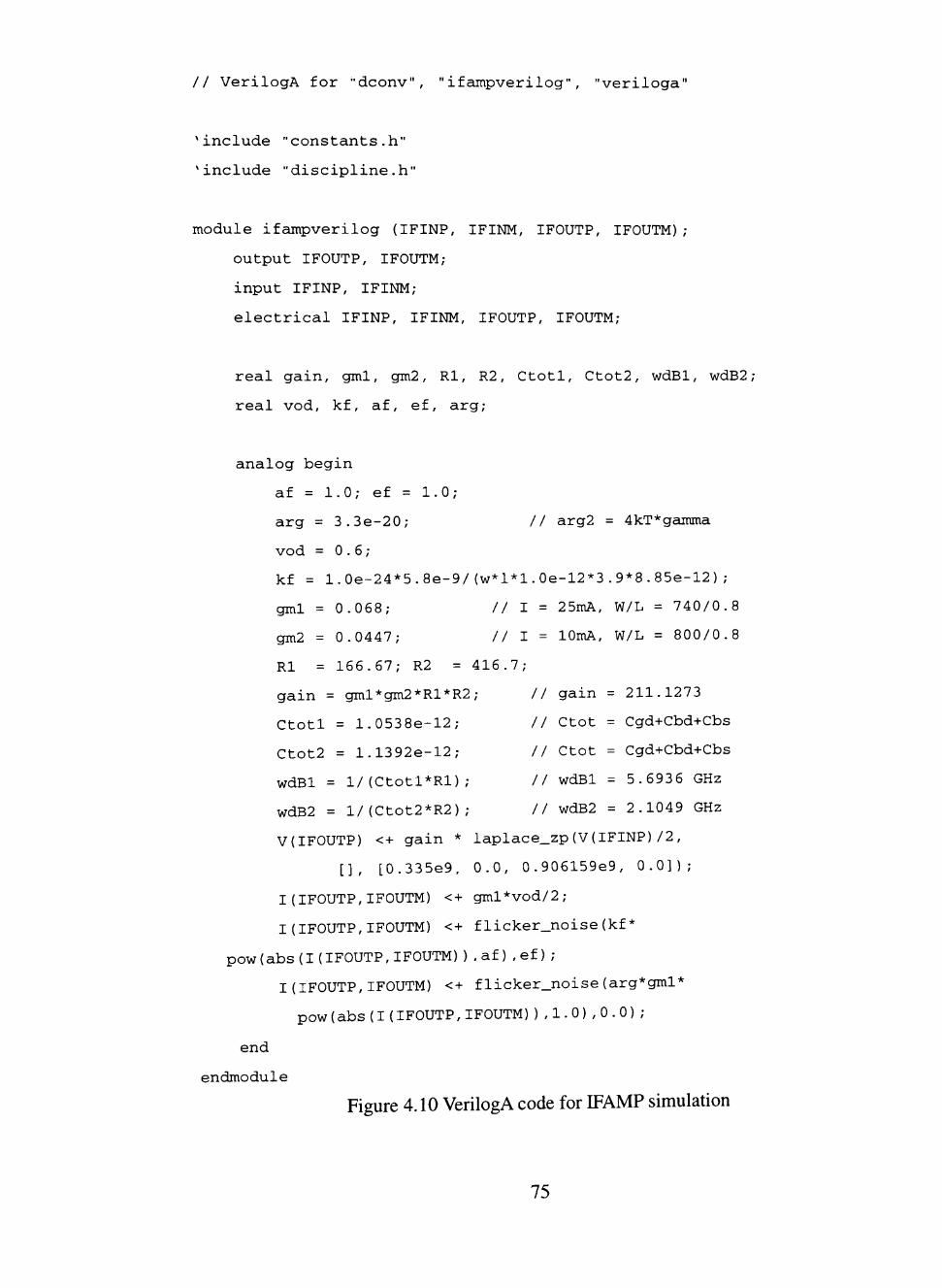
// VerilogA for "dconv", "ifampverilog", "veriloga"
'include "constants.h"
'include "discipline.h"
module ifampverilog (IFINP, IFINM, IFOUTP, IFOUTM);
output IFOUTP, IFOUTM;
input IFINP, IFINM;
electrical IFINP, IFINM, IFOUTP, IFOUTM;
real gain, gml, gm2, Rl, R2, Ctotl, Ctot2, wdBl, wdB2;
real vod, kf, af, ef, arg;
analog begin
af = 1.0; ef = 1.0;
arg = 3.3e-20; // arg2 = 4kT*gamma
vod = 0.6;
kf = 1.0e-24*5.8e-9/(w*l*1.0e-12*3.9*8.85e-12);
gml = 0.068; // I = 25mA, W/L = 740/0.8
gm2 = 0.0447; // I = 10mA, W/L = 800/0.8
Rl = 166.67; R2 = 416.7;
gain = gml*gm2*Rl*R2; // gain = 211.1273
Ctotl = 1.0538e-12; // Ctot = Cgd+Cbd+Cbs
Ctot2 = 1.1392e-12; // Ctot = Cgd+Cbd+Cbs
wdBl = 1/(Ctotl*Rl); // wdBl = 5.6936 GHz
wdB2 = l/(Ctot2*R2); // wdB2 = 2.1049 GHz
V(IFOUTP) <+ gain * laplace_zp(V(IFINP)/2 ,
[], [0.335e9, 0.0, 0.906159e9, 0.0]);
I(IFOUTP,IFOUTM) <+ gml*vod/2;
I(IFOUTP,IFOUTM) <+ flicker_noise(kf*
pow(abs(I(IFOUTP,IFOUTM)),af),ef);
I(IFOUTP,IFOUTM) <+ flicker_noise(arg*gml*
pow(abs(I(IFOUTP,IFOUTM)),1.0),0.0);
end
endmodule
Figure 4.10 VerilogA code for IFAMP simulation
75

These results are shown in Figure 4.11. The schematic resuh has very small ripple
because this is designed as a 5^ -order Chebyshev filter with IdB ripple. It is very hard
to limit the ripple in the VerilogA code. The VerilogA code for this simulation is
shown in Figure 4.12.
As a result, VerilogA and schematic simulations have almost the same DC gains
and locations of poles for LNA, miser, IF AMP, and BPF. Noise current in the mixer
is acceptable and comparable for both VerilogA and schematic simulations. However,
noise currents in the LNA and IFAMP are very high and are different for two results.
Even though IIP3 can not be simulated directly by VerilogA, VerilogA can be used to
modify and simulate circuits quickly especially for large systems.
76

100 - : Schematic I : Verilog
Q.m
m
-100
- 2 0 0 70M
Bond Pas5 Filter
AC RespansB
7BM B2M freq ( H2 )
90 M
Figure 4.11 AC Response for Schematic and VerilogA in Band Pass Filter
77

// VerilogA for "dconv", "bpfverilog", "veriloga"
'include "constants.h"
'include "discipline.h"
module bpfverilog (BPFOUT, BPFIN);
output BPFOUT;
input BPFIN;
electrical BPFOUT, BPFIN;
electrical VI, V2;
parameter real gain=1.0;
parameter rl=50; cl=8.4944e-9; c2=0.36466e-12; c3=11.94e-9;
parameter real c4 = c2; c5=cl; 11 = 0.4659e-9 ; 12 = 10.8533e-6;
parameter real 13=0.3312e-9; 14=12; 15=11;
parameter real a=ll/rl from(0:inf); b=cl*ll; c=c2*13;
parameter real d=c2*12+c3*13 + c2*13; e=c2*c3*12*13 ;
parameter real f=c4*15; g=c4*14+c5*15 + c4*15;
parameter real h=c4*c5*14*15;
analog begin
V(V1) <+ gain * laplace_nd(V(BPFIN),
[0.0, 9.318e-12], [1.0, 9.318e-12, 3 .9575e-18]);
V(V2) <+ laplace_nd(V(Vl), [0.0, 0.0, 1.2078e-22],
[1.0, 0.0, 3.9578e-18 + 3.9545e-18, 0.0, 1.5651e-35]);
V(BPFOUT) <+ laplace_nd(V(V2), [0.0, 0.0, 1.699e-22],
[1.0, 0.0, 3.9578e-18+3.9575e-18, 0.0, 1.5663e-35]);
end
endmodule
Figure 4.12 VerilogA Code for BPF Simulation
78

CHAPTER V
CONCLUSIONS
A VerilogA analog hardware description language (AHDL) is used to simulate
circuits in the radio frequency telecommunication system. In digital system, hardware
description languages generate circuits or netlists automatically and this makes
possible auto-layout. In analog systems, however, this is not done yet. For auto-design,
first, cell libraries using AHDL's should be generated and analog designers choose the
blocks to design a system easily. This procedure is iterated until the design meets the
specifications. Using real circuits, this takes much longer than using AHDL's because
real circuit design must think about the transistor level modifications such as transistor
sizes, schematic diagrams, and process parameters. Analog designers cannot get the
results easily by changing only one transistor size. They have to change whole circuit
blocks or, even worst cases, the whole circuits and also think about the process
parameters. AHDL codes, however, can get desired results by modifying one or two
lines. As a first step, in this thesis, VerilogA code blocks are written for a RF system
and simulated to compare the results by conventional simulations. If this is satisfied,
analog designers can choose VerilogA blocks, which match the specifications, to
design large systems without modifying the transistor level circuit one by one. Once
79

top-level designs are finished only with VerilogA codes, real circuit blocks are
designed to have the same characteristics as VerilogA blocks.
This system, which is used in this thesis is a down converter. This system has
four different circuit blocks. Four VerilogA code blocks for low noise amplifier (LNA),
mixer, intermediate amplifier (IF AMP), and band pass filter, are written and
simulated using SpectreRF simulator by Cadence and the results are compared to
circuit simulation results for the possibility of using VerilogA code blocks instead of
real circuit blocks like in digital systems.
DC gains and AC responses for each block are compared and matched pretty well.
For the band pass filter, those results are almost identical except the ripples. Since the
schematic circuit has been designed by 5*-order Chevy she v filter with IdB ripples,
ripples in the output are controlled less than 1 dB. For the rest of the blocks, DC gains
and the pole locations are similar. Noise characteristics are also simulated. Thermal
noise and flicker noise are included. Simulation results for the mixer are fairly
acceptable. However, results for the LNA and IF AMP have big difference. VerilogA
simulation results for LNA and IF AMP are similar to those for mixer. Thus real
circuits might not be well optimized to the process that we use. Another important
value to be checked in the telecommunication systems is the input third order intercept
80

point to verify the linearity of the systems. However, VerilogA code cannot handle this
simulation because the input and output parameters of this simulations are powers.
VerilogA does not have any power inputs and outputs. For this reason, simple
calculations and circuit simulation results are compared.
Even though VerilogA has lots of limitations for analog circuit simulations, basic
function blocks such as DC gains and AC responses working well for VerilogA
simulations. Thus, VerilogA code blocks can be used to design circuits especially for
large systems to see basic characteristics quickly without changing the circuits in
detail.
81

REFERENCES
1. T. L. Quarles, Analysis of Performance and Convergence Issues for Circuit
Simulation, Ph. D. thesis. University of California, Berkeley, 1989.
2. R. Saleh, S-J Jou and A. R. Newton, Mixed Mode Simulation and Analog Multi-
Level Simulation, Kluwer Academic Publishers, Boston, MA, 1994.
3. MHDL Language Reference Manual, Intermetrics, Inc., February 1995.
4. IEEE 1076.1 (VHDL-AMS) Design Objective Document, IEEE, 1999.
5. Verilog-AMS iMnguage Reference Manual, Open Verilog International, 1999.
6. H. A. Mantooth and M. Fiegenbaum, Modeling with an Analog Hardware
Description Language, Kluwer Academic Publishers, Boston, MA, 1995.
7. E. Liu, Analog Behavioral Simulation and Modeling, Ph. D. Dissertation,
University of California, Berkeley, 1993.
8. T. Quaries, SPICE3 Version 3c 1 User's Guide, Memorandum UCB/ERL M89/46,
UC Berkeley, 1989.
9.1. Getreu, A. Hadiwidjaja, and J. Brinch, "An Integrated-circuit comparator
Macromodel," IEEE Journal of Solid State Circuits, SC-11, 826, 1976.
10. G Boyle, B. Cohn, D. Pederson, and J. Solomon, "Macromodeling of integrated
circuit operational amplifiers," IEEE Journal of Solid State Circuits, SC-9, 353,
1974.
11. MicroSim Corporation, Circuit Analysis User's Guide Version 5.0, MicroSim
Corporation, July 1991.
12. Meta-Software, HSPICE User's Manual H9001, Meta-Software, 1990.
82
13. E. Tan, Phase-locked loop macromodels. Master's thesis, UC Berkeley, August
1990.
14. G. Casinovi and A. Sangiovanni-Vincentelli, "A macromodeling algorithm for
analog circuit," IEEE Trans, on CAD, 10, 150, 1991.
15.1. Getreu, Behavioral modeling of analog blocks using the SABER simulator, Proc.
MWCAS, 977, August 1989.
16. J. Singh and R. Saleh, "iMACSIM: A program for multi-level analog circuit
Simulation," Proc. IEEE ICCAD, 16, November 1991.
17. V. Ma, J. Singh, and R. Saleh, "Modeling, simulation, and optimization of analog
macromodels," CICC, May, 1992.
18. S. C. Fang, Y. P. Tsividis, and O. Wing, "SWITCAP: a switched capacitor network
analysis program." IEEE Circuits Syst. Mag, 5, 4, 1983.
19. L. A. Williams, B. E. Boser, E. W. Y. Liu, and B. A. Wooley, MIDAS user manual.
Center for Integrated Systems, Stanford University, 1989.
20. A. Rofougaran, J. Y. C. Chang, M. Rofougaran, and A. A. Abidi, "A 1 GHz
CMOS RF Front-End IC for a Direct-Conversion Wireless Receiver," IEEE J. of
Solid State Circuits, 31, 880, 1996.
21. Q. Huang, P. Orsatti, and F. Piazza, "GSM Tranceiver Front- End Circuits in
0.25|im CMOS," IEEE J. of Solid State Circuits, 34, 292, 1999.
22. A. R. Shahani, D. K. Shaeffer, and T. H. Lee, "A 12-mW Wide Dynamic Range
CMOS Front-End foe a Portable GPS Receiver," IEEE J. of Solid State Circuits, 32,
2061, 1997.
23. H. Samavati, H. R. Rategh, and T. H. Lee, "A 5-GHz CMOS Wireless LAN
Receiver Front End," IEEE J. of Solid State Circuits, 35, 765, 2000.
83

24. H. Darabi and A. A. Arabi, "A 4.5-mW 900-MHz CMOS Receiver for Wireless
Paging," IEEE J. of Solid State Circuits, 35, 1085, 2000.
25. J. B. Johnson, "Thermal Agitation of Electricity in Conductors," Phys Rev, 32, 97, 1928.
26. H. Nyquist, "Thermal Agitation of Electric Charge in Conductors," Phys Rev, 32, 110, 1928.
27. A. van der Ziel, "Thermal Noise in Field Effect Transistors." Proc. IEEE, 1801,
August 1962.
28. A. van der Ziel, Noise in Solid Circuit Devices and circuits, Wiley, New York,
1986.
29. W. Scottky, "On spontaneous Current Functions in Various Electrical Conductors,"
Annalen der Physik, 57, 1918.
30. U. L. Rohde and T. T. N. Bucher, Communication Receivers: Principles and
Design, McGraw Hill, New York, 1994.
31. L. E. Larson, "Integrated Circuit Technology Options fir RF IC's - Present Status
and Future Directions," IEEE 1997 CICC, paper no. 9.1.1, pp 169, 1997.
32. B. Wang, J. R. Heliums, and C. G. Sodini, "MOSFET thermal noise modeling for
analog integrated circuits," IEEE J. Solid State Circuits, 29, 833, 1994.
33. A. A. Abidi, "High-Frequency Noise measurement on FET's, with small
dimensions," IEEE Trans, on Elec. Devices, ED-33, 1081, 1986.
34. J. N. Babanezhad and G. C. Temes, "A 2-V Four-Quadrabt CMOS Analog
Multiplier," IEEE J. Solid State Circuits, 20, 1158, 1985.
35. Q, Huang, F. Piazza, P. Orsatti, and T. Ohguro, "The Impact of Scaling Down to
Deep Submicron on CMOS RF Circuit," IEEE J. Solid State Circuits, 33, 1023,
1998.
84

PERMISSION TO COPY
In presenting this thesis in partial fulfillment of the requirements for a master's
degree at Texas Tech University or Texas Tech University Health Sciences Center, I
agree that the Library and my major department shall make it fi-eely available for
research purposes. Permission to copy this thesis for scholarly purposes may be
granted by the Director of the Library or my major professor. It is understood that
any copying or publication of this thesis for financial gain shall not be allowed
w ithout my further vmtten permission and that any user may be liable for copyright
infringement.
Agree (Permission is granted.)
Student Signature Date
Disagree (Permission is not granted.)
Student Signature Date