analog integrated circuits lecture 3: single stage ... • ac analysis: – find ac equivalent...
TRANSCRIPT

Analog Integrated Circuits
Lecture 3: Single Stage Amplifiers
and Differential Amplifiers
Analog Integrated Circuits
Lecture 3: Single Stage Amplifiers
and Differential Amplifiers
ELC 601 – Fall 2013
Dr. Ahmed Nader
Dr. Mohamed M. Aboudina
Department of Electronics and Communications Engineering
Faculty of Engineering – Cairo University

10/27/2013
Contents
• Single-Stage Amplifiers
– Common source (with and without degeneration)
– Common drain
– Common gate
– Cascoding Concept
– Folded Cascode Amplifier
• Differential Pair
– Bipolar-based Differential Pair.
– MOSFET-based Differential Pair.
– Gilbert Cell
© Ahmed Nader, 2013
2

Single-Stage Amplifiers: General Concepts
10/27/2013
MOSFET is biased in saturation region by dc voltage source VGS. Q-point
is set at (ID, VDS) = (1.56 mA, 4.8 V) with VGS = 3.5 V.
Total gate-source voltage is: vGS=V
GS+v
gs
1 V p-p change in vGS gives 1.25 mA p-p change in iD and 4 V p-p change
in vDS.
© Ahmed Nader, 2013
3

Single-Stage Amplifiers: DC and AC Analysis
10/27/2013
• DC analysis:
– Find dc equivalent circuit by replacing all capacitors by open circuits
and inductors by short circuits.
– Find Q-point from dc equivalent circuit by using appropriate large-
signal transistor model.
• AC analysis:
– Find ac equivalent circuit by replacing all capacitors by short circuits,
inductors by open circuits, dc voltage sources by ground connections
and dc current sources by open circuits.
– Replace transistor by small-signal model
– Use small-signal ac equivalent to analyze ac characteristics of amplifier.
– Combine end results of dc and ac analysis to yield total voltages and
currents in the network.
© Ahmed Nader, 2013
4

Single-Stage Amplifiers: General Concepts
Amplifier
Amplifier Amplifier
10/27/2013
outmvRGA −=
© Ahmed Nader, 2013
5

Common-Source Amplifier
10/27/2013
What is the output voltage swing?
© Ahmed Nader, 2013
6

Common-Source Amplifier with Active Load
10/27/2013
Max or Intrinsic Gain
Gain is inversely proportional to current
What is the DC level at the output?
© Ahmed Nader, 2013
7

Common Source with Degeneration
10/27/2013 © Ahmed Nader, 2013
8

10/27/2013
Common-Drain Amplifier (Source Follower)
© Ahmed Nader, 2013
9

10/27/2013
Source Follower: What about body effect?
© Ahmed Nader, 2013
10

Common-Drain Amplifier (Source Follower)
Other source follower examples:
10/27/2013
Voltage shifting (headroom problems)
Non-linearity
© Ahmed Nader, 2013
11

Common-Gate Amplifier
10/27/2013 © Ahmed Nader, 2013
12

Common-Gate Amplifier
10/27/2013
Positive gain
Low input impedance
Large output impedance
© Ahmed Nader, 2013
13

Cascode Stage: Concept of Cascoding
10/27/2013 © Ahmed Nader, 2013
14
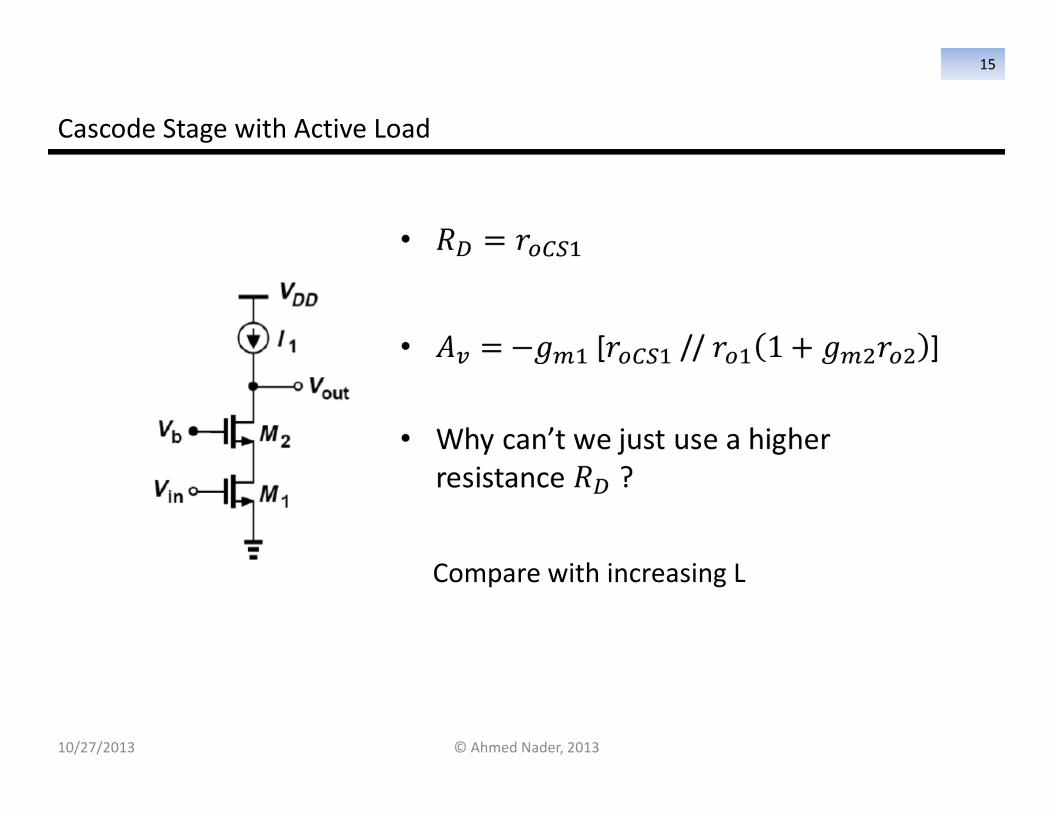
Cascode Stage with Active Load
10/27/2013
Compare with increasing L
© Ahmed Nader, 2013
15
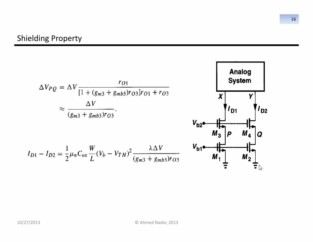
Shielding Property
10/27/2013 © Ahmed Nader, 2013
16

Triple Cascode
10/27/2013
Output impedance ~ ro (gmro)2
Not very friendly with low voltage applications
© Ahmed Nader, 2013
17

Cascode Current Source
10/27/2013 © Ahmed Nader, 2013
18

How can we increase the gain even more ?
10/27/2013
Gain Enhancement
Using Negative load resistance
Assignment 2b: Prove that Z1 is equal = -2/gm
© Ahmed Nader, 2013
19

Folded Cascode
• Input and Cascode devices need not be of the same type.
10/27/2013 © Ahmed Nader, 2013
20

Folded Cascode
10/27/2013 © Ahmed Nader, 2013
21

Assignment2c: Identify the type of each amplifier
10/27/2013 © Ahmed Nader, 2013
22

Differential Pair
Differential vs. Single-ended Operation
• A single-ended signal is measured with respect to a fixed
reference (usually GND).
• A differential signal is taken between two nodes that have
equal and opposite signals with respect to a “common mode”
voltage.
10/27/2013 © Ahmed Nader, 2013
23

Differential Pair
Advantages of Differential vs. Single-ended Operation
10/27/2013
☺ Higher linearity (removal of even order harmonics)
☺ Double output voltage swing (3dB improvement in SNR)
☺ Immunity to environmental noise
� Double area / current consumption
© Ahmed Nader, 2013
24

Differential Pair
Fundamentals
10/27/2013
21id
v
icvv +=
22id
v
icvv −=
Circuit analysis is done by
superposition of differential-mode
and common-mode signal portions.
21 ov
ov
odv −=
2
21 ov
ov
ocv+
=
=ic
vid
v
ccAcd
A
dcAdd
A
ocvod
v
Add = differential-mode gain
Acd = common-mode to differential-mode
conversion gain
Acc = common-mode gain
Adc = differential mode to common-mode
conversion gain
For ideal symmetrical amplifier, Acd = Adc = 0.
Purely differential-mode input gives purely
differential-mode output and vice versa.
=∴ic
vid
v
ccAdd
A
ocvod
v 0
0
© Ahmed Nader, 2013
25

Large Signal
Differential Pair
Fundamentals
• Common mode: Both inputs are equal to VICM (for example Bias
point)
• Differential mode: Each input carries a signal with equal value and
opposite signs.10/27/2013 © Ahmed Nader, 2013
26
Differential Pair
10/27/2013
Bipolar Transistor Based – Small Signal (Differential Mode)
0ev0)22(ev
ev)4
v3
v)((
=→=++∴
=++
mggEE
GEE
Ggmg
π
π
2id
v
4v −=
ev2id
v
3v −= ev
2id
v
4v −−=
Output signal voltages are:
2id
v
c1v
CRmg−=
2id
v
c2v
CRmg+=
idv
odv
CRmg−=∴
2id
v
3v =∴
Emitter node in differential amplifier represents
virtual ground for differential-mode input signals.
© Ahmed Nader, 2013
27

Differential Pair
10/27/2013
Bipolar Transistor Based – Small Signal (Differential Mode)
Differential-mode gain for balanced output, is:
If either vc1 or vc2 is used alone as output, output is said to be single-ended.
CRmg
ddA −=
=
=
0ic
vidvod
vc2
vc1
vod
v −=
220
icvid
vc1
v
1dd
AC
Rmg
ddA =−=
=
=22
0ic
vidvc2
v
2dd
AC
Rmg
ddA −==
=
=
Differential-mode input resistance is small-signal resistance presented to
differential-mode input voltage between the two transistor bases.
If vid =0, . For single-ended outputs,
πridR 2
b1i/
idv ==∴
CRorC
Rod
R 2)(2 ≅= Rout
≅RC
πr
)2/id
v(
b1i =
© Ahmed Nader, 2013
28
Differential Pair
10/27/2013
Bipolar Transistor Based – Small Signal (Common Mode)
Both arms of differential amplifier are symmetrical.
So terminal currents and collector voltages are equal.
Characteristics of differential pair with common-
mode input are similar to those of a C-E (or C-S)
amplifier with large emitter (or source) resistor.
Output voltages are:EE
Ror )1(2ic
v
bi
++=
βπ
icv
)1(2bi
c2v
c1v
EERor
CRo
CRo ++
−=−==
βπ
ββ
ve=2(βo+1)ib
REE
=2(β
o+1)R
EErπ +2(β
o+1)R
EE
vic≅v
ic
© Ahmed Nader, 2013
29

Differential Pair
10/27/2013
Bipolar Transistor Based – Small Signal (Common Mode)
Common-mode gain is given by:
Thus, common-mode output voltage and Acc is 0 if REE is infinite. This result is
obtained since output resistances of transistors are neglected. A more accurate
expression is:
Therefore, common-mode conversion gain is found to be 0.
EER
CR
EERor
CRo
ccA2)1(2
0id
vicv
ocv
−≅++
−=
=
=βπ
β
0c2
vc1
vod
v =−=
−≅
EERoro
CRccA
2
11
β
EERo
rEERor
icR )1(
22
)1(2
bi2ic
v++=
++== βπ
βπ
© Ahmed Nader, 2013
30

Differential Pair
10/27/2013
Common Mode Rejection Ratio
• Represents ability of amplifier to amplify desired differential-mode input signal and reject undesired common-mode input signal.
• For differential output, common-mode gain of balanced amplifier is zero, CMRR is infinite.
• For single-ended output,
• If term containing REE is dominant,
• Thus for differential pair biased by resistor REE , CMRR is limited by voltage drop across REE
• Capacitance at common node deteriorates CMRR at high frequency
−===
EERoro
mg
ccAdd
A
cmAdm
A
2112
2/CMRR
β
EER
EEI
EERmg 40CMRR =≅
© Ahmed Nader, 2013
31

Differential Pair
10/27/2013
Bipolar Transistor Based – Small Signal (Half Circuit Concept)
• Half-circuits are constructed by first drawing the differential amplifier in a fully symmetrical form- power supplies are split into two equal halves in parallel, emitter resistor is separated into two equal resistors in parallel.
• None of the currents or voltages in the circuit are changed.
• For differential mode signals, points on the line of symmetry are virtual grounds connected to ground for ac analysis
• For common-mode signals, points on line of symmetry are replaced by open circuits.
© Ahmed Nader, 2013
32

Differential Pair
10/27/2013
Bipolar Transistor Based – Small Signal (Half Circuit Concept)
• Half-circuits are constructed by first drawing the differential amplifier in a fully symmetrical form- power supplies are split into two equal halves in parallel, emitter resistor is separated into two equal resistors in parallel.
• None of the currents or voltages in the circuit are changed.
• For differential mode signals, points on the line of symmetry are virtual grounds connected to ground for ac analysis
• For common-mode signals, points on line of symmetry are replaced by open circuits.
© Ahmed Nader, 2013
33

Differential Pair
10/27/2013
Bipolar Transistor Based – Small Signal (Differential Mode)
Applying rules for drawing half-
circuits, the two power supply
lines and emitter become ac
grounds. The half-circuit
represents a C-E amplifier stage.
2id
v
c1v
CRmg−=
2id
v
c2v
CRmg+=
vo= vc1−v
c2 =−gmR
Cv
id
Direct analysis of the half-circuits yield:
πridR 2
b1i/
idv ==
)(2 orCR
odR =
© Ahmed Nader, 2013
34

Differential Pair
10/27/2013
Bipolar Transistor Based – Small Signal (Common Mode)
• All points on line of symmetry become open circuits.
• DC circuit with VIC set to zero is used to find amplifier’s Q-point.
• Last circuit is used for for common-mode signal analysis and
represents the C-E amplifier with emitter resistor 2REE.
© Ahmed Nader, 2013
35

Differential Pair
10/27/2013
Bipolar Transistor Based
© Ahmed Nader, 2013
36

Differential Pair
10/27/2013
Bipolar Transistor Based - Degenerated
© Ahmed Nader, 2013
37
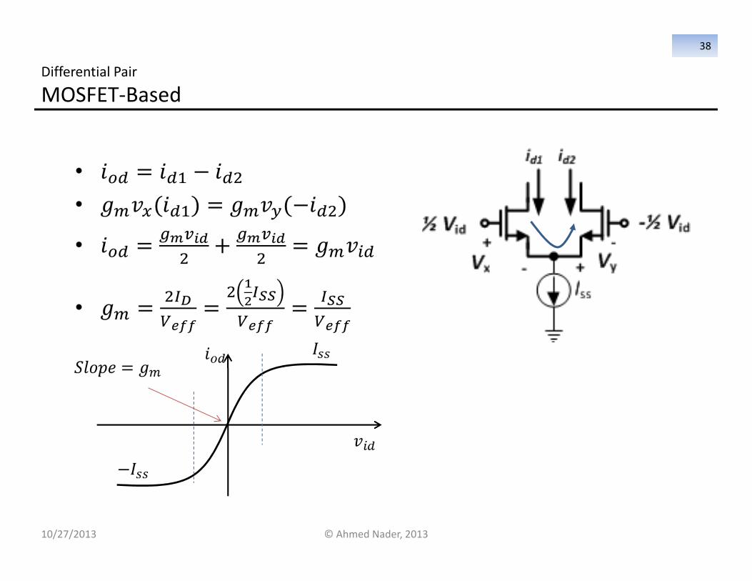
Differential Pair
10/27/2013
MOSFET-Based
© Ahmed Nader, 2013
38

Differential Pair
10/27/2013
MOSFET-Based : Large Signal
© Ahmed Nader, 2013
39

Differential Pair
10/27/2013
MOSFET-Based : Large Signal
Assignment 2d
© Ahmed Nader, 2013
40

Differential Pair
10/27/2013
MOSFET-Based : Small Signal (CMRR due to Random Mismatch)
© Ahmed Nader, 2013
41
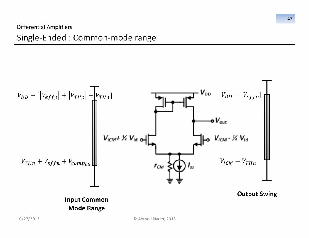
Differential Amplifiers
10/27/2013
Single-Ended : Common-mode range
Input Common
Mode Range
��� − [ ����� + �� − ��]
�� + ����� + � �����
Output Swing
���� − ��
��� − |�����|
© Ahmed Nader, 2013
42

Differential Amplifiers
10/27/2013
Single-Ended : Differential DC-gain
• �� = ���
• ���� =��
��
• � = ! + ! +��
"#$
• ���� = %�� // &'#()
*
• �+�,� = %�� 1 + ��.!
/0= 2 %��
• ���� = %�� // %��
• 2+��� = ��� (%�� // %��)
Ir
r
r
i
v
ii
i
Rdown
© Ahmed Nader, 2013
43

Differential Amplifiers
10/27/2013
Single-Ended : Common-mode DC-gain
• By symmetry, ��5 and ����6�� are equal.
• KCL @ Vo3:
– ��5 = −�7
/0$
– ����6�� = −89:0
*":0/0$
• 2�� = −!
*"�;/0$
• Common-mode Rejection Ratio (CMRR) =
|<'9==
<�;| = ���(%�� // %��) 2%����� =
/0)
/#)>/#$×
*/0$
/�;
© Ahmed Nader, 2013
44

Differential Pair
10/27/2013
Gilbert Cell
Assignment 2e:
Prove that the Gilbert cell can act as an analog multiplier
What are the conditions to work properly as an analog multiplier?
© Ahmed Nader, 2013
45