analog & mems group (amg) - anglia.com · analog & mems group (amg) introduction of a new...
TRANSCRIPT

27-November-2017 Report ID 2017-W48-SOSSHD
1
PRODUCT/PROCESS CHANGE INFORMATION
PCI AMG/17/10616
Analog & MEMS Group (AMG)
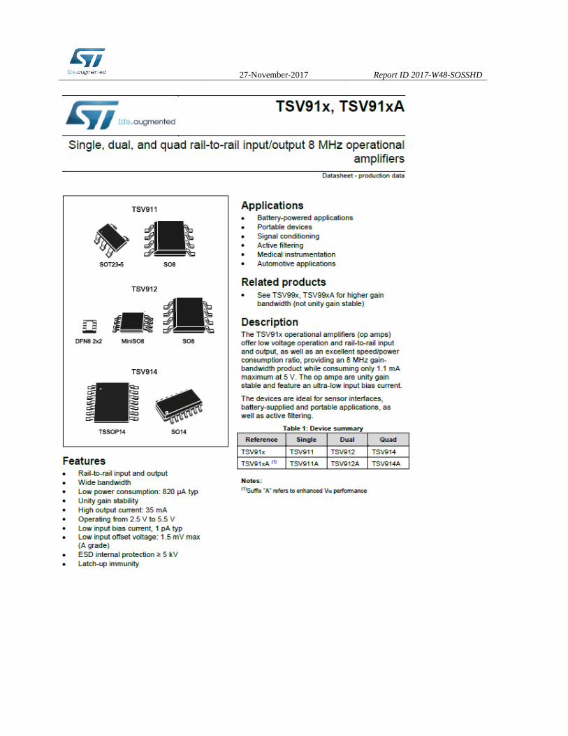
Introduction of a new Lead-frame in ST Bouskoura
for AMG products (Analog & MEMS Group) in SO8 package

27-November-2017 Report ID 2017-W48-SOSSHD
WHAT: Progressing on the activities related to our service continuous improvement, ST is glad to announce the introduction of a new Lead-frame format for AMG products in SO8 packages produced in our ST plant of Bouskoura. This minor change consists in increasing the number of unit per lead-frame. The new Super High Density lead-frame will not affect the internal structure or the plating of the lead-frame. Please find more information related to the change in the table here below
Material Current process
Modified process
Comment
Diffusion location No change
Assembly location ST Bouskoura ST Bouskoura No change
Molding compound Sumitomo G700KC Sumitomo G700KC No change
Die attach Ablestick 8601-S25 Ablestick 8601-S25 No change
Lead-frame High Density (copper) Super High density (copper) No change package internal design
Wire Copper 1 mil Copper 1 mil No change
Plating Sn Sn No change
WHY: This change will contribute to ST’s continuous service improvement and ensure a consistent assem-bly process through all the SO production lines. HOW: The qualification program consists mainly of comparative electrical characterization and reliability tests. You will find here after the qualification test plan which summarizes the various test methods and conditions that ST uses for this qualification program. WHEN: This Super High Density Lead-frame will be implemented in January 2018 in Bouskoura. Marking and traceability: Unless otherwise stated by customer’s specific requirement, the traceability of the parts assembled with the new material set will be ensured by new internal sales type, date code and lot number. The changes here reported will not affect the electrical, dimensional and thermal parameters keep-ing unchanged all the information reported on the relevant datasheets. There is -as well- no change in the packing process or in the standard delivery quantities. Shipments may start earlier with the customer’s written agreement.

27-November-2017 Report ID 2017-W48-SOSSHD
Reliability Report Lead-frame format for SO8 in
ST Bouskoura for AMG products
General Information on Test vehicles
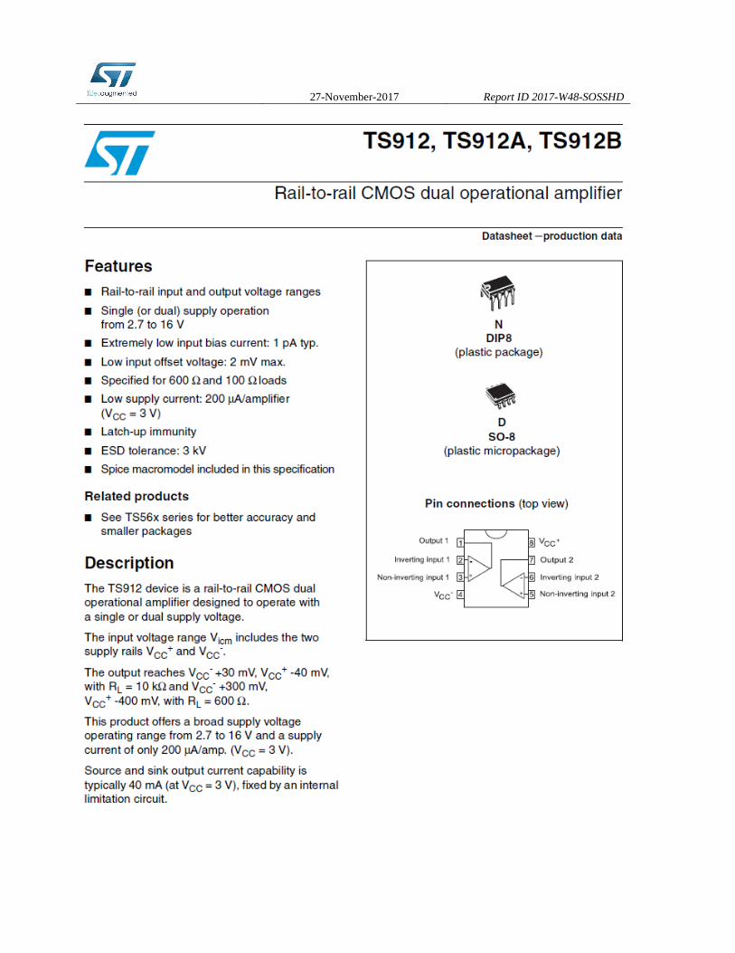
Product Line 0393, V912, 0922, 0912, UY32, UW23, 16VA, UE27, 0303, U093, UQ18
Product Description Dual comparator, Dual op amp,
P/N
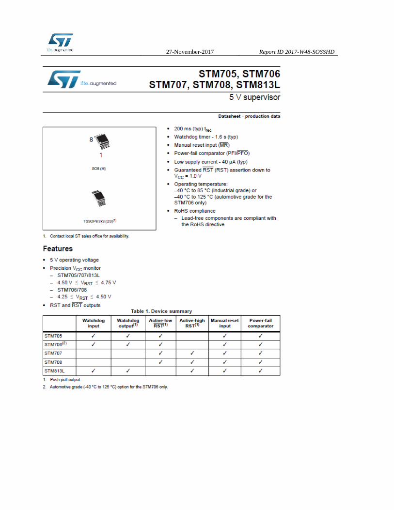
LM2903DT, TV912IDT, TS922IDT, TS912IDT, TSX922IDT, ST3485, STM706, L6562, TSM103, L6561, PM881
Product Group AMG
Product division General Purpose Analog &RF, Industrial Power Conversion
Package SO8
Silicon Process technology
Bipolar, HF5CMOS, HF2CMOS, HC1PA, HVG8A, BCD3S, HCMOS4, BCD2S, Bi-polar, BCD6, BCD6S
Locations
Wafer fab
ST Singapore UMC ST Agrate ST Catania
Assembly plant ST Bouskoura (Morocco)
Reliability Lab
ST Grenoble, ST Casteletto ST Agrate ST Catania ST Bouskoura
No change on the frame design inside the package
Current New
Note: This report is a summary of the reliability trials performed in good faith by STMicroelectronics in order to evaluate
the potential reliability risks during the product life using a set of defined test methods. This report does not imply for
STMicroelectronics expressly or implicitly any contractual obligations other than as set forth in STMicroelectronics general
terms and conditions of Sale. This report and its contents shall not be disclosed to a third party without previous written
agreement from STMicroelectronics.

27-November-2017 Report ID 2017-W48-SOSSHD
TABLE OF CONTENTS 1 APPLICABLE AND REFERENCE DOCUMENTS .......................................................................... 9 2 GLOSSARY ..................................................................................................................................... 9 3 RELIABILITY EVALUATION OVERVIEW ...................................................................................... 9
3.1 OBJECTIVES ............................................................................................................................. 9 3.2 CONCLUSION ........................................................................................................................... 9
4 DEVICE CHARACTERISTICS ...................................................................................................... 10 4.1 DEVICE DESCRIPTION ............................................................................................................. 10 4.2 CONSTRUCTION NOTE ............................................................................................................. 21
5 TESTS RESULTS SUMMARY ...................................................................................................... 22 5.1 TEST VEHICLE ........................................................................................................................ 22 5.2 TEST PLAN AND RESULTS SUMMARY ........................................................................................ 22
6 ANNEXES ...................................................................................................................................... 26 6.1 DEVICE DETAILS ..................................................................................................................... 26 6.2 TESTS DESCRIPTION .............................................................................................................. 29

27-November-2017 Report ID 2017-W48-SOSSHD
1 APPLICABLE AND REFERENCE DOCUMENTS
Document reference Short description JESD47 Stress-Test-Driven Qualification of Integrated Circuits
2 GLOSSARY DUT Device Under Test PCB Printed Circuit Board SS Sample Size
3 RELIABILITY EVALUATION OVERVIEW
3.1 Objectives To qualify the Super High Density Lead-frame in SO8 package for products manufactured in ST Bous-koura.
3.2 Conclusion Successful fulfillment of the qualification plan is required. It is stressed that reliability tests have to show that the devices behave correctly against environmental tests (no failure). Moreover, the stability of electrical parameters during the accelerated tests have to demonstrate the ruggedness of the products and safe operation, which is consequently expected during their lifetime.

27-November-2017 Report ID 2017-W48-SOSSHD
4 DEVICE CHARACTERISTICS
4.1 Device description LM2903YDT
27-November-2017 Report ID 2017-W48-SOSSHD

27-November-2017 Report ID 2017-W48-SOSSHD
27-November-2017 Report ID 2017-W48-SOSSHD

27-November-2017 Report ID 2017-W48-SOSSHD
27-November-2017 Report ID 2017-W48-SOSSHD

27-November-2017 Report ID 2017-W48-SOSSHD
27-November-2017 Report ID 2017-W48-SOSSHD

27-November-2017 Report ID 2017-W48-SOSSHD
27-November-2017 Report ID 2017-W48-SOSSHD
27-November-2017 Report ID 2017-W48-SOSSHD

27-November-2017 Report ID 2017-W48-SOSSHD
4.2 Construction note P/N
LM2903DT P/N
TSV912IDT P/N
TS922IDT P/N
TS912IDT P/N
TL431AIDT Wafer/Die fab. information Wafer fab manufacturing location ST Singapore UMC taiwan ST Singapore ST Singapore ST Singapore Technology Bipolar HF5CMOS HF2CMOS HC1PA HBIP40 Die finishing back side RAW SILICON RAW SILICON RAW SILICON RAW SILICON RAW SILICON Die size (microns) 950 x 870 µm 1100x1070µm 1720x1190µm 2600x1950 0,9x0,62 Bond pad metallization layers AlSiCu AlCu AlSiCu AlSi AlSiCu Passivation type Nitride Nitride Nitride PVAPOX+Nitride PVAPOX+Nitride
Assembly information Assembly site ST Bouskoura ST Bouskoura ST Bouskoura ST Bouskoura ST Bouskoura Package description SO8 SO8 SO8 SO8 SO8 Molding compound EME G700KC EME G700KC EME G700KC EME G700KC EME G700KC Frame material Cu Cu Cu Cu Cu Die attach process Epoxy Glue Epoxy Glue Epoxy Glue Epoxy Glue Epoxy Glue Die attach material 8601S-25 8601S-25 8601S-25 8601S-25 8601S-25 Wire bonding process Thermosonic ball
bonding Thermosonic ball bon-
ding Thermosonic ball bonding Thermosonic ball bonding Thermosonic ball bon-
ding Wires bonding materials/diameters Cu 1 mil Cu 1 mil Cu 1 mil Cu 1 mil Cu 1 mil Lead finishing process electroplating electroplating electroplating electroplating electroplating Lead finishing/bump solder mate-rial
Matte tin Matte tin Matte tin Matte tin Matte tin
P/N
TSX922IDT P/N
ST3485EIDT P/N
STM706M7F P/N
L6562 P/N
TSM103 Wafer/Die fab. information Wafer fab manufacturing location ST Agrate ST Singapore ST Singapore ST Singapore ST Singapore Technology HVG8A BCD3S HCMOS4 BCD2S Bipolar Die finishing back side Raw silicon Raw silicon Raw silicon CHROMIUM/NICKEL Raw silicon Die size (microns) 1700x1400µm² 1950x2720 µm² 1350x1510 µm² 1790x1870 µm² 1890x2120 µm² Bond pad metallization layers AlCu AlSi AlSiCu AlSiCu AlSiCu Passivation type HDP/TEOS/SiN/Polyimide PVAPOX/
NITRIDE/POLYIMIDE PVAPOX+Nitride SiN/Poly SiN/Poly
Assembly information Assembly site ST Bouskoura ST Bouskoura ST Bouskoura ST Bouskoura ST Bouskoura Package description SO8 SO8 SO8 SO8 SO8 Molding compound EME G700KC EME G700KC EME G700KC EME G700KC EME G700KC Frame material Cu Cu Cu Cu Cu Die attach process Epoxy Glue Epoxy Glue Epoxy Glue Epoxy Glue Epoxy Glue Die attach material 8601S-25 8601S-25 8601S-25 8601S-25 8601S-25 Wire bonding process Thermosonic ball bonding Thermosonic ball bon-
ding Thermosonic ball bonding Thermosonic ball bonding Thermosonic ball bon-
ding Wires bonding materials/diameters Cu 1 mil Cu 1 mil Cu 1 mil Cu 1 mil Cu 1 mil Lead finishing process electroplating electroplating electroplating electroplating electroplating Lead finishing/bump solder material Matte tin Matte tin Matte tin Matte tin Matte tin
P/N
L6561D013TR Wafer/Die fab. information Wafer fab manufacturing location ST Singapore Technology BCD6 Die finishing back side CHROMIUM/NICKEL/GOLD Die size (microns) 2590x2060 µm² Bond pad metallization layers AlSi Passivation type SiN
Assembly information Assembly site ST Bouskoura Package description SO8 Molding compound EME G700KC Frame material Cu Die attach process Epoxy Glue Die attach material 8601S-25 Wire bonding process Thermosonic ball bonding Wires bonding materials/diameters Cu 1 mil Lead finishing process electroplating Lead finishing/bump solder material Matte tin
27-November-2017 Report ID 2017-W48-SOSSHD
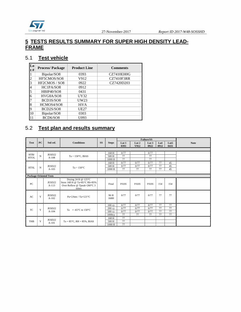
5 TESTS RESULTS SUMMARY FOR SUPER HIGH DENSITY LEAD-FRAME
5.1 Test vehicle Lot #
Process/ Package Product Line Comments
1 Bipolar/SO8 0393 CZ7410EH0G 2 HF5CMOS/SO8 V912 CZ7410F3RR 3 HF2CMOS / SO8 0922 CZ7420D203 4 HC1PA/SO8 0912 5 HBIP40/SO8 0431 6 HVG8A/SO8 UY32 7 BCD3S/SO8 UW23 8 HCMOS4/SO8 16VA 9 BCD2S/SO8 UE27 10 Bipolar/SO8 0303 11 BCD6/SO8 U093
5.2 Test plan and results summary
Test PC Std ref. Conditions SS Steps Failure/SS
Lot 1 0393
Lot 2 V912
Lot 3 0922
Lo4 0912
Lot5 0431
Note
HTB/ HTOL
N JESD22 A-108
Ta = 150°C, BIAS 168 H 0/77 0/77 500 H 77 77 1000 H 77 77
HTSL N JESD22 A-103
Ta = 150°C
168 H 0/77 0/77 0/77 77 45 500 H 0/77 0/77 0/77 77 45
1000 H 77 77 77 77 45
Package Oriented Tests
PC JESD22 A-113
Drying 24 H @ 125°C Store 168 H @ Ta=85°C Rh=85% Over Reflow @ Tpeak=260°C 3
times
Final PASS PASS PASS 154 154
AC Y JESD22 A-102
Pa=2Atm / Ta=121°C 96 H 168H
0/77
0/77
0/77
77
77
TC Y JESD22 A-104
Ta = -65°C to 150°C
100 cy 0/77 0/77 0/77 77 77 200 cy 0/77 0/77 0/77 77 77 500 cy 0/77 0/77 0/77 77 77 1000cy 77 77 77 77 77
THB Y JESD22 A-101
Ta = 85°C, RH = 85%, BIAS 168 H 77 500 H 77 1000 H 77
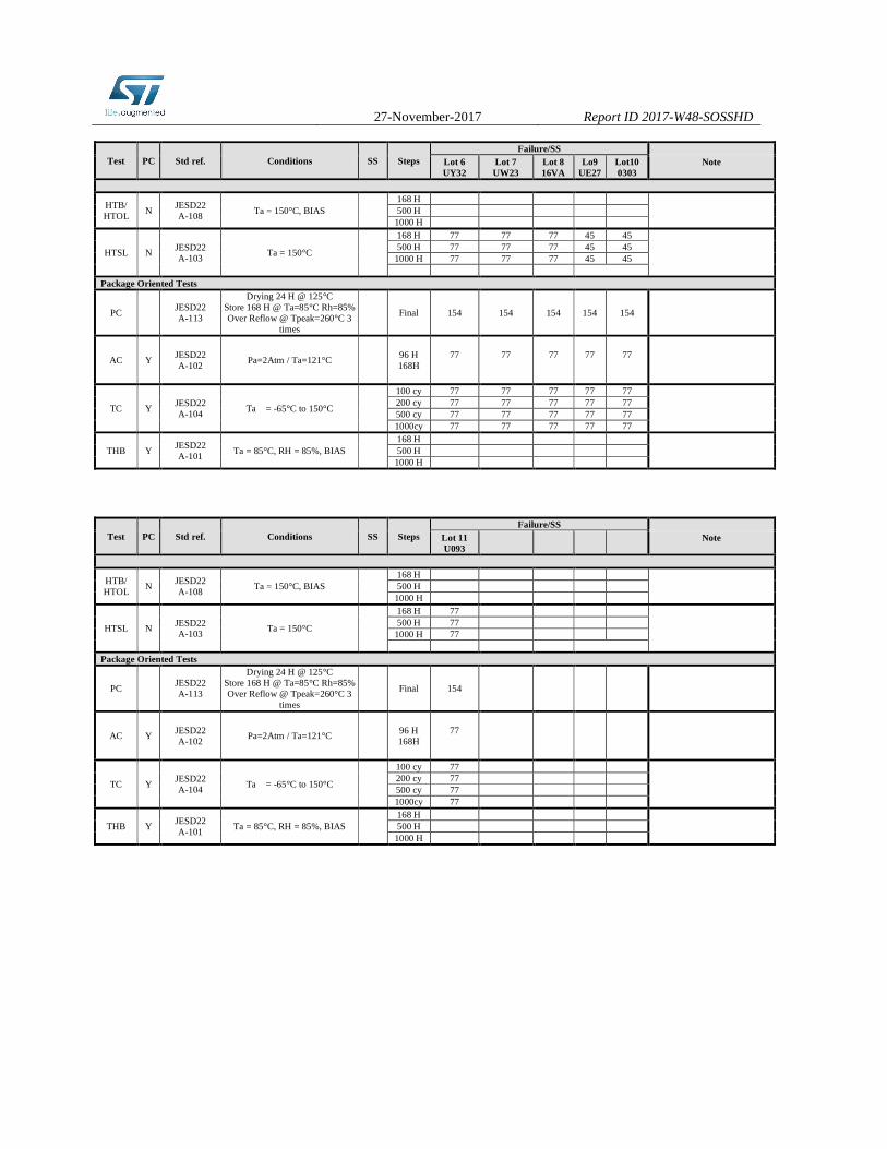
27-November-2017 Report ID 2017-W48-SOSSHD
Test PC Std ref. Conditions SS Steps Failure/SS
Lot 6 UY32
Lot 7 UW23
Lot 8 16VA
Lo9 UE27
Lot10 0303
Note
HTB/ HTOL
N JESD22 A-108
Ta = 150°C, BIAS 168 H 500 H 1000 H
HTSL N JESD22 A-103
Ta = 150°C
168 H 77 77 77 45 45 500 H 77 77 77 45 45
1000 H 77 77 77 45 45
Package Oriented Tests
PC JESD22 A-113
Drying 24 H @ 125°C Store 168 H @ Ta=85°C Rh=85% Over Reflow @ Tpeak=260°C 3
times
Final 154 154 154 154 154
AC Y JESD22 A-102
Pa=2Atm / Ta=121°C 96 H 168H
77
77
77
77
77
TC Y JESD22 A-104
Ta = -65°C to 150°C
100 cy 77 77 77 77 77 200 cy 77 77 77 77 77 500 cy 77 77 77 77 77 1000cy 77 77 77 77 77
THB Y JESD22 A-101
Ta = 85°C, RH = 85%, BIAS 168 H 500 H 1000 H
Test PC Std ref. Conditions SS Steps Failure/SS
Lot 11 U093
Note
HTB/ HTOL
N JESD22 A-108
Ta = 150°C, BIAS 168 H 500 H 1000 H
HTSL N JESD22 A-103
Ta = 150°C
168 H 77 500 H 77
1000 H 77
Package Oriented Tests
PC JESD22 A-113
Drying 24 H @ 125°C Store 168 H @ Ta=85°C Rh=85% Over Reflow @ Tpeak=260°C 3
times
Final 154
AC Y JESD22 A-102
Pa=2Atm / Ta=121°C 96 H 168H
77
TC Y JESD22 A-104
Ta = -65°C to 150°C
100 cy 77 200 cy 77 500 cy 77 1000cy 77
THB Y JESD22 A-101
Ta = 85°C, RH = 85%, BIAS 168 H 500 H 1000 H

27-November-2017 Report ID 2017-W48-SOSSHD
Just for your reference, please find here below the results of the Current High density Lead-frame (with the same material set)
P/N
LM2903YDT P/N
LM2901YDT P/N
TL084IYDT P/N
ST3485EIYDT P/N
TS924IDT Wafer/Die fab. information Wafer fab manufacturing loca-tion
ST Singapore ST Singapore ST Singapore ST Singapore ST Singapore
Technology Bipolar Bipolar JFet BCD3S HF2CMOS Die finishing back side RAW SILICON RAW SILICON RAW SILICON RAW SILICON RAW SILICON Die size (microns) 950 x 870 µm 1370x1270 2480 x 1460 1950x2720 1980x2450 Bond pad metallization layers AlSiCu AlSiCu AlSiCu AlSi AlSiCu Passivation type Nitride Nitride P-VAPOX/NITRIDE P-VAPOX/NITRIDE/POLYIMIDE P-VAPOX/NITRIDE
Wafer Testing (EWS) informa-tion
Electrical testing manufacturing location
ST Singapore ST Singapore ST Singapore ST Singapore
ST Singapore
Tester ASL1K ASL1K ASL1K ASL1K ASL1K
Assembly information Assembly site ST Bouskoura ST Bouskoura ST Bouskoura ST Bouskoura ST Bouskoura Package description SO8 SO14 SO14 SO8 SO14 Molding compound EME G700KC EME G700KC EME G700KC EME G700KC EME G700KC Frame material Cu Cu Cu Cu Cu Die attach process Epoxy Glue Epoxy Glue Epoxy Glue Epoxy Glue Epoxy Glue Die attach material 8601S-25 8601S-25 8601S-25 8601S-25 8601S-25 Wire bonding process Thermosonic ball bon-
ding Thermosonic ball bon-
ding Thermosonic ball bonding Thermosonic ball bonding Thermosonic ball bonding
Wires bonding materials/diame-ters
Cu 1 mil Cu 1 mil Cu 1 mil Cu 1 mil Cu 1 mil
Lead finishing process electroplating electroplating electroplating electroplating electroplating Lead finishing/bump solder ma-terial
Matte tin Matte tin Matte tin Matte tin Matte tin
Final testing information Testing location ST Bouskoura ST Bouskoura ST Bouskoura ST Bouskoura ST Bouskoura Tester ASL1K ASL1K ASL1K ASL1K ASL1K
P/N
TSX3704IYDT P/N
TSX3702IYDT P/N
STM706YM7F P/N
MC33079YDT P/N
TS912IYDT P/N
TSV912IYDT Wafer/Die fab. infor-mation
Wafer fab manufactu-ring location
ST Agrate ST Agrate ST Singapore ST Singapore ST Singapore UMC
Technology HVG8A HVG8A HCMOS4 Bipolar HC1PA HF5CMOS Die finishing back side RAW SILICON RAW SILICON RAW SILICON RAW SILICON RAW SILICON RAW SILICON Die size (microns) 1830x1440 µm 1018x1238 µm 1350 x 1510µm 3230x1950µm 2600x1950µm 1100x1070µm Bond pad metallization layers
AlCu AlCu AlSiCu AlSiCu AlSi AlCu
Passivation type HDP/TEOS/SiN/Polyimide HDP/TEOS/SiN/Polyimide PSG+Silicon Nitride+Po-lyimide
Nitride PVAPOX+Nitride Nitride
Wafer Testing (EWS) information
Electrical testing manu-facturing location
ST Singapore ST Singapore ST Singapore ST Singapore ST Singapore ST Singapore
Tester ASL1K ASL1K ASL1K ASL1K ASL1K ASL1K
Assembly information Assembly site ST Bouskoura ST Bouskoura ST Bouskoura ST Bouskoura ST Bouskoura ST Bouskoura Package description SO14 SO14 SO8 SO14 SO8 SO8 Molding compound EME G700KC EME G700KC EME G700KC EME G700KC EME G700KC EME G700KC Frame material Cu Cu Cu Cu Cu Cu Die attach process Epoxy Glue Epoxy Glue Epoxy Glue Epoxy Glue Epoxy Glue Epoxy Glue Die attach material 8601S-25 8601S-25 8601S-25 8601S-25 8601S-25 8601S-25 Wire bonding process Thermosonic ball bonding Thermosonic ball bonding Thermosonic ball bonding Thermosonic ball bon-
ding Thermosonic ball
bonding Thermosonic ball bonding
Wires bonding mate-rials/diameters
Cu 1 mil Cu 1 mil Cu 1 mil Cu 1 mil Cu 1 mil Cu 1 mil
Lead finishing process electroplating electroplating electroplating electroplating electroplating electroplating Lead finishing/bump solder material
Matte tin Matte tin Matte tin Matte tin Matte tin Matte tin
Final testing informa-tion
Testing location ST Bouskoura ST Bouskoura ST Bouskoura ST Bouskoura ST Bouskoura ST Bouskoura
27-November-2017 Report ID 2017-W48-SOSSHD
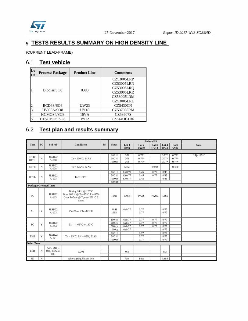
6 TESTS RESULTS SUMMARY ON HIGH DENSITY LINE
(CURRENT LEAD-FRAME)
6.1 Test vehicle Lot # Process/ Package Product Line Comments
1 Bipolar/SO8 0393
CZ53005LRP CZ53005LRN CZ53005LRQ CZ53005LRR CZ53005LRM CZ53005LRL
2 BCD3S/SO8 UW23 CZ5430CN 3 HVG8A/SO8 UY18 CZ537088RM 4 HCMOS4/SO8 16VA CZ53607S 5 HF5CMOS/SO8 V912 CZ544OC1RR
6.2 Test plan and results summary
Test PC Std ref. Conditions SS Steps Failure/SS
Lot 1 0393
Lot 2 UW23
Lot 3 UY18
Lot 4 16VA
Lot5 V912
Note
HTB/ HTOL
N JESD22 A-108
Ta = 150°C, BIAS 168 H 0/78 0/77* 0/77* 0/77* * Tj=125°C 500 H 0/78 0/77* 0/77* 0/77* 1000 H 0/78 0/77* 0/77* 0/77*
ELFR N JESD22 A-008
Ta = 125°C, BIAS 0/450 0/450 0/450
HTSL N JESD22 A-103
Ta = 150°C
168 H 6X0/77 0/45 0/77 0/45 500 H 6X0/77 0/45 0/77 0/45 1000 H 6X0/77 0/45 0/45 2000H
Package Oriented Tests
PC JESD22 A-113
Drying 24 H @ 125°C Store 168 H @ Ta=85°C Rh=85% Over Reflow @ Tpeak=260°C 3
times
Final PASS PASS PASS PASS
AC Y JESD22 A-102
Pa=2Atm / Ta=121°C 96 H 168H
6x0/77
0/77 0/77
0/77 0/77
TC Y JESD22 A-104
Ta = -65°C to 150°C
100 cy 6x0/77 0/77 0/77 0/77 200 cy 6x0/77 0/77 0/77 0/77 500 cy 6x0/77 0/77 0/77 0/77 1000cy 6x0/77 0/77
THB Y JESD22 A-101
Ta = 85°C, RH = 85%, BIAS 168 H 0/77 0/77 500 H 0/77 0/77 1000 H 0/77 0/77
Other Tests
ESD N AEC Q101-001, 002 and
005
CDM 0/3 0/3
SD N After ageing 8h and 16h Pass Pass PASS
27-November-2017 Report ID 2017-W48-SOSSHD
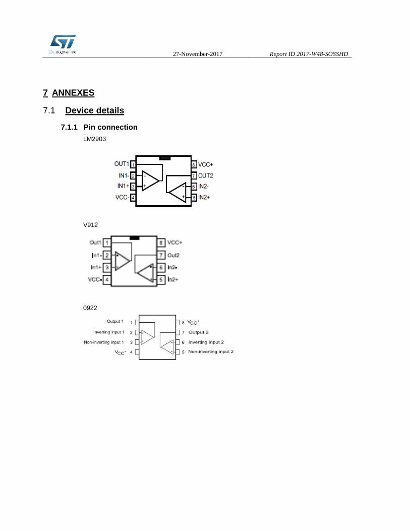
7 ANNEXES
7.1 Device details
7.1.1 Pin connection
LM2903
V912
0922
27-November-2017 Report ID 2017-W48-SOSSHD
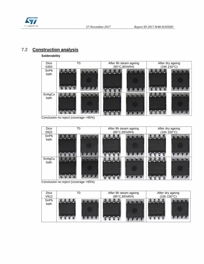
7.2 Construction analysis Solderability
Dice 0393
T0 After 8h steam ageing (85°C,85%RH)
After dry ageing (16h 150°C)
SnPb bath
SnAgCu
bath
Conclusion no reject (coverage >95%)
Dice 0922
T0 After 8h steam ageing (85°C,85%RH)
After dry ageing (16h 150°C)
SnPb bath
SnAgCu
bath
Conclusion no reject (coverage >95%)
Dice V912
T0 After 8h steam ageing (85°C,85%RH)
After dry ageing (16h 150°C)
SnPb bath
27-November-2017 Report ID 2017-W48-SOSSHD
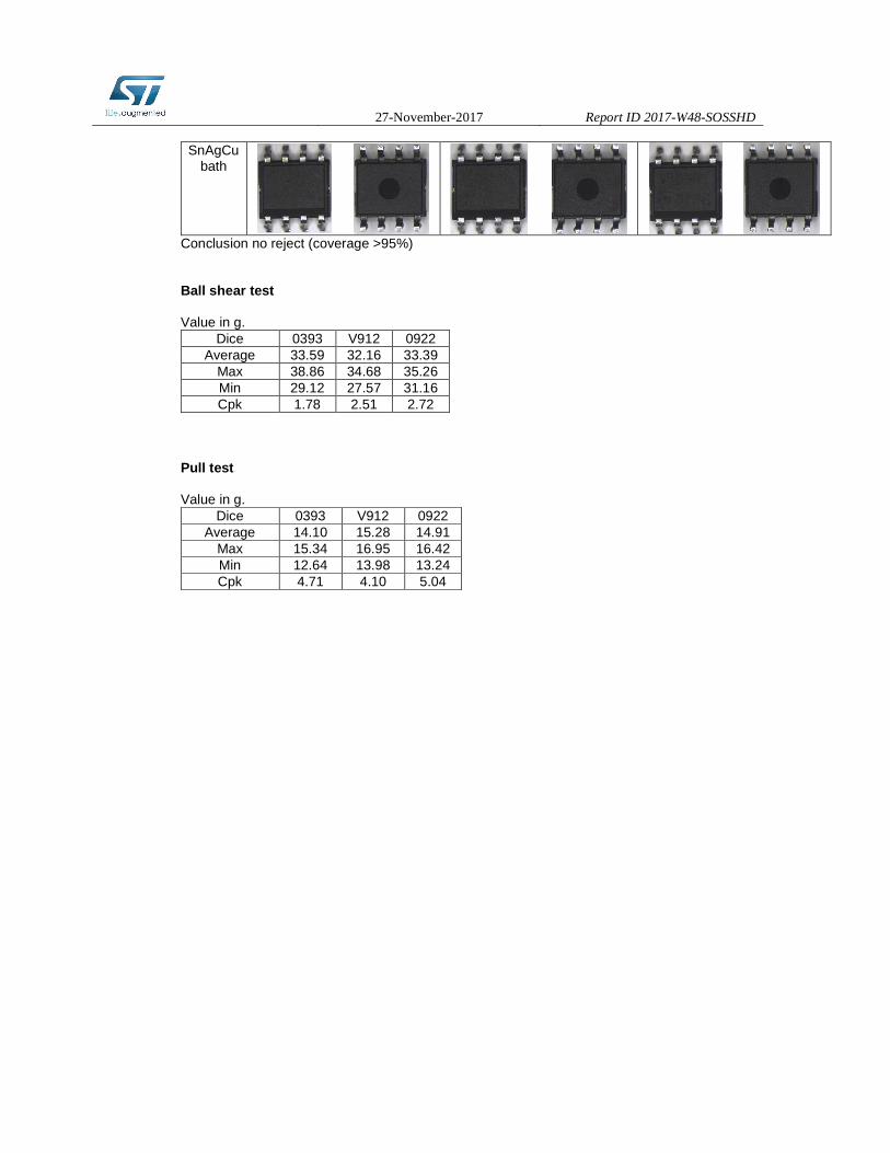
SnAgCu bath
Conclusion no reject (coverage >95%) Ball shear test Value in g.
Dice 0393 V912 0922 Average 33.59 32.16 33.39
Max 38.86 34.68 35.26 Min 29.12 27.57 31.16 Cpk 1.78 2.51 2.72
Pull test Value in g.
Dice 0393 V912 0922 Average 14.10 15.28 14.91
Max 15.34 16.95 16.42 Min 12.64 13.98 13.24 Cpk 4.71 4.10 5.04

27-November-2017 Report ID 2017-W48-SOSSHD
7.3 Tests Description
Test name Description Purpose Die Oriented
HTOL High Temperature
Operating Life
HTB High Temperature
Bias
The device is stressed in static or dynamic configuration, approaching the operative max. absolute ratings in terms of junction temperature and bias condition.
To determine the effects of bias conditions and temperature on solid state devices over time. It simulates the devices’ operating con-dition in an accelerated way. The typical failure modes are related to, sili-con degradation, wire-bonds degradation, ox-ide faults.
HTRB High Temperature
Reverse Bias
HTFB / HTGB High Temperature
Forward (Gate) Bias
The device is stressed in static configura-tion, trying to satisfy as much as possible the following conditions: low power dissipation; max. supply voltage compatible with diffu-sion process and internal circuitry limita-tions;
To determine the effects of bias conditions and temperature on solid state devices over time. It simulates the devices’ operating con-dition in an accelerated way. To maximize the electrical field across either reverse-biased junctions or dielectric layers, in order to investigate the failure modes linked to mobile contamination, oxide ageing, layout sensitivity to surface effects.
HTSL High Temperature
Storage Life
The device is stored in unbiased condition at the max. temperature allowed by the pack-age materials, sometimes higher than the max. operative temperature.
To investigate the failure mechanisms acti-vated by high temperature, typically wire-bonds solder joint ageing, data retention faults, metal stress-voiding.
ELFR Early Life Failure
Rate
The device is stressed in biased conditions at the max junction temperature.
To evaluate the defects inducing failure in early life.
Package Oriented
PC Preconditioning
The device is submitted to a typical temper-ature profile used for surface mounting de-vices, after a controlled moisture absorption.
As stand-alone test: to investigate the moisture sensitivity level. As preconditioning before other reliability tests: to verify that the surface mounting stress does not impact on the subsequent reliability performance. The typical failure modes are "pop corn" ef-fect and delamination.
AC Auto Clave (Pres-
sure Pot)
The device is stored in saturated steam, at fixed and controlled conditions of pressure and temperature.
To investigate corrosion phenomena affecting die or package materials, related to chemical contamination and package hermeticity.
TC Temperature Cy-
cling
The device is submitted to cycled tempera-ture excursions, between a hot and a cold chamber in air atmosphere.
To investigate failure modes related to the thermo-mechanical stress induced by the dif-ferent thermal expansion of the materials in-teracting in the die-package system. Typical failure modes are linked to metal displace-ment, dielectric cracking, molding compound delamination, wire-bonds failure, die-attach layer degradation.
27-November-2017 Report ID 2017-W48-SOSSHD
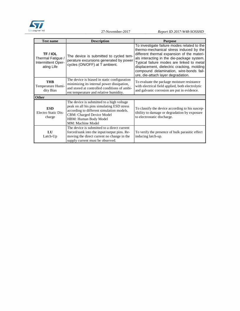
Test name Description Purpose
TF / IOL Thermal Fatigue / Intermittent Oper-
ating Life
The device is submitted to cycled tem-perature excursions generated by power cycles (ON/OFF) at T ambient.
To investigate failure modes related to the thermo-mechanical stress induced by the different thermal expansion of the materi-als interacting in the die-package system. Typical failure modes are linked to metal displacement, dielectric cracking, molding compound delamination, wire-bonds fail-ure, die-attach layer degradation.
THB Temperature Humi-
dity Bias
The device is biased in static configuration minimizing its internal power dissipation, and stored at controlled conditions of ambi-ent temperature and relative humidity.
To evaluate the package moisture resistance with electrical field applied, both electrolytic and galvanic corrosion are put in evidence.
Other
ESD Electro Static Dis-
charge
The device is submitted to a high voltage peak on all his pins simulating ESD stress according to different simulation models. CBM: Charged Device Model HBM: Human Body Model MM: Machine Model
To classify the device according to his suscep-tibility to damage or degradation by exposure to electrostatic discharge.
LU Latch-Up
The device is submitted to a direct current forced/sunk into the input/output pins. Re-moving the direct current no change in the supply current must be observed.
To verify the presence of bulk parasitic effect inducing latch-up.