analysis and control of two switches ac chopper voltage ... · snubber circuit. the over-voltage...
TRANSCRIPT
Analysis and Control of Two Switches AC Chopper Voltage Regulator
Jin Nan1,2, Tang Hou-Jun1, Bai Liang-Yu1, Geng Xin1 Yang Xiao-Liang2 School of Electronic, Information and Electrical Engineering1 School of Electrical Engineering2
Shanghai Jiao Tong University Zhengzhou University of Light Industry Shanghai Zhengzhou, Henan China China
jinnan, hjtang, bailiangyu, [email protected] [email protected] Abstract: - In this paper, an improved topology of Buck type AC chopper voltage regulator and its control strategy are proposed. This converter only using two power switches is low cost, easy implemented and the phase synchronized circuit is not needed. The current path is provided in dead-time period by using simple snubber circuit. The over-voltage protection varistor is also applied to absorb the voltage spikes which may destroy the power switches. The voltage spikes in dead-time mode commutation are greatly reduced and the power switches are protected. Furthermore, the feedforward and feedback control strategy is proposed to suppress fluctuations and eliminate the harmonic components caused by power quality problems of the input voltage. The proposed converter could realize wide range voltage regulation with high power transfer efficiency and low total harmonic distortion. The steady-state equivalent circuit and the input power factor are derived through theoretical analysis. The output filter design method is also presented. Based on the theoretical analysis and calculation, an experimental prototype is setup. The simulation and experiment results verify the validity of the proposed design.
Key-Words: AC chopper, Voltage Regulator, Pulse Width Modulation, Feedforward and Feedback Control, Power Factor, Voltage Fluctuations
1 Introduction AC chopper converter has been widely used in automatic voltage regulators [1-3], soft-starter and speed regulator of the inductor motor [4-6], light dimmer [7] and so on. There are some kinds of AC voltage regulators such as auto-transformer and thyristor phase-controlled voltage regulator. Auto-transformer has a large size and its voltage regulating speed is low. The thyristor phase controlled voltage regulator has a relatively fast response compared with the auto-transformer[8]. However, the low input power factor and large amount of the low-order harmonic currents are the major problems. Large passive filter is needed and the system cost is increased.
These problems can be solved by using PWM AC chopper. This chopper converter has some advantages such as high input power factor, fast dynamics and small size filter. Three switches [9,10] and four switches [11-15] AC chopper are presented in the previous presented papers. In these researches, the switching patterns are critical and an alternate path has to be established in dead-time period. DC regenerative snubber capacitor [1,7,11] was used to realize safe commutation and enhance efficiency. However, these converters still have complex topologies and control strategies. These commutation strategies are related to the phase of
input voltage, input current or inductor current. As a result, these converters are prone to be disturbed and hard to be implemented. In addition, there are voltage spikes across the power switches during the commutation process. The previous researches have not given enough consideration to the protection of the power switches. Thus, the switching devices are easy to be destroyed for lack of protection.
In this paper, a buck type ac chopper voltage regulator with snubber circuit is proposed. The bilateral switch is composed of an Insulated Gate Bipolar Transistor(IGBT) and a fast recovery diode rectifier. Only two switching devices are used instead of three or four switches in the previous presented plans. Thus, cost is reduced and commutation process is highly simplified. The simple and effective snubber circuit consists of an absorbing circuit and an over-voltage protection varistor. When the two switches are both switched off, they provide a current way to avoid high voltage spikes. Therefore, the voltage spikes are reduced and safe commutation is realized.
Based on the analysis of working principle and commutation process, the equivalent circuit and the input power factor of the proposed converter are derived. The calculation methods of main component parameters are also investigated.
WSEAS TRANSACTIONS on CIRCUITS and SYSTEMSJin Nan, Tang Hou-Jun, Bai Liang-Yu, Geng Xin, Yang Xiao-Liang
ISSN: 1109-2734 208 Issue 4, Volume 9, April 2010

The harmonic components and fluctuations in the input voltage can also affect the quality of the output voltage. In previous researches [6,9], peak voltage or root-mean-square(RMS) voltage were used as the controller input. These signals change only one time in each period of the input voltage. Thus, the low dynamic response speed is the major problem. In addition, the harmonic voltage problems caused by input voltage have not been investigated. Therefore, in order to keep the output voltage stable, a voltage feedforward and feedback control strategy is proposed. This control strategy adopts instantaneous voltage as the controller input. The output voltage can be stabilized and the dynamic response speed is improved. Furthermore, the proposed control strategy not only can suppress the voltage fluctuations but also eliminate the harmonic components caused by input voltage quality problems. As a result, this voltage regulator has many advantages such as simple structure, easy implementation, high input power factor, small size filter, low total harmonic distortion and high power transfer efficiency. A prototype is set up based on the theoretical analysis and calculation. The simulation and experiment results verified the validity of the proposed plan.
2 Description of the converter There are several types of the ac chopper converter. A two switches topology is adopted and the snubber circuits are designed to ensure safe commutation. The converter topology and commutation strategy are discussed as follows. 2.1 Converter topology
The basic structure of the proposed converter is shown in Fig.1. This Buck type AC Chopper is powered by the source voltage ui. Inductor Li and capacitor Ci construct the input filter to absorb the harmonic currents. S1 and S2 are bilateral switches which are composed of IGBTs and fast recovery diode rectifiers. This bilateral switch structure is shown in Fig.1.b. Compared to other bilateral switch structures, it only uses one IGBT. Thus, the driver circuit is simplified and the cost is reduced. These two switches work in complementary mode. In order to avoid the two switches are on states simultaneously, there is a small dead-time period. In dead-time, the two switches are both switched off. Thus, the inductor current is cut off. The inductive load or output filter inductor will produce voltage spikes across the switches. In switching process, this
voltage spikes will increase the switching losses and reduce the power transfer efficiency. Moreover, the switching devices may be destroyed by high voltage spikes. In previous researches, four switches converter and corresponding commutation strategy are designed to reduce voltage spikes [15].
In this paper, the snubber circuits are added to the power circuit to solve this problem. The snubber circuits are composed of absorbing circuits and over-voltage protection varistors. The absorbing circuit adopts a resistor connected in series with a capacitor to absorb the voltage spikes in dead-time period. However, the absorbing circuit may not absorb the voltage spikes completely. When load is highly inductive or the output current is high, the voltage spikes may destroy the switches directly. On this occasion, the over-voltage protection varistor is necessary for the safety of the switches. This snubber circuit design can solve the problems caused by the voltage spikes in switching process and ensure the safety of the converter. The output filter inductor L is used to store and transfer the energy to the output side. The output filter capacitor Co reduces the output voltage ripple.
iuiC 2S
L
OC LR
ii
Li
ou
1aC
iL1S
1aR
1pR
2pR2aR
2aC
OZ
Lu
cpu
(a)
(b)
Fig. 1 - (a) The topology of two switches Buck type AC chopper voltage regulator (b) the structure of bilateral switch
WSEAS TRANSACTIONS on CIRCUITS and SYSTEMSJin Nan, Tang Hou-Jun, Bai Liang-Yu, Geng Xin, Yang Xiao-Liang
ISSN: 1109-2734 209 Issue 4, Volume 9, April 2010

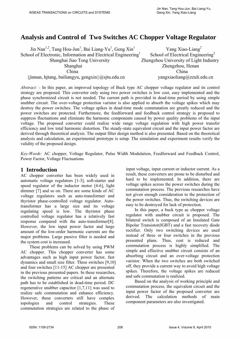
2.2 Commutation strategy The voltage regulation function of ac chopper converter is realized by using PWM techniques to the switching devices. The main operation modes are defined as: active mode and freewheeling mode. For the sake of the safe commutation, dead-time mode is added. The PWM control signals are shown in Fig.2.
us
t
Sg1
Sg2t
t
td
tSkT ( 1) Sk T
t
( ) Sk D T
Sg1
Sg2
Fig. 2 - The PWM control signals of the bilateral switches S1 and S2
Sg1 and Sg2 are the gate signals of S1 and S2. The designed PWM signals work in the complementary mode. The commutation strategy has no relation with the phase of the input voltage or input current. Therefore, the phase synchronized circuit is not needed in this system. This commutation strategy not only simplifies the hardware design, but also avoids the phase detector errors. For example, in previous researches [12,13,15], the PWM signals are controlled by the input voltage phase. When the input voltage contains harmonic components, the phase detector will be disturbed. Thus, the input voltage phase signal is not accurate. Because Sg1 and Sg2 are controlled by the input voltage phase. The disturbed PWM control signals will make the voltage regulator work unstable. Another filter circuit must be designed to ensure that the harmonic components can be eliminated, and the phase detector can work without harmonic disturbance. The phase detector will make the system complex. As a result, commutation strategy used in this paper has advantages such as easy implementation, low cost and high stability.
As the switching frequency fS is much higher than the input voltage frequency f, the input voltage
ui and the output voltage uo can be considered as a constant value in switching period. When ui>0, the operation modes and commutation strategy will be discussed as follows.
In kTS ~ (k+D)TS, S1 is switched on. The AC chopper converter works in active mode. As shown in Fig.3(a), the current path is ui-Li-S1-L-RL. In this mode, the inductor L stores the energy and the current iL increases. The intermediate chopper voltage ucp is equal to ui. In active mode, the power flows from the voltage source to the load.
1pR
suiC
2S
L
OC LR
ouoi
1aC
iL 1S
1aR
2pR2aR
2aC
(a)
suiC
2S
L
OC LR
ouoi
1aC
iL 1S
1aR1pR
2pR2aR
2aC
(b)
suiC
2S
L
OC LR
ou
oi
1aC
iL 1S
1aR1pR
2pR2aR
2aC
(c) Fig.3 - The commutation process of ac voltage regulator (a) in active mode (b) in dead-time mode (c) in freewheeling mode
Ideally, at (k+D)TS, S1 is switched off and S2
should be switched on. However, for the sake of the safe commutation and protecting the switching devices, there is a small dead-time period. In this
WSEAS TRANSACTIONS on CIRCUITS and SYSTEMSJin Nan, Tang Hou-Jun, Bai Liang-Yu, Geng Xin, Yang Xiao-Liang
ISSN: 1109-2734 210 Issue 4, Volume 9, April 2010
period, S1 and S2 are both switched off. In (k+D)TS
~(k+D)TS+td, S1 and S2 are both switched off and the converter works in dead-time mode. In dead-time mode, there will be voltage spikes caused by the cut off of the inductor current. These voltage spikes may destroy S2 or cause high switching losses. The absorbing circuit composed of Ra1 and Ca1 reduces the voltage spikes. As shown in Fig.3(b), the current path is us-Li-Ra1-Ca1-L-RL. When voltage surges, high voltage spikes or other potential over-voltage problems occur, the over-voltage protection varistor Rp1, Rp2 can protect the switching devices.
At (k+D)TS+td, S2 is switched on. In (k+D)TS+td
~(k+1)TS, S1 is off and S2 is on. The inductor current freewheels through the load and S2. The current path is S2-L-RL shown in Fig.3(c). The inductor L transfers the energy from the inductor to the load side. In this period, the converter works in freewheeling mode.
3 System analysis and calculation To simplify the analysis and calculation, the following assumptions are made: 1 Because the dead-time td is short, only 1~2μs. The energy stored in inductor is assumed to be constant in dead-time mode. This mode is ignored in the calculation of the main component parameters. 2 Input LC filter absorbs the high frequency input harmonic currents. As the switching frequency fS is much higher than the input voltage frequency f, the input power factor is assumed not to be affected by the input filter.
The voltage source ui is defined as: sin( )i imu V t (1) where ω and Vim are the angular frequency and the amplitude of the input voltage respectively.
Theoretically, the intermediate chopper voltage ucp can be expressed as:
1
10i
cp
u S is onu
S is off
(2)
The PWM switching function of S1 is expressed as:
1 ( )( )
0 ( ) ( 1)S S
S S
kT t k D Tg t k N
k D T t k T
(3)
where TS and D are switching period and duty ratio of the PWM control signal respectively. The fourier series of g(t) with a switching frequency ωS is :
1
2sin( ) cos( )S
k
kDg t D k t
k
(4)
Therefore, ucp is given by:
1
( ) ( )
sin( )sin( ) sin( )
cp i
imim S
k
u g t u t
V kDDV wt k t
k
(5) The first term of the right-hand side of equation
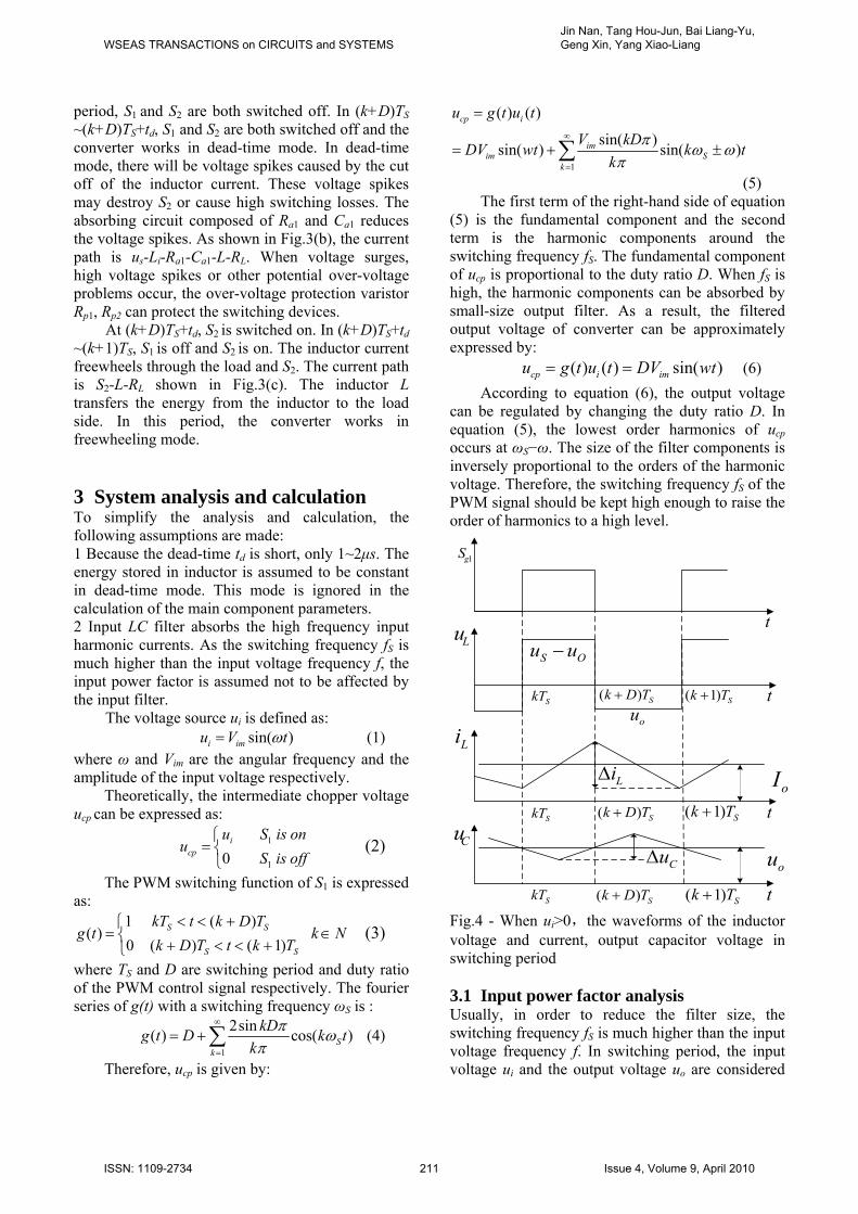
(5) is the fundamental component and the second term is the harmonic components around the switching frequency fS. The fundamental component of ucp is proportional to the duty ratio D. When fS is high, the harmonic components can be absorbed by small-size output filter. As a result, the filtered output voltage of converter can be approximately expressed by: ( ) ( ) sin( )cp i imu g t u t DV wt (6)
According to equation (6), the output voltage can be regulated by changing the duty ratio D. In equation (5), the lowest order harmonics of ucp occurs at ωS−ω. The size of the filter components is inversely proportional to the orders of the harmonic voltage. Therefore, the switching frequency fS of the PWM signal should be kept high enough to raise the order of harmonics to a high level.
t
ou
S Ou u
1gS
Li
Lu
oI
t
Cu
t
SkT
( ) Sk D T
( 1) Sk T
ou
Li
Cu
t
SkT ( ) Sk D T ( 1) Sk T
SkT
( ) Sk D T
( 1) Sk T
Fig.4 - When ui>0,the waveforms of the inductor voltage and current, output capacitor voltage in switching period 3.1 Input power factor analysis Usually, in order to reduce the filter size, the switching frequency fS is much higher than the input voltage frequency f. In switching period, the input voltage ui and the output voltage uo are considered
WSEAS TRANSACTIONS on CIRCUITS and SYSTEMSJin Nan, Tang Hou-Jun, Bai Liang-Yu, Geng Xin, Yang Xiao-Liang
ISSN: 1109-2734 211 Issue 4, Volume 9, April 2010
to be constant. When ui >0, the waveforms of inductor voltage uL and current iL are shown in fig.4.
The inductor voltage uL is : ( )
( ) ( 1)i O S S
LO S S
u u kT t k D Tu
u k D T t k T
(7)
In switching period, the average voltage of the inductor L is: ( ) (1 )L i O Ou D u u D u (8) uL can be also expressed as :
( ) LL
diu t L
dt (9)
According to equation (6), the input current ii is given by: i Li Di (10) The average voltage of ucp is:
Lcp i O
diu Du L u
dt (11)
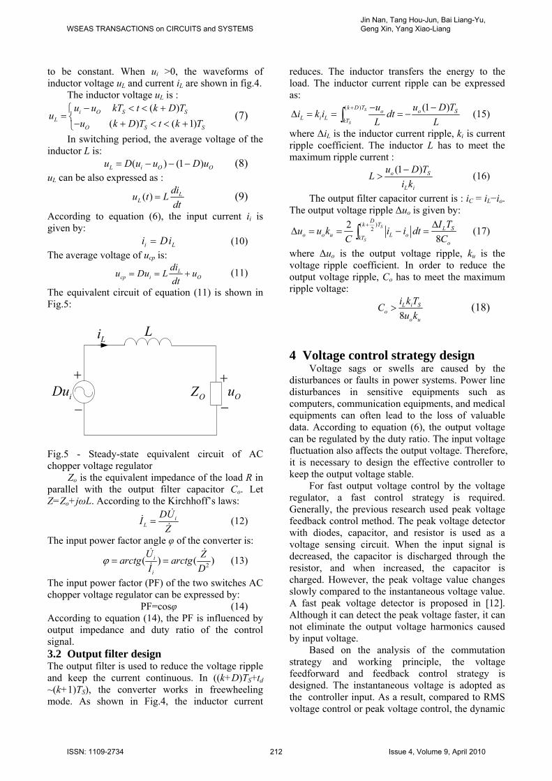
The equivalent circuit of equation (11) is shown in Fig.5:
OuiDu
Li
OZ
L
Fig.5 - Steady-state equivalent circuit of AC chopper voltage regulator
Zo is the equivalent impedance of the load R in parallel with the output filter capacitor Co. Let Z=Zo+jωL. According to the Kirchhoff’s laws:
iL
DUI
Z
(12)
The input power factor angle φ of the converter is:
2
( ) ( )i
i
U Zarctg arctg
I D
(13)
The input power factor (PF) of the two switches AC chopper voltage regulator can be expressed by: PF=cosφ (14) According to equation (14), the PF is influenced by output impedance and duty ratio of the control signal. 3.2 Output filter design The output filter is used to reduce the voltage ripple and keep the current continuous. In ((k+D)TS+td
~(k+1)TS), the converter works in freewheeling mode. As shown in Fig.4, the inductor current
reduces. The inductor transfers the energy to the load. The inductor current ripple can be expressed as:
( ) (1 )S
S
k D To o S
L i L kT
u u D Ti k i dt
L L
(15)
where ΔiL is the inductor current ripple, ki is current ripple coefficient. The inductor L has to meet the maximum ripple current :
(1 )o S
L i
u D TL
i k
(16)
The output filter capacitor current is : iC = iL−io. The output voltage ripple Δuo is given by:
( )2
2
8
S
S
Dk T
L So o u L okT
o
I Tu u k i i dt
C C
(17)
where Δuo is the output voltage ripple, ku is the voltage ripple coefficient. In order to reduce the output voltage ripple, Co has to meet the maximum ripple voltage:
8L i S
oo u
i k TC
u k (18)
4 Voltage control strategy design Voltage sags or swells are caused by the
disturbances or faults in power systems. Power line disturbances in sensitive equipments such as computers, communication equipments, and medical equipments can often lead to the loss of valuable data. According to equation (6), the output voltage can be regulated by the duty ratio. The input voltage fluctuation also affects the output voltage. Therefore, it is necessary to design the effective controller to keep the output voltage stable.
For fast output voltage control by the voltage regulator, a fast control strategy is required. Generally, the previous research used peak voltage feedback control method. The peak voltage detector with diodes, capacitor, and resistor is used as a voltage sensing circuit. When the input signal is decreased, the capacitor is discharged through the resistor, and when increased, the capacitor is charged. However, the peak voltage value changes slowly compared to the instantaneous voltage value. A fast peak voltage detector is proposed in [12]. Although it can detect the peak voltage faster, it can not eliminate the output voltage harmonics caused by input voltage.
Based on the analysis of the commutation strategy and working principle, the voltage feedforward and feedback control strategy is designed. The instantaneous voltage is adopted as the controller input. As a result, compared to RMS voltage control or peak voltage control, the dynamic
WSEAS TRANSACTIONS on CIRCUITS and SYSTEMSJin Nan, Tang Hou-Jun, Bai Liang-Yu, Geng Xin, Yang Xiao-Liang
ISSN: 1109-2734 212 Issue 4, Volume 9, April 2010

performance is improved. In addition, the feedback control part can regulate the output voltage with no steady-state error. The feedforward control part can eliminate the voltage harmonic components and suppress the voltage fluctuations effectively. The control system structure is shown in Fig.6.
u fkD
oruiu
hD
fD
D ou
oru
Fig.6 - The feedforward and feedback control system structure diagram
The steady-state input voltage is defined as: uir=uirpsin(314t) (19) The reference output voltage is: uor=uorpsin(314t) (20) uirp , uorp are the input peak-voltage and the reference output peak-voltage respectively. The steady-state duty ratio Df at the operation point is: Df =uorp/uirp (21)
Because the output voltage is proportional to the duty ratio D. The feedforward control part is designed as: (Df+Dh)ui=uor (22)
According to equation (22), the duty ratio Dh of feedforward control part is: Dh=( uor−Df ui)/ ui (23)
In previous researches, input voltage harmonics suppression has not been investigated. The proposed feedforward control uses the instantaneous value of input voltage and the reference output voltage as the controller input to regulate the duty ratio. At the operation point, the feedforward control can obtain Dh to compensate the steady-state duty ratio Df . The input voltage fluctuations can be suppressed and the harmonics can be eliminated by the feedforward control. In this way, the output voltage is stable with low harmonic distortion. This method is simple and effective. According to the circuit structure and the working principle, when ui>uor , the feedforward control can work effectively. Otherwise, the voltage drops can not be compensated.
The feedback PI control part is designed to make no steady-state error. As shown in Fig.6, the output voltage is subtracted from the reference voltage. The error voltage passes through PI
controller block and then is used to regulate the duty ratio D. The duty ratio Dfk of feedback control is given by:
( ) ( )
( )
fk p or O i
or O
D k u u k m t
dm tu u
dt
(24)
where kp, ki are proper proportional and integral gains respectively. m(t) represents the integral of the output voltage error Δu. The integral part of the designed controller makes the steady-state output voltage error zero. D is limited within the range from 0 to 1. Thus, D can be expressed as:
1 ( ) 1
0 ( ) 1
0 ( ) 0
f h fk
D t
D D D D D t
D t
(25)
The digital signal processor is used to implement the control algorithm and calculate the duty ratio in experiment. Then, the PWM control signals Sg1 and Sg2 are generated by modifying the corresponding register value in DSP directly. 5 Simulation The voltage regulator shown in Fig.1 is implemented with the following parameters: fS=40kHz, Li=100μH, Ci=1μF, C=1μF, L=1mH, Ca1= Ca2=0.1μF, Ra1= Ra2=10Ω, Ro=40Ω.
When D=0.5, the simulation results are shown in Fig.7. The input current is shown in Fig.7(b). The intermediate chopper voltage and the output voltage are shown in Fig.7(c) and Fig.7(e) respectively. The input current is nearly sinusoidal waveform. The intermediate chopper voltage ucp contains high order harmonic components. By using the output filter, the harmonic voltage is eliminated and the sinusoidal output voltage is obtained.
The snubber circuits are designed to reduce the voltage spikes in commutation process. Fig.8(a) shows the voltage across S1 without snubber circuit. There are voltage spikes with the amplitude of 20V. This will increase the power dissipation. Fig.8(b) shows the simulation results using snubber circuit. The voltage spikes are highly reduced. As a result, the designed snubber circuit can reduce the voltage spikes effectively and protect the switching devices.
WSEAS TRANSACTIONS on CIRCUITS and SYSTEMSJin Nan, Tang Hou-Jun, Bai Liang-Yu, Geng Xin, Yang Xiao-Liang
ISSN: 1109-2734 213 Issue 4, Volume 9, April 2010

-400-200
0200400
-5
0
5
-400-200
0200400
-5
0
5
0 0.02 0.04 0.06 0.08 0.1-200
0
200
Fig.7 - Simulation results of (a)input voltage ui
(b)input current ii (c)intermediate chopper voltage ucp (d)inductor current iL (e)output voltage uo
0.023 0.023 0.023 0.0231 0.0231 0.0231 0.0231-150
-100
-50
0
50
100
150
0.023 0.023 0.023 0.0231 0.0231 0.0231 0.0231-150
-100
-50
0
50
100
150
t(s)
(a)
t(s)
(b)
u(V
)u(
V)
Fig.8 - Voltage across S1 (a) without snubber circuits (b) with snubber circuits
Fig.9 shows the simulation results of the output voltage waveforms when input voltage fluctuations occur. ui and uo are input voltage and output voltage respectively. At 0.04s, input voltage increases abruptly by 15% during 5 periods. At 0.08s, input
voltage is decayed abruptly up to 15% during 3 periods. The simulation results verified that the proposed control plan can suppress the voltage fluctuations effectively.
0 0.05 0.1 0.15 0.2-400
-200
0
200
400
ui
uo
Fig.9 - Output voltage waveforms when input voltage fluctuations occur
Fig.10 shows the simulation results of the output voltage waveforms when input voltage contains harmonic components. The total harmonic distortion (THD) in input voltage is 15.54%. By using the proposed control method, the THD in output voltage is only 0.20%. The spectrum analysis is shown in Fig.6. The output voltage is a sinusoidal waveform and the voltage harmonic components are highly reduced. The simulation results confirm that the commutation process is not affected by the harmonic voltage and the designed control strategy can work effectively to eliminate the harmonic components.
0 0.01 0.02 0.03 0.04 0.05 0.06 0.07 0.08 0.09 0.1-400
-200
0
200
400
ui
uo
Fig.10 - Output voltage waveform when input voltage contains harmonic components
WSEAS TRANSACTIONS on CIRCUITS and SYSTEMSJin Nan, Tang Hou-Jun, Bai Liang-Yu, Geng Xin, Yang Xiao-Liang
ISSN: 1109-2734 214 Issue 4, Volume 9, April 2010
0
0.2
0.4
0.6
0.8
1
1.2
1 3 5 7 9 11 13 15 17 19
harmonic orders
volt
age
TH
D
input voltage
output voltage
Fig.11 - Harmonic spectrum analysis of the input and output voltage
6 Experiment
The digital signal processor (DSP) can implement with smaller size and lower cost than the general purpose microprocessor. Moreover, compared to the microcontroller, DSP has higher processing speed and more powerful ability in executing complex control algorithm. In experiment, the overall system is divided into two parts: the controller and the power circuit. The controller part includes the DSP running the proposed control algorithms. The feedforward and feedback control algorithm of the proposed voltage regulator is implemented using a DSPIC30f4011. Switching period and duty ratio calculation are implemented in software. The PWM pulses are generated by the PWM module in the DSP. Voltage signals are measured by using the analog digital converter (ADC) module in DSP. The implementation of the voltage controllers and PWM pulse generation is performed in every switching period. The bilateral switch consists of the IGBT and the fast recovery diode rectifier. 10A/600V IGBT and 10A/600V fast recovery diodes are selected as the switching devices. These switches are operated at a fixed switching frequency 40kHz and a dead time of 1 us.
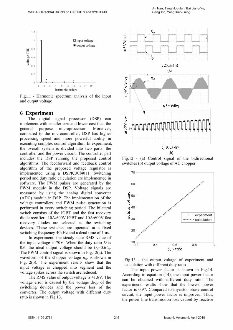
In experiment, the steady-state RMS value of the input voltage is 70V. When the duty ratio D is 0.6, the ideal output voltage should be Uo=0.6Ui. The PWM control signal is shown in Fig.12(a). The waveform of the chopper voltage ucp is shown in Fig.12(b). The experiment results show that the input voltage is chopped into segment and the voltage spikes across the switch are reduced.
The RMS value of output voltage is 41.6V. The voltage error is caused by the voltage drop of the switching devices and the power loss of the converter. The output voltage with different duty ratio is shown in Fig.13.
Fig.12 - (a) Control signal of the bidirectional switches (b) output voltage of AC chopper
0.2 0.4 0.6 0.8 110
20
30
40
50
60
70
experiment
calculation
Fig.13 - the output voltage of experiment and calculation with different duty ratio
The input power factor is shown in Fig.14. According to equation (14), the input power factor can be obtained with different duty ratio. The experiment results show that the lowest power factor is 0.97. Compared to thyristor phase control circuit, the input power factor is improved. Thus, the power line transmission loss caused by reactive
WSEAS TRANSACTIONS on CIRCUITS and SYSTEMSJin Nan, Tang Hou-Jun, Bai Liang-Yu, Geng Xin, Yang Xiao-Liang
ISSN: 1109-2734 215 Issue 4, Volume 9, April 2010
power can be reduced. The power transfer efficiency with different
duty ratio is shown in Fig.15. In this experiment, the highest power transfer efficiency can be achieved at 96.8%. The experiment results verify that the proposed voltage regulator has high power factor and high efficiency.
0.2 0.4 0.6 0.8 10.9
0.92
0.94
0.96
0.98
1
calculation
experiment
Fig.14 - input power factor characteristics of experiment and calculation with different duty ratio
0.2 0.3 0.4 0.5 0.6 0.7 0.8 0.9
0.75
0.8
0.85
0.9
0.95
1
R=40R=100
Fig.15 - power transfer efficiency characteristics When input voltage fluctuations occur, the
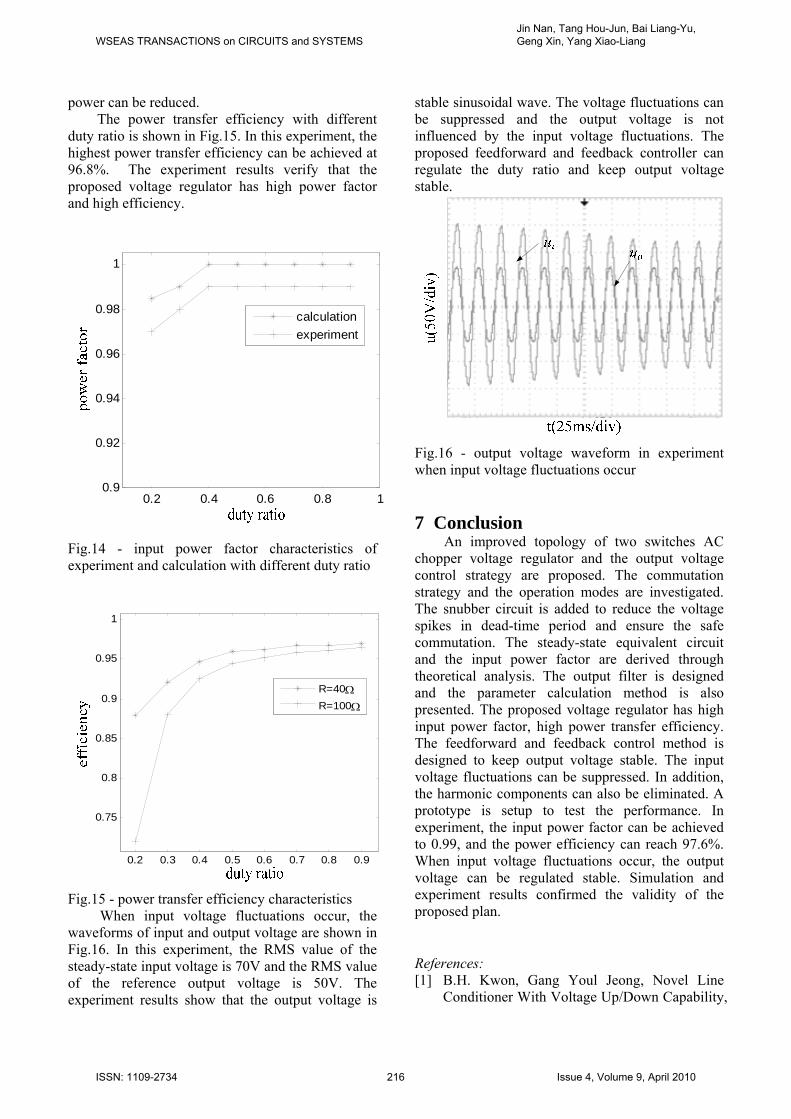
waveforms of input and output voltage are shown in Fig.16. In this experiment, the RMS value of the steady-state input voltage is 70V and the RMS value of the reference output voltage is 50V. The experiment results show that the output voltage is
stable sinusoidal wave. The voltage fluctuations can be suppressed and the output voltage is not influenced by the input voltage fluctuations. The proposed feedforward and feedback controller can regulate the duty ratio and keep output voltage stable.
Fig.16 - output voltage waveform in experiment when input voltage fluctuations occur
7 Conclusion An improved topology of two switches AC
chopper voltage regulator and the output voltage control strategy are proposed. The commutation strategy and the operation modes are investigated. The snubber circuit is added to reduce the voltage spikes in dead-time period and ensure the safe commutation. The steady-state equivalent circuit and the input power factor are derived through theoretical analysis. The output filter is designed and the parameter calculation method is also presented. The proposed voltage regulator has high input power factor, high power transfer efficiency. The feedforward and feedback control method is designed to keep output voltage stable. The input voltage fluctuations can be suppressed. In addition, the harmonic components can also be eliminated. A prototype is setup to test the performance. In experiment, the input power factor can be achieved to 0.99, and the power efficiency can reach 97.6%. When input voltage fluctuations occur, the output voltage can be regulated stable. Simulation and experiment results confirmed the validity of the proposed plan. References: [1] B.H. Kwon, Gang Youl Jeong, Novel Line
Conditioner With Voltage Up/Down Capability,
WSEAS TRANSACTIONS on CIRCUITS and SYSTEMSJin Nan, Tang Hou-Jun, Bai Liang-Yu, Geng Xin, Yang Xiao-Liang
ISSN: 1109-2734 216 Issue 4, Volume 9, April 2010

IEEE Transactions On Industrial Electronics, Vol.49, No.5, pp.1110-1119, 2002
[2] S.M. Hietpas, M. Naden, Automatic voltage regulator using an AC voltage-voltage converter, IEEE Transaction on Industry Application, Vol.36, No.1, pp.33-38, 2000
[3] Veszpremi K, Hunyar M., New application fields of the PWM IGBT AC chopper, Eighth International Conference of Power Electronics and Variable Speed Drives, pp. 46-51, 2000
[4] Bodur H., Bakan A.F., Sarul M.H., Universal motor speed control with current controlled PWM AC chopper by using a microcontroller, Proceedings of IEEE International Conference on Industrial Technology,Vol.2, pp. 394-398, 2000
[5] Sundareswaran K., Rajasekar N., Sreedevi V.T., Performance comparison of capacitor-run induction motors supplied from AC voltage regulator and SPWM AC chopper, IEEE Transactions on Industrial Electronics, Vol.53, pp.990-993, 2006
[6] Shinichiro Fujikura, Akiteru Ueda, and Akihiro Torii, Analysis of a Three-Phase Buck-Boost AC Chopper Controlled in Two Phases, Power Conversion Conference, pp.824-830, 2007
[7] Geraldo C. R. Sincero and Arnaldo José Perin, High Pressure Sodium Lamp High Power Factor Electronic Ballasts Using AC–AC Converters, IEEE Transactions On Power Electronics, 2007,Vol. 22, No. 3: 804-814
[8] Balci M.E., Hocaoglu M.H. Effects of Source Voltage Harmonic Distortion on Power Factor Compensation in Triac Controlled AC Chopper Circuits, International conference on PEDS, Vol. 2, pp. 1199–1204, Nov., 2005
[9] Nabil A. Ahmed, Kenji Amei, and Masaaki Sakui, A New Configuration of Single-Phase Symmetrical PWM AC Chopper Voltage Controller, IEEE Transactions On Industrial Electronics, Vol. 46, No. 5, pp.942-952, 1999
[10] N.A. Ahmed, Kenji Amei and Masaaki Sakui, Improved Circuit of AC Choppers for Single-Phase System, Proceedings of the IEEE Conference PCCON, Vol.2, pp. 907-912, 1997
[11] Takayuki Shinyama, Makoto Kawai, Akihiro Torii, Akiteru Ueda, Characteristic of an AC Chopper Circuit with LC Filters in the Input and Output Side, Electrical Engineering in Japan, Vol.155, No.2, pp.45-52, 2006
[12] B.H. Kwon, J.H.Youm, J.H. Choi, Automatic voltage regulator with fast dynamic speed, IEE Proceedings of Electrical Power Application, Vol.146, No.2, pp.201-207, 1999
[13] J.H. Kim, B.D. Min, and B.H. Kwon, A PWM Buck–Boost AC Chopper Solving the Commutation Problem, IEEE Transactions On Industrial Electronics, Vol. 45, No. 5, pp.832-835, 1998
[14] Shinyama T, Ueda A, and Torii A, AC chopper using four switches, Proceedings of Power Conversion conference, pp.1056-1060, 2002
[15] S. Polmai, E. Sugprajun, Experiment On Instantaneous Value Voltage Control of a Single Phase AC Chopper, Proceedings of the IEEE Conference PCCON 07, pp.77-82 , 2007
WSEAS TRANSACTIONS on CIRCUITS and SYSTEMSJin Nan, Tang Hou-Jun, Bai Liang-Yu, Geng Xin, Yang Xiao-Liang
ISSN: 1109-2734 217 Issue 4, Volume 9, April 2010