analysis and design of high gain, and low power cmos ... · analysis and design of high gain, and...
TRANSCRIPT
Amirkabir University of Technology
(Tehran Polytechnic)
Vol. 45, No. 1, spring 2013, pp. 35- 50
Amirkabir International Journal of Science& Research
(Electrical & Electronics Engineering)
AIJ-EEE))
٭Corresponding Author, Email: [email protected]
Vol. 45, No. 1, spring 2013 35
Analysis and Design of High Gain, and Low Power
CMOS Distributed Amplifier Utilizing a Novel Gain-cell
based on Combining Inductively Peaking and Regulated
Cascode Concepts
Z. Baharvand1
, A. Hakimi2
1- MSc Student, Department of Electrical and Computer Engineering, Graduate University of Advanced Technology, Kerman, Iran.
2- Assistant Professor, Department of Electrical Engineering, Shahid Bahonar University of Kerman, Kerman, Iran.
ABSTRACT
In this study an ultra-broad band, low-power, and high-gain CMOS Distributed Amplifier (CMOS-DA)
utilizing a new gain-cell based on the inductively peaking cascaded structure is presented. It is created by
cascading of inductively coupled common-source (CS) stage and Regulated Cascode Configuration (RGC).
The proposed three-stage DA is simulated in 0.13 μm CMOS process. It achieves flat and high of 26.5 ±
0.4 dB over the frequencies range from DC up to 13 GHz 3-dB bandwidth, and it dissipates only 9.95 mW.
The IIP3 is simulated and achieved -10 dBm at 6 GHz. Also, simulated input referred 1-dB compression
point at 6 GHz achieves the value of -20 dBm. Both input and output matches are better than -11 dB. To
obtain the low power and high gain requirements, the advantages of the bulk terminal are exploited in the
proposed CMOS-DA. It adopts the method of forward body biasing in output MOS transistor to achieve
higher transconductance and lower power consumption. Additionally, the Monte Carlo (MC) simulation is
performed to take into account the risks associated with various input parameters which they receive little or
no consideration in simulating of designs utilizing ideal components. MC simulation predicts an estimate of
the good accuracy performance of the proposed design under various conditions.
KEYWORDS
CMOS Distributed Amplifier, High-Gain, Ultra-broad Band, Low Power, Regulated Cascode
Configuration.
Amirkabir International Journal of Science& Research
(Electrical & Electronics Engineering)
(AIJ-EEE)
Vol. 45, No. 1, spring 2013 36
1- INTRODUCTION
The low-cost, easy integration and the latest
performance developments driven by forceful scaling of nanometer complementary-metal-oxide-semiconductor
(CMOS) technology have made it feasible to realize the
radio frequency (RF) systems [1]. The high-rate
requirement for broadband communication systems
demands the wideband amplifiers as essential building
blocks. Distributed amplifier (DA) is appeared as one of
the most prevalently candidates for broadband
amplification applications. The reason of choosing DAs,
as a prime solution for extremely wideband amplification
applications is their high gain-bandwidth product and
excellent linearity in nature [1, 2].
The existing trade-offs in CMOS-DA designing
introduce significant design considerations with regards
to gain, bandwidth, and power consumption. The
conventional CMOS-DAs have the additive gain
mechanism, and their gain is not significantly high.
Besides, the low gain drawback in CMOS process is
further critical as a result of the low transconductance and
high substrate loss in a silicon-based process [3]. In
addition, one of the main issues of DAs design is their
large DC power dissipation. The high power dissipation
of the DAs critically restricts their usage in wireless
portable devices [4]. In general, there are two choices in
implementing the high gain and broad bandwidth CMOS-
DAs. One is based on the cascaded gain-cells topology,
and the other is two-dimensional DAs which are
discussed as follows:
Ref. [4] introduces a 0.18 μm CMOS-DA utilizing
cascade of inductively coupled common source (CS)
gain-cells for gain improvement at high frequencies. The
DA is attained extraordinary flat and high gain of 10 ±
1.5 dB at low-gain (LG) mode and 16 ± 1.5 dB at high-
gain (HG) mode. But, the corresponding of 19.6 mW
at LG mode and 100 mW at HG mode are not desire. Ref.
[5] demonstrates a 0.13 μm two-stage CMOS-DA with
cascaded gain-cell, which comprises two enhanced
CMOS inverters. This work achieved high power gain of
11.4 ± 1.4 dB at LG mode and 17.1 ± 1.5 dB at HG
mode, respectively. The design at HG mode consumes
of 30 mW isn’t decent. The design of Ref. [6]
illustrates a CMOS-DA in 0.13 μm by utilizing cascaded
gain-cell that constitutes by an inductively parallel-
peaking cascode stage with a low-Q RLC load and an
inductively series peaking CS stage. The flat and high
gain of 11.03 ± 0.98 dB at the LG mode and 20.47 ± 0.72
dB at the HG mode are achieved. However, this DA
achieves an excellent average noise figure (NF) of 4.25
dB at LG mode and 3.29 dB at HG mode, but the
corresponding of 37.8 mW is at the medium range
and hasn’t very low value. Finally, in Ref. [7] with
modified cascade gain-cell is demonstrated that it is
possible to achieve a high gain and low power
consumption, concurrently. However, the corresponding
average NF of 6.6 dB at LG mode and 6.5 dB at HG
mode aren’t satisfactory. As a general result, the
mentioned designs are based on the cascade gain-cell
topology which can’t provide enough gain and bandwidth
at very low power consumption or low power dissipation
at the high gain levels.
Two-dimensional DAs have been suggested to take the
benefits of multiplicative gain mechanism, such as cascaded single-stage distributed amplifiers (CSSDAs)
[3], cascaded multi-stage distributed amplifier (CMSDA)
[2, 8], and matrix DA [8], composition of the
conventional DA and the cascaded single stage DA [3],
DA with cascaded gain stages [9] and DA with internal
feedback [10].
Even though the two-dimensional DAs have potential
of higher gain-bandwidth performance than other DA
configurations, their high power consumption and big
chip-area aren’t satisfactory. These drawbacks of two-
dimensional DAs seriously restrict their usage in wireless
portable devices. As it can be seen, in reported various
types of DAs, gain, bandwidth, and power dissipation are
significant criteria in the design of DAs.
Biasing the active devices of DA at a very low
overdrive voltage improves the power consumption at the
expense of insufficient gain. Also, raising the gain of
CMOS-DAs generally comes at the deep trade-off in
bandwidth. Therefore, as a research motivation one can
try to optimize the performance of CMOS-DA regarding
the gain, bandwidth, power dissipation and noise figure.
Here, a novel gain-cell is presented to pick the optimal
performance and topology which it meets these targets.
This paper discusses the design of a high gain, ultra-broad
bandwidth, and low power CMOS-DA.
To guarantee the expected behaviour of the proposed
CMOS-DA it is necessary to determine how it will
operate in every possible situation, which is yielded by
MC simulation. MC simulation is performed to consider
the effect of parameters variation including fluctuations
in MOS parameters which are unavoidable in practice
also, supply voltage variations, and tolerance effects of
passive components to understand the impact of risk and
uncertainty in computing the results. Following this
introduction, Section 2 elaborates upon the circuit design
of the proposed CMOS-DA. Simulation and
Amirkabir International Journal of Science& Research
(Electrical & Electronics Engineering)
(AIJ-EEE)
Analysis and Design of High Gain, and Low Power CMOS Distributed
Amplifier Utilizing a Novel Gain-cell based on Combining Inductively Peaking
and Regulated Cascode Concepts
Vol. 45, No. 1, spring 2013 37
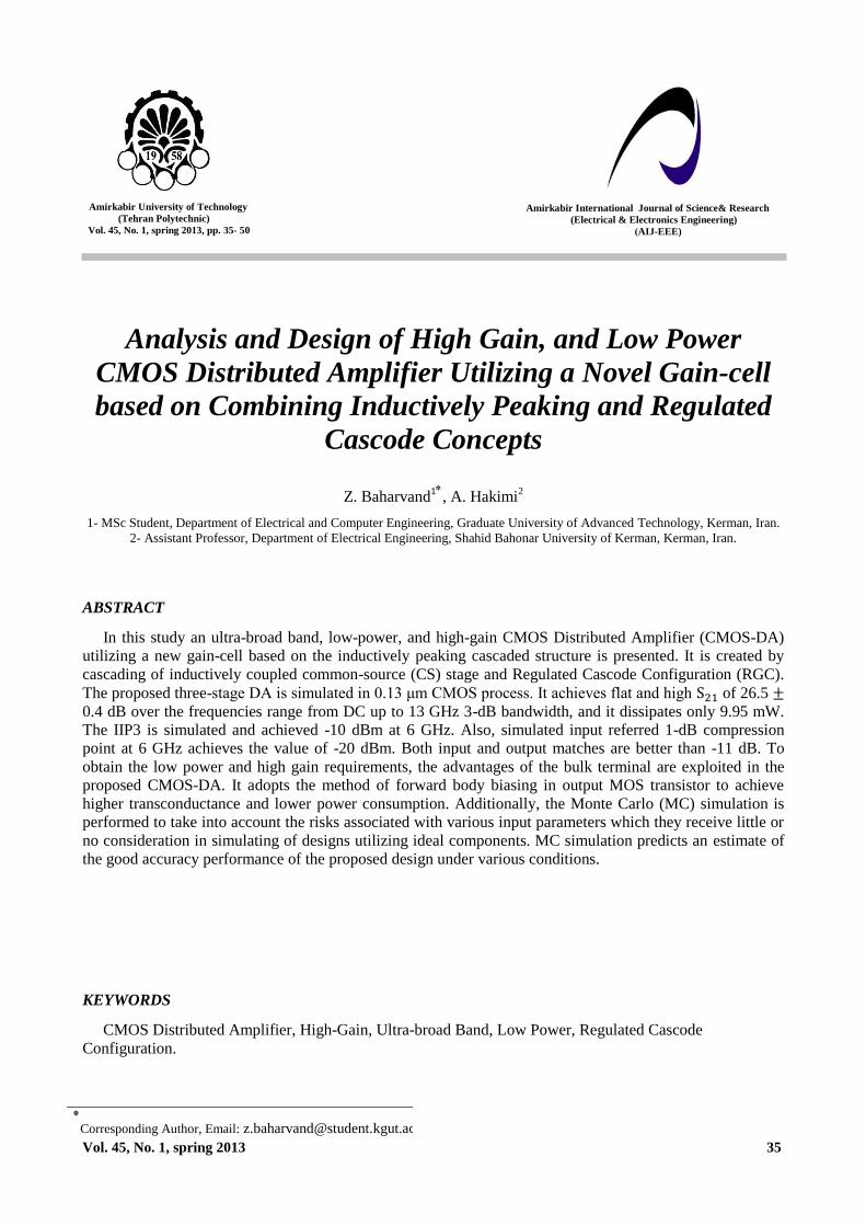
Figure 1: Circuit schematics of the conventional DA
comparative results are discussed in Section 3. Finally,
Section 4 presents the conclusion of the work.
2- BASIC PRINCIPLE OF PROPOSED DA
The main idea behind of a DA relies on the operation
of a pair synthesized transmission line (TL). TLs
constitutes by series on-chip inductors in conjunction
with the shunt parasitic capacitances from active devices,
which are the input gate-line and the output drain-line.
The input and output TLs are terminated in their
characteristic impedance at the end of the lines. This is
because of the reflections won’t occur. The parasitic
capacitances of the active devices which are the major
reason of bandwidth restriction absorb into TLs, and the
extensive bandwidth response is attained. The active
devices are coupled into the drain line through the
transconductance of them. The input signal is sent at the
input-gate line while it travels down on the gate line, each
of the active devices is triggered by the propagating input
signal.
Finally, the traveling input signal is absorbed at the
termination end of the gate line. The active devices feed a
current into the output-drain line. Fig. 1 shows the
simplified schematic of an original DA with CS stages as
active devices [11-13].
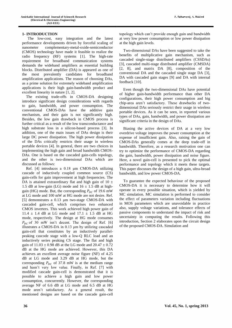
Fig. 2 shows the schematic of the proposed CMOS-DA
based on the new gain-cell note that, biasing not shown
for simplicity. The proposed gain-cell construction
illustrates that it is practicable to achieve flat and high
gain, and low-power dissipation for a CMOS-DA,
concurrently. The new gain-cell uses the inductively
coupled cascaded structure, which is shaped by a cascade
of inductively coupled CS stage and a Regulated Cascode
Configuration (RGC).
Figure 2: Schematic of three-stage CMOS-DA based on the proposed cascaded gain cell
Amirkabir International Journal of Science& Research
(Electrical & Electronics Engineering)
(AIJ-EEE)
Z. Baharvand
Vol. 45, No. 1, spring 2013 38
In the next sub-sections the effects of inductively
coupled cascaded structure and the effect of the RGC,
define in details. They aim to realize the balanced trade-
off between critical challenges in high gain and broad
bandwidth DAs designing. For stability consideration, the
gates of (i = 2, 3) devices at each gain-cell are
bypassed through (i= 1, 2) resistors in series with DC-
BLOCK capacitors. Note that, this section of the circuit is
omitted in the Fig. 2 for simplicity.
A- INDUCTIVELY COUPLED CASCADED
STRUCTURE
The cascaded gain-cells increase the amplifier’s gain
while operating in low voltage and low power conditions.
However, the lack of an ultra-broad band response arises
from imposing multiple poles is main issue that they face
with it. Inductively coupled cascaded structure that
shaped based on inductive peaking concept has been
addressed in Ref. [4] to circumvent the influence of the
traditional cascaded gain-cell’s restricted bandwidth. It
creates a zero that can be used to cancel the effect of
dominate pole and to increase the amplifier’s bandwidth
to farther pole. It is a helpful approach to alleviate the
effects of imposing multiple poles that associated with the
inter-stage parasitic capacitances due to increase cascaded
stages. This method is employed in this design that makes
it possible to meet the high gain performance of the
proposed cascaded gain-cell, without sacrificing the
bandwidth.
Moreover, to avoid of limiting the total bandwidth by
the pole associated with the RGC cell’s internal node,
inductive peaking embedded in the source of
device in each gain-cell. Another benefit of is the
transconductance improvement. As a result, more gain
can be achieved without make larger the power
dissipation. This effect arises from the fact that
employing enables us to raise the transistor aspect ratio
and to earn the objective transconductance with lower
power dissipation while the similar bandwidth is obtained
at the same time [9, 14, 15].
The inductive peaking inductors including and
not only extends the bandwidth, but also substantially
maintain pass-band gain flatness. This sub-section
investigated the effects of inductively coupled cascaded
structure on extending bandwidth. The next sub-section
elaborates the effect of RGC upon increasing the output
impedance as a result increasing the gain. It shows how
large effect is obtained by utilizing of RGC.
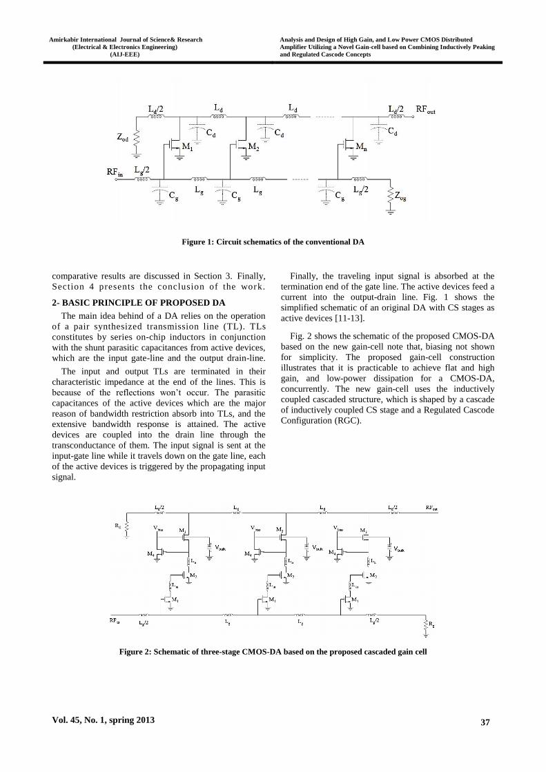
B- REGULATED CASCODE CONFIGURATION
In order to avoid the utilizing of stacked structure that
is unsuited to boost the gain in low supply voltage
applications the RGC can be used [16, 17]. RGC not only
substantially increases the output impedance and the gain,
but also remove the voltage headroom’s obstacle of
conventional cascode architecture. To highlight the more
favorable aspects of the RGC than conventional cascode
cell, these structures are compared against each other as
follows:
Fig. 3 illustrates the conventional cascode
configuration versus RGC structure. The output
impedance of conventional cascode cell (see Fig. 3 (a))
can be calculated as (1), that device plays
degeneration resistor’s role:
(a) (b)
Figure 3: Schematic of a) conventional cascode cell b) regulated cascode configuration cell
Amirkabir International Journal of Science& Research
(Electrical & Electronics Engineering)
(AIJ-EEE)
Analysis and Design of High Gain, and Low Power CMOS Distributed
Amplifier Utilizing a Novel Gain-cell based on Combining Inductively Peaking
and Regulated Cascode Concepts
Vol. 45, No. 1, spring 2013 39
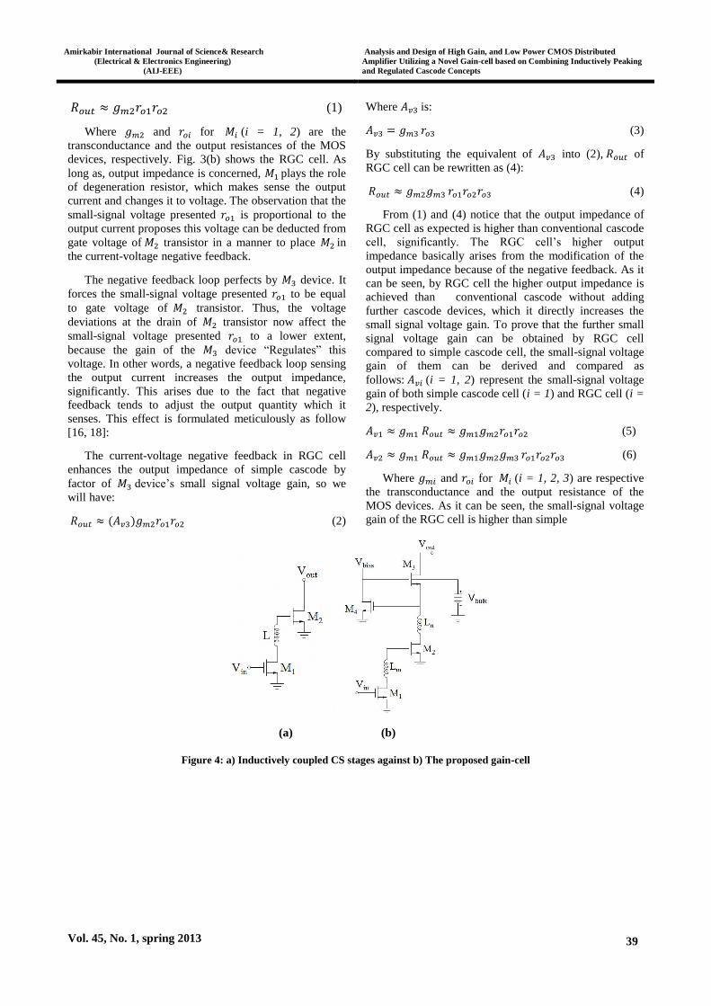
(1)
Where and for (i = 1, 2) are the
transconductance and the output resistances of the MOS
devices, respectively. Fig. 3(b) shows the RGC cell. As
long as, output impedance is concerned, plays the role
of degeneration resistor, which makes sense the output
current and changes it to voltage. The observation that the
small-signal voltage presented is proportional to the
output current proposes this voltage can be deducted from
gate voltage of transistor in a manner to place in
the current-voltage negative feedback.
The negative feedback loop perfects by device. It
forces the small-signal voltage presented to be equal
to gate voltage of transistor. Thus, the voltage
deviations at the drain of transistor now affect the
small-signal voltage presented to a lower extent,
because the gain of the device “Regulates” this
voltage. In other words, a negative feedback loop sensing
the output current increases the output impedance,
significantly. This arises due to the fact that negative
feedback tends to adjust the output quantity which it
senses. This effect is formulated meticulously as follow
[16, 18]:
The current-voltage negative feedback in RGC cell
enhances the output impedance of simple cascode by
factor of device’s small signal voltage gain, so we
will have:
(2)
Where is:
(3)
By substituting the equivalent of into (2), of
RGC cell can be rewritten as (4):
(4)
From (1) and (4) notice that the output impedance of
RGC cell as expected is higher than conventional cascode
cell, significantly. The RGC cell’s higher output
impedance basically arises from the modification of the
output impedance because of the negative feedback. As it
can be seen, by RGC cell the higher output impedance is
achieved than conventional cascode without adding
further cascode devices, which it directly increases the
small signal voltage gain. To prove that the further small
signal voltage gain can be obtained by RGC cell
compared to simple cascode cell, the small-signal voltage
gain of them can be derived and compared as
follows: (i = 1, 2) represent the small-signal voltage
gain of both simple cascode cell (i = 1) and RGC cell (i =
2), respectively.
(5)
(6)
Where and for (i = 1, 2, 3) are respective
the transconductance and the output resistance of the
MOS devices. As it can be seen, the small-signal voltage
gain of the RGC cell is higher than simple
(a) (b)
Figure 4: a) Inductively coupled CS stages against b) The proposed gain-cell

Amirkabir International Journal of Science& Research
(Electrical & Electronics Engineering)
(AIJ-EEE)
Z. Baharvand
Vol. 45, No. 1, spring 2013 40
cascode cell, significantly. It is similar to the gain of
triple cascode amplifier while reducing voltage
headroom’s drawback that unavoidable in the cascode
circuits is removed.
To show how large effect is obtained in this work by
utilizing of combined inductively peaking and RGC
concepts, this work is compared with Ref. [4] that utilizes
cascade of inductively coupled CS gain-cells. Fig. 4
illustrates the gain-cell of Ref. [4] against the proposed
gain-cell. The total voltage gain , of both
inductively coupled CS gain-cells (i=1) and the proposed
gain-cell (i=2) to be equal to the product of voltage gain
of both stages that shaped each of them, it can be
calculated according to (7):
(7)
The equivalent’s total voltage gain of inductively
coupled CS gain-cells is given as (8):
(8)
Also, the equivalent’s total voltage gain of the
proposed gain-cell is written as follows:
(9)
As it can be seen, the equivalent’s total voltage gain
of the proposed gain-cell is higher than inductively
coupled CS gain-cells, substantially. So it can be said
that, large effect of the new gain- cell than previous
viable cascaded gain-cells in high gain DAs designing
like the gain-cell of Ref. [4] which is the nearest work to
the proposed gain-cell is obtained as a result of RGC
cell’s higher gain. As a consequence, combining
inductive peaking and RGC concepts resulted in design of
a high gain and broadband DA based on a
new gain-cell. Note that, the parasitic capacitances in
these theoretical analyses are ignored for simplicity. They
take into account in high frequency transconductance
analysis of the proposed CMOS-DA which
is necessary factor to calculate the CMOS-DA’s power
gain.
2- 1- EXPLOITING THE ADVANTAGES OF
THE BULK TERMINAL
Even though, the MOS transistor has four terminals,
but it is usually utilized as a three terminals device. In
view of the fact that its bulk and source terminals are tied
to each other and both are shorted to a supply voltage.
Since the gain of a MOS amplifier depends on its
transconductance , one can enhance the
transconductance as a result the gain of the amplifier
using the bulk terminal of transistor. Another bulk
terminal’s feature is to reduce the threshold voltage to overcome the voltage’s limitation in low power
applications [19, 20]. These benefits more highlight by
follow descriptions:
2- 1- 1- Gain increasing by optimizing bulk-to-source
voltage
A MOS transistor as a four terminals device has two
dependent current sources which cause a related current
with and voltages in drain terminal of
transistor. Note that, and are appeared voltages
on the gate-to-source and bulk-to-source capacitors. By
taking derivatives of to and , the bulk
transconductance and the total transconductance
relation of a MOS transistor can be extracted according to
(10), (11):
√| | (10)
(11)
As it can be seen, from equation (10) value
depended on bulk-to-source voltage. Optimizing the bulk-
to-source voltage can increase the value, results in it
can increase the . As mentioned above, since the
gain of a MOS amplifier is relative to its
transconductance, hence from equation (11) it can be said
that, the forward body biasing increases the value, as
a result increases the total transconductance that it
directly increases the gain of a MOS amplifier.
Moreover, if the bulk effect of the output MOS of
RGC cell is considered, RGC’s output impedance and
small signal voltage gain can be further improved. The
output impedance also, the small signal voltage gain of
RGC cell with bulk effect rewritten as (12), (13) that it confirms they are higher than their counterpart in the both
of simple cascode and traditional RGC.
(12)
(13)
The forward body biasing has been used in output
MOS device of the proposed gain-cell for achieving more
output impedance result in further gain. Also, it enhances
the DA’s power gain as a result of enhancing the total
high frequency small signal transconductance. This claim
validates by total high frequency small signal
transconductance analysis of the proposed gain-cell that it
will present in sub-section 2.4.
2- 1- 2- POWER CONSUMPTION REDUCING
BY OPTIMIZING BULK –TO-SOURCE VOLTAGE
As previously mentioned, one of the possible methods
to overcome the voltage bounds is to set by . It is
possible to decline the through either technology
scaling or circuital technique [19]. The circuital approach
counts on taking the profit of the MOS body-effect that is
to rely on forward body biasing to reduce the value
of . Equation (14) shows the dependency of to

Amirkabir International Journal of Science& Research
(Electrical & Electronics Engineering)
(AIJ-EEE)
Analysis and Design of High Gain, and Low Power CMOS Distributed
Amplifier Utilizing a Novel Gain-cell based on Combining Inductively Peaking
and Regulated Cascode Concepts
Vol. 45, No. 1, spring 2013 41
(√| | √| |) (14)
Where refers to the threshold voltage of MOS at
zero substrate voltage, is the bulk Fermi potential,
represents a constant describing the substrate bias
influence, illustrates the fixed gate-to-source voltage.
As it can be seen, the effect of a voltage difference
between the bulk and source terminals directly influence
the amplitude. By analyzing (14), it can be said that
the changes when changing .
In the other words, by applying a positive the
magnitude of the can be decreased. The simulation
result of reducing of by moderating the through
forward body biasing is shown in Fig. 5.
Decreasing of has been validated by simulation
result, as expected. In the standard 0.13 μm CMOS
process, the value of for a typical BSIM3 NMOS
transistor model is about 0.43 V. As it can be seen from
Fig. 5 (b), by applying a positive the magnitude of the
can be reduced. In this design the value of for
output MOS device reduces from 0.43-V to 0.23-V as a
result of employing of forward body biasing method. The
optimum value of forward body bias voltage for
simulation is about 1 V.
This means that, a lower gate voltage is now
demanded which able to turn the MOS on. Therefore, a
lower drain voltage can be utilized for MOS device that
operates in strong inversion region. This effect is
employed in output MOS device of the proposed gain-cell
to reduce the drain voltage of it. This voltage is the same
voltage which directly uses in calculating DC power
dissipation of DAs. The total DC power dissipation of the
DA is as follows:
(15)
Where represents the drain current through one
stage’s output. N refers to the number of DA’s stages.
is the bias voltage of DA’s drain line and the drain
voltage of the output MOS that is reduced by utilizing of
forward body biasing to achieve lower DC power
consumption. In this design, the value of for
simulation is about 0.87 V.
(a) (b)
Figure 5: a) MOS transistor as a four terminals device, and b) The modification of by moderating the bulk-source
voltage through forward body biasing
Appling the MOS body-effect in conjunction with
cascaded topology that operates at low voltage and low
power conditions enhance the gain, considerably while
the power consumption keeps as low as possible over the
entire interest band.
2- 2- THE HIGH FREQUENCY
TRANSCONDUCTANCE ANALYSIS OF THE
PROPOSED GAIN CELL
As mentioned earlier, the power gain of the CMOS-
DA depends on the total transconductance of its gain-cell.
Therefore, the total high frequency small-signal
transconductance of the proposed gain-cell by
taking into account parasitic capacitances must be carried
on for calculating the power gain of DA. The next sub-
section is provided this significant. Fig. 6 (a) and (b)
display the circuit schematic and the high frequency
small-signal equivalent circuit of the proposed gain-cell,
which are utilized to calculate the
corresponding
Calculating of is necessary because
according to DA’s power gain formula with assuming
lossless TLs that is provided in (16), it is only unknown
factor to calculate the DA’s power gain [13].
| |
| | (16)
Where represents the gain-cell’s
transconductance of the DAs which shape based on new
gain-cells, is the TL’s characteristic impedance (
), and N refers to the number of DA’s stages [13].
(i = 1, 2, 3, 4) that are shown by dashed
capacitors in Fig. 6 (a), represent the parasitic gate-to-

Amirkabir International Journal of Science& Research
(Electrical & Electronics Engineering)
(AIJ-EEE)
Z. Baharvand
Vol. 45, No. 1, spring 2013 42
source and drain-to-bulk capacitances of the MOS
devices in the proposed gain-cell. In this analysis,
suppose that parasitic gate-to-drain capacitance from
each NMOS device combines with its and by
employing the Miller effect to shape and .
Also, and (i = 1, 2, 3, 4) are the
transconductances and the output resistances of the
NMOS transistors, respectively. Note that, (i = 1, 2)
and (i = m, n) refer to the resistors and inductors that
are utilized in each gain-cell. As discussed earlier, the
(i = 1, 2) are belong the biasing circuit which not
shown in Fig. 2 for simplicity.
Typically, (i = 1, 2, 3, 4) are relatively large hence,
they can be disregarded. The total high frequency small
signal transconductance of the new gain-cell can be
derived as follows:
(17)
(a)
(b)
Figure 6: a) The circuit schematic, and b) The high frequency small-signal equivalent circuit of the proposed gain-cell
The gate voltage of to ground is equal to
multiplied by small signal voltage gain of
device named (– ). Note that, device realized the
negative feedback loop. In Fig. 6 (b), device is shown
by a block with gain of – also, its small-signal
equivalent circuit placed in a dashed box for simplicity of
high frequency analysis. Thus, the gate-to-source voltage
of can be given as follows:
(18)
With a KCL at the output node of Fig. 6 (b) it can be
achieved that:
(19)

Amirkabir International Journal of Science& Research
(Electrical & Electronics Engineering)
(AIJ-EEE)
Analysis and Design of High Gain, and Low Power CMOS Distributed
Amplifier Utilizing a Novel Gain-cell based on Combining Inductively Peaking
and Regulated Cascode Concepts
Vol. 45, No. 1, spring 2013 43
As a result:
(20)
By writing a KVL in the path of and it can be
given that:
(21)
From KCL at the , and nodes we have:
(22)
(
)
(23)
As a consequence, the can be rewritten as
(24):
(
)
(24)
Where shows the small signal voltage gain
of device. The factor is calculated according to (25),
from its small-signal equivalent circuit that it
demonstrated in the dashed box in Fig. 6 (b):
(25)
Note that, there are two zeroes in the expression
of that associated with peaking inductive
coupled cascaded concept (see in Fig. 6 (a) and 6 (b)).
Therefore, these zeroes can be utilized to increase the
bandwidth of the amplifier by canceling the effect of
dominate poles. Moreover as discussed earlier, the
expression of in relation,
validates increasing the power gain of the proposed
CMOS-DA by utilizing of forward body biasing in output
MOS device.
2- 3- VELOCITY MATCHING OF THE
PROPOSED CMOS-DA
The phase velocity of a signal traveling upon a TL can
be written as (26) [13]:
√
√
√ (26)
Combining (26) with the expression of the lossless
TL’s characteristic impedance, which is given according
to (27) [13]:
√
√
√
(27)
Allows one to achieve expressions for the phase
velocities upon both the gate, and drain lines as follows
[13]:
(28)
(29)
Observing (28), (29) show that the larger series
inductance of the gate line introduces additional phase
delay, thus making it necessary to increase the delay
incurred in the drain line by an equal amount. In practice
case, it can be implemented by increasing the length of
the drain line , sufficiently to satisfy the below
relationship:
(30)
Where , represent the equivalent series inductors
of the gate and drain lines, and , are the length of
segment lines at gate and drain, respectively.
2- 4- BROADBAND INPUT IMPEDANCE OF THE
PROPOSED CMOS-DA
The circuit schematic of a typical three-stages DA and
its input equivalent circuit shown in Fig. 7 (a) and 7 (b).
They are utilized to describe the input impedance
matching. Note that, circuit biasing and drain TL are
removed for simplicity. As discussed earlier, for
simplicity of high frequency analysis suppose that
parasitic gate-to-drain capacitance from each NMOS
device combines with its and by employing the
Miller effect, to shape and . Following this
description, and (i = 1, 2, 3) are the inductance
of the gate TL and the equivalent parasitic capacitance at
the input node of the each gain-cell also, represents
the gate-termination resistor, respectively. This idea allows to decompose the proposed DA’s circuit into
separate loaded TLs for the gate and drain terminals for impedance matching calculation. Analytical formulas for
describing the impedance matching are given as follows:

Amirkabir International Journal of Science& Research
(Electrical & Electronics Engineering)
(AIJ-EEE)
Z. Baharvand
Vol. 45, No. 1, spring 2013 44
(a)
(b)
(c)
Figure 7: a) Schematic, b) input equivalent circuit for describing the impedance matching of a typical three-stage DA, and c)
Simplified equivalent circuit of (b)

Amirkabir International Journal of Science& Research
(Electrical & Electronics Engineering)
(AIJ-EEE)
Analysis and Design of High Gain, and Low Power CMOS Distributed
Amplifier Utilizing a Novel Gain-cell based on Combining Inductively Peaking
and Regulated Cascode Concepts
Vol. 45, No. 1, spring 2013 45
⁄
(31)
⁄
⁄
(32)
(
) (33)
(34)
Similar definitions apply to the equations
, and
which yielded following relations:
⁄
⁄
(35)
⁄
(36)
(
) (37)
Impedance matching can be described by extracting
an expression for the input impedance of the equivalent
circuit model shown in Fig. 7 (c). According to Fig. 7 (c),
the input impedance is given as follows:
( )
(38)
Rearranging and separating into real and imaginary parts
give:
( )( )
( )
( )
(39)
For input impedance matching, the real part value of
should be equal to the source impedance is to set
50 Ω. Also, in the proposed design both the gate and
drain-termination resistors are chosen to match the 50 Ω
source/load resistors to avoid unwanted reflection from
the gate and drain TLs. This method of obtaining
broadband impedance matching is a direct benefit of the
intrinsic broadband nature of the pseudo TLs.
3- SIMULATION RESULTS AND DISCUSSIONS
Simulation of the proposed CMOS-DA’s performance
in 0.13 μm CMOS process is conducted using BSIM3
transistor models via Agilent Advanced Design System
(ADS) simulation tool. The next sub-sections illustrate
the original simulation results, additionally MC
simulation results to take into account the non-ideal
properties associated with various input parameters of the
proposed CMOS-DA.
3- 1- ORIGINAL SIMULATION RESULTS
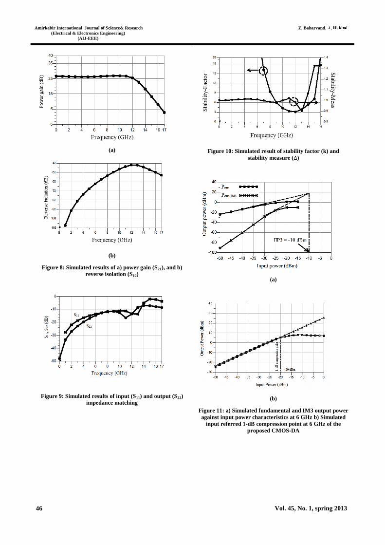
Figs. 8 ~ 12 show the simulated frequency responses
of the proposed CMOS-DA. As it can be seen from these
figures, the power gain is about 26.5 dB with a gain
flatness of ± 0.4 dB (Fig. 8 (a)). The DA exhibits a 3-dB
bandwidth of 13 GHz. The reverse isolation of the
proposed DA is less than - 40 dB over the amplifier’s
corresponding bandwidth (Fig. 8 (b)). Also, the simulated
input and output return losses both are better than - 11 dB
over the entire frequency band (Fig. 9).
The valuable measures of the stability called rollett
stability factor (or K-factor) and the stability measure. If
K-factor to be greater than one and the stability measure
( ) to be greater than zero and less than one imply that
the amplifier is unconditionally stable [21]. Fig. 10 shows
the simulated characteristics of k and against frequency
of the CMOS-DA. As it can be seen, the CMOS-DA is
unconditionally stable for frequencies from DC up to 13
GHz.
Linearity in CMOS-DA is typically evaluated in terms
of input third intercept point (IIP3) which is required to
be maximized. Two-tone testing is carried out with 1-
MHz spacing for third-order inter-modulation distortion
shown in Fig. 11 (a), the IIP3 simulated result is – 10
dBm at 6 GHz. Also, simulated input referred 1-dB
compression point at 6 GHz is illustrated in Fig. 11 (b)
that achieves the value of -20 dBm. Finally, Fig. 12
illustrates the simulated eye-diagram of this design. The
most important eye-diagram parameters are summarized
in Table 1.
Until now, distinctive DA design techniques are
demonstrated that each of them enhances one of the DA
design parameters. As a consequence, a figure-of-merit
(FOM) is defined to evaluate the most important
parameters in DAs designing, containing power
dissipation, noise, gain and bandwidth [6, 22]:
[ ⁄ ]
[ ] [ ]
[ ] [ ] (40)
Where [1] illustrates the average power gain in
magnitude, BW [GHz] refers to the 3-dB bandwidth in
gigahertz, (NF - 1) [1] presents the excess NF in
magnitude and [mW] demonstrates power
consumption in milli watts. This FOM contains the most
related parameters to investigate DAs for low-power,
high gain, low-noise, and wideband applications [6].
Amirkabir International Journal of Science& Research
(Electrical & Electronics Engineering)
(AIJ-EEE)
Z. Baharvand
Vol. 45, No. 1, spring 2013 46
(a)
(b)
Figure 8: Simulated results of a) power gain (S21), and b)
reverse isolation (S12)
Figure 9: Simulated results of input (S11) and output (S22)
impedance matching
Figure 10: Simulated result of stability factor (k) and
stability measure ( )
(a)
(b)
Figure 11: a) Simulated fundamental and IM3 output power
against input power characteristics at 6 GHz b) Simulated
input referred 1-dB compression point at 6 GHz of the
proposed CMOS-DA

Amirkabir International Journal of Science& Research
(Electrical & Electronics Engineering)
(AIJ-EEE)
Analysis and Design of High Gain, and Low Power CMOS Distributed
Amplifier Utilizing a Novel Gain-cell based on Combining Inductively Peaking
and Regulated Cascode Concepts
Vol. 45, No. 1, spring 2013 47
Figure12: Simulated eye diagram of the proposed CMOS-
DA
Table 1
Simulated Eye Parameters
Eye height 0.909
Eye width 4.566E-10
Eye Jitter (PP) 4.998E-11
Eye opening factor 0.975
Table 2 compares the performance of the presented
CMOS-DA with other broadband CMOS-DAs. The
presented DA has a high gain and low power dissipation
performance, at the same time.
Table 2
Previously Published CMOS-DAs against the Proposed CMOS-DA References Process Freq
(GHz)
Gain
(dB)
S11
(dB)
S22
(dB)
PDC
(mw)
FOM
(GHz/mW)
[23]2013a 0.18μm
CMOS
32 9.5 <-15 <-10 71 0.44
[5]2011a
(HG mode)
0.18μm
CMOS 1.5~8.2 17.1 ± 1.5 <-11 <-10.1 46.85 0.7
[5]2011a
(LG mode)
0.18μm
CMOS 1.2~ 8.6 11.4 ± 1.4 <-9.4 <-10.4 9.85 1.72
[3]2011a 0.18μm
CMOS
35 20.5 <-12 <-14 250 0.34
[7]2013b
(HG mode)
0.13μm
CMOS 0~11 20.5 ± 0.5 <-11 <-18 9.36 2.95
[7]2013b
(LG mode)
0.13μm
CMOS 0~12 15.5 ± 0.25 <-11.5 <-16.5 3.6 5
[6]2011b
(HG mode)
0.13μm
CMOS 0.4~10.5 20.47 ± 0.72 <-10 <-10 37.8 1.73
[6]2011b
(LG mode)
0.13μm
CMOS 0.7~10.9 11.03 ± 0.98 <-10.3 <-10.9 6.86 2.67
[20]2014b 0.13μm
CMOS 3.1~10.5 29.4 <-10 <-10 61 3.78
This workb
0.13μm
CMOS DC ~ 13 26.5 ± 0.4 <-11.1 <-11.3 9.95 10.02
This workc
0.13μm
CMOS DC ~ 13 26.5 ± 1.5 <-11.1 <-10 9.95 10.02
a: Based on the measurement results b: Based on the simulation results c: Based on the MC simulation results
To author’s knowledge, this circuit reports one of the
good FOM among the reported DAs covering ultra-wide-
band (UWB) ranges of frequencies (3.1 to 10.6 GHz) in
0.18 μm and 0.13 μm CMOS processes. The high value
of the FOM implicates to this fact that the new design
exhibits a good combination of gain, bandwidth, NF, and
power consumption. Thanks to the operation from DC up
to 13 GHz in conjunction with the high gain and low
power consumption characterizes, this CMOS-DA design
can be used in various ultra-broad band applications.
B- MC Simulation Results
The first step of the actual modeling of the proposed
design is to consider the non-ideal properties which are
unavoidable in practice. They have been known as,
possible fluctuations in MOS parameters such as ,
effective gate length , thickness of the gate oxide ,
and the drain-source region parasitic resistance [24]
and also, the variations of supply voltage and the
tolerance of passive components like inductors and
resistors.
To take into account the risks associated with various
input parameters which they receive little or no
consideration in simulating of designs utilizing ideal

Amirkabir International Journal of Science& Research
(Electrical & Electronics Engineering)
(AIJ-EEE)
Z. Baharvand
Vol. 45, No. 1, spring 2013 48
components, the MC simulation is appropriate option.
Whereas, in MC simulation a tolerance range is
considered for each of inputs. In the other words, MC
simulation relies on a repetitive process of inputs value
random sampling from their specified tolerance range,
simulating of the design finally, getting a set of output
parameters to obtain an estimation of the accuracy
performance of the proposed design under various
conditions [25]. A set of random inputs with normal
(Gaussian) distribution in the range of their possible
values are generated by ADS simulation tool, note that
the Gaussian distribution models the worst case of
possible situation. Then, the proposed design is simulated
by running multiple trial runs, (e.g., 1000).
Ultimately, a set of output parameters are yielded. Now, it
is possible to determine a number of non-ideal properties
which may appear in real implementation of the proposed
CMOS-DA. In this design, the tolerance of the passive
component including inductors, and resistors take into
account. The fluctuations in MOS parameters belong to
0.13 μm CMOS technology are given according to Table
3.
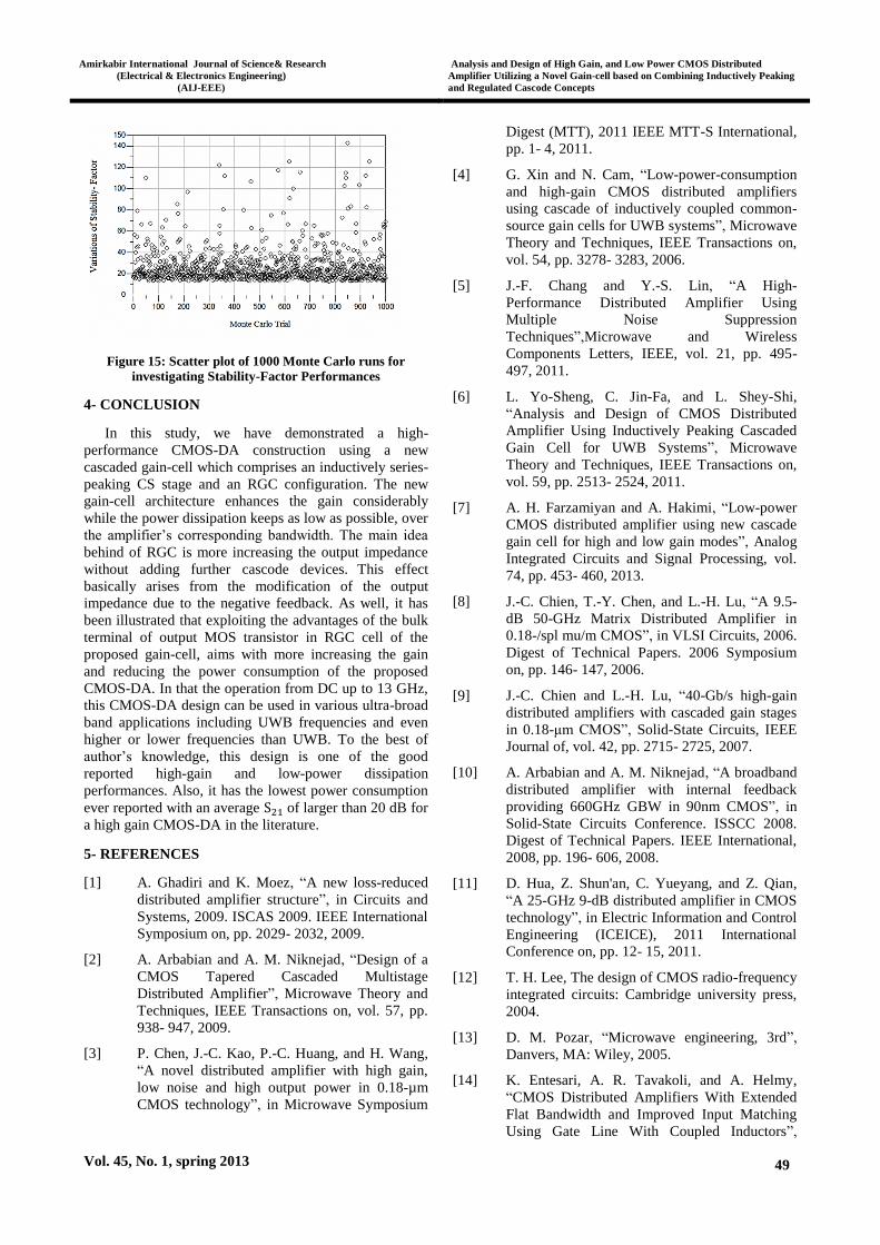
Figs. 13 ~ 15 illustrate the effects of input’s uncertainty
on performance of the proposed CMOS-DA including S-
parameters, and stability factor responses. As it can be
seen from these figures, within 1000 MC trail runs the
revers isolation (Fig. 14 (b)), input and output
impedances matching (Fig. 15 (a), (b)), and stability
factor (Fig. 16) responses demonstrate the better results
than original simulation. Also, the density of results
around of 26.5 dB as shown in Fig. 14 (a) validates the
accuracy of the power gain response, while only a few
numbers of the results will fail, which they can be
tolerated.
In this way, MC simulation predicts an estimate of the
good accuracy performance of the proposed design under
various conditions, in view of the fact that the MC and
original simulation results show a good agreement. Table
3 Parameter Values and ±3σ Variations of MOS transistor
[24]. Table 3
Parameter Values and ±3σ Variations of MOS transistor
[24]
Technology 0.13 µm
Parameters nmos pmos
0.09 ±
15%
0.09 ± 15%
33 ±
4%
33 ± 4%
0.33 ±
15.5%
- 0.33 ±
15.5% ⁄ 200 ±
10%
400 ± 10%
1.3 ± 10%
(a)
(b)
Figure 13: Scatter plot of 1000 Monte Carlo runs for
investigating a) Power Gain and b) Reverse Isolation
Performances
(a)
(b)
Figure 14: Scatter plot of 1000 Monte Carlo runs for
investigating a) Input Matching and b) Output Matching
Performances
Amirkabir International Journal of Science& Research
(Electrical & Electronics Engineering)
(AIJ-EEE)
Analysis and Design of High Gain, and Low Power CMOS Distributed
Amplifier Utilizing a Novel Gain-cell based on Combining Inductively Peaking
and Regulated Cascode Concepts
Vol. 45, No. 1, spring 2013 49
Figure 15: Scatter plot of 1000 Monte Carlo runs for
investigating Stability-Factor Performances
4- CONCLUSION
In this study, we have demonstrated a high-
performance CMOS-DA construction using a new
cascaded gain-cell which comprises an inductively series-
peaking CS stage and an RGC configuration. The new
gain-cell architecture enhances the gain considerably
while the power dissipation keeps as low as possible, over
the amplifier’s corresponding bandwidth. The main idea
behind of RGC is more increasing the output impedance
without adding further cascode devices. This effect
basically arises from the modification of the output
impedance due to the negative feedback. As well, it has
been illustrated that exploiting the advantages of the bulk
terminal of output MOS transistor in RGC cell of the
proposed gain-cell, aims with more increasing the gain
and reducing the power consumption of the proposed
CMOS-DA. In that the operation from DC up to 13 GHz,
this CMOS-DA design can be used in various ultra-broad
band applications including UWB frequencies and even
higher or lower frequencies than UWB. To the best of
author’s knowledge, this design is one of the good
reported high-gain and low-power dissipation
performances. Also, it has the lowest power consumption
ever reported with an average of larger than 20 dB for
a high gain CMOS-DA in the literature.
5- REFERENCES
[1] A. Ghadiri and K. Moez, “A new loss-reduced
distributed amplifier structure”, in Circuits and
Systems, 2009. ISCAS 2009. IEEE International
Symposium on, pp. 2029- 2032, 2009.
[2] A. Arbabian and A. M. Niknejad, “Design of a
CMOS Tapered Cascaded Multistage
Distributed Amplifier”, Microwave Theory and
Techniques, IEEE Transactions on, vol. 57, pp.
938- 947, 2009.
[3] P. Chen, J.-C. Kao, P.-C. Huang, and H. Wang,
“A novel distributed amplifier with high gain,
low noise and high output power in 0.18-µm
CMOS technology”, in Microwave Symposium
Digest (MTT), 2011 IEEE MTT-S International,
pp. 1- 4, 2011.
[4] G. Xin and N. Cam, “Low-power-consumption
and high-gain CMOS distributed amplifiers
using cascade of inductively coupled common-
source gain cells for UWB systems”, Microwave
Theory and Techniques, IEEE Transactions on,
vol. 54, pp. 3278- 3283, 2006.
[5] J.-F. Chang and Y.-S. Lin, “A High-
Performance Distributed Amplifier Using
Multiple Noise Suppression
Techniques”,Microwave and Wireless
Components Letters, IEEE, vol. 21, pp. 495-
497, 2011.
[6] L. Yo-Sheng, C. Jin-Fa, and L. Shey-Shi,
“Analysis and Design of CMOS Distributed
Amplifier Using Inductively Peaking Cascaded
Gain Cell for UWB Systems”, Microwave
Theory and Techniques, IEEE Transactions on,
vol. 59, pp. 2513- 2524, 2011.
[7] A. H. Farzamiyan and A. Hakimi, “Low-power
CMOS distributed amplifier using new cascade
gain cell for high and low gain modes”, Analog
Integrated Circuits and Signal Processing, vol.
74, pp. 453- 460, 2013.
[8] J.-C. Chien, T.-Y. Chen, and L.-H. Lu, “A 9.5-
dB 50-GHz Matrix Distributed Amplifier in
0.18-/spl mu/m CMOS”, in VLSI Circuits, 2006.
Digest of Technical Papers. 2006 Symposium
on, pp. 146- 147, 2006.
[9] J.-C. Chien and L.-H. Lu, “40-Gb/s high-gain
distributed amplifiers with cascaded gain stages
in 0.18-μm CMOS”, Solid-State Circuits, IEEE
Journal of, vol. 42, pp. 2715- 2725, 2007.
[10] A. Arbabian and A. M. Niknejad, “A broadband
distributed amplifier with internal feedback
providing 660GHz GBW in 90nm CMOS”, in
Solid-State Circuits Conference. ISSCC 2008.
Digest of Technical Papers. IEEE International,
2008, pp. 196- 606, 2008.
[11] D. Hua, Z. Shun'an, C. Yueyang, and Z. Qian,
“A 25-GHz 9-dB distributed amplifier in CMOS
technology”, in Electric Information and Control
Engineering (ICEICE), 2011 International
Conference on, pp. 12- 15, 2011.
[12] T. H. Lee, The design of CMOS radio-frequency
integrated circuits: Cambridge university press,
2004.
[13] D. M. Pozar, “Microwave engineering, 3rd”,
Danvers, MA: Wiley, 2005.
[14] K. Entesari, A. R. Tavakoli, and A. Helmy,
“CMOS Distributed Amplifiers With Extended
Flat Bandwidth and Improved Input Matching
Using Gate Line With Coupled Inductors”,

Amirkabir International Journal of Science& Research
(Electrical & Electronics Engineering)
(AIJ-EEE)
Z. Baharvand
Vol. 45, No. 1, spring 2013 50
Microwave Theory and Techniques, IEEE
Transactions on, vol. 57, pp. 2862- 2871, 2009.
[15] P. Heydari, “Design and Analysis of a
Performance-Optimized CMOS UWB
Distributed LNA”, Solid-State Circuits, IEEE
Journal of, vol. 42, pp. 1892- 1905, 2007.
[16] B. Razavi, Design of analog CMOS integrated
circuits: Tata McGraw-Hill Education, 2002.
[17] B. Razavi, Fundamentals of microelectronics
vol. 1: Wiley Hoboken, 2008.
[18] K. Moez and M. Elmasry, “A New Loss
Compensation Technique for CMOS Distributed
Amplifiers”, Circuits and Systems II: Express
Briefs, IEEE Transactions on, vol. 56, pp. 185-
189, 2009.
[19] D. A. Neamen, “Semiconductor physics and
devices”, 1992, 1994.
[20] M. Zakerhaghighi and A. Hakimi, “A Novel
Topology of Variable Gain Distributed
Amplifier in 0.13 μm CMOS Technology for
UWB Applications”, Electronic Components
and Materials, vol. 44, pp. 75- 83, 2014.
[21] J.-F. Chang and Y.-S. Lin, “DC∼ 10.5 GHz
complimentary metal oxide semiconductor
distributed amplifier with RC gate terminal
network for ultra-wideband pulse radio
systems”, IET microwaves, antennas &
propagation, vol. 6, pp. 127- 134, 2012.
[22] D. Barras, F. Ellinger, H. Jackel, and W. Hirt,
“A low supply voltage SiGe LNA for ultra-
wideband frontends”, Microwave and Wireless
Components Letters, IEEE, vol. 14, pp. 469-
471, 2004.
[23] H. Chih-Yin, S. Tzu-Yu, and S. S. H. Hsu,
“CMOS Distributed Amplifiers Using
Gate–Drain Transformer Feedback
Technique”, Microwave Theory and Techniques,
IEEE Transactions on, vol. 61, pp. 2901- 2910,
2013.
[24] V. Venkatraman and W. Burleson, “Impact of
process variations on multi-level signaling for
on-chip interconnects”, in VLSI Design, 2005.
18th
International Conference on, pp. 362- 367,
2005.
[25] S. Raychaudhuri, “Introduction to monte carlo
simulation”, in Simulation Conference WSC
2008. Winter, 2008, pp. 91- 100, 2008.