analysis and design of matrix converters for adjustable …
TRANSCRIPT

ANALYSIS AND DESIGN OF MATRIX CONVERTERS FOR ADJUSTABLE
SPEED DRIVES AND DISTRIBUTED POWER SOURCES
A Dissertation
by
HAN JU CHA
Submitted to the Office of Graduate Studies of Texas A&M University
in partial fulfillment of the requirements for the degree of
DOCTOR OF PHILOSOPHY
August 2004
Major Subject: Electrical Engineering
brought to you by COREView metadata, citation and similar papers at core.ac.uk
provided by Texas A&M Repository

ANALYSIS AND DESIGN OF MATRIX CONVERTERS FOR ADJUSTABLE
SPEED DRIVES AND DISTRIBUTED POWER SOURCES
A Dissertation
by
HAN JU CHA
Submitted to Texas A&M University in partial fulfillment of the requirements
for the degree of
DOCTOR OF PHILOSOPHY
Approved as to style and content by:
______________________________ _____________________________ Prasad N. Enjeti Shankar Bhattacharyya (Chair of Committee) (Member)
______________________________ _____________________________ Hamid A. Toliyat Emil J. Straube (Member) (Member)
_____________________________ Chanan Singh (Head of Department)
August 2004
Major Subject: Electrical Engineering

iii
ABSTRACT
Analysis and Design of Matrix Converters for Adjustable Speed Drives
and Distributed Power Sources. (August 2004)
Han Ju Cha, B.S., Seoul National University, Seoul, Korea;
M.S., Pohang Institute of Science & Technology, Pohang, Korea
Chair of Advisory Committee: Dr. Prasad N. Enjeti
Recently, matrix converter has received considerable interest as a viable
alternative to the conventional back-to-back PWM (Pulse Width Modulation) converter
in the ac/ac conversion. This direct ac/ac converter provides some attractive
characteristics such as: inherent four-quadrant operation; absence of bulky dc-link
electrolytic capacitors; clean input power characteristics and increased power density.
However, industrial application of the converter is still limited because of some practical
issues such as common mode voltage effects, high susceptibility to input power
disturbances and low voltage transfer ratio. This dissertation proposes several new
matrix converter topologies together with control strategies to provide a solution about
the above issues.
In this dissertation, a new modulation method which reduces the common mode
voltage at the matrix converter is first proposed. The new method utilizes the proper zero
vector selection and placement within a sampling period and results in the reduction of
the common mode voltage, square rms of ripple components of input current and
switching losses.
Due to the absence of a dc-link, matrix converter powered ac drivers suffer from
input voltage disturbances. This dissertation proposes a new ride-through approach to
improve robustness for input voltage disturbances. The conventional matrix converter is

iv
modified with the addition of ride-through module and the add-on module provides ride-
through capability for matrix converter fed adjustable speed drivers.
In order to increase the inherent low voltage transfer ratio of the matrix
converter, a new three-phase high-frequency link matrix converter is proposed, where a
dual bridge matrix converter is modified by adding a high-frequency transformer into
dc-link. The new converter provides flexible voltage transfer ratio and galvanic isolation
between input and output ac sources.
Finally, the matrix converter concept is extended to dc/ac conversion from ac/ac
conversion. The new dc/ac direct converter consists of soft switching full bridge dc/dc
converter and three phase voltage source inverter without dc link capacitors. Both
converters are synchronized for zero current/voltage switching and result in higher
efficiency and lower EMI (Electro Magnetic Interference) throughout the whole load
range. Analysis, design example and experimental results are detailed for each proposed
topology.

v
To my mother:
Jeong Hyea Kim,
for her sacrifice, trust, and for all the beautiful things she has taught me.
To my beloved family:
San Ra Kim,
Michael DongWon and Andy DongHyun
who are always deep in my heart.

vi
ACKNOWLEDGMENTS
I would like to express my heartfelt gratitude to Dr. Enjeti for his inspiring
guidance and encouragement throughout the whole endeavor. I am fortunate to have
worked with him and witnessed his dedication to research as well as teaching. I
express my sincere appreciation to the other members of committee; Dr.
Bhattacharyya, Dr. Toliyat, Dr. Straube and Dr. Singh. My thanks are also extended
to the lab members at Texas A&M University.
Without my family’s sacrifice and support, this study would not have been
possible. I would like to thank my mother, brothers and sister for their unconditional
love and constant encouragement in all my endeavors.

vii
TABLE OF CONTENTS
CHAPTER Page I INTRODUCTION................................................................................ 1 1.1 AC/AC conversion ................................................................... 1 1.2 Indirect space vector modulation ............................................. 3 1.2.1 Indirect modulation principle .......................................... 5 1.2.2 Space vector modulation for the inverter stage............... 8 1.2.3 Space vector modulation for the rectifier stage............... 14 1.2.4 Indirect modulation for the entire matrix converter ........ 19 1.3 Review of previous works........................................................ 25 1.4 Research objectives .................................................................. 32 1.5 Dissertation outline .................................................................. 33 II A NEW PWM STRATEGY TO REDUCE COMMON MODE VOLTAGE……………………........................................................... 35 2.1 Introduction .............................................................................. 35 2.2 Common mode voltage in matrix converter............................. 36 2.3 PWM strategy........................................................................... 38 2.4 Harmonic performance............................................................. 41 2.4.1 Output voltage ................................................................. 41 2.4.2 Input current .................................................................... 43 2.5 Simulation results ..................................................................... 46 2.6 Experimental results ................................................................. 48 2.7 Conclusion................................................................................ 55 III RIDE-THROUGH CAPABILITY FOR INPUT VOLTAGE
DISTURBANCE .................................................................................. 56 3.1 Introduction .............................................................................. 56 3.2 Ride-through system in matrix converter................................. 57 3.2.1 Ride-through system configuration ................................. 58 3.2.2 Ride-through strategy...................................................... 59 3.3 Simulation results ..................................................................... 62 3.4 Experimental results ................................................................. 64 3.4.1 Hardware implementation ............................................... 65 3.4.2 Results using the ride-through module............................ 66

viii
CHAPTER Page 3.5 Alternative scheme................................................................... 71 3.6 Conclusion................................................................................ 73 IV HIGH-FREQUENCY LINK TO INCREASE VOLTAGE TRANSFER RATIO ............................................................................ 74 4.1 Introduction .............................................................................. 74 4.2 High-frequency link matrix converter...................................... 76 4.2.1 Proposed topology........................................................... 76 4.2.2 Variable speed source 3φ/1φ matrix converter................ 77 4.2.3 Utility interactive 1φ/3φ matrix converter....................... 82 4.2.4 HF transformer design consideration .............................. 82 4.3 Simulation results ..................................................................... 84 4.4 Experimental results ................................................................. 86 4.5 Conclusion................................................................................ 90 V SOFT SWITCHING DC/AC DIRECT CONVERTER ....................... 92 5.1 Introduction .............................................................................. 92 5.2 Power conditioner topology ..................................................... 93 5.3 PWM strategy in inverter stage................................................ 95 5.4 Soft switching strategy in dc/dc converter ............................... 97 5.4.1 ZCS turn-off operation .................................................... 98 5.4.2 ZVS turn-on operation .................................................... 99 5.4.3 Clamp circuit design consideration ................................. 100 5.5 Experimental results ................................................................. 101 5.6 Conclusion................................................................................ 105 VI CONCLUSIONS.................................................................................. 107 6.1 Conclusions .............................................................................. 107 6.2 Suggestions for future work ..................................................... 108 REFERENCES.............................................................................................. 110 VITA………….. ........................................................................................... 117

ix
LIST OF FIGURES
FIGURE Page
1.1 Ac/ac converter (a) indirect ac/ac converter (b) direct ac/ac converter..... 2
1.2 Three phase matrix converter.................................................................... 2
1.3 Matrix converter topology................. ....................................................... 4
1.4 Switching constraints (a) short circuit between input phases (b) open circuit for output phase.............................................................................. 4
1.5 The equivalent circuit for indirect modulation................. ........................ 6
1.6 Transformation from equivalent circuit to matrix converter in phase A… 8
1.7 Inverter stage from the equivalent circuit.……………………………….. 9
1.8 Inverter voltage hexagon …………………………….………………….. 11
1.9 Synthesis of reference voltage vector ………….…….………………….. 11
1.10 Six sectors in the output voltages ………….……………………………. 13
1.11 Rectifier stage from the equivalent circuit ………….………..…………. 14
1.12 Rectifier current hexagon ………………………..….………..…………. 16
1.13 Synthesis of reference current vector (mC = 1) ……………….…………. 17
1.14 Six sectors in input phase voltage ………………………..…..…………. 19
1.15 V1 – I1 pair during dβγ ………………………..….…………...…………... 22
1.16 V6 – I1 pair during dαγ ………………………..….…………...…………... 22
1.17 V6 – I2 pair during dαδ ………………………..….…………...……….…. 23
1.18 V1 – I2 pair during dβδ ………………………..….…………...……….…. 23
1.19 V0 – I0 pair during d0 ………………………..….…………….…………. 23
1.20 Space vector representation (a) 1st strategy (b) 2nd strategy……...…...…. 28
1.21 Operating modes during ride-through (a) charging mode (b) discharging mode..……..….…………….…………….. .......................... 30

x
FIGURE Page
2.1 Common mode voltage and leakage current path (a) three phase matrix converter (b) the model of the matrix converter for indirect modulation................................................................................................ 36
2.2 Zero vector component (a) the optimized ISVPWM (b) the proposed ISVPWM................. .................................................................................. 39
2.3 The per-carrier cycle rms value of the harmonic flux............................... 41
2.4 The harmonic flux as a function of the modulation index (solid line : proposed PWM, dashed line : optimized PWM ) ................. ................... 42
2.5 The per-carrier cycle rms value of the harmonic charge........................... 44
2.6 The harmonic charge as a function of the modulation index under output power factor=0.9 ( solid line : proposed PWM, dashed line : optimized PWM )................. ..................................................................... 45
2.7 The harmonic charge as a function of the modulation index under output power factor=0.6 ( solid line : proposed PWM, dashed line : optimized PWM )................. ..................................................................... 45
2.8 Waveform of Vcm with fout= 50Hz, mV= 0.83 (a) the conventional ISVPWM (b) the proposed ISVPWM..................................................... 46
2.9 Waveform of Vcm with fout = 20Hz , mV = 0.33 (a) the conventional ISVPWM (b) the proposed ISVPWM.................................................... 47
2.10 Block diagram of 3kVA matrix converter................................................. 48
2.11 3 kVA laboratory prototype matrix converter........................................... 49
2.12 Waveforms with fout = 50Hz , mV = 0.83 (a) the conventional ISVPWM (b) the proposed ISVPWM (ch 3:VAB and ch 4: Vcm)................. ............... 50
2.13 Waveforms with fout = 20Hz , mV = 0.33 (a) the conventional ISVPWM (b) the proposed ISVPWM (ch 3:VAB and ch 4: Vcm)................. ............... 51
2.14 Harmonic spectrum of Vcm with fout = 50Hz , mV = 0.83 (a) the conventional ISVPWM (b) the proposed ISVPWM................. .............. 52
2.15 Waveforms with fout = 50Hz , mV = 0.83 (a) the conventional ISVPWM (b) the proposed ISVPWM (ch 2: Ileakage (0.5A/div), ch 4: Vcm) ................. ................................................................................. 53

xi
FIGURE Page
2.16 Vcm comparisons of conventional PWM and proposed PWM (a) peak value (b) rms value................................................................................... 54
3.1 Matrix converter with ride-through module (SiA, SiB, SiC are add-on IGBTs)………………….......................................................................... 58
3.2 Operating mode (a) normal mode (b) ride-through mode......................... 60
3.3 Control block diagram for the ride-through strategy ................................ 62
3.4 Ride-through operation under no load torque (from top to bottom (a) input line voltage Vab (b) motor phase current IA (c) dc-link voltage Vdc (d) motor shaft speed [rpm]) ..................................................................... 63
3.5 Ride-through operation under 100% load torque (from top to bottom (a) input line voltage Vab (b) motor phase current IA (c) dc-link voltage
Vdc (d) motor shaft speed [rpm]) .............................................................. 64
3.6 Block diagram of 3kVA matrix converter with ride-through module ...... 65
3.7 3 kVA matrix converter with ride-through module .................................. 66
3.8 Matrix converter module operation (ch2 : input voltage Vab, ch3: output current IA [5A/div], ch4: output line-to-line voltage VAB ) ....................... 67
3.9 Ride-through module operation (ch2 : input voltage Vab, ch3: output current IA [5A/div], ch4: output line-to-line voltage VAB ) ....................... 67
3.10 Waveforms at power disturbance (a) normal mode (b) ride-through mode (c) mode transition from ride-through mode to normal mode (ch1: STPI, ch2: output line-to-line voltage VAB, ch3 : input voltage Vab, ch4: output current IA [5A/div]) ........................................... 69
3.11 Comparison during power interruption (a) without ride-through module (b) with ride-through module (ch1: STPI, ch2: output current IA [5A/ div]), ch3: input voltage Vab, ch4: output line-to-line voltage VAB) .......... 70
3.12 Mode changes between normal mode and ride-through mode (ch1: STPI detector signal (0: normal mode, 1: ride-through mode), ch2: output frequency fOUT, ch3: input voltage Vab, ch4: output current IA ) ... 71
3.13 Modified voltage clamp circuit for ride-through capability...................... 72
4.1 (a) proposed 3φ/3φ high frequency link matrix converter (b) bidirectional switch configuration ........................................................... 76

xii
FIGURE Page
4.2 Real implementation of the proposed matrix converter ............................ 77
4.3 Six modes of input phase voltages ............................................................ 78
4.4 PWM pattern generation (a) duty cycle in input phase voltage (b) 50% duty square wave in the primary voltage VP (c) fluctuated dc-link voltage Vdc ….. .......................................................................................... 80
4.5 (a) equivalent circuit model (b) phasor diagram when displacement factor is 1.0…............................................................................................ 84
4.6 Primary side 3φ/1φ matrix converter waveforms (fin = 30 Hz) ................. 85
4.7 Secondary side 1φ/3φ matrix converter waveforms (fout = 60 Hz)............ 85
4.8 High frequency link waveforms at 60Hz input (ch2: Vp, ch3: Vab, ch4: Vdc ) ……........................................................................................... 87
4.9 Primary side waveforms at 60Hz input (ch2: Ia (10A/div), ch3: Va ) ...... 87
4.10 Input/out waveforms at 60Hz input (ch1: IA (20A/div), ch2: Ia (20A/div), ch3: VA, ch4: Vdc ) ................................................................... 88
4.11 FFT results at 60Hz input (ch M1: Ia, ch M2: IA )..................................... 88
4.12 High frequency link waveforms at 400Hz input (ch1: mode, ch2: Vp, ch3: Vab, ch4: Vdc ).................................................................................... 89
4.13 Input/out waveforms at 400Hz (ch1: IA (20A/div), ch2: Ia (20A/div), ch3: VA, ch4: Va )....................................................................................... 89
5.1 The proposed AC link based fuel cell power conditioner.......................... 93
5.2 The proposed 1φ/3φ direct converter for resident power system .............. 94
5.3 The proposed 1φ/3φ direct converter for 3φ utility interface .................... 95
5.4 PWM patterns at θ = 90º and zero vector position..................................... 96
5.5 (a) equivalent circuit at ZCS turn-off and (b) IS during inverter zero vectors ………........................................................................................... 99
5.6 3kVA direct matrix converter .................................................................... 101
5.7 ZVS turn on operation (ch1: S1 gate signal, ch3: S4DS, ch4: S4GE) ........... 102
5.8 ZCS operation with θ = 270º, unbalanced load (ch2: Is (5A/div), ch3: Vs, ch4: VUV) ….......................................................................................... 103

xiii
FIGURE Page
5.9 Inverter output voltage under unbalanced load (ch2: IA (10A/div), ch3: VAN, ch4: VBN ) …....................................................................................... 104
5.10 Snubber capacitor CS initial charge (ch3: VS, ch4: VC) .............................. 105

xiv
LIST OF TABLES
TABLE Page
1.1 Switch states and switching vectors for the inverter side .......................... 10
1.2 Switch states and switching vectors for the rectifier side .......................... 16
1.3 Switching sequence at current sector = S0, voltage sector = S0................. 24
2.1 Maximum common mode voltage according to output voltage vector...... 38
2.2 Nine step vector sequence (current hexagon : 1 , voltage hexagon : 1)..... 39
2.3 Vector sequence of the proposed ISVPWM .............................................. 40
4.1 Switch states and corresponding voltage VP and Vdc according to
mode of input phase voltages ..................................................................... 79

1
CHAPTER I
INTRODUCTION
1.1 AC/AC conversion
Many parts of industrial application request ac/ac power conversion and ac/ac
converters take power from one ac system and deliver it to another with waveforms of
different amplitude, frequency, or phase. The ac/ac converters are commonly classified
into indirect converter which utilizes a dc link between the two ac systems and direct
converter that provides direct conversion. Indirect converter consists of two converter
stages and energy storage element, which convert input ac to dc and then reconverting dc
back to output ac with variable amplitude and frequency as shown in Fig. 1.1 (a). The
operation of these converter stages is decoupled on an instantaneous basis by means of
energy storage element and controlled independently, so long as the average energy flow
is equal. Therefore, the instantaneous power flow does not have to equal the
instantaneous power output. The difference between the instantaneous input and output
power must be absorbed or delivered by an energy storage element within the converter.
The energy storage element can be either a capacitor or an inductor.
However, the energy storage element is not needed in direct converter as shown
in Fig. 1.1 (b) [1]. In General, direct converter can be identified as three distinct
topological approaches. The first and simplest topology can be used to change the
amplitude of an ac waveform. It is known as an ac controller and functions by simply
chopping symmetric notches out of the input waveform. The second can be utilized if the
output frequency is much lower than the input source frequency. This topology is called
a cycloconverter, and it approximates the desired output waveform by synthesizing it
This dissertation follows the style of IEEE Transactions on Industry Applications.

2
ACAC
(a) (b)
Fig. 1.1 Ac/ac converter (a) indirect ac/ac converter (b) direct ac/ac converter
from pieces of the input waveform. The last is matrix converter and it is most versatile
without any limits on the output frequency and amplitude. It replaces the multiple
conversion stages and the intermediate energy storage element by a single power
conversion stage, and uses a matrix of semiconductor bidirectional switches, with a
switch connected between each input terminal to each output terminal as shown in Fig.
1.2
3-PhaseAC load
Bidirectionalswitch
3-Phaseinput
Fig. 1.2 Three phase matrix converter
With this general arrangement of switches, the power flow through the converter
can reverse. Because of the absence of any energy storage element, the instantaneous
power input must be equal to the power output, assuming idealized zero-loss switches.
However, the reactive power input does not have to equal the reactive power output. It

3
can be said again that the phase angle between the voltages and currents at the input can
be controlled and does not have to be the same as at the output. Also, the form and the
frequency at the two sides are independent, in other words, the input may be three-phase
ac and the output dc, or both may be dc, or both may be ac [2]. Therefore, the matrix
converter topology is promising for universal power conversion such as: ac to dc, dc to
ac, dc to dc or ac to ac.
1.2 Indirect space vector modulation
In many ac drive applications, it is desirable to use a compact voltage source
converter to provide sinusoidal output voltages with varying amplitude and frequency,
while drawing sinusoidal input currents with unity power factor from the ac source, and
having high power density and efficiency. In recent years, matrix converter has become
increasingly attractive for these applications because they fulfill all the requirements,
having the potential to replace the conventionally used rectifier - dc-link - inverter
structures. Matrix converter is a single stage converter and they need no energy storage
components except small input ac filters for elimination of switching ripples.
However, a practical industrial application is still limited and the modulation
method for the matrix converter is also understood to limited engineering people because
of the high level of complexity and limited materials to explain its operating principle
easily. Meanwhile, the standard voltage source inverter (VSI) and its relevant space
vector modulation (SVM) are well known to many engineering people due to the
opposite reasons. Therefore, it would be a good approach to explain the operating
principle of the matrix converter by adopting standard VSI topology and SVM concept.
The simplified 3φ-3φ matrix converter topology is shown in Fig. 1.3. Matrix
converter consists of nine bidirectional switches and each output phase is associated with
three switch set connected to three input phases. This configuration of bidirectional

4
M
A
B
C
a
bc
SaA
SbA
ScA
SaB
SbB
SbC
SaC
SbC
ScC Fig.1.3 Matrix converter topology
switches enables to connect any of input phase a, b, or c to any of output phase A, B or C
at any instant. Since the matrix converter is supplied by the voltage source, the input
phases must not be shorted and due to the inductive nature of the load, the output phases
must not be open. These constraints are illustrated for the switch set connected to the
output phase A in Fig 1.4.
If the switch function of a switch Sij in Fig. 1 is defined as [3]
Sij (t) = 1, Sij closed i ∈a, b, c, j ∈A, B, C (1.1)
0, Sij open
the constraints can be expressed as
Saj + Sbj + Scj = 1, j ∈A, B, C (1.2)
Aabc
SaA
SbA
ScA
Input phase a & b are short
Aabc
SaA
SbA
ScA
Output phase A is open (a) (b)
Fig. 1.4 Switching constraints (a) short circuit between input phases (b) open circuit for
output phase

5
Regarding these two basic rules, the number of legal switch states reduces to 27 (33) and
each switch state can be characterized by a three letter code. The three letter codes
describe which output phase is connected to which input phase. For instance, the switch
state named [aba] refers to the state where output phase A is connected to input phase a,
output phase B is to input phase b and output phase C is to input phase a.
1.2.1 Indirect modulation principle
The object of the modulation strategy is to synthesize the output voltages from
the input voltages and the input currents from the output currents. The three phase matrix
converter can be represented by a 3 by 3 matrix form because the nine bidirectional
switches can connect one input phase to one output phase directly without any
intermediate energy storage elements. Therefore, the output voltages and input currents
of the matrix converter can be represented by the transfer function T and the transposed
TT such as
VO = T * VI
⋅
=
c
b
a
cCbCaC
cBbBaB
cAbAaA
C
B
A
VVV
SSSSSSSSS
VVV
(1.3)
II = TT * IO
⋅
=
C
B
A
cCcBcA
bCbBbA
aCaBaA
c
b
a
III
SSSSSSSSS
III
(1.4)
where Va, Vb and Vc are input phase voltages, VA, VB and VC are output phase voltages, Ia,
Ib and Ic are input currents and IA, IB and IC are output currents. The elements in the
transfer matrix Tij represent the switch function from the instantaneous input voltage Vi
to the instantaneous output voltage Vj and have to be assigned values that assure output

6
voltages and input currents to follow their reference values. Defining a modulation
strategy is actually filling in the elements of the transfer matrix. Although several
modulation strategies have been proposed since Venturini announced a closed
mathematical solution for the transfer function T in early 1980, the indirect space vector
modulation is gaining as a standard technique in the matrix converter modulations.
MABC
abc
VDC+
VDC-
VDC
IDC-
Rectifying Stage Inverting stage
IDC+S1
S2
S3
S4
S5
S6
S7
S8
S9
S10
S11
S12
Fig.1.5 The equivalent circuit for indirect modulation
The indirect space vector modulation (indirect SVM) was first proposed by
Borojevic et al in 1989 where matrix converter was described to an equivalent circuit
combining current source rectifier and voltage source inverter connected through virtual
dc link as shown in Fig. 1.5. Inverter stage has a standard 3φ voltage source inverter
topology consisting of six switches, S7 ~ S8 and rectifier stage has the same power
topology with another six switches, S1 ~ S6. Both power stages are directly connected
through virtual dc-link and inherently provide bidirectional power flow capability
because of its symmetrical topology. Although this equivalent circuit has provided a
strong platform to analyze and derive several extended PWM strategies specified in a
certain application since then, it is still ambiguous for a beginner to grasp its operating
principle. The operating principle of the indirect SVM will be illustrated with graphical
approach.

7
The basic idea of the indirect modulation technique is to decouple the control of
the input current and the control of the output voltage. This is done by splitting the
transfer function T for the matrix converter in (1.3) into the product of a rectifier and an
inverter transfer function.
T = I * R
⋅
=
642
531
1211
109
87
SSSSSS
SSSSSS
SSSSSSSSS
cCbCaC
cBbBaB
cAbAaA
(1.5)
where the matrix I is the inverter transfer function and the matrix R is the rectifier
transfer function. This way to model the matrix converter provides the basis to regard the
matrix converter as a back-to-back PWM converter without any dc-link energy storage.
This means the well know space vector PWM strategies for voltage source inverter
(VSI) or PWM rectifier can be applied to the matrix converter.
By substituting (1.5) into (1.3)
⋅
⋅
=
c
b
a
C
B
A
VVV
SSSSSS
SSSSSS
VVV
642
531
1211
109
87
⋅
⋅+⋅⋅+⋅⋅+⋅⋅+⋅⋅+⋅⋅+⋅
⋅+⋅⋅+⋅⋅+⋅
=
c
b
a
C
B
A
VVV
SSSSSSSSSSSSSSSSSSSSSSSS
SSSSSSSSSSSS
VVV
612511412311212111
610594103921019
685748372817
(1.6)
The above transfer matrix exhibits that the output phases are compounded by the
product and sum of the input phases through inverter switches S7 ~ S12 and rectifier
switches S1 ~ S6. The first row of (1.6) represents how output phase A is built from the
input phase a, b and c and this mathematical expression can be interpreted again in the
graphical viewpoint. If the equivalent circuit is seen from the inverter output phase A,
two switches S7 and S8 of phase A half bridge is directly connected to input phases a, b
and c through six rectifier switches S1 ~ S6. Fig. 1.7 shows how the switch set of
equivalent circuit can be transformed into the relevant switch set of the nine bidirectional
8
VA
Va
Vb
Vc
S1
S3
S5
S2
S4
S6
S7
S8VDC-
VDC+
VAVa
Vb
Vc
S7S1+S8S2
S7S3+S8S4
S7S5+S8S6
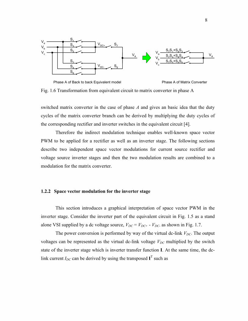
Phase A of Back to back Equivalent model Phase A of Matrix Converter Fig. 1.6 Transformation from equivalent circuit to matrix converter in phase A
switched matrix converter in the case of phase A and gives an basic idea that the duty
cycles of the matrix converter branch can be derived by multiplying the duty cycles of
the corresponding rectifier and inverter switches in the equivalent circuit [4].
Therefore the indirect modulation technique enables well-known space vector
PWM to be applied for a rectifier as well as an inverter stage. The following sections
describe two independent space vector modulations for current source rectifier and
voltage source inverter stages and then the two modulation results are combined to a
modulation for the matrix converter.
1.2.2 Space vector modulation for the inverter stage
This section introduces a graphical interpretation of space vector PWM in the
inverter stage. Consider the inverter part of the equivalent circuit in Fig. 1.5 as a stand
alone VSI supplied by a dc voltage source, VDC = VDC+ - VDC- as shown in Fig. 1.7.
The power conversion is performed by way of the virtual dc-link VDC. The output
voltages can be represented as the virtual dc-link voltage VDC multiplied by the switch
state of the inverter stage which is inverter transfer function I. At the same time, the dc-
link current IDC can be derived by using the transposed IT such as

9
M
VDC+
VDC-
VDC
IDC-
Inverting stage
IDC+ S7
S8
S9
S10
S11
S12
VA
VB
VC
IAIBIC
Fig. 1.7 Inverter stage from the equivalent circuit
⋅
=
−
+
DC
DC
C
B
A
VV
SSSSSS
VVV
1211
109
87
(1.7)
⋅
=
−
+
C
B
A
DC
DC
III
SSSSSS
II
12108
1197 (1.8)
Then the output voltage space vector VOUT and output current space vector IOUT
are expressed as space vectors using the transformation such as
)(32 3
43
2 ππ jC
jBAOUT eVeVVV ⋅+⋅+=
(1.9)
)(32 3
43
2 ππ jC
jBAOUT eIeIII ⋅+⋅+= (1.10)
The inverter switches, S7 ~ S12 can have only eight allowed combinations to avoid a short
circuit through three half bridges. The eight combinations can be divided into six
nonzero output voltages which are active vector V1 ~ V6 and two zero output voltages
which are zero vector V0. Table 1.1 lists the possible switch states and the relevant
voltage space vectors. In addition, the amplitude and angle of the output voltage space
vectors are evaluated for six active vectors and two zero vectors.

10
Table 1.1 Switch states and switching vectors for the inverter side
VA VB VC Type Vector T
SSSSSS
12108
1197
VAB VBC VCA outV outV∠ IDC+
2/3VDC - -1/3VDC V1[100]
T
110001 VDC 0 -VDC
DCV32 0 IA
1/3VDC 1/3VDC -2/3VDC V2[110]
T
100
011 0 VDC -VDC DCV
32
3π -IC
-1/3VDC 2/3VDC -1/3VDC V3[010]
T
101010 -VDC VDC 0
DCV32
32π IB
-2/3VDC 1/3VDC 1/3VDC V4[011]
T
001110 -VDC 0 VDC
DCV32 π -IA
-1/3VDC - 2/3VDC V5[001]
T
011100 0 -VDC VDC
DCV32
32π
− IC
1/3VDC - 1/3VDC
Active
V6[101] T
010101 VDC -VDC 0
DCV32
3π
− -IB
Zero V0[000]
[111]
T
111000 T
000111 0 0
The voltage space vector V1[100] indicates that output phase VA is connected to
positive rail VDC+ and the other phase VB, VC are connected to negative rail VDC- and its
vector magnitude is calculated from
6
34
32
34
32
1
32
)31
31
32(
32
)(32
π
ππ
ππ
jDC
jDC
jDCDC
jC
jBA
eV
eVeVV
eVeVVV
⋅=
⋅⋅−⋅⋅−⋅=
⋅+⋅+=
(1.11)
The discrete seven space vectors can be configured as a hexagon in a complex
plane shown in Fig. 1.8 and an arbitrary VOUT within the hexagon can be synthesized by
a vector sum out of seven discrete output voltage switching state vectors, V0 ~ V7.

11
V2 (110)
V1 (100)
V3 (010)
V4 (011)
V5 (001) V6 (101)
0
12
3
45
VC
VB
VA
Fig. 1.8 Inverter voltage hexagon
The maximum amplitude of the reference vector is equal to the radius of inner
circle of the hexagon whose radius is 23 (=0.866) times the amplitude of the active
vectors. Then the reference output voltage is build by applying the well-known space
vector modulation method based on the virtual dc-link, exactly as in a conventional VSI
inverter.
Vβ
Vα
Vo*
dαVα
dβVβ
θV
Fig. 1.9 Synthesis of reference voltage vector
Fig. 1.9 shows the reference voltage vector VO* within a sector of the voltage
hexagon. The VO* is synthesized by impressing the adjacent active vectors Vα and Vβ
with the duty cycles dα and dβ, respectively. If the output voltages are considered

12
constant during a short switching interval TS, the reference vector can be expressed by
the voltage-time product sum of the adjacent active vectors
ββαα VdVdVO ⋅+⋅=* (1.12)
The duration of the active vectors determines the direction of VO* while the zero
vector interval is used to adjust the amplitude of VO*. The duty cycle of the active
vectors is calculated by
)3
sin( VVS
mTTd θπα
α −⋅==
)sin( VVS
mTTd θα
β ⋅== (1.13)
βα ddTTd
SV
V −−== 100
where θV indicates the angle of the reference voltage vector within the actual hexagon
sector. The mV is the voltage modulation index and defines the desired voltage transfer
ratio such as
DC
OVV V
Vmm
*3,10
⋅=≤≤ (1.14)
where VDC is the averaged value of virtual dc-link voltage and derived as follows. Since
there is no energy storage in the converter, the averaged value of virtual dc-link voltage
VDC can be found on the basis that the input power flow and the dc power flow are equal
at any instant. Fundamental components are considered for the calculation under
balanced input voltage condition
INDC PP =
)cos(23
INININDCDC IVIV ϕ⋅⋅⋅=⋅
)cos(23
INDC
ININDC I
IVV ϕ⋅⋅⋅= (1.15)
)cos(23
INCINDC mVV ϕ⋅⋅⋅=
where VIN : the peak value of input phase voltage

13
IIN : the peak value of input current
φIN : input displacement angle
The virtual dc-link voltage VDC depends on the amplitude of input phase voltage,
the current modulation index mV and the input displacement angle φIN. Since the rectifier
stage is usually operated with the condition mC = 1 and unity input displacement angle
φIN = 0, the VDC become simplified to
INDC VV ⋅=23
The six sectors of the voltage hexagon in Fig. 1.8 correspond directly to the six
60º segments within a period of the desired 3φ output line voltages as shown in Fig.
1.10.
0 π/2−π/2 π ωt
VA VB VC
0 45 321V5 V4V3V2V1V6
Voltage SectorVoltage Vector
Fig. 1.10 Six sectors in the output voltages
The synthesis of the output phase voltages for a switching cycle within the
voltage sector S0 is chosen as an example. Since Vα is V6 and Vβ is V1 in the voltage
sector S0 in Fig. 1.8, the mean value of the output voltages and dc-link current can be
written as follows
⋅
⋅+
⋅=⋅+⋅=
−
+
DC
DC
C
B
A
VV
ddVdVdVVV
101001
011001
16 βαβα (1.16)

14
⋅
⋅+
⋅=
−
+
C
B
A
DC
DC
III
ddII
110001
010101
βα (1.17)
1.2.3 Space vector modulation for the rectifier stage
This section introduces a graphical interpretation of space vector PWM in the
rectifier stage. Likewise the case of inverter stage, the rectifier part of the equivalent
circuit in Fig. 1.5 can be assumed to a stand alone current source rectifier (CSR) loaded
by a dc current source, IDC as shown in Fig. 1.11.
Va
Vb
Vc
VDC+
VDC-
VDC
IDC-
Rectifying Stage
IDC+S1
S2
S3
S4
S5
S6
IaIbIc
Fig. 1.11 Rectifier stage from the equivalent circuit
In the indirect space vector modulation, all quantities are referred to virtual dc
link and the virtual dc-link is built by chops of the input voltages. The input currents can
be represented as the virtual dc-link current IDC multiplied by the switch state of the
rectifier stage which is rectifier transfer function R. At the same time, the dc-link voltage
VDC can be derived by using the transposed RT such as

15
⋅
=
−
+
DC
DC
c
b
a
II
SSSSSS
III
65
43
21
(1.18)
⋅
=
−
+
c
b
a
DC
DC
VVV
SSSSSS
VV
642
531 (1.19)
Then the input current space vector IIN and input voltage space vector VIN are expressed
as space vectors using the transformation such as
)(32 3
43
2 ππ jc
jbaIN eIeIII ⋅+⋅+= (1.20)
)(32 3
43
2 ππ jc
jbaIN eVeVVV ⋅+⋅+= (1.21)
The rectifier switches, S1 ~ S6 can have only nine allowed combinations to avoid
a open circuit at the dc link rails. The nine combinations can be divided into six nonzero
input currents which are active vector I1 ~ I6 and three zero input currents which are zero
vector I0. Table 1.2 lists the possible switch states and the relevant current space vectors.
In addition, the amplitude and angle of the input current space vectors are evaluated for
6 active vectors and 3 zero vectors.
I1 [ab] indicates that input phase a is connected to the positive rail of the virtual
dc-link VDC+ and input phase b is to the negative rail VDC-. Its vector magnitude is
calculated from
6
34
32
34
32
1
32
)0(32
)(32
π
ππ
ππ
jDC
jjDCDC
jc
jba
eI
eeII
eIeIII
−⋅=
⋅+⋅−=
⋅+⋅+=
(1.22)
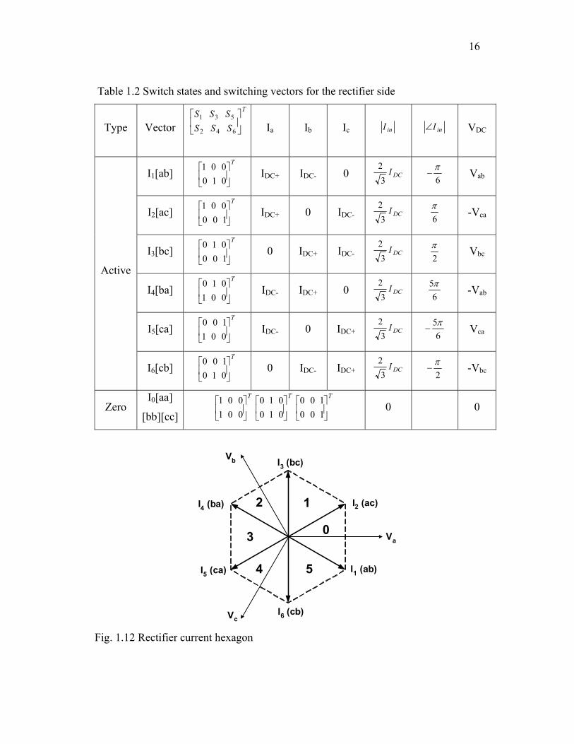
16
Table 1.2 Switch states and switching vectors for the rectifier side
Type Vector
T
SSSSSS
642
531
Ia Ib Ic inI inI∠ VDC
I1[ab] T
010001 IDC+ IDC- 0 DCI
32
6π
− Vab
I2[ac] T
100001 IDC+ 0 IDC- DCI
32
6π -Vca
I3[bc] T
100010 0 IDC+ IDC- DCI
32
2π Vbc
I4[ba] T
001010 IDC- IDC+ 0 DCI
32
65π -Vab
I5[ca] T
001100 IDC- 0 IDC+ DCI
32
65π
− Vca
Active
I6[cb] T
010100 0 IDC- IDC+ DCI
32
2π
− -Vbc
Zero I0[aa]
[bb][cc]
T
001001 T
010010 T
100100 0 0
I3 (bc)
I2 (ac)I4 (ba)
I5 (ca)
I6 (cb)
I1 (ab)
0
12
3
4 5
Va
Vb
Vc Fig. 1.12 Rectifier current hexagon

17
Iδ
Iγ
II*
dγIγ
dδIδ
θC
Fig. 1.13 Synthesis of reference current vector (mC = 1)
The discrete seven space vectors can be configured as a hexagon in a complex plane
shown in Fig. 1.12 and an arbitrary IIN within the hexagon can be synthesized by a vector
sum out of seven discrete input current switching state vectors, I0 ~ I6.
Fig. 1.13 shows the reference input current vector II* within a sector of the
current hexagon. The II* is synthesized by impressing the adjacent switching vectors Iγ
and Iδ with the duty cycles dγ and dδ, respectively. If the input currents are considered
constant during a short switching interval TS, the reference vector can be expressed by
the current-time product sum of the adjacent active vectors
δδγγ IdIdI I ⋅+⋅=* (1.23)
The duration of the active vectors determines the direction of II* while the zero
vector interval is used to adjust the amplitude of II*. The space vector modulation
(SVM) for rectifier is completely analogous to the SVM for inverter. The inverter
subscript α, β and mV are replaced with the subscript γ, δ and mC for rectifier,
respectively. Thus, the duty cycle of the active vectors are written as
)3
sin( CCS
mTTd θπγ
γ −⋅==
)sin( CCS
mTTd θδ
δ ⋅== (1.24)
δγ ddTTd
SC
C −−== 100

18
where θC indicates the angle of the reference current vector within the actual hexagon
sector. The mC is the current modulation index and defines the desired current transfer
ratio such as
DC
ICC I
Imm
*,10 =≤≤ (1.25)
The current modulation index mC is often fixed to unity and the voltage
modulation index mV is variable according to a required overall voltage transfer gain. In
addition, IDC is the averaged value of virtual dc-link current and derived as follows.
Since there is no energy storage in the converter, the averaged value of virtual dc-link
current IDC can be derived on the basis that the output power flow equals the dc power
flow at any instant. Fundamental components are considered for the calculation together
with balanced output load current condition such as
OUTDC PP =
)cos(23
OUTOUTOUTDCDC IVIV ϕ⋅⋅⋅=⋅
)cos(23
OUTDC
OUTOUTDC V
VII ϕ⋅⋅⋅= (1.26)
)cos(23
OUTVOUTDC mII ϕ⋅⋅⋅=
where VOUT : the peak value of output phase voltage
IOUT : the peak value of output current
φOUT : output load displacement angle
The virtual dc-link current IDC depends on the amplitude of output load current,
the voltage modulation index mC and the output load displacement angle φOUT. Under
steady state, IDC is assumed to be constant. The rectifier has to generate a dc-link voltage
from the input voltages. At the same time, the rectifier has to assure the input currents to
be sinusoidal with a controllable displacement angle with respect to the input voltage
system. In other words, the input currents should be synchronized to the input voltage

19
0 π/2−π/2 π ωt
Va Vb Vc
0 45 3214I6 I5I4I3I2I1
Current Sector
Current Vector
Fig. 1.14 Six sectors in input phase voltage
system with a desired displacement angle. Therefore the sectors of the current hexagon
in Fig. 1.12 can be mapped directly to the six 60º segments of input phase voltage within
a period of the given 3φ input phase voltages as shown in Fig. 1.14.
The synthesis of the input current for a switching cycle within the current sector
S0 is chosen as an example. Since Iγ is I1 and Iδ is I2 in the current sector S0, the mean
value of the input currents and dc-link voltage can be written as follows
⋅
⋅+
⋅=⋅+⋅=
−
+
DC
DC
c
b
a
II
ddIdIdIII
100001
001001
21 δγδγ (1.27)
⋅
⋅+
⋅=
−
+
c
b
a
DC
DC
VVV
ddVV
100001
010001
δγ (1.28)
1.2.4 Indirect modulation for the entire matrix converter
Although the duty cycles and relevant switching vectors are derived from
rectifier stage and inverter stage in the previous sections, respectively, these are only
meaningful in the equivalent circuit of matrix converter or dual bridge matrix converter
[5]. Therefore, two independent space vector modulations should be merged into one

20
modulation method for the nine bidirectional switched matrix converter and this section
introduces how the switch states of rectifier and inverter stage is transformed into the
corresponding switch state in the matrix converter with graphical illustration.
The simultaneous output voltage and input current SVM for the matrix converter
can be obtained by employing the inverter stage SVM sequentially in two virtual dc-link
amplitudes determined by the rectifier SVM. The virtual dc-link voltage VDC is
established by the two input line voltages determined by input current vectors Iγ and Iδ
during dγ and dδ, respectively. Then, two output voltage vectors Vα and Vβ are applied to
synthesize the desired output voltage from the two virtual dc-link amplitude inside each
switching period TS. When the Vα and Vβ is applied to the first current vector Iγ, two new
vectors, Vα - Iγ pair and Vβ - Iγ pair, are created and duty cycle of new vectors becomes
dαγ and dβγ, respectively as defined in (1.29). When the Vα and Vβ is applied to the second
current vector Iδ, two new vectors, Vα - Iδ pair and Vβ - Iδ pair, are created and duty cycle
of new vectors becomes dαδ and dβδ, respectively. The four duty cycles for new active
vector pair can now be derived from the product of inverter duty cycles in (1.13) and
rectifier duty cycles in (1.24)
SCVV T
Tmddd αγ
γααγ θπθπ=−⋅−⋅=⋅= )
3sin()
3sin(
SCVV T
Tmddd αδ
δααδ θθπ=⋅−⋅=⋅= )sin()
3sin(
SCVV T
Tmddd βγ
γββγ θπθ =−⋅⋅=⋅= )3
sin()sin( (1.29)
SCVV T
Tmddd βδ
δββδ θθ =⋅⋅=⋅= )sin()sin(
During the remaining part of the switching period TS, zero vector is applied
STT
ddddd 00 1 =−−−−= βδβγαδαγ (1.30)
and the output line voltages are equal to zero. The three zero vector combinations, which
are [aaa], [bbb] and [ccc], is allowed by connecting all three output terminals to the same

21
input terminal. During the zero vector interval, the all input currents equal zero and the
output load currents are freewheeling through the matrix converter switches.
Since both the inverter and the rectifier hexagons contain six sectors, there are 6
x 6 = 36 combinations or operating modes. For instance, if the reference output voltage
VO* and input current II
* are both in the sector S0 at a particular instant, output voltage
can be directly synthesized by combining (1.16) and (1.28) such as
⋅
+
⋅⋅
⋅+
⋅=
c
b
a
C
B
A
VVV
ddddVVV
100001
010001
101001
011001
δγβα
⋅
⋅+
⋅+
⋅+
⋅=
⋅⋅
c
b
a
C
B
A
VVV
ddddddddVVV
001001100
100001100
001001010
010001010
λβγβλαγα
⋅+
⋅+
⋅+
⋅=
⋅⋅
a
a
c
c
a
c
a
a
b
b
a
b
C
B
A
VVV
ddVVV
ddVVV
ddVVV
ddVVV
λβγβλαγα (1.31)
The input phase currents, for the same condition, are synthesized by combining
(1.17) and (1.27) such as
⋅
+
⋅⋅
⋅+
⋅=
C
B
A
c
b
a
III
ddddIII
110001
010101
100001
001001
βαδγ
⋅
⋅+
⋅+
⋅+
⋅=
⋅⋅
C
B
A
c
b
a
III
ddddddddIII
110000001
000110001
010000
101
000010101
δβγβδαγα
−⋅+
−⋅+
−⋅+
−⋅=
⋅⋅
A
A
A
A
B
B
B
B
c
b
a
I
Idd
oII
ddI
IddI
Idd
III
000
δβγβδαγα (1.32)
Fig. 1.15 ~ 1.19 show a graphical representation of the switch states of the
equivalent circuit and its original matrix converter when VO* is in the voltage sector S0 of
the inverter hexagon and II* is also in the current sector S0 of the rectifier hexagon.

22
Therefore the active voltage vectors Vα , Vβ become V6[101], V1[100] and the active
current vectors Iγ, Iδ become I1[ab], I2[ac]. Fig. 1.15 shows voltage – current vector pair,
V1 – I1 and this switching combination is kept on for the duty ratio dβγ determined by
(1.29). During this interval dβγ, current vector I1[ab] is applied in the rectifier stage and it
results in VDC+ = Va and VDC- = Vb. With simultaneous application of V1[100], output
voltages become VA = VDC+, VB = VDC- and VC = VDC-. Therefore, the voltage – current
vector pair V1 – I1 is realized with the switching combination VA = Va, VB = Vb and VC =
Vb which is denoted by [abb]. Likewise, Fig. 1.16, 1.17 and 1.18 illustrates switching
combinations [aba], [aca] and [acc] for V6 – I1 pair, V6 – I2 pair and V1 – I2, respectively.
ABC
abc
S1
S2
S3
S4
S5
S6
S7
S8
S9
S10
S11
S12
A
B
C
a
bc
SaA
SbA
ScA
SaB
SbB
SbC
SaC
SbC
ScC[ab] [100] [abb] Fig. 1.15 V1 – I1 pair during dβγ
ABC
abc
S1
S2
S3
S4
S5
S6
S7
S8
S9
S10
S11
S12
A
B
C
a
bc
SaA
SbA
ScA
SaB
SbB
SbC
SaC
SbC
ScC[ab] [101] [aba] Fig. 1.16 V6 – I1 pair during dαγ

23
ABC
abc
S1
S2
S3
S4
S5
S6
S7
S8
S9
S10
S11
S12
A
B
C
a
bc
SaA
SbA
ScA
SaB
SbB
SbC
SaC
SbC
ScC[-ca] [101] [aca] Fig. 1.17 V6 – I2 pair during dαδ
ABC
abc
S1
S2
S3
S4
S5
S6
S7
S8
S9
S10
S11
S12
A
B
C
a
bc
SaA
SbA
ScA
SaB
SbB
SbC
SaC
SbC
ScC[ac] [100] [acc] Fig. 1.18 V1 – I2 pair during dβδ
ABC
abc
S1
S2
S3
S4
S5
S6
S7
S8
S9
S10
S11
S12
A
B
C
a
bc
SaA
SbA
ScA
SaB
SbB
SbC
SaC
SbC
ScC[ca] [000] [ccc] Fig. 1.19 V0 – I0 pair during d0

24
Finally, zero vector [ccc] for V0 – I0 pair is employed to minimize the total number of
switching transitions of the matrix converter as shown in Fig. 1.19.
The next step is to decide how the four active vectors are ordered within the
switching period TS and which of zero vector is used among [aaa], [bbb] or [ccc].
Among the possible combinations of switching sequence, a criterion which restricts the
switching transition to be only once during each vector change is usually used to
minimize total switching losses. Further, the zero vector is also selected from a criteria
where the number of “Branch Switch Overs” (BSO) in the matrix converter is
minimized. Aalburg university proposed the four rules that assure the minimum number
of switching transitions which is called as “optimized indirect SVM” as follows [6]
The input vector sequence is always γδ0.
When the sum of the current and voltage hexagon sector is odd, the output vector
sequence must be αββα0.
When the sum of the current and voltage hexagon sector is even, the output vector
sequence must be βααβ0.
When the input hexagon sector is odd, the output zero vector must be 000. Otherwise
it must be 111.
The switching sequence of the optimized indirect SVM is listed in Table 1.3 for
the same example.
Table 1.3 Switching sequence at current sector = S0, voltage sector = S0
βγ αγ αδ βδ 0 βδ αδ αγ βγ
abb aba aca acc ccc acc aca aba abb
Tβγ/2 Tαγ/2 Tαδ/2 Tβδ/2 T0 Tβδ/2 Tαδ/2 Tαγ/2 Tβγ/2
V1 – I1 V6 – I1 V6 – I2 V1 – I2 V0 – I0 V1 – I2 V6 – I2 V6 – I1 V1 – I1

25
The matrix converter has been established as an alternative for the present
standard VSI converters for adjustable speed drive applications. In contrast to VSI
converters, the matrix converter is a direct type of power converter without any internal
energy storage. The matrix converter consists of a matrix of bidirectional switches
connecting each input terminal to each output terminal directly and the output voltage of
the matrix converter is formed by successively impressing chops of the sinusoidal input
voltages to the output terminals. The indirect space vector modulation is usually
employed for the matrix converter operation and it decouples the control of the input
current and the control of the output voltage. The indirect modulation is calculated by
splitting the nine bidirectional switched power topology into the equivalent back-to-back
PWM converter without dc-link energy storage elements. Then, two adjacent current
vectors and their duty cycles are derived to synthesize a reference input current vector
from the equivalent current source rectifier and two adjacent voltage vectors and their
duty cycles are calculated to synthesized a reference output voltage vector from
equivalent voltage source inverter. Then, four active vectors and one zero vector are
generated by merging the voltage and current vectors together with their duty cycles.
Finally a sequence of the above five vectors is applied to the nine bidirectional switches
of the matrix converter. The operating principle of the indirect space vector modulation
has been investigated with mathematical and graphical view.
1.3 Review of previous works
A brief review about the matrix converter technology is given in this section.
This section summarizes devices for bidirectional switches, their specific commutation
technique, modulation methods and compensation method for the influence of
unbalanced power grid by surveying literatures.

26
Devices
The switches in a matrix converter must be bidirectional, that is, these must be
able to block voltages of either polarity and be able to conduct current in either direction.
These can be realized by a combination of the available unidirectional switches and
diodes or new devices which are able to withstand voltage in both directions. The first is
an IGBT matrix module announced in EUPEC [7]. Collector connected eighteen IGBT
and eighteen anti-parallel FRDs are all placed in a single ECONMAC case. This ensures
a compact design of the entire converter and a low stray inductance in the power stage,
and thereby the switching losses and stress. The second is an development of reverse
blocking IGBT (RB-IGBT). The RB-IGBT was employed for matrix converter
applications [8] and it decreases one of semiconductor devices per load phase path. This
may create conditions to increase the efficiency of the matrix converters above the
diode-bridge VSI, because the conduction losses are produced only by a single RB-
IGBT per phase. The first commercial RB-IGBT was reported to be available on the
market in 2000 and then Fuji semiconductor announced RB-IGBT in 2003 [9]. It is
expected that when the RB-IGBT device becomes available for mass production, it will
minimize the device count and the conduction losses in a matrix converter, while the
control circuits will remain the same.
Commutation
Three phase matrix converter power circuit is a 3 by 3 matrix of bidirectional
switches and this structure results in the absence of passive free wheeling paths for the
load. This makes the matrix converter hard to handle the commutation behavior. To
achieve a safe commutation, a specific sequence must enable a commutation without
short circuiting the input voltages or breaking the load current. A current commutation
technique that does not break the above two rules was first proposed in [10] and named
the semi-soft commutation method or four-step commutation method, which means that

27
half of the switch performs natural commutation. A simple logic circuit, a switch
sequencer, was introduced to implement the necessary steps required for the current type
four-step commutation method [11]. The relative magnitude of the converter input
voltage also was used but it does not exhibit the semi-soft switching properties [12].
Another idea was a two-step commutation which also uses input voltage magnitude [13].
It was developed in order to reduce the number of steps and the complexity of the
commutation control unit. However, these commutation techniques rely on the accurate
measurement of the either output current or the input voltage and these may lead to
commutation failure with in accuracies, especially at relatively low magnitudes. These
problems were mitigated by the use of extra snubbing components. Therefore, new ideas
were reported to remove the sign detection circuit and thereby reduce the costs of the
converter. Gate drive level intelligence was employed to determine the current direction
by measuring device voltages [14] and new method eliminating extra voltage measuring
circuit was presented to avoid the critical switching patterns in a critical area [15].
Another approach was to employ dual bridge matrix converter together with new
modulation technique [5]. Complicated commutation problem was avoided by making
zero current switching of the rectification stage possible when the inversion stage
produces zero voltage vector.
Protection and clamp circuit
Similar to standard VSI, the matrix converter needs to be protected against
overvoltage and overcurrent. The protection issues for matrix converters have received
increased attention in order to build a reliable prototype. A clamp circuit was first
reported for protection purposes. It consists of a B6 type fast recovery diode rectifier and
a capacitor, and provides safe shutdown of the converter during faulty situations such as
overcurrent on the output side or voltage disturbances on the input side [16], [17]. Input
filter capacitors was shared to clamp the inductive current and it showed a potential for
reducing the component count [18]. Another approach was to dissipate the energy of

28
inductive currents in the varistors and in the semiconductors by employing active gate
drivers [19].
Input voltages disturbance
The matrix converter performance is more affected by unbalance and distortion of the
input voltage system because this direct power conversion implies instantaneous power
transfer. Reference [20] showed matrix converter generates low-order harmonics in the
output voltage when unbalanced supply voltages are present because input grid condition
is immediately reflected on the load side. Therefore, research works have been directed
to investigate and compensate for these effects of input voltage disturbance. In [6],
balanced and sinusoidal output voltages were produced even when the input voltages are
unbalanced. It is achieved by measuring the instantaneous value of two line-to-line
voltages and correcting the modulation index in the inversion stage with respect to the
virtual dc-link voltage. The same approach was extended to the veturini modulation
method under three-phase simultaneous voltage sag or swells [21]. In [22]-[24], the
input current harmonic content and the limits of the voltage transfer ratio were
determined analytically for different operation conditions. It also showed that the input
q-axis
d-axis
ein*
eip
ii
φi=const
βi
Ψ
ei
q-axis
d-axis
ein*eip
ii φi(t)
βi
Ψ -ein*
ei
(a) (b)
Fig. 1.20 Space vector representation (a) 1st strategy (b) 2nd strategy

29
current harmonic content is strongly dependent on the input current modulation strategy
employed to control the matrix converter. The first strategy calculates the input current
vector in phase with the line-to-neutral voltgae vector in every instant. Fig. 1.20 (a)
shows the input current vector ii keeps a constant displacement angle φi with respect to
input volatge vector ei , which consists of the time phasors of positive symmetrical
component eip and positive symmetrical component ein*. When φi is set to zero, this
strategy leads to an instantaneous unity input power factor. The second strategy
modulates the input current vector dynamically around the direction of the line-to-
neutral voltage vector as shown in Fig. 1.20 (b). Due to the opposite angular velocity of
vectors eip and ein*, the direction of the current vector ii with respect to ei is not constant.
In this case, the input current vector harmonics spectrum consists of the positive and the
negative sequence fundamental only, providing unbalanced but sinusoidal input line
currents. This strategy does not lead to an instantaneous unity input power factor but it is
unity power factor on the basis of a fundamental period average.
In [25], the input unbalanced problem was overcome by taking into account the
input/ output power balance equation. It was implemented in max-mid-min modulation
method which mainly used in Japan and improved input current waveform quality
without output performance degradation. In [26], a direct feed-forward unbalance
control method was proposed for dual-bridge matrix converter topology. It first detects
the input voltages and then adjusts the switching function of the line side converter.
However, the input currents are slightly distorted and it is effective only if the locus of
the output voltage vector can fit inside the input voltage locus.
Ride-through capability
Ride-through capability is a desired characteristic in modern drive. A common
solution is to decelerate the drive during power loss, receiving energy from the load
inertia to feed the control electronics and to magnetize the motor. This is achieved by

30
maintaining a constant voltage in the dc-link capacitor. However, matrix converters are
an array of controlled bidirectional switches without dc-link capacitor and these are very
susceptible to voltage disturbance such as voltage sags, swells and momentary power
interruption.
Reference [27] presented a new ride-through strategy in case of short-term power
interruption. The strategy takes control of the drive when a power outage occurs,
disconnecting the motor from the grid and recovering the energy stored in the inertia into
dc capacitor in the clamp circuit. This can be done by turning off all the bidirectional
switches, while the clamp circuit takes over the conduction of the motor currents in Fig.
1.21 (b), or by applying a zero voltage vector when all motor terminals are connected to
the same phase of the power grid in Fig 1.21 (a). By appying a zero vector “bbb” in case
of Fig 1.21 (b), the induction motor current increases together with the energy stored in
the leakage inductance. The stator flux stops moving, but the rotor flux is still moving
IM
GRID
a
b
c
bbb
CClamp
CLAMP CIRCUITMC
IM
GRID
a
b
c
bbb
CClamp
CLAMP CIRCUITMC
(a) (b)
Fig. 1.21 Operating modes during ride-through (a) charging mode (b) discharging mode
due to the rotor rotation. When the rotor flux starts to lead the stator flux, the
electromagnetic torque changes sign and the increase of energy in the leakage
inductance is based on the mechanical energy conservation. Disconnecting all the active
switches shown in Fig. 1.21 (b) causes the conduction of the clamp circuit diodes. The
stator current decreases and the energy stored in the leakage inductance goes to the
clamp capacitor. By alternating the two operating modes during power outage, it is
possible to control the motor curents and to transfer energy from the rotor inertia to the
31
clamp capacitor. When normal grid condition is reestablished, the controller restarts the
drive and reaches the frequency set point.
Reference [28] presented an alternative strategy to ride through voltage sags for
matrix converter fed ASDs. It enables the matrix converters to effectively ride through
voltage sags and enforces constant volts/hertz operation through voltage sags, assuring a
minimum motor speed reduction.
Modulation technique
The first modulator was proposed by Venturini and he used a complicated scalar
model that gave a maximum voltage transfer ratio of 0.5 [29]. An injection of a third
harmonic of the input and output voltage was proposed in order to fit the reference
output voltage in the input voltage system envelope, and the voltage transfer ratio
reached the maximum value of 0.86 [30],[31]. Next, several indirect modulations were
proposed. The main idea of the indirect modulation is to consider the matrix converter as
a two-stage transformation converter: a rectifier stage to provide a constant virtual dc-
link voltage during the switching period by mixing the line-to-line voltages and an
inverter stage to produce the three output voltages. This separation allows know PWM
strategies to be implemented in both the rectifier and the inverter stage. The first attempt
for indirect modulation was reported in [17] and employed classical PWM modulation
strategy. Space vector modulation (SVM) which is a standard modulation in voltage
source inverter was also employed in the indirect modulation and named indirect space
vector modulation (ISVM) [3][6][32]. It also reached the highest limit of the voltage
transfer ratio (0.86). The detailed indirect space vector modulation theory is presented in
section 1.2. Another PWM method was implemented in the indirect modulation structure
and is mainly used in Japan [33][34]. This minimizes the commutation losses because
the number of commutations per switching period is reduced and the voltage change at
each commutation is also decreased.

32
1.4 Research objectives
In spite of several advantages of the matrix converter, industrial application of
matrix converter is still very limited because of some practical issues like common mode
voltage effects, high susceptibility to input power disturbances and low voltage transfer
ratio. In order to extend the horizon of matrix converter into several distributed power
sources application, the objective of this research work is to propose several new matrix
converter topologies together with control strategies to provide a solution about the
above issues.
The first objective of this research is to propose a PWM strategy to reduce
common mode voltage, which is reported as a main source of early motor winding
failure and bearing deterioration. The common mode voltage generating mechanism is
investigated in the matrix converter fed ASD and switching losses, harmonic
performance of the modulation scheme are analyzed. To validate the theoretical analysis,
230V, 3kVA matrix converter is developed.
The second objective is to improve robustness for input voltage disturbances
such as voltage sags, swells and short term power interruption. A ride-through module
together with new control strategy is proposed to provide ride-through capability to
matrix converter fed ASD during power outage. The operating principle and the ride-
through module performance are verified with an abrupt power outage and then recovery
generated by a programmable AC power source.
The third objective is to extend the linear range of voltage transfer ratio of matrix
converter more than 0.87. The dual bridge matrix converter is modified with the addition
of a transformer and thereby a new three-phase high-frequency link matrix converter is
proposed together with new PWM strategy. The high-frequency link converter is
targeted for a variable speed constant frequency (VSCF) system such as wind-turbine
and micro-turbine. The converter operations are ensured by using 60 Hz or 400Hz
synchronous generators.

33
The final objective is to apply the direct ac/ac conversion concept to dc/ac
conversion area. A soft switching direct converter is proposed and evaluated in fuel cell
domestic use application which is emerging as a prominent distributed power source.
Analysis, design examples and experimental results are detailed.
1.5 Dissertation outline
The contents of this dissertation are organized in six chapters in the following
manner. Chapter I introduces ac/ac conversion and matrix converter as an advanced
direct ac/a converter. The operating principle of indirect space vector modulation is
discussed by graphical and mathematical method. Then, a review of the previous work in
the area of matrix converter is addressed. Finally, research objectives are presented.
In Chapter II, a PWM strategy is presented to reduce common mode voltage at
the matrix converter output. The detailed analysis of harmonic performance for input
current and output voltage is discussed and simulation results are investigated to show
the feasibility of the proposed scheme. Using 3kVA matrix converter, experimental
results are provided.
In Chapter III, a ride-through module is presented to provide ride-through
capability into the matrix converter during input power disturbance. Operating modes
and control strategy are discussed. Using the ride-through module incorporated in 3kVA
matrix converter, experimental results are shown.
In Chapter IV, a high-frequency link matrix converter is proposed. The detailed
analysis of converting variable frequency input to fixed frequency output by way of
high-frequency link is shown. Experiment is conducted by using 3kVA high-frequency
link matrix converter and 60Hz, 400Hz synchronous generator.
Chapter V presents soft switching direct converter for residential fuel cell power
system. Zero current and zero voltage switching are analyzed and ensured by

34
synchronizing with inverter stage operation. Experimental results are provided by using
1kVA direct converter along with PEM fuel cell.
Chapter VI summarizes the contributions of this research work in the matrix
converter with distributed power sources. Finally, some suggestions are included for
future work.

35
CHAPTER II
A NEW PWM STRATEGY TO REDUCE COMMON MODE VOLTAGE*
2.1 Introduction
The common mode voltage produced by a modern power converter has been
reported as a main source of early motor winding failure and bearing deterioration [35]
[36] [37]. Furthermore, the presence of high frequency and large magnitude of common
mode voltage at the motor neutral point have been shown to generate high frequency
leakage current to ground path as well as induced shaft voltage [35]. Although several
methods to reduce common mode voltage have been proposed [36] [37], these methods
are designed for three phase PWM rectifier-inverter system. Analyzing of common
mode voltage effects for matrix converter fed adjustable speed drives has not been
presented in the literature.
This chapter proposes a new modulation strategy which can limit the common
mode voltage to one-third of input line-to-line voltage and is applicable to three phase
matrix converter. The advantages of the proposed method are :
It eliminates the common mode voltage corresponding to peak input phase voltage
and the magnitude is reduced by 34 % compared to the conventional modulation
scheme and exhibits better harmonic spectrum for common mode voltage.
It reduces the switching loss by 5% compared to the optimized ISV-PWM because it
uses a lower commutation voltage at zero vector switching transition and maintains
the switching numbers over one sampling period [38][39]
It reduces square rms of ripple components of input current by 2 ~ 10%, which
* 2003 IEEE. Reprinted with permission from “An approach to reduce common-mode voltage in matrix converter” by H. Cha, P. Enjeti, IEEE Transactions on Industry Applications, vol. 39, pp. 1151 – 1159, July/August 2003.

36
depends on output power factor.
It can be implemented via software without additional hardware.All of the above
advantages are realized without any reduction in input/ output voltage gain.
Simulation and experimental results are shown to demonstrate the advantages of the new
PWM approach.
2.2 Common mode voltage in matrix converter
M
A
B
C
abc
ZL
Vcm
Icm
Leakage current path (a)
M
ZL
Vcm
A
BC
a
bc
Vp
Vn
Vpn
Icm
Leakage current path
Rectifying Stage Inverting stage
(b)
Fig. 2.1 Common mode voltage and leakage current path (a) three phase matrix
converter (b) the model of the matrix converter for indirect modulation

37
Fig. 2.1 (a) shows a three phase matrix converter connected to an induction
motor. The voltage and current at the input side of the converter is denoted by a, b, c
while the output side is denoted by A, B, C. Vcm indicates the potential between the
motor neutral point and ground and ZL represents the stray impedance between the motor
neutral point and ground. Therefore, the presence of common mode voltage Vcm in the
motor neutral point contributes to generate high frequency leakage current Icm through
stray impedance ZL. In order to investigate the common mode voltage generation
mechanism, its equivalent circuit is employed together with same notation as shown in
Fig 2.1 (b). The common mode voltage Vcm at the motor neutral point is derived as
follows
dtdI
LRIVV AAcmA +=− (2.1)
dtdI
LRIVV BBcmB +=− (2.2)
dtdI
LRIVV CCcmC +=− (2.3)
where VA, VB, VC are matrix converter output voltage with respect to ground and R and L
are per phase equivalent resistance and inductance of the induction motor, respectively.
Assuming IA + IB + IC ≈ 0 since Icm ≈ 0 and adding the above equations, we have
3CBA
cmVVV
V++
= (2.4)
As explained in section 1.3 in detail, output phase voltages VA, VB, VC are
obtained by eight output voltage vectors (V0 ~ V7, see Tale 2.1) based on the virtual dc-
link potential Vpn and the Vpn which is the difference between the imaginary dc link
positive rail Vp and negative rail Vn is determined by eight input current vectors (I0 ~ I7,
see Table 2.2). Therefore, the common mode voltage Vcm for a certain output voltage
vector has a range of values because the virtual dc-link potential Vpn is not constant but
fluctuates to track the peak of input line voltages. Table 2.1 lists the maximum common
mode voltage for the difference output voltage vector cases and exhibits that Vpn at zero
vectors V0 or V7 have 50 % higher than Vpn at active vectors V1 ~ V7.
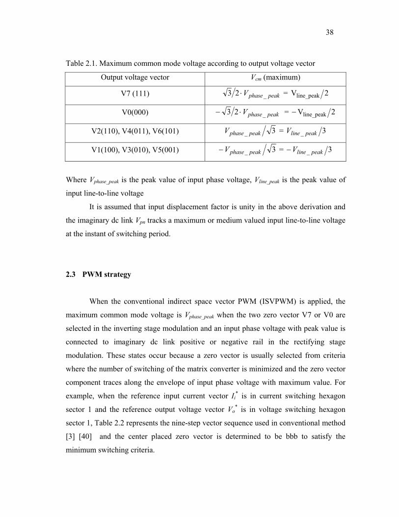
38
Table 2.1. Maximum common mode voltage according to output voltage vector
Output voltage vector Vcm (maximum)
V7 (111) peakphaseV _23 ⋅ = 2Vline_peak
V0(000) peakphaseV _23 ⋅− = 2Vline_peak−
V2(110), V4(011), V6(101) 3_ peakphaseV = 3_ peaklineV
V1(100), V3(010), V5(001) 3_ peakphaseV− = 3_ peaklineV−
Where Vphase_peak is the peak value of input phase voltage, Vline_peak is the peak value of
input line-to-line voltage
It is assumed that input displacement factor is unity in the above derivation and
the imaginary dc link Vpn tracks a maximum or medium valued input line-to-line voltage
at the instant of switching period.
2.3 PWM strategy
When the conventional indirect space vector PWM (ISVPWM) is applied, the
maximum common mode voltage is Vphase_peak when the two zero vector V7 or V0 are
selected in the inverting stage modulation and an input phase voltage with peak value is
connected to imaginary dc link positive or negative rail in the rectifying stage
modulation. These states occur because a zero vector is usually selected from criteria
where the number of switching of the matrix converter is minimized and the zero vector
component traces along the envelope of input phase voltage with maximum value. For
example, when the reference input current vector Ii* is in current switching hexagon
sector 1 and the reference output voltage vector Vo* is in voltage switching hexagon
sector 1, Table 2.2 represents the nine-step vector sequence used in conventional method
[3] [40] and the center placed zero vector is determined to be bbb to satisfy the
minimum switching criteria.

39
Table 2.2 Nine step vector sequence (current hexagon : 1 , voltage hexagon : 1)
γβ γα δα δβ 0 δβ δα γα γβ
aac acc bcc bbc bbb bbc bcc acc aac
Fig. 2.2 (a) shows the phase voltage component of zero vector under the
optimized ISV-PWM [40] with unity displacement power factor and shows the
magnitude of phase voltage component ranges from 0 to 23 of Vphase_peak. Since the
matrix converter is able to use 3 different kinds of zero vectors such as aaa, bbb and ccc,
a proper selection of zero vector leads to the decrease in the common mode voltage
magnitude. If a phase voltage with medium value within an input current switching
hexagon sector is chosen as a zero vector, the maximum magnitude of common mode
voltage is reduced to 21 Vphase_peak from 23 Vphase_peak and Fig. 2.2 (b) shows the input
phase voltage component of zero vector under the proposed ISV-PWM. In other words,
0π/2
3π/2π ωt
Va Vb Vc
(a)
0
π/2
3π/2π ωt
Va Vb Vc
(b)
Fig. 2.2 Zero vector component (a) the optimized ISVPWM (b) the proposed ISVPWM

40
zero vector aaa is used instead of bbb when the value of phase b is greater than phase a.
But the switching numbers within a sampling period and total switching losses increase
under the above method. Therefore, a proper zero vector placement is required according
to which input phase voltage is chosen as a zero vector component and the following
guidelines are derived to satisfy both common mode voltage reduction and minimum
number of switching.
The input phase voltage with the medium value is chosen as a zero vector
component. (represented in Fig. 4 (a) and (b) with arrows)
The position of zero vector depends on Rθ , the angle of the reference current space
vector Ii*within the actual hexagon sector.
When 60 πθ ≤≤ R , the zero vector is placed on the center.
When 36 πθπ ≤≤ R , the zero vector is placed on the both sides.
When the sum of the input and output hexagon sectors is even, the output vector
sequence must be βααβ
When the sum of the input and output hexagon sectors is odd, the output vector
sequence must be αββα
The input vector sequence is γδ
Table 2.3 shows the vector sequence of the proposed ISVPWM under the above
7 rules. Moreover, since the square rms of ripple current in three phase load depends on
the placement of the zero vector in a sampling period [41] and the proposed method
Table 2.3. Vector sequence of the proposed ISVPWM
condition Switching sequence
Even, 60 πθ ≤≤ R γβ γα δα δβ 0 δβ δα γα γβ
Even, 36 πθπ ≤≤ R 0 γβ γα δα δβ δα γα γβ 0
Odd, 60 πθ ≤≤ R γα γβ δβ δα 0 δα δβ γβ γα
Odd, 36 πθπ ≤≤ R 0 γα γβ δβ δα δβ γβ γα 0

41
distributes zero vector equally within a sampling period, it does not increase ripple
components of input/output current.
2.4 Harmonic performance
In this section, harmonic performance of the proposed PWM strategy is analyzed
by calculating harmonic flux of the output voltage and harmonic charge of the input
current. The both harmonic components are compared with the conventional PWM
strategy.
2.4.1 Output voltage
Fig.2.3 The per-carrier cycle rms value of the harmonic flux

42
To evaluate the output voltage quality of the proposed modulation strategy, the harmonic
flux λh on a per-carrier cycle is usually employed [42]. The harmonic flux in the Nth
carrier cycle is calculated by :
dtVVS
S
TN
NT Okh )()1( *∫
+−=λ (2.5)
In (2.5), Vk is the output voltage vector of the kth state and it changes according to the
selected switching sequence. To compare the performance characterization between the
proposed ISV-PWM and optimized ISV-PWM, the per-carrier harmonic flux error λh is
normalized to the product of the peak value of input phase voltage and half of the
switching period as below:
hpeakphaseS
n VTλλ
−⋅⋅=
34 (2.6)
The normalized per-carrier cycle rms value of the harmonic flux λnRMS2 can be
calculated by
ddnnRMS ∫=1
022 λλ (2.7)
Fig. 2.4 The harmonic flux as a function of the modulation index (solid line : proposed
PWM, dashed line : optimized PWM )

43
Fig. 2.3 show the per-carrier cycle rms value of the harmonic flux as a function
of the input current angle θR and output voltage angle θI for the proposed ISV-PWM.
The contours are plotted for modulation index M of 0.95. Evaluating the waveform
quality and harmonic losses, the per fundamental cycle rms value λnfRMS2 is obtained by
integrating over the entire surface as below:
IRnnfRMS d θθλπ
λπ π
∫ ∫=2
022
022
41 (2.8)
Fig. 2.4 shows the per fundamental cycle rms value λnfRMS2 as a function of the
modulation index M where M is 2/√3·mv. The proposed modulation strategy shows
worse harmonic performance in the entire linear modulation range and the mean value of
harmonic flux increases by 6% compared to the optimized ISV-PWM. It should be noted
that input displacement power factor is unity in the above evaluation.
2.4.2 Input current
Likewise the output voltage harmonic component derivation, the error between
the desired input current and the chosen current space vector result in a high frequency
harmonic input current. The evaluation of the input current quality uses the same idea
and procedure for the output voltage case [42] but the concept of harmonic charge q = I·t
(current-time product) is employed instead of harmonic flux λ = V·t (voltage-time
product) [43]. The harmonic charge qh in the Nth carrier cycle is calculated by:
dtIIq S
S
TN
NT ikh )()1( *∫
+−= (2.9)
In (2.9), Ik is the matrix converter input current vector of the kth state and the magnitude
of the per-carrier harmonic charge is a function of the input current angle θR, output
voltage angle θI, the modulation index M and the output power factor pf. the per-carrier
harmonic charge error qh is normalized to the product of the peak value of output current
and half of the switching period as below

44
Fig.2.5 The per-carrier cycle rms value of the harmonic charge
hpeakoutputS
n qIT
q−⋅⋅
=3
4 (2.10)
The normalized per-carrier cycle rms value of the harmonic charge qnRMS2 can be
calculated by
ddqq nnRMS ∫=1
022 (2.11)
Fig. 2.5 show the per-carrier cycle rms value of the harmonic charge as a
function of the input current angle θR and output voltage angle θI for the proposed ISV-
PWM. The contours are plotted for modulation index M of 0.95 and output power factor
pf of 0.9. Evaluating the waveform quality and harmonic losses, the per-fundamental
cycle rms value qnfRMS2 is obtained by integrating over the entire surface as below:
IRnnfRMS dqq θθπ
π π∫ ∫=
2
022
022
41 (2.12)
Fig. 2.6 and Fig. 2.7 show the per fundamental cycle rms value qnfRMS2 as a
function of the modulation index with output power factor 0.9 and 0.6, respectively. The

45
Fig. 2.6 The harmonic charge as a function of the modulation index under output power
factor=0.9 ( solid line : proposed PWM, dashed line : optimized PWM )
Fig. 2.7 The harmonic charge as a function of the modulation index under output power
factor=0.6 ( solid line : proposed PWM, dashed line : optimized PWM )

46
proposed strategy shows better input harmonic performance and the mean value of
harmonic charge is reduced by 2% and 10% for output power factor 0.9 and 0.6,
respectively. It can be seen the distortion of input current is dependent on the output
power factor.
2.5 Simulation results
(a)
(b)
Fig. 2.8 waveform of Vcm with fout = 50Hz, mV = 0.83 (a) the conventional ISVPWM (b)
the proposed ISVPWM

47
(a)
(b)
Fig. 2.9 waveform of Vcm with fout = 20Hz , mV = 0.33 (a) the conventional ISVPWM
(b) the proposed ISVPWM
To illustrate the advantages obtained by the proposed ISV-PWM, the system of
Fig. 2.1 (a) has been simulated with three phase balanced R-L load (42 Ω, 10 mH) and
208V, 60 Hz utility. Fig. 2.8 (a) shows Vcm when the conventional ISV-PWM is used
with fout = 50Hz, mV = 0.83 and the peak value of Vcm reaches 147 V corresponding to
23 Vphase_peak by zero vector operation. Fig. 2.8 (b) shows Vcm when the proposed ISV-
PWM is used with same condition and the peak value of Vcm decreases to 98 V

48
corresponding to 31 Vphase_peak by active vector operation because the peak value of Vcm
by zero vector is limited to 21 Vphase_peak from 23 Vphase_peak as presented in Fig. 2.2 (a)
and (b). The reducing effect of common mode voltage leads to the reduction of the
induced motor shaft voltage and possible degradation to its bearings [35]. Fig. 2.9 (a)
and (b) show Vcm under fout = 20Hz, mV =0.33 with the conventional ISV-PWM and with
the proposed ISV-PWM, respectively and the Vcm decreases by 34 % regardless of
modulation index mV and output frequency fout of matrix converter.
2.6 Experimental results
To validate the theoretical analysis and simulation, a 230V, 3kVA matrix
converter prototype (Fig. 2.11) was developed. Fig. 2.10 shows the block diagram of the
matrix converter. The prototype consists of a DSP board using TMS320LF2407, a
FPGA board and Analog board for 4 step commutation and several functional digital
logics programmed in Altera EPM7128S, a Gate driver & 6 isolated power supply board
M
InputLC Filter
FM35R12KE3 DSPBoard
FPGA&
AnalogBoard
GateDriverBoard
208 V60 Hz
Utility Input
Fig. 2.10 Block diagram of 3 kVA matrix converter

49
Fig. 2.11 3 kVA laboratory prototype matrix converter
and a power board containing Eupec IGBT Matrix module (FM35R12KE3), voltage and
current sensors and snubbers.
In the experiment, 208V, 2 HP general purpose induction machine is operated
with constant voltage-frequency ratio and switching frequency is 2 kHz. For comparison
of the conventional ISV-PWM and the proposed ISV-PWM, the waveforms of the
common mode voltage Vcm are presented and repeated with various motor speeds in Fig.
2.12 (motor speed = 400 rpm) and Fig. 2.13 (motor speed = 1000 rpm). As shown in Fig.
2.12 (a) and 2.13 (a), there exists the common mode voltage pulses whose magnitude is
23 Vphase_peak when the conventional ISV-PWM is applied. The proposed method
makes the common mode voltage pulse whose magnitude is 23 Vphase_peak be
eliminated, restricting the common mode voltage pulse within a level of 31 Vphase_peak,
as presented in Fig. 2.12 (b) and 2.13 (b) regardless of motor speed. The occurrence and
duration of common mode voltage whose magnitude is 23 Vphase_peak become larger as
motor speed decreases, so the proposed method has greater common mode voltage

50
(a)
(b)
Fig. 2.12 Waveforms with fout = 50Hz , mV = 0.83 (a) the conventional ISVPWM (b)
the proposed ISVPWM (ch 3:VAB and ch 4: Vcm)

51
(a)
(b)
Fig. 2.13 Waveforms with fout = 20Hz , mV = 0.33 (a) the conventional ISVPWM (b)
the proposed ISVPWM (ch 3:VAB and ch 4: Vcm)

52
(a)
(b)
Fig. 2.14 Harmonic spectrum of Vcm with fout = 50Hz , mV = 0.83 (a) the conventional
ISVPWM (b) the proposed ISVPWM
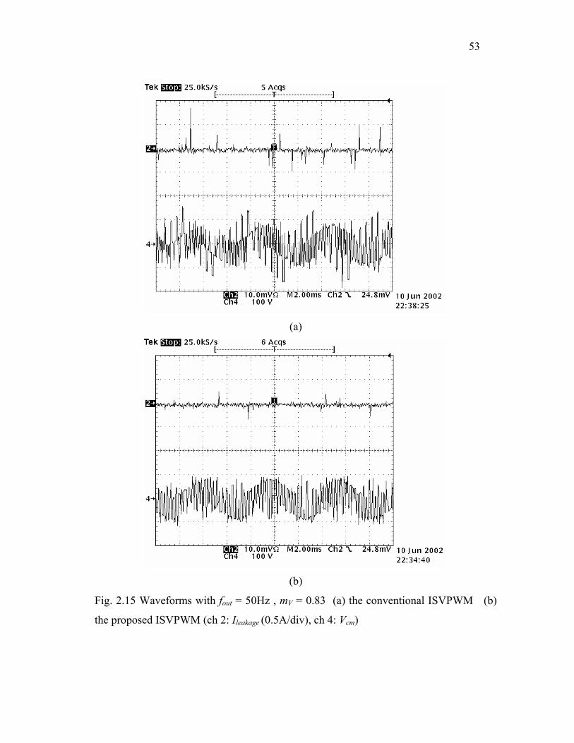
53
(a)
(b)
Fig. 2.15 Waveforms with fout = 50Hz , mV = 0.83 (a) the conventional ISVPWM (b)
the proposed ISVPWM (ch 2: Ileakage (0.5A/div), ch 4: Vcm)

54
reducing effect in the low speed region like Fig. 2.13 (b). Fig. 2.14 (a) and (b) show
harmonic spectrum of Vcm for fout = 50Hz, mV = 0.83 with the conventional ISV-PWM and
the proposed ISV-PWM. The proposed method shows better harmonic spectrum for Vcm
0
20
40
60
80
100
120
140
160
180
200
10 20 30 40 50 60
Output Frequency [Hz]
peak
com
mon
mod
e vo
ltage
[V]
(a)
0
10
20
30
40
50
60
70
80
90
100
10 20 30 40 50 60
Output Frequency [Hz]
RMS
com
mon
mod
e vo
ltage
[V]
(b)
Fig. 2.16 Vcm comparisons of conventional PWM and proposed PWM (a) peak value
(b) rms value
Conventional
Conventional
Proposed
Proposed

55
than the conventional method by decreasing the magnitude of common mode voltage.
Fig. 2.15 (a) and (b) show the leakage current Icm of the motor with conventional ISV-
PWM and proposed ISV-PWM respectively, under fout = 50Hz, mV = 0.83. The peak
value and RMS value are reduced by 17% and 13% when the proposed ISV-PWM is
applied.
Fig. 2.16 (a) and (b) shows the comparison in peak and rms value of common
mode voltage Vcm for various output frequency, respectively. The proposed method
achieves the Vcm reducing effect as much as about 50V in peak value regardless of output
frequency compared to conventional ISV-PWM. A comparison of the rms value of Vcm
shows the Vcm reduction of the proposed method varies according to output frequency
from 11% at 60 Hz and 42% at 10 Hz and it has greater rms common mode voltage
reducing effect in the lower output frequency range due to the required longer zero
vector interval at that range.
2.7 Conclusion
In this chapter, a new modulation strategy for matrix converter has been
proposed. The proposed method has eliminated the common mode voltage components
corresponding to maximum-valued input phase voltage and reduced the magnitude of
peak common mode voltage by 34%. It has been accomplished by choosing a medium-
valued phase voltage as a zero vector component and placing the zero vector in the
center or on the both sides of sampling period. Also the voltage transfer ratio has been
shown to be unaffected by the proposed scheme. Furthermore, the harmonic content of
the input current has been reduced by 2% ~ 10 % and switching losses at the instant of
zero vector transition has been decreased by 5%. However, the conventional scheme has
shown better performance regarding the harmonic contents of output voltage and
harmonic flux of the proposed scheme has been increased by 6%. Finally, experimental
results have been shown to verify the theoretical analysis and simulation.

56
CHAPTER III
RIDE-THROUGH CAPABILITY FOR INPUT VOLTAGE DISTURBANCE*
3.1 Introduction
As discussed in Chapter I, section 1.3, the matrix converter is an array of
controlled bidirectional semiconductor switcehs and the input voltage source is directly
connected to thr output load without any intermediate energy storage elements. It results
the matrix converters are more sensitive to input power disturbances than a conventional
PWM voltage source inverters due to the absence of dc-link.
With the rapid increase of adjustable speed drives (ASDs) in commercial and
industrial facilities, the susceptibility of ASDs under power disturbances such as sags,
swells, transients and short term power interruption (STPI) has become more important
issue. According to a recent survey results, STPI for 0.5 ~ 5 sec and voltage sags of 10
% ~ 40 % below normal grid voltage for 3 ~ 30 cycles are the majority of power
disturbances caused to costly industry process disruption [44]. Although several studies
concerning ride-through capability under power disturbances have been proposed [44]
[45] [46], these studies have focused on three phase PWM rectifier and/or PWM
inverter. Reference [27] proposes an approach for matrix converter with limited ride-
through capability. However, this approach has limitation to develop torque or motor
flux during ride-through interval and needs speed and flux angle observers to re-energize
the motor in the grid condition re-establishment.
This chapter proposes a new ride-through approach for matrix converter fed
ASDs under STPI. In the proposed approach, the topology of a conventional matrix
* 2002 IEEE. Reprinted with permission from “A new ride-through approach for matrix converter fed adjustable speed drives” by H. Cha and P. Enjeti, Conference Record of IEEE Industry Applications Society Annual Meeting, vol. 4, 2002, pp. 2555 – 2560.

57
converter is modified with the addition of three IGBTs and a dc-link capacitor. During a
power interruption, the input grid is disconnected from the ASD by the selective turn-off
of six (out of nine) bidirectional switches. It is shown that the three remaining
bidirectional switches along with the additional IGBTs and dc-link capacitor, a PWM
voltage source inverter (VSI) can be realized. The PWM VSI is then suitably controlled
to maintain rotor flux and guarantee continuous operation of the ASD. Upon restoration
of input grid, the control is simultaneously transferred to the matrix converter mode. The
proposed strategy provides ride-through capability for matrix converter fed ASD and has
the following advantages:
It maintains rotor flux magnitude and keeps synchronization between matrix
converter and motor during STPI.
It allows matrix converter to re-accelerate the motor to the reference speed without
experiencing current transients when normal grid condition is re-established
It operates as an embedded PWM voltage source inverter with dc-link during STPI
and uses space vector PWM to regenerate mechanical energy in the load inertia to
electrical energy in the dc-link capacitor.
Minimum addition of hardware and software is required to the conventional matrix
converter structure.
Simulation and experimental results are shown to demonstrate the advantages of the
proposed approach.
3.2 Ride-through system in matrix converter
In this section, the proposed ride-through system is introduced and its operation
is explained under a short term power interruption. The whole system is divided into two
power modules together with each operating mode according to input voltage condition.
Two operating modes are detailed and control scheme for an uniterrupted mode changes
is designed.

58
3.2.1 Ride-through system configuration
Fig. 3.1 shows the proposed ride-through system for matrix converter. This
system consists of two parts. The first part is a conventional matrix converter module
which operates under normal grid condition, operating for normal mode. The second part
is an add-on ride-through module which extends the matrix converter function to include
the ride-through capability under an abrupt power interruption, operating for ride-
through mode. The three additional IGBTs (SiA, SiB, SiC) together with six IGBTs
(SaA+, SaA-, SaB+, SaB-, SaC+, SaC-) and dc-link capacitor Cdc form a conventional
standard voltage source inverter (VSI) and thereby can use the well-known space vector
PWM method using the same voltage hexagon shown in Fig. 1.8. With three IGBTs
SaA-, SaB- and SaC- fully turning on, each IGBT pair SaA+ and SiA, SaB+ and SiB, and
SaC+ and SiC configures phase A, B, C half-bridge arm of the VSI, respectively. In
other words, the assembly of the above nine IGBTs and dc-link capacitor Cdc results in
M
A
B
C
a
b
c
SaA-
ScC-
SbC-
SaC-
ScB-
SbB-
SaB-
ScA-
SbA-
SiC
SiA
SiBVdc
Cdc
Auxiliaryride-through
module
Matrix converter SaA+
SbA+
ScA+
SaB+
SbB+
ScB+
SaC+
SbC+
ScC+
Fig. 3.1 Matrix converter with ride-through module (SiA, SiB, SiC are add-on IGBTs)

59
an embedded PWM VSI without rectifying diode block. Since the ride-through module
mainly handles magnetizing current component during very short regenerating interval,
current rating of the added three IGBTs and capacitor Cdc can be designed much smaller
than main matrix converter power rating. The Cdc is charging to the rated dc-link voltage
Vdc* which is the peak value of input line-to-line voltage during the normal mode, or
recharged to the Vdc* when the converter returns to the normal mode from the ride-
through mode. The capacitor is charged through the anti-paralleled diodes of three
IGBTs (SiA, SiB, SiC) and input line-to-line voltage Vab or Vac (when Vab > 0 or Vac > 0).
3.2.2 Ride-through strategy
The proposed approach has two operating modes, which are normal mode during
healthy power condition and ride-through mode during power outage. The operation of
both modes is explained together with its working power circuit part and new control
scheme is introduced for smooth transition between two modes.
A. Normal mode
The bold lines in Fig. 3-2 (a) represent the working circuit parts while power grid
condition is healthy and this part is nothing but the matrix converter. Indirect space
vector modulation, which is explained in the operating principle section, generates PWM
patterns for nine bidirectional switches, eighteen IGBTs, in this normal mode. Upon
detecting of an input power failure, the control is simultaneously transferred to the ride-
through mode.

60
M
SaA
ScCSbCSaC
ScBSbBSaB
ScASbA
SiC
SiASiB
(a)
M
SaA
ScCSbCSaC
ScBSbBSaB
ScASbA
SiC
SiASiB
(b)
Fig. 3.2 Operating mode (a) normal mode (b) ride-through mode
B. Ride-through mode
The bold lines in Fig. 3.2 (b) represent the working circuit parts while the input
power is interrupted. During the power interruption, the input grid is disconnected from
the matrix converter by the selective turn-off of six (out of nine) bidirectional switches.
It is shown that the three remaining bidirectional switch set connected in input phase a
along with the additional IGBTs and dc-link capacitor, a PWM voltage source inverter

61
can be realized. It operates as an embedded PWM voltage source inverter with small dc-
link and uses space vector PWM [47] to regenerate mechanical energy stored in the load
inertia into electrical energy in the dc-link capacitor. During this ride-through mode, the
dc-link voltage is maintained at the preset value which is 10% bigger than the rated dc-
link voltage Vdc* and DSP controller maintains rotor flux and keeps synchronization
between matrix converter and motor to guarantee continuous operation of the ASD
regardless of power variation. Upon restoration of input grid, the control is
simultaneously transferred back to the normal mode.
C. Control scheme for both modes
PI controller is employed to ride-through a power outage by regenerating load
inertia. The PI controller regulates the dc-link voltage with acceptable tolerance during
the power interruption by changing the stator reference frequency. Fig. 3.3 shows the
control block diagram for the proposed control scheme. Suppose a power outage occurs
abruptly when the matrix converter runs at normal mode and DSP controller detects it.
At the instant to acknowledge the power loss, the control is transferred to ride-through
mode and PI controller output ωr is in initial value, zero. Thus, the ωr begin to decrease
from zero to negative value as soon as the PI controller is enabled because dc-link
capacitor supplies necessary power instead of input grid and thereby actual dc-link
voltage Vdc begins to collapse rapidly. This negative-going ωr is added to stator reference
frequency ωs and results in stator ride-through frequency ωo. The stator reference
voltage Vo and phase angle θo is calculated by the V/f ratio and transferred to the space
vector PWM (SVPWM) block which calculates PWM patterns for six IGBT gate signals
of the embedded PWM VSI [40]. During the ride-through interval, the converter
supplies almost zero electromechanical torque to the motor and regenerate only a minor
amount of power corresponding to the entire electrical losses in the converter. When the
normal grid condition is re-established and DSP controller detects it, control is

62
Vdc*
Vdc
PI
ωs
ωrV/f
1S
ωo SVPWM
ISVPWMV/f Gate
Driver
Vi
STPIsignal
Vo
Vo
θo
18
6
Normal modeRide-through mode
Fig. 3.3 Control block diagram for the ride-through strategy
transferred to the indirect space vector PWM (ISVPWM) block and re-accelerates motor
shaft speed to the stator reference frequency ωs from the stator ride-through frequency
ωo without any discontinuity in the motor states. Thus the both modes are changed
without experiencing current transients. The ISVPWM block calculates PWM patterns
for eighteen IGBT gate signals of matrix converter and feedbacks input voltage vector Vi
to synchronize with the input grid.
3.3 Simulation results
To illustrate the advantages obtained by the proposed ride-through approach, the
matrix converter of Fig. 3.1 has been simulated in PSIM. The parameters of the
induction motor used in the simulation are P=3HP, UN=208V, fN=60Hz, nN=1710rpm,
J=0.089kgm2, IN=5.8A, TN=11.9Nm, RS=0.435Ω, RR=0.816Ω, LS=LR=2mH,
LM=69.3mH and other simulation conditions are as follows:
Input grid : 208V, 60 Hz
Output frequency : 40 Hz
Switching frequency : 5 kHz
Dc-link capacitor Cdc : 100 µF
Acceleration ramp : 120 Hz/sec
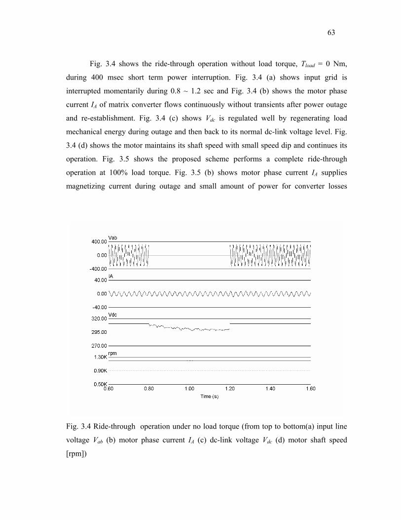
63
Fig. 3.4 shows the ride-through operation without load torque, Tload = 0 Nm,
during 400 msec short term power interruption. Fig. 3.4 (a) shows input grid is
interrupted momentarily during 0.8 ~ 1.2 sec and Fig. 3.4 (b) shows the motor phase
current IA of matrix converter flows continuously without transients after power outage
and re-establishment. Fig. 3.4 (c) shows Vdc is regulated well by regenerating load
mechanical energy during outage and then back to its normal dc-link voltage level. Fig.
3.4 (d) shows the motor maintains its shaft speed with small speed dip and continues its
operation. Fig. 3.5 shows the proposed scheme performs a complete ride-through
operation at 100% load torque. Fig. 3.5 (b) shows motor phase current IA supplies
magnetizing current during outage and small amount of power for converter losses
Fig. 3.4 Ride-through operation under no load torque (from top to bottom(a) input line
voltage Vab (b) motor phase current IA (c) dc-link voltage Vdc (d) motor shaft speed
[rpm])

64
Fig. 3.5 Ride-through operation under 100% load torque (from top to bottom (a) input
line voltage Vab (b) motor phase current IA (c) dc-link voltage Vdc (d) motor shaft speed
[rpm])
regardless of the required load torque during normal mode. Fig. 3.5 (c) shows Vdc is
regulated at 90 % of the predetermined dc-link voltage Vdc* under 100% load torque.
Fig. 3.5 (d) shows motor shaft speed decreases to 50% of reference speed by the
difference between zero electromagnetic torque and 100% load torque during STPI and
re-accelerates toward the reference speed with the acceleration ramp of 120Hz/sec after
input grid re- establishment. It shows the possible duration of the ride-through operation
depends on load torque, initial motor shaft speed and load inertia.

65
3.4 Experimental results
3.4.1 Hardware implementation
A 230V, 3kVA matrix converter prototype (Fig. 3.7) has been built to verify the
proposed approach. The converter is controlled using the indirect space vector
modulation specialized to reduce common mode voltage [17]. Fig. 3.6 shows block
diagram of the matrix converter with ride-through module. The completer control system
is implemented on TMS320LF2407 DSP board. FPGA and analog board contains Altera
FPGA EPM7128S for 4 step commutation, analog signal conditioning and protection
circuits. IGBT Matrix module (FM35R12KE3) and three discrete IGBTs
(IRG4PH50KD) for embedded PWM VSI, voltage, current sensors and snubber circuits
are mounted on power board.
M
InputLC Filter
FM35R12KE3 DSPBoard
FPGA&
AnalogBoard
GateDriverBoard
230 V60 Hz
Utility Input
ridethroughmodule
Fig. 3.6 Block diagram of 3kVA matrix converter with ride-through module

66
Ride-through3 IGBTs
Ride-throughdc capacitor
Gate driver &Power supply
DSP board
Current Sensors
Voltage sensors
FPGA &Analog board
Fig. 3.7 3 kVA matrix converter with ride-through module
3.4.2 Results using the ride-through module
The matrix converter with ride-through module operates with output frequency
of 40 Hz and switching frequency of 5 kHz into a 208V, 2HP induction motor and
programmable AC power source (California Instruments) is used to emulate a three-
phase grid with disturbances. A separate functional test for matrix converter and ride-
through module has been carried out. Fig. 3.8 shows the output current IA and output
line-to-line voltage VAB when matrix converter module is running at 30 Hz. It is seen the
matrix converter supplies sinusoidal output current with low harmonic contents and the
output line-to-line voltage reflects 360 Hz peak envelope of input source voltage. The

67
Fig 3.8 Matrix converter module operation. (ch2 : input voltage Vab, ch3: output current
IA [5A/div], ch4: output line-to-line voltage VAB )
Fig 3.9 Ride-through module operation (ch2 : input voltage Vab, ch3: output current IA
[5A/div], ch4: output line-to-line voltage VAB )

68
add-on ride-through module has been tested with the same load and input condition with
extra B6 type rectifier to verify its feasibility. Fig. 3.9 shows the output current IA and
output line-to-line voltage VAB running at 30 Hz and 300V dc link voltage is provided by
extra B6 rectifier.
Fig. 3.10 (a), (b) and (c) show the output line-to-line voltage VAB (Ch.2), input
line-to-line voltage Vab (Ch. 3), output current IA (Ch. 4, [5A/div]) and STPI detect signal
(Ch. 1, 0: normal mode, 1: ride-through mode). Fig. 3.10 (a) shows the waveforms while
the input grid is healthy, i.e. normal mode and the proposed system works as a matrix
converter at fixed output frequency 40 Hz. The matrix converter supplies sinusoidal
output current with low harmonic contents corresponding to load torque and the rippled
PWM pulse train of VAB tracks 360 Hz peak envelope of input grid voltage which is a
typical waveform of matrix converter. Fig. 3.10 (b) shows the waveforms while the input
grid is interrupted, i.e. ride-through mode. The proposed system regenerates the
mechanical energy from the motor by decreasing a motor speed. The ride-through
module works as a voltage source inverter and controls the motor all the time of this
mode. Therefore output current IA flows continuously even though the input voltages
disappear but decreases to the magnetizing current level of the motor. The flat peak
value of PWM pulse train of VAB represents the dc-link voltage is well regulated by the
PI controller. In the above two figures, STPI signal denotes the present operating mode
and is calculated by real time STPI detection algorithm programmed on DSP. The “1” of
STPI signal indicates momentary power interruption occurs (Fig. 3.10 (b)) and the STPI
signal is “0” during normal grid condition (Fig. 3.10 (a)). An experiment about mode
change between normal mode and ride-through mode has been done. Fig. 3.10 (c) shows
waveforms at transition moment from ride-through mode to normal mode when input
grid is reestablished after momentary power interruption. The output line-to-line voltage
VAB changes from the typical waveform of PWM VSI to the typical waveform of matrix
converter without any pulse dropping. The output current IA flows continuously without
transients and its magnitude returns from magnetizing current level back to magnitude

69
(c)(a) (b)
Ride-thru modeNormal mode Normal modeRide-thru modeNormal mode Normal mode
(a) (b) (c)
1
2
4
3
Fig. 3.10 Waveforms at power disturbance (a) normal mode (b) ride-through mode (c)
mode transition from ride-through mode to normal mode (ch1: STPI, ch2: output line-to-
line voltage VAB, ch3 : input voltage Vab, ch4: output current IA [5A/div])
corresponding to load torque. Fig. 3.11 compares the matrix converter without ride-
through module (Fig. 3.11 (a)) and with the module (Fig. 3.11 (b)) when the input grid is
interrupted and then re-established. Fig. 3.11 (a) shows matrix converter without the
module is comparatively sensitive to an input voltage disturbance and tripped by over
current at the instant of power outage. Meanwhile, matrix converter with the module
ride-though the momentary power interruption effectively and output current IA flows
continuously without any transients between mode changes caused by power outage and
re-establishment as shown in Fig. 3.11 (b).

70
(a)
(b)
Fig. 3.11 Comparison during power interruption (a) without ride-through module (b)
with ride-through module (ch1: STPI, ch2: output current IA [5A/div]), ch3: input
voltage Vab, ch4: output line-to-line voltage VAB)

71
Fig. 3.12 Mode changes between normal mode and ride-through mode (ch1: STPI
detector signal (0: normal mode, 1: ride-through mode), ch2: output frequency fOUT, ch3:
input voltage Vab, ch4: output current IA )
Fig. 3.12 shows the proposed ride-through operation when the input grid is
interrupted for 500 msec and then reestablished. Programmable AC power source
(California Instruments) has been used to emulate a three-phase grid with disturbances.
While the STPI detector signal is ‘1’, ride-through module and PI controller decrease
output frequency fOUT from reference frequency 40 Hz to 25 Hz and it regulates dc-link
voltage to 275 V by regenerative operation. After power recovery, it reaccelerates the
motor up to the reference frequency 40 Hz and the STPI detector signal go back to ‘0’.
Output current IA flows continuously without any transients between mode changes
caused by power outage and re-establishment.

72
3.5 Alternative scheme
Fig. 3.13 shows an alternative scheme to achieve ride-through capability in the
matrix converter. In this article, the topology of conventional matrix converter is
modified to add a small dc-link capacitor and then realize the embedded PWM VSI,
which runs in regenerative operation during power outage. However, matrix converter
usually employs dc capacitor for a voltage clamp circuit, which is needed to absorb the
energy trapped in the leakage inductances of motor and protect switching devices against
voltage spikes when an abrupt shutdown occurs. The voltage clamp circuit consists of
clamp capacitor and two B6-type diode bridges connected to input and output phases of
bidirectional switches. Therefore, another embedded PWM VSI can be simply realized
by replacing the output side B6 diode bridge by six IGBTs which configures three-phase
VSI as illustrated in Fig. 3.13. The dc capacitor is shared as a snubber clamp capacitor in
the normal mode and a dc-link in the ride-through mode. Current rating of six IGBTs are
selected much smaller than the main matrix converter power rating due to the same
reason as the added ride-through module case.
M
SaA
ScCSbCSaC
ScBSbBSaB
ScASbA
Voltage clamp & ride-through
Fig. 3.13 Modified voltage clamp circuit for ride-through capability

73
3.6 Conclusion
In this chapter, a new ride-through approach for matrix converter has been
proposed. The proposed approach has been shown to maintain the rotor flux and keep
synchronization between the motor and matrix converter during momentary power
interruption. It has been shown that by regenerating the mechanical energy stored in load
inertia and transferring it to dc-link capacitor within the embedded PWM VSI part,
successful ride-through operation is accomplished. Further, the matrix converter has
been shown to re-accelerate the motor to the reference speed without any current
transients when normal grid power is restored. The duration of the ride-through
operation depends on initial motor shaft speed level, load torque type and load inertia
and so the approach is more effective for applications with sufficient load inertia. The
ride-through capability has been achieved by the minimal addition of hardware and
software into the matrix converter.

74
CHAPTER IV
HIGH-FREQUENCY LINK TO INCREASE VOLTAGE TRANSFER RATIO*
4.1 Introduction
Distributed generation and storage technologies are an ever increasing portion of
the electric supply resources and most of these new energy technologies produce output
voltage and frequency that are incompatible with the existing utility. Therefore, static
power converters should be integrated with these technologies to provide the necessary
compatibility. When we consider a variable-speed constant-frequency application such
as microturbine and wind turbine, a typical candidate for power converters is an
AC/DC/AC PWM converter/inverter. In some cases, these applications request the
flexible voltage step-up/down transformation to meet the standard utility voltages such
as 230V, 380V and 480V and electrical galvanic isolation between variable speed source
and utility for safety consideration. Conventional VSCF systems employ an AC to DC
converter, dc-link, DC to AC inverter followed by a line frequency isolation transformer.
This approach suffers from bulky 60 Hz magnetic components and large dc-link
electrolytic capacitors.
Since the power throughput density in the transformer is proportional to the
operating frequency, increasing the frequency allows higher utilization of the magnetic
core and reduction in transformer size. A solid-state transformer employing a high
frequency ac link stage was proposed to reduce power transformer volume [48].
Although several studies adopting high-frequency link has been proposed, these studies
have focused on DC/AC conversion [49] for UPS application and AC/DC conversion
* 2003 IEEE. Reprinted with permission from “A three-phase AC/AC high-frequency link matrix converter for VSCF applications” by H. Cha and P. Enjeti, IEEE Power Electronics Specialist Conference 2003, vol. 4, 2003, pp. 1971 – 1976.

75
with zero-voltage switching [50] for high power rectifier. An application of high
frequency link to direct AC/AC conversion has not been presented in the literature.
This chapter proposes a new three-phase AC/AC high-frequency link matrix
converter. In this approach, the variable speed three-phase ac source is chopped to 50 %
duty square wave pulses by the proposed PWM scheme and transferred through single-
phase high frequency transformer and finally established as a fixed frequency utility
voltage. The dc-link reactive energy components are eliminated along with a related
initial charging circuit. The advantages of the proposed approach are:
1. Flexible voltage transfer ratio to meet the several standard utility voltages
2. Electrical galvanic isolation between variable-speed source and fixed frequency
utility source
3. Full utilization of input voltage for dc-link stage and near symmetric square wave
pulse trains to the high-frequency transformer regardless of the operating frequency
of variable speed input source
4. High power density due to minimization of magnetic components and bulky dc link
capacitors
5. Controllable displacement power factor at output utility
6. Bi-directional power flow capability which is able to start up microturbine as a motor
load and then operate it as a generator
7. lower total harmonic distortion of the input and output currents
Simulation and experimental results are shown to demonstrate the advantages of the
proposed approach.

76
4.2 High-frequency link matrix converter
4.2.1 Proposed topology
Fig. 4.1 (a) shows the circuit diagram of the proposed high frequency link matrix
converter topology and it has two power conversion stages, i.e., the variable speed
source 3φ/1φ matrix converter part (primary side converter) for balanced three-phase
variable-frequency ac to high frequency ac (HFAC) and the utility interactive 1φ/3φ
matrix converter part (secondary side converter) for HFAC to fixed-frequency utility ac,
respectively. A small and efficient high-frequency (HF) transformer is placed between
the two power conversion stages and the HFAC with a form of 50% duty square wave
pulse is transferred through it to provide input/ output isolation and required voltage
transfer ratio. Each of twelve bidirectional switches is constructed by connecting two
IGBTs in back-to-back shown in Fig. 4.1 (b).
In this paper, the utility interactive 1φ/3φ matrix converter is modified from using
six bidirectional switches (Fig. 4.1) to ten IGBT switches with unfiltered dc-link block
Utility line
ABC
a
bc
Vp Vs
3φ/1φ Converter 1φ/3φ ConverterHF Transformer
Variable speedSource
(a) (b)
Fig. 4.1 (a) proposed 3φ/3φ high frequency link matrix converter (b) bidirectional
switch configuration
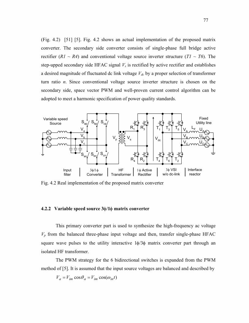
77
(Fig. 4.2) [51] [5]. Fig. 4.2 shows an actual implementation of the proposed matrix
converter. The secondary side converter consists of single-phase full bridge active
rectifier (R1 ~ R4) and conventional voltage source inverter structure (T1 ~ T6). The
step-upped secondary side HFAC signal Vs is rectified by active rectifier and establishes
a desired magnitude of fluctuated dc link voltage Vdc by a proper selection of transformer
turn ratio n. Since conventional voltage source inverter structure is chosen on the
secondary side, space vector PWM and well-proven current control algorithm can be
adopted to meet a harmonic specification of power quality standards.
Vp Vs
3φ/1φ Converter
HFTransformer
Variable speedSource
FixedUtility line
Vdc
Sap Sbp Scp
San SbnScn
R1
R2
R3
R4
T1
T6
T5
T4
T3
T2
VA
VB
VC
UA
UB
UC
LFVa
Vb
Vc
1φ ActiveRectifier
3φ VSIw/o dc-link
Interfacereactor
Inputfilter
Fig. 4.2 Real implementation of the proposed matrix converter
4.2.2 Variable speed source 3φ/1φ matrix converter
This primary converter part is used to synthesize the high-frequency ac voltage
Vp from the balanced three-phase input voltage and then, transfer single-phase HFAC
square wave pulses to the utility interactive 1φ/3φ matrix converter part through an
isolated HF transformer.
The PWM strategy for the 6 bidirectional switches is expanded from the PWM
method of [5]. It is assumed that the input source voltages are balanced and described by
)cos(cos tVVV inimaima ωθ ==

78
)32cos(cos πωθ −== inimbimb VVV (4.1)
)32cos(cos πωθ +== inimcimc VVV
where ωin is the input angular frequency and is changeable according to an operating
point of distributed generating system. Within any 60° interval between two successive
zero crossings of input phase voltages, shown in Fig. 4.3, only one of the three-phase
input voltages has the maximum absolute value and the other phase voltages have
opposite polarity voltage. For example, in the mode 1 , phase a has the maximum
positive value and phase b and c have negative values in Fig. 4.3 and |||||| cba VVV +=
0 π/2 π ωιt
Va Vb Vc
1 2 3 465 5
-π/2
Fig. 4.3 Six modes of input phase voltages
Under mode 1 and positive pulse mode at Vp, switch Sap remains turned on and switch
Sbn, Scn are modulated within one switching period TS while all other switches remain
turned off. In order to satisfy unity displacement power factored input current
requirement and full utilization of input source voltage, the duty ratio db, dc of switch Sbn
and Scn are given by
|cos||cos|
a
bbd
θθ
= , |cos||cos|
a
ccd
θθ
= (4.2)
From Fig. 4.2 and Fig. 4.4(c), the output dc link voltage Vdc is
))()(( cacbabdc VVdVVdnV −+−= (4.3)
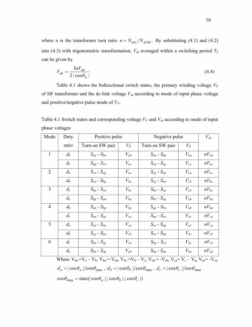
79
where n is the transformer turn ratio primNNn sec= . By substituting (4.1) and (4.2)
into (4.3) with trigonometric transformation, Vdc averaged within a switching period TS
can be given by
|cos|23
a
imdc
nVV
θ= (4.4)
Table 4.1 shows the bidirectional switch states, the primary winding voltage VP
of HF transformer and the dc-link voltage Vdc according to mode of input phase voltage
and positive/negative pulse mode of VP.
Table 4.1 Switch states and corresponding voltage VP and Vdc according to mode of input
phase voltages
Positive pulse Negative pulse Mode Duty
ratio Turn-on SW pair VP Turn-on SW pair VP
Vdc
db Sap - Sbn Vab San - Sbp Vba nVab 1
dc Sap - Scn Vac San - Scp Vca nVac
da Scn - Sap Vac Scp - San Vca nVac 2
db Scn - Sbp Vbc Scp - Sbn Vcb nVbc
dc Sbp - Scn Vbc Sbn - Scp Vcb nVbc 3
da Sbp - San Vba Sbn - Sap Vab nVba
db San - Sbp Vba Sap - Sbn Vab nVba 4
dc San - Scp Vca Sap - Scn Vac nVca
da Scp - San Vca Scn - Sap Vac nVca 5
db Scp - Sbn Vcb Scn - Sbp Vbc nVcb
dc Sbn - Scp Vcb Sbp - Scn Vbc nVcb 6
da Sbn - Sap Vab Sbp - San Vba nVab
Where Vab =Va – Vb, Vba =-Vab, Vbc =Vb – Vc, Vcb = -Vcb, Vca= Vc – Va, Vac= -Vca
maxcos|cos| θθaad = , maxcos|cos| θθbbd = , maxcos|cos| θθccd =
|)cos||,cos||,cosmax(|cos max cba θθθθ =

80
Fig. 4.4 (a) ~ (c) show the high frequency link operating mechanism at mode 1,
with excessively increased switching period TS so that resulted square wave pulses can
be observed in detail. In this example, two square-wave pulses are applied to the primary
winding of HF transformer in each mode (Fig. 4.4 (b). At the beginning of every
switching interval TS, duty db of Vab is used. Bidirectional switch Sap and Sbn are turned
on creating a positive pulse Vab across the primary winding and a current pulse is
flowing from phase a into phase b during db⋅TS . At the end of the same switching
interval TS, duty dc of Vac is used. Bidirectional switch Sap and Scn are turned on creating
Mode 1
(a)
(b)
Va
Vb
Vc
VabVac
VcaVba
dbTS dbTS dbTS dbTSdcTS dcTS dcTS dcTS
ωt
ωt
Positive pulse Positive pulseNegaitivepulse
Negaitivepulse
(c)
Vdc
ωt
Fig. 4.4 PWM pattern generation (a) duty cycle in input phase voltage (b) 50% duty
square wave in the primary voltage VP (c) fluctuated dc-link voltage Vdc

81
a positive pulse Vac across primary winding and a current pulse is flowing from phase a
into phase c during dc⋅TS . In order to keep the HF transformer flux balanced, a negative
voltage pulse is applied across the primary winding in the next switching period.
Bidirectional switch San and Sbp are turned on generating negative pulse Vba during db⋅TS
and then San and Scp are turned on generating negative pulse Vca during dc⋅TS . In the
consecutive switching cycle, the above positive and negative pulse train with 50% duty
and different magnitude is repeated as shown in Fig. 4.4 (b). The pulse train VP is
stepped up/down to VS through HF transformer and then VS is rectified to a fluctuated dc-
link voltage Vdc as shown in Fig. 4.4 (c).
Since the frequency range of variable speed source varies widely, synchronous or
asynchronous PWM is chosen depending on the operating variable speed source
frequency in the primary side converter control. It is chosen according to the frequency
modulation ratio defined by
in
priswf f
fm _= (4.5)
where fin is the varying variable speed source frequency and fsw_pri is the switching
frequency of primary side converter. For small value of mf, the phases of primary
converter and variable speed source should be synchronized to each other for full
utilization of available input voltage and improvement of input current waveform
quality. Also, mf should be a multiple of six because the whole range of input phase is
divided into six modes. By changing switching frequency fsw_pri to be multiples of six of
the input frequency, it distributes the square wave pulse train to be quarter-wave
symmetric about the each center of modes and guarantees the magnetizing flux balance
at the HF transformer. Meanwhile, the average voltage loss of Vdc due to asynchronous
PWM is small at the larger value of mf and the asynchronous PWM can be used where
the frequency of primary converter is kept constant, whereas the frequency of input
voltage varies, resulting in non-integer values of mf.
82
4.2.3 Utility interactive 1φ/3φ matrix converter
The secondary converter part is similar to the traditional AC/DC/AC converter
system without DC capacitors [51]. IGBT switches R1, R2, R3 and R4 are controlled to
rectify 50% duty square wave VS into fluctuated dc-link voltage Vdc and active switches
are used for bidirectional power flow instead of B4-type diode rectifier. When secondary
voltage of HF transformer is positive pulse (VS > 0) , R1 and R2 are turned on and R3
and R4 are turned-on at negative pulse (VS < 0) to maintain Vdc positive. In practical
implementation, resistor – capacitor – diode snubber circuit is adopted to mitigate the
effect of leakage inductance of HF transformer and circuit layout and the snubber energy
is regenerated to input side or output side by using the IGBT switches. It should be
noticed that four active switches can be replaced by four diodes when out power factor is
more than 0.87 and bidirectional power flow is no longer required.
Conventional voltage source inverter structure (T1 ~ T6) is used as the power
stage from fluctuated dc-link to fixed frequency utility and two methods are used to
satisfy low current distortion and unity displacement factor. First, the synchronous
reference-frame d and q current regulators are adopted with the feed-forward
compensation of speed voltage term to eliminate the cross coupling between the d and q
phases [52] and it allows the reduction of the current control loops to first-order plants
and improved their tracking capability. Second, cosθmax in Table 1 is multiplied to the
final PWM voltage command of the above current controller to compensated highly
fluctuated dc-link voltage and distribute its pulse within the pulse width generated by
primary converter in average level.
4.2.4 HF transformer design consideration
This part deals with the proper selection of dc-link voltage, takes into account the
utility voltage fluctuation and the reduced voltage transfer gain in primary side converter

83
and derives a minimum turn-ratio n of HF transformer to accommodate these issues. The
secondary side converter with well-designed current controller and fixed frequency
utility can be modeled as two independent ac voltage sources connected through
inductor LF, which acts as the load between utility voltage U and converter output
voltage V shown in Fig. 4.5 (a). The direction of power flow between these two sources
depends on their magnitudes (Um and Vom) and phase angles ( θU and θV). The voltage
and current relationships of the utility interactive 1φ/3φ matrix converter can be analyzed
using the phasor diagram in Fig. 4.5 (b). Neglecting the resistor drop in the line and
assuming unity displacement factor operation (synchronous frame reactive current Ide =
0), the amplitude of the converter output voltage Vom can be calculated as
22 )( eqFomom ILUV ω+= (4.6)
where fo utility frequency
ωo 2π fo
Iqe active component current
In order to avoid saturation in a space vector pulse width modulator and considering a
maximum modulation index of 0.95, the peak phase voltage Vom must be
95.03
⋅≤ dcom
VV where
23 im
dcnV
V = (4.7)
Combining (4.6) and (4.7), the boundary condition for PWM saturation can be given as a
relationship between dc-link voltage Vdc and utility voltage Um and a required turn-ratio
n of HF transformer is derived as
95.03
)(2 22
⋅
+≥=
im
eqFom
p
s
V
ILU
NN
nω
(4.8)
The primary purpose of HF transformer is to reduce the size, weight and volume
and to improve efficiency. In order to achieve this, a standard grain-oriented silicon-steel

84
jωLF
Vom θv Um θu
Iqe
Iqe
UmVom
jωLF Iqe
(a) (b)
Fig. 4.5 (a) equivalent circuit model (b) phasor diagram when displacement factor is 1.0
core transformer is chosen and an operating frequency of 1.2 kHz to 2.4 kHz is used [18]
for the verification of the proposed approach. However, amorphous core material and
coaxial windings are required for real 96,000 rpm rotating microturbine application [24].
4.3 Simulation results
To illustrate the advantages obtained by the proposed high frequency link matrix
converter, the system of Fig. 2 has been simulated with the following conditions:
Input variable speed source : 208V, 30 Hz
Output utility : 208V, 60 Hz
HF transformer turn ratio n : 1:1.3
Utility interface inductor : 1.5 mH
fSW in 3φ/1φ matrix converter part : 2 kHz
fSW in 1φ/3φ matrix converter part : 10 kHz
Fig. 4.6 shows input phase voltage Va at 30 Hz, input phase current Ia before
passing through input LCR filter, primary winding voltage Vp and primary current Ip of

85
Fig. 4.6 Primary side 3φ/1φ matrix converter waveforms (fin = 30 Hz)
Fig. 4.7 Secondary side 1φ/3φ matrix converter waveforms (fout = 60 Hz)

86
HF transformer. The primary part 3φ/1φ matrix converter draws only active component
of current Ia with unity displacement factor and tracks the phase of variable speed of
distributed power generator. The waveform of Ia illustrates low total harmonic distortion
and it means the design of the high speed generator into a given volume is simplified
considerably [53].
The waveform of primary current Ip represents the proposed flux balancing
method works as desired. Fig. 4.7 shows utility phase voltage VA at 60 Hz, output current
IA through utility interactive inductor LF, secondary winding voltage Vs of HF
transformer and fluctuated dc-link voltage Vdc . The secondary side 1φ/3φ matrix
converter supplies only active component of current IA with unity displacement factor.
The waveform of IA illustrates very low total harmonic distortion of the output current
and it satisfies the requirements of power quality standard.
4.4 Experimental results
To validate the proposed topology and PWM pattern generation, a 230V, 3kVA
high frequency link matrix converter prototype was developed. In order to evaluate
asynchronous PWM mode at larger value of mf, 208V, 60Hz utility is applied to the
primary side and the secondary side is connected to 170V, 60 Hz utility step-downed by
variable auto-transformer. Fig. 4.8 shows the primary winding voltage Vp, input line
voltage Vab, fluctuated dc-link voltage Vdc where mf = 33.3 is used. The reestablished dc-
link voltage waveform represents asynchronous PWM works as desired. Fig. 4.9 shows
unfiltered input current Ia and input phase voltage Va. Ia is in phase with Va. Fig. 4.10
illustrates input current Ia, fluctuated dc-link voltage Vdc, output phase voltage VA and
output current IA. Since the same utility is used at both input and output side, Ia and IA
are in phase with output phase voltage VA and it shows unity power factor operation is
occurred at both sides. Fig. .4.11 show the harmonic spectrum of unfiltered input current

87
Fig.4.8 High frequency link waveforms at 60Hz input (ch2: Vp, ch3: Vab, ch4: Vdc )
Fig.4.9 Primary side waveforms at 60Hz input (ch2: Ia (10A/div), ch3: Va )

88
Fig.4.10 Input/out waveforms at 60Hz input (ch1: IA (20A/div), ch2: Ia (20A/div), ch3:
VA, ch4: Vdc )
Fig. 4.11 FFT results at 60Hz input (ch M1: Ia, ch M2: IA )

89
Fig. 4.12 High frequency link waveforms at 400Hz input (ch1: mode, ch2: Vp, ch3: Vab,
ch4: Vdc )
Fig. 4.13 Input/out waveforms at 400Hz (ch1: IA (20A/div), ch2: Ia (20A/div), ch3: VA,
ch4: Va )

90
Ia and output current IA. Although the input current waveform is contaminated by
switching frequency, FFT result shows it contains fundamental component and 9%, 6%
of 5th and 7th harmonics, respectively because secondary converter distribute its pulse
within the pulse width generated by primary converter in average mode, not
instantaneous mode. However the output current FFT result shows only fundamental
components. It should be noticed the lower order harmonics can be eliminated if primary
side and secondary side pulses are correlated based on traditional matrix converter [3]
but it requests complex calculation and considerable hardware burden.
For the check of synchronous PWM at small value of mf, 140V, 400 Hz generator
output is applied to the primary side and 127V, 60Hz to the secondary side. Fig. 4.12
shows mode generated by primary side converter, input line voltage Vab, primary
winding voltage Vp and fluctuated dc-link voltage Vdc when mf is 6. The square wave
pulse are symmetric each other and one pulse is generated at each mode due to
successful synchronization. Fig. 4.13 illustrates input/ output phase voltage and current,
respectively. Although output current is near sinusoidal and keep unity power factor,
input current is same as rectifier current loaded by continuous current source because
primary side converter acts like uncontrolled rectifier at mf = 6. Therefore, larger value
of mf is required to improve input current waveform quality depending on an application.
4.5 Conclusion
In this chapter, a new three phase AC/AC high-frequency link matrix converter
has been proposed. The proposed matrix converter has been shown to maintain unity
displacement factor and low harmonic distortion in both variable speed source and
utility. The added HF transformer into the intermediate stage of dual-bridge matrix
converter has provided electrical galvanic isolation and flexible voltage transfer ratio,
which makes it possible to be connected with any commercial utility voltage. Further,
the proposed system has been shown to maintain the characteristics of a conventional
matrix converter: with bidirectional power flow, no dc-link capacitors, improved

91
reliability and availability. The above advantages have made the proposed topology to be
a competitive solution for VSCF distributed generation system such as wind-turbine and
micro-turbine. The feasibility of the proposed high frequency link matrix converter has
been verified through simulation and experiments.

92
CHAPTER V
SOFT SWITCHING DC/AC DIRECT CONVERTER
5.1 Introduction
Fuel cells are electrochemical devices that convert hydrogen and oxygen directly
into electricity and water. Although they are emerging as a viable clean energy source
for static power generation as well as moving vehicles [54], this source produces widely
varying low dc voltage which is incompatible with the existing utility and shows slow
dynamic response for sudden load change. To accommodate the low dc voltage of fuel
cells (42 ~ 60V) to the required split 120V/240V single phase ac voltage, a typical fuel
cell based power conditioner has two parts; variable low dc -to- fixed high dc converter
and dc/ac converter, and battery/ ultra capacitor is utilized to improve load dynamics
[55]. Although several power circuit topologies have been proposed in the literature,
these approaches are focused on the improvement of dc/dc converter part [56][57][58] or
inverter part [59], separately. A research for a complementary operation of dc/dc
converter and inverter has not been presented in the literature.
This paper proposes a new soft switching direct converter for residential use and
new PWM scheme is proposed to synchronize both dc/dc converter and inverter
switching instants. Inverter operating condition for zero current commutation and zero
voltage switching requirements in the dc/dc converter are analyzed and clamp circuit
deign is discussed. The advantages of the proposed direct converter are:
Switching losses in dc/dc converter are nearly zero due to the combined ZVS and
ZCS operation
ZVS occurs throughout the whole load range since ZVS in dc/dc converter uses
magnetizing current of transformer
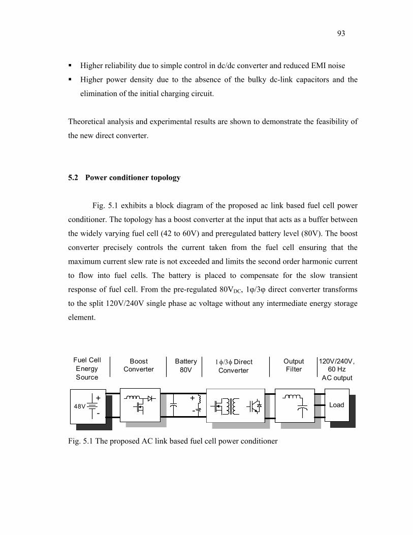
93
Higher reliability due to simple control in dc/dc converter and reduced EMI noise
Higher power density due to the absence of the bulky dc-link capacitors and the
elimination of the initial charging circuit.
Theoretical analysis and experimental results are shown to demonstrate the feasibility of
the new direct converter.
5.2 Power conditioner topology
Fig. 5.1 exhibits a block diagram of the proposed ac link based fuel cell power
conditioner. The topology has a boost converter at the input that acts as a buffer between
the widely varying fuel cell (42 to 60V) and preregulated battery level (80V). The boost
converter precisely controls the current taken from the fuel cell ensuring that the
maximum current slew rate is not exceeded and limits the second order harmonic current
to flow into fuel cells. The battery is placed to compensate for the slow transient
response of fuel cell. From the pre-regulated 80VDC, 1φ/3φ direct converter transforms
to the split 120V/240V single phase ac voltage without any intermediate energy storage
element.
Load
Fuel CellEnergySource
+-
+
-48V
BoostConverter
1φ/3φ DirectConverter
Battery80V
OutputFilter
120V/240V,60 Hz
AC output
Fig. 5.1 The proposed AC link based fuel cell power conditioner

94
VS
DC-linkless3φ Inverter
Vdc
R1
R2
R3
R4
T1
T6
T5
T4
T3
T2
VA
VN
VB
LF CF
VP
Split120/240V60 Hz AC
LC FilterSoft switchingdc/dc converter
Preregulated80VDC
S1 S3
S4 S2
Clampcircuit
IP IS
VC
IC
U
V
W
VIN
IDC
Fig. 5.2 The proposed 1φ/3φ direct converter for resident power system
Fig. 5.2 illustrates the proposed 1φ/3φ direct converter. It consists of soft
switching dc/dc converter, dc-linkless 3φ inverter and output LC filter. The soft
switching dc/dc converter is divided into primary dc/dc converter, high frequency
transformer, secondary synchronous rectifier and clamp circuit. The primary dc/dc
converter generates 20 kHz square wave from the preregulated 84VDC and steps up to
420VDC through high frequency transformer and synchronous rectifier. Further, the
preregulated 84VDC leads to a full utilization of magnetic material and simple open loop
control for square wave generation. The parasitic (or added) capacitors across MOSFET
and clamp circuit allow ZVS (Zero Voltage Switching) turn-on and ZCS (Zero Current
Switching) turn-off, respectively, whose operations are introduced in section 5.4. The
secondary synchronous rectifier is used to reduce conduction loss and provide
bidirectional power flow path when load displacement power factor is less than 0.866
[5].
The proposed inverter is the same as the three phase inverter without dc link
capacitor [51][60]. The inverter supplies split 120V/240V single phase ac output directly
without bulky dc link electrolytic capacitors, which results in lower power profile and
improved reliability. A new PWM scheme provides zero vector interval for the inverter
while dc/dc converter switches are commutating at zero current and its principle is
introduced in section 5.3.

95
VS
DC-linkless3φ Inverter
Vdc
R1
R2
R3
R4
T1
T6
T5
T4
T3
T2
LF
VP
3φ, 220V60 Hz AC
Interfacereactor
Soft switchingdc/dc converter
Preregulated80VDC
S1 S3
S4 S2
ClampCircuit
UA
UB
UC
Fig. 5.3 The proposed 1φ/3φ direct converter for 3φ utility interface
It should be noticed that the proposed direct converter for resident use can be
applied in 3φ 220 VAC utility interface mode just by removing output filter capacitors
and employing conventional space vector modulation together with synchronous frame
PI current controller [60]. Fig. 5.3 exhibits 1φ/3φ direct converter for 3φ utility interface
and synchronous rectifier can be replaced by full bridge diode rectifier when the direct
converter supplies unity power factored current to utility.
5.3 PWM strategy in inverter stage
The proposed inverter employs the conventional 3φ voltage source inverter
topology and it means a standard 6-pack IGBT module can be used to generate split
120/240V single phase ac voltage. IGBT T1, T4 arm, T3, T6 arm and T5, T2 arm
produce VA, VN and VB, respectively and their reference voltages are defined as follows,
VA-REF = ma·sin (2π·60·t) (5.1)
VN-REF = 0 (5.2)
VB-REF = -ma·sin (2π·60·t) (5.3)
Where ma is modulation index

96
Phase A reference voltage VA-REF is 180º out of phase with Phase B reference
voltage VB-REF. Phase N reference voltage VN-REF is always zero and generates 50%
square wave gate signal VN-GATE as shown in Fig. 5.4 (b). The average value of square
wave VN is zero and provides virtual ground over VA, VB. Fig. 4 shows an example of
the proposed PWM scheme when VA-REF is in positive peak (θ = 90º ) and thereby VB-REF
is in negative peak. When output voltage vector is defined as a sequence of [VA VN VB],
possible voltage vectors are divided into two active vector [100], [110] and two zero
vectors [000], [111].
VA-REF
VN-REF
VB-REF
000 100 110 111 110 100 000
VA- gate
VN-gate
VB-gate
VSSquarwave
Voltagevector
VAN
VBN0
0
VDC
VDC
0-VDC
VDC
(a)
(b)
(c)
(d)
TS
Fig. 5.4 PWM patterns at θ = 90º and zero vector position

97
Both zero vectors are placed in both ends and center of each switching period TS
as shown in Fig. 4 (b). During the zero vector intervals, output currents freewheel
through upper switches or lower switches in case of [111] or [000], respectively and the
dc/dc converter switches are commutating as shown in Fig. 5.4 (d). It means inverter dc
link current IDC and dc/dc converter secondary current IS are all equal to zero in this
interval. Therefore, the primary current IP is reduced to magnetizing current IM and
commutates at near zero current. Fig. 5.4 (c) exhibits the resulted PWM patterns in
output VAN and output VBN.
Modulation index of 0.85 is assumed to provide enough zero vector interval for
ZCS and ZVS switching in the dc/dc converter. It is worth to note that three leg iron core
type 3φ reactor can be employed owing to the above PWM scheme.
5.4 Soft switching strategy in dc/dc converter
Primary dc/dc converter operates as simple square wave generator and uses
magnetizing current for ZVS turn on at every switching transition. Therefore ZVS
operation occurs independent of the magnitude of load current and voltage surges are
nearly eliminated at switching instants [61].
Also, the switching instants of dc/dc converter are synchronized with the zero
vector interval of inverter. The synchronization leads to ZCS turn off at the dc/dc
converter switches and elimination of reverse recovery phenomenon at secondary
rectifier. Therefore, voltage overshoot and ringing caused from the interaction of the
reverse recovery process of the rectifier with the leakage inductance of the transformer
are almost eliminated. The clamp circuit is placed to support ZCS operation and clamp
voltage surges caused from stray inductances of dc link power layout. Furthermore, the
energy trapped in snubber CS is regenerated to output side through the inverter switches.

98
5.4.1 ZCS turn-off operation
While the primary dc/dc converter is commutating, the voltage vector of inverter
is zero vector (000 or 111) by the aforementioned PWM scheme. This condition
indicates the dc link IDC current becomes zero during the commutation of dc/dc
converter switches and inverter output current freewheels through inverter active
switches and anti-parallel diodes. However, the primary current keeps conducting by the
leakage inductance Llk of transformer. If the energy stored in the leakage inductance can
be eliminated before the dc/dc converter switches commutate, zero current turn-on and -
off at the dc/dc converter is possible and switching losses are significantly reduced. In
other words, the eight switches of primary and secondary dc/dc converter commutate
under discontinuous current mode. Therefore it can eliminate reverse recovery
phenomenon and the pertinent EMI which occurs in continuous current mode of
conventional rectifying diodes.
In order to remove the trapped energy at leakage inductance on time, clamp
circuit is placed in the dc-link as shown in Fig. 5.2. When voltage vector of inverter
changes from active vector (100 or 110) to zero vector (000 or 111), inverter part
becomes separated from the dc/dc converter part. Since the secondary current IS in
leakage inductance is no longer able to conduct to the load through inverter switches, IS
is directed to the clamp circuit and dc link voltage is clamped to snubber capacitor
voltage VC.
Fig. 5.5 shows (a) the equivalent circuit and (b) secondary current IS of the dc/dc
converter during the above interval. In the equivalent circuit, the transformer is
represented by the leakage inductance Llk because magnetizing current freewheels
through primary side path and is not seen in the clamp circuit. The equivalent circuit is
valid until IS discharges to zero.

99
IS IS(0+)
VIN
Llk
CS
DS
VC(0+)IC
IS
Treset
T=0+
(a) (b)
Fig. 5.5 (a) equivalent circuit at ZCS turn-off and (b) IS during inverter zero vectors
From the equivalent circuit, the snubber capacitor current IC and voltage VC are
)sin()0(
)cos()0()(*
tZVV
tItI oo
CINoSC ωω
++ −
+⋅= (5.4)
where Slk
o CL1
=ω S
lko C
LZ =
Llk : leakage inductance referred to secondary side
CS : snubber capacitance
VIN* : preregulated voltage referred to secondary side
VC(0+), IS(0+) : initial value of VC and IS
The magnetic energy stored in leakage inductance is transferred to the electrostatic
energy in snubber capacitor Cs at Treset by resonance and Treset is derived by using IC
(Treset) = 0 at (4)
))0(
(tan*
1
INc
ooSlkreset
VV
IZCLT
−=
+− (5.5)

100
5.4.2 ZVS turn-on operation
In general, ZVS is preferable over ZCS at high switching frequency and the
reason is related with the parasitic capacitances of the switch [2]. Since the secondary
current IS becomes zero before dc/dc converter changes square wave polarity, load
current component is disappeared and magnetizing current component is only considered
in the ZVS turn-on operation. During the switching transition, magnetizing current
provides the constant charging/discharging current to parasitic (or added) capacitance
across eight dc/dc converter MOSFET switches. Therefore transition time is constant
regardless of the load current level because the peak value of magnetizing current is
determined by preregulated voltage level of 80V. In addition, there is no significant
conduction loss penalty to achieve ZVS as in the case of conventional phase shift
modulated converter because ZVS operation is carried out by magnetizing current.
Assuming equivalent parasitic capacitance of each MOSFET and peak
magnetizing current are CP and IM-pk, the resulted charging/discharging time is
pkM
INpZVS I
VCt
−=
4 (5.6)
The blanking time between half bridge switches of dc/dc converter should be chosen
greater than tZVS and zero vector interval of inverter should be greater than the sum of
Treset and the blanking time for smooth ZCS and ZVS operation.
5.4.3 Clamp circuit design consideration
Assuming CS to be large relative to switching period and handled energy, the
snubber capacitor and clamp circuit can be replaced by a dc source VC in steady state.
Since the waveform must repeat from one time period to the next in steady state, the
integral of the charged and discharged energy on snubber capacitor over one period must

101
be zero. Therefore, The charged energy from leakage inductance with switching
frequency fSW
CHRG = SWSlk fIL 221 2 ⋅ (5.7)
is all dissipated at snubber resistor RS in every switching period TS.
Assuming snubber capacitor voltage is VC in steady state and VC is enough for the
desired Treset, the resistor RS is determined by
CHRG
CP
VR
2= (5.8)
5.5 Experimental results
To validate the theoretical analysis, a 230V 3kVA soft switching direct converter
prototype was developed. The controller consists of a DSP board using
TMS320LF2407and interface board including FPGA (Altera EPM7128S) for digital
Fig. 5.6 3kVA direct matrix converter
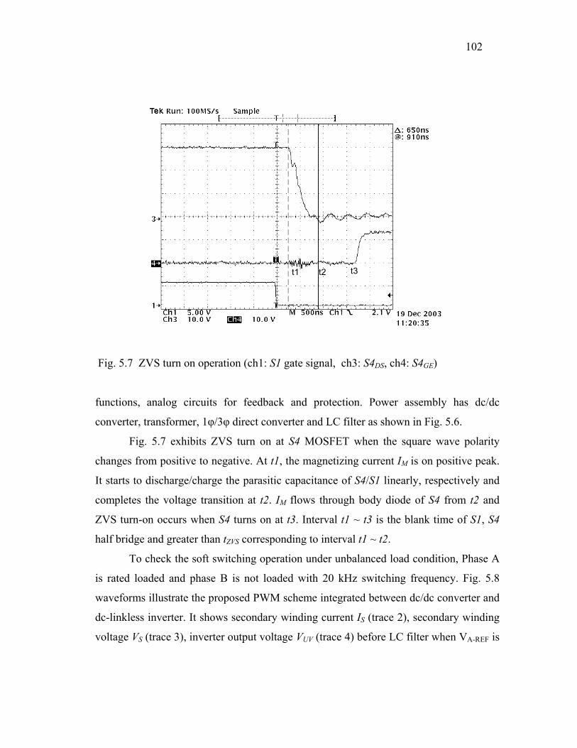
102
t1 t2 t3
Fig. 5.7 ZVS turn on operation (ch1: S1 gate signal, ch3: S4DS, ch4: S4GE)
functions, analog circuits for feedback and protection. Power assembly has dc/dc
converter, transformer, 1φ/3φ direct converter and LC filter as shown in Fig. 5.6.
Fig. 5.7 exhibits ZVS turn on at S4 MOSFET when the square wave polarity
changes from positive to negative. At t1, the magnetizing current IM is on positive peak.
It starts to discharge/charge the parasitic capacitance of S4/S1 linearly, respectively and
completes the voltage transition at t2. IM flows through body diode of S4 from t2 and
ZVS turn-on occurs when S4 turns on at t3. Interval t1 ~ t3 is the blank time of S1, S4
half bridge and greater than tZVS corresponding to interval t1 ~ t2.
To check the soft switching operation under unbalanced load condition, Phase A
is rated loaded and phase B is not loaded with 20 kHz switching frequency. Fig. 5.8
waveforms illustrate the proposed PWM scheme integrated between dc/dc converter and
dc-linkless inverter. It shows secondary winding current IS (trace 2), secondary winding
voltage VS (trace 3), inverter output voltage VUV (trace 4) before LC filter when VA-REF is

103
t1 t2 t3 t4 t5
t6 t7
Fig. 5.8 ZCS operation with θ = 270º, unbalanced load (ch2: Is (5A/div), ch3: Vs, ch4:
VUV)
in negative peak (θ = 270º). At t1, VUV pulse is turned on and begins to supply power to
resistor load through LC filter. At this instant, IS builds up through leakage inductance
Llk until it reaches to output load current at t2 and thereby a voltage dip occurs in the dc-
link voltage VDC which is reflected in VS. At t3, inverter switching status is changed to
zero vector (000) and output load current starts to freewheel through lower switches of
inverter. Meanwhile, IS keeps conducting through transformer leakage inductance and
transfer its trapped magnetic energy to snubber capacitor CS by t4. During t3 ~ t4, VDC is
clamped by snubber capacitor voltage VC and this interval corresponds to Treset at (5.5).
After t4, the primary winding current is reduced to magnetizing current level and is used
for energy source for ZVS at the dc/dc converter. At t5, dc/dc converter changes the
polarity of its square wave and ZVS occurs at four half bridge arms. The interval t5 ~ t6
corresponds to tZVS at (5.6) and blanking time of half bridge arms is chosen greater than
tZVS. Since the dc/dc converter switching occurs at almost zero current and zero voltage,

104
Fig. 5.9 Inverter output voltage under unbalanced load (ch2: IA (10A/div), ch3: VAN, ch4:
VBN )
its switching losses are nearly disappeared and pertinent EMI is drastically reduced. At
t7, VUV pulse turns on again and the same operation is repeated. Therefore, zero vector
interval is t3 ~ t7 and is determined by inverter modulation index. It should be noticed
that output load currents are supplied directly from preregulated 80VDC through
transformer without any intermediate reactive energy reservoir.
Fig. 5.9 shows phase A voltage VAN (trace 3), phase B voltage VBN (trace 4) and
phase A load current IA (trace 2). VAN is out of 180º phase with VBN and has the same
magnitude as VBN even though phase A is loaded by 1kW resistor and phase B is not
loaded. Since the snubber capacitor voltage VC can be initially charged to two times the
normal value by a resonance of Llk and CS, the snubber capacitor CS needs to be
precharged during a start-up period. This precharging can be implemented solely by a
proper design of the control circuit without any additional components. To accomplish
this, all secondary converter switches R1 ~ R4 turn off and thereby synchronous rectifier

105
t1 t2
Fig. 5.10 Snubber capacitor CS initial charge (ch3: VS, ch4: VC)
becomes diode rectifier during the start-up period, t1 ~ t2 in Fig. 5.10. The duty cycle of
primary converter should be increased with some slew rate to obtain the normal dc link
voltage without damaging dc/dc converter switches.
5.6 Conclusion
In this chapter, a new soft switching direct converter has been presented for
residential fuel cell system. The proposed dc/dc converter has been shown high
efficiency & lower EMI due to soft switching through whole load range without
significant conduction loss penalty as in the case of the conventional phase shifted dc/dc
converter. The proposed dc-linkless inverter makes the entire system compact and
increases the system reliability by removing electrolytic capacitors. The synchronized
and complementary PWM strategy between dc/dc converter and inverter has resulted in

106
ZVS and ZCS operation in the square wave switching instants. The operating principle
and design considerations for circuit parameters have been addressed and checked in no
load, balanced load and unbalanced load condition. Finally, preliminary experimental
results have been shown to verify the feasibility of the proposed direct converter.

107
CHAPTER VI
CONCLUSIONS
6.1 Conclusions
This dissertation is primarily concerned with several aspects of matrix converter
design for practical industry applications. Three different types of matrix converter
topologies have been introduced and each prototype has been built to demonstrate the
feasibility of the proposed toplogies and control strategies.
In Chapter I, a brief overview of the matrix converter technolgies and indirect
space vector modulation have been presented. Next, research objectives and dissertation
outlines are clearly delineated.
In Chapter II, a new modulation strategy for matrix converter has been presented
to reduce the common mode voltage. The common mode voltage corresponding to peak
input phase voltage has been eliminated by choosing a medium-valued phase voltage as
a zero vector component and placing the zero vector in the center or on the both sides of
sampling period. Therefore the voltage transfer ratio is unaffected by the modulation
scheme. Further, the harmonic content of the input current is reduced and switching
losses at the instant of zero vector transition are decreased. Finally, experimental results
have been shown to verify the theoretical analysis and simulation.
In Chapter III, a new ride-through module for matrix converter has been
proposed. The proposed module has been shown to maintain the rotor flux and
synchronization between the motor and matrix converter during momentary power
interruption. It has been shown that by regenerating the mechanical energy stored in load
inertia and transferring it to dc-link capacitor within the embedded PWM VSI part,
successful ride-through operation is accomplished. Further, the matrix converter has
been shown to re-accelerate the motor to the reference speed without any current

108
transients when normal power is restored. The ride-through capability has been achieved
by the minimal addition of hardware and software into the matrix converter.
In Chapter IV, a new three phase AC/AC high-frequency link matrix converter
has been proposed. The proposed matrix converter has been shown to maintain unity
displacement factor and low harmonic distortion in both variable speed source and
utility. The added high frequency transformer into the intermediate stage of dual-bridge
matrix converter provides electrical galvanic isolation and flexible voltage transfer ratio,
which makes it possible to be connected with a commercial utility voltage. Further, the
high-frequency link converter has been shown to maintain the characteristics of a
conventional matrix converter: with bidirectional power flow, no dc-link capacitors,
improved reliability and availability. The above advantages make the proposed topology
to be a competitive solution for VSCF distributed generation system such as wind-
turbine and micro-turbine. The feasibility of the proposed high frequency link matrix
converter has been verified through simulation and experiments.
In Chapter V, a new soft switching direct converter has been presented for
residential fuel cell system. The dc/dc converter stage has been shown high efficiency
and lower EMI due to the soft switching through whole load range. The dc-linkless
inverter stage makes the entire system compact and increases the system reliability by
removing bulky electrolytic capacitors. The synchronized and complementary PWM
strategy between dc/dc converter and inverter has resulted in ZVS and ZCS operation.
The operating principle and design considerations for the converter have been addressed.
Finally, experimental results have been shown to verify the feasibility of the direct
converter.
6.2 Suggestions for future work
Continuation of the work in this dissertation could be focus on the unbalanced
input voltage and output load conditions. The three schemes presented in Chapters II to

109
IV are based on balanced input voltages. Further investigation would also be required
during grid disturbance such as voltage sag or swell. Experimental results would be
provided by using 1kVA direct converter along with PEM fuel cell.

110
REFERENCES
[1] L. Gyugyi, and B. R. Pelly, Static Power Frequency Changers: Theory,
Performance, and Application. New York: Wiley, 1976.
[2] N. Mohan, T. M. Undeland, and W. P. Robbins, Power Electronics: Converters,
Applications, and Design. Hoboken, NJ: John Wiley & Sons, 2003.
[3] L. Huber, and D. Borojevic, “Space vector modulated three-phase to three-phase
matrix converter with input power factor correction,” IEEE Trans. on Industry
Applications, vol. 31, pp. 1234-1245, Nov./Dec. 1995.
[4] H. Cha, and P. N. Enjeti, “An approach to reduce common-mode voltage in
matrix converter,” IEEE Trans. on Industry Applications, vol. 39, pp. 1151-1159,
July/August 2003.
[5] L. Wei, and T. A. Lipo, “A novel matrix converter topology with simple
commutation,” in Conf. Rec. IEEE-IAS Annu. Meeting, vol. 3, 2001, pp. 1749-
1754.
[6] P. Nielsen, F. Blaabjerg, and J. K. Pedersen, “Space vector modulated matrix
converter with minimized number of switchings and a feedforward compensation
of input voltage unbalance,” in Proc. IEEE International Conference on Power
Electronics, Drives and Energy Systems for Industrial Growth, vol. 2, 1996, pp.
833 – 839.
[7] M. Hornkamp, M. Loddenkötter, M. Muenzer, O. Simons, and M. Bruckmann,
“Economac, the first all-in-one IGBT module for matrix converters,” in Proc.
Drivers and Controls and Power Electronics Conf., London, U.K, 2001, pp. 35-
39.
[8] S. Bernet, T. Matsuo, and T. A. Lipo, “A matrix converter using reverse blocking
NPN-IGBTs and optimized pulse patterns,” in Proc. IEEE PESC’96, vol. 1,
1996, pp. 107 -113.

111
[9] M. Takei, T. Naito, and K. Ueno, “The reverse blocking IGBT for matrix
converter with ultra-thin wafer technology,” in Proc. IEEE ISPSD’03, 2003, pp.
156 – 159.
[10] N. Burany, “Safe control of four-quadrant switches,” in Conf. Rec. IEEE-IAS
Annu. Meeting, vol. 1, 1989, pp. 1190 – 1194.
[11] L. Zhang, C. Wathanasarn, and W. Shepherd, “Switch sequencer circuit for safe
commutation of a matrix converter,” Electronics Letters, vol. 31, pp. 1530 -
1532, Aug. 1995.
[12] J. Youm, and B. Kwon, “Switching technique for current-controlled AC-to-AC
converters,” IEEE Transactions on Industrial Electronics, vol. 46, pp. 309 –318,
April 1999.
[13] M. Ziegler, and W. Hofmann, “Implementation of a two steps commutated
matrix converter,” in Proc. IEEE PESC’99, vol. 1, 1999, pp. 175 – 180.
[14] P. W. Wheeler, J. C. Clare, L. Empringharn, M. Bland, and M. Apap, “Gate drive
level intelligence and current sensing for matrix converter current commutation,”
IEEE Trans. on Industrial Electronics, vol. 49, pp. 382 –389, April 2002.
[15] J. Mahlein, J. Igney, J. Weigold, M. Braun, and O. Simon, “Matrix converter
commutation strategies with and without explicit input voltage sign
measurement,” IEEE Trans. on Industrial Electronics, vol. 49, pp. 407 –414,
April 2002.
[16] P. Nielsen, “The matrix converter for an induction motor drive,” Doctoral
dissertation, Aalborg University, Aalborg East, Denmark, 1996.
[17] C. L. Neft, and C. D. Schauder, “Theory and design of a 30-hp matrix converter,”
in Conf. Rec. IEEE-IAS Annu. Meeting, vol. 1, 1988, pp. 934 -939.
[18] A. Schuster, “A matrix converter without reactive clamp elements for an
induction motor drive system,” in Proc. IEEE PESC’98, vol. 1, 1998, pp. 714 –
720.
[19] J. Mahlein, and M. Braun, “A matrix converter without diode clamped over-
voltage protection,” in Proc. IEEE PIEMC’00, vol. 2, 2000, pp. 817 – 822.

112
[20] P. N. Enjeti, and X. Wang, “A critical evaluation of harmonic generated by
forced commutated cycloconverters under unbalance,” in Proc. IEEE IECON’90,
vol. 2, 1990, pp. 1162 -1166.
[21] S. Kwak, R. M. O. Dabbousi, and H. A. Toliyat, “An instantaneous
compensation technique for supply disturbances in direct frequency converters,”
in Proc. IEEE IECON’02, vol. 2, 2002, pp. 956 – 960.
[22] D. Casadei, G. Serra, and A. Tani, “Reduction of the input current harmonic
content in matrix converters under input/output unbalance,” IEEE Trans. on
Industrial Electronics, vol. 45, pp. 401 - 411, June 1998.
[23] D. Casadei, G. Serra, and A. Tanl, “A general approach for the analysis of the
input power quality in matrix converters,” in Proc. IEEE PESC’96, vol. 2, 1996,
pp. 1128 -1134.
[24] F. Blaabjerg, D. Casadei, C. Klumpner, and M. Matteini, “Comparison of two
current modulation strategies for matrix converters under unbalanced input
voltage conditions,” IEEE Trans. on Industrial Electronics, vol. 49, pp. 289 -
296, April 2002.
[25] J. Kang, H. Hara, A. M. Hava, E. Yamamoto, E. Watanabe, and T. Kume, “The
matrix converter drive performance under abnormal input voltage conditions,”
IEEE Trans. on Power Electronics, vol. 17, pp. 721 – 730, Sept. 2002.
[26] W. Lixiang, Y. Matsushita, and T. A. Lipo, “Investigation of dual-bridge matrix
converter operating under unbalanced source voltages,” in Proc. IEEE PESC’03,
vol. 3, 2003, pp. 1293 – 1298.
[27] C. Klumpner, I. Boldea, and F. Blaabjerg, “Limited ride-through capabilities for
direct frequency converters,” IEEE Trans. on Power Electronics, vol. 16, pp.
837-845, Nov. 2001.
[28] E. P. Wiechmann, R. P Burgos, and J. Rodriguez, “Continuously motor-
synchronized ride-through capability for matrix-converter adjustable-speed
drives,” IEEE Trans. on Industrial Electronics, vol. 49, pp. 390 –400, April
2002.

113
[29] M. Venturini, “A new sine wave in, sine wave out, conversion technique
eliminates reactive elements”, in Proc. POWERCON 7, 1980, pp. E3_1-E3_15.
[30] M. Venturini, and A. Alesina, “Analysis and design of optimum-amplitude nine-
switch direct AC-AC converters,” IEEE Trans. on Power Electronics, vol. 4, pp.
101 - 112, Jan. 1989.
[31] D. G. Holmes, and T. A. Lipo, “Implementation of a controlled rectifier using
AC-AC matrix converter theory,” in Proc. IEEE PESC’89, vol. 1, 1989, pp. 353
-359.
[32] D. Casadei, G. Grandi, G. Serra, and A. Tani, “Space vector control of matrix
converters with unity input power factor and sinusoidal input/output waveforms,”
in Proc. EPE’93, vol. 7, 1993, pp. 170 – 175.
[33] J. Oyama, X. Xiarong, T. Higuchi, and E. Yamada, “Displacement angle control
of matrix converter,” in Proc. IEEE PESC’97, vol. 2, 1997, pp. 1033 – 1039.
[34] S. Ishii, E. Yamamoto, H. Hara, E. Watanabe, A. M. Hara, and X. Xia, “A vector
controlled high performance matrix converter – induction motor drive,” in Proc.
IPEC’00, Tokyo, Japan, 2000, pp. 235 – 240.
[35] D. A. Rendusara, and P. N. Enjeti, “An improved inverter output filter
configuration reduces common and differential modes dv/dt at the motor
terminals in PWM drive systems,” IEEE Trans. on Power Electronics, vol. 13,
pp. 1135 – 1143, Nov. 1998.
[36] H. Lee, and S. Sul, “A common-mode voltage reduction method modifying the
distribution of zero voltage vector in PWM converter/inverter System,” in Conf.
Rec. IEEE-IAS Annu. Meeting, vol. 3, 1999, pp. 1596-1601.
[37] A. L. Julian, G. Oriti, and T. A. Lipo, “Elimination of common-mode voltage in
three-phase sinusoidal power converters,” IEEE Trans. on Power Electronics,
vol. 14, pp. 982-989, Sep. 1999.
[38] J-K Kang, H. Hara, E. Yamamoto, and E. Watanabe, “Analysis and evaluation of
bidirectional power switch losses for matrix converter drive,” in Conf. Rec.
IEEE-IAS Annu. Meeting, vol. 1, 2002, pp. 438-443.

114
[39] S. Bernet, S. Ponnaluri, and R. Teichmann, “Design and loss comparison of
matrix converters and voltage-source converters for modern AC drives,” IEEE
Trans. on Industrial Electronics, vol. 49, pp. 304-314, April 2002.
[40] P. Nielsen, F. Blaabjerg, and J. K. Pedersen, “Space vector modulated matrix
converter with minimized number of switching and a feedforward compensation
of input voltage unbalance,” in Proc. of PEDES’96, vol. 2, 1996, pp. 833-839.
[41] D. G. Holmes, “The significance of zero space vector placement for carrier-based
PWM schemes,” IEEE Trans. on Industry Applications, vol. 32, pp. 1122-1129,
Sep./Oct. 1996.
[42] A. M. Hava, R. J. Kerkman, and T. A. Lipo, “Simple analytical and graphical
methods for carrier-based PWM-VSI drives,” IEEE Trans. on Power Electronics,
vol. 14, Jan. 1999.
[43] K. B. Larsen, A. H. Jorgensen, L. Helle, and F. Blaabjerg, “Analysis of
symmetrical pulse width modulation strategies for matrix converters,” in Proc.
IEEE PESC’02, vol. 2, 2002, pp. 899-904.
[44] A. V. Jouanne, P. N. Enjeti, and B. Banerjee, “Assessment of ride-through
alternatives for adjustable-speed drives,” IEEE Trans. on Industry Applications,
vol. 35, pp. 908 – 916, July/Aug. 1999.
[45] J. Holtz, W. Lotzkat, and S. Stadtfeld, “Controlled AC drives with ride-through
capability at power interruption,” IEEE Trans. on Industry Applications, vol. 30,
pp. 1275-1283, Sept./Oct. 1994.
[46] Y-S. Kim, and S-K. Sul, “A novel ride-through system for adjustable-speed
drives using common-mode voltage,” IEEE Trans. on Industry Applications, vol.
37, pp. 1373-1382, Sept./Oct. 2001.
[47] H. W. Broeck, H-C Skudelny, and G. V. Stanke, “Analysis and realization of a
pulsewidth modulator based on voltage space vector,” IEEE Trans. on Industry
Applications, vol. 24, pp. 142-150, Jan./Feb. 1988.

115
[48] M. Kang, and P. N. Enjeti, “Analysis and design of electronic transformers for
electric power distribution system,” IEEE Trans. on Power Electronics, vol. 14,
pp. 1133 – 1141, Nov. 1999.
[49] M. Matsui, M. Nagai, M. Mochizuki, and A. Nabae, “High-frequency link
DC/AC converter with suppressed voltage clamp circuits-naturally commutated
phase angle control with self turn-off devices,” IEEE Trans. on Industry
Applications, vol. 32, pp. 293-300, March/April 1996.
[50] V. Vlatkovic, D. Borojevic, and F. C. Lee, “A zero-voltage switched, three-phase
isolated PWM buck rectifier,” IEEE Trans. on Power Electronics, vol. 10, pp.
148-156, March 1995.
[51] S. Kim, S. K. Sul, and T. A. Lipo, “AC/AC power conversion based on matrix
converter topology with unidirectional switches,” IEEE Trans. on Industry
Applications, vol. 36, pp. 139-145, Jan./Feb. 2000.
[52] V. Kaura, and V. Blasko, “Operation of a voltage source converter at increased
utility voltage,” IEEE Trans. on Power Electronics, vol. 12, pp. 132-137, January
1997.
[53] M. Suter, “Active filter for a microturbine,” in Proc. INTERLEC’01, 2001, pp.
162-165.
[54] J. H. Hirschenhofer, D. B. Stauffer, R. R. Engleman, and M. G. Klett, “Fuel cell:
opening new frontiers in power generation,” US Department of Energy,
Morgantown, WV, 1999.
[55] E. Santi, D. Franzoni, A. Monti, D. Patterson, F. Ponti, and N. Barry, “A fuel cell
based domestic uninterruptible power supply,” in Conf. Rec. IEEE-IAS Annu.
Meeting, vol. 3, 2001, pp. 1749-1754.
[56] G. O’Sullivan, “Fuel cell inverters for utility applications,” in Proc. IEEE
PESC’00, vol. 3, 2000, pp. 1191-1194.
[57] R. Ayyanar, and N. Mohan, “Novel soft-switching DC-DC converter with full
ZVS-range and reduced filter requirement – part I: regulated-output,” IEEE
Trans. on Power Electronics, vol. 16, pp. 184-192, March 2001.

116
[58] K. Wang, C. Y. Lin, L. Zhu, D. Qu, F. C. Lee, and J. S. Lai, “Bi-directional DC
to DC converters for fuel cell systems,” in Proc. Power Electronics in
Transportation’98, 1998, pp. 47-51.
[59] R. Gopinath, S. Kim, J. Hahn, S. Campbell, P. N. Enjeti, M. Yeary, and J.
Howze, “Development of a low cost fuel cell inverter system with DSP control,”
in Proc. IEEE PESC’02, vol. 1, 2002, pp. 309-314.
[60] H. Cha, and P. N. Enjeti, “A three-phase AC/AC high-frequency link matrix
converter for VSCF applications,” in Proc. IEEE PESC’03, vol. 4, 2003, pp.
1971-1976.
[61] R. Redl, N. O. Sokal, and L. Balogh, “A novel soft-switching full-bridge DC/DC
converter: analysis, design considerations and experimental results at 1.5kW, 100
kHz,” IEEE Trans. on Power Electronics, vol. 6, pp. 408-418, July 1991.
117
VITA
Han Ju Cha received the B.S degree in electrical engineering from Seoul
National University and the M.S degree from Pohang Institute of Science and
Technology, Korea, in 1988 and 1990, respectively. He will receive the Ph. D degree
from Texas A&M University, in August 2004. From 1990 to 2001, he was with LG
Industrial Systems, Anyang, Korea, where he was engaged in the development of power
electronic converters and high power adjustable speed drives. In September 2001, he
began his doctoral program at Texas A&M University in the area of power electronics.
His research interests are high power converters, ac/dc, dc/ac and ac/ac converter
topologies and their control, medium voltage adjustable speed drives, power
conditioners for distributed power sources such as wind, microturbine and fuel cells. He
can be reached through Dr. P. Enjeti, Power Electronics and Power Quality Laboratory,
Department of Electrical Engineering, Texas A&M University, College Station, Texas
77843.