analysis of semiconductor expenses in medium voltage drives
TRANSCRIPT

Lappeenranta-Lahti University of Technology LUT
School of Energy Systems
Degree Programme in Electrical Engineering
ELEC
Analysis of semiconductor expenses in medium voltage drives
Master’s thesis
Examiners: Professor Olli Pyrhönen
Associate professor Pasi Peltoniemi
Supervisor: D.Sc. (Tech.) Riku Pöllänen Lari Ilonen, 2020
Abstract
Lappeenranta-Lahti University of Technology LUT
School of Energy Systems
Degree Programme in Electrical Engineering
Lari Ilonen
Analysis of semiconductor expenses in medium voltage drives
Master’s thesis
2020
59 pages, 18 figures, 11 tables, 1 attachment
Examiners: Professor Olli Pyrhönen
Associate professor Pasi Peltoniemi
Supervisor: D.Sc. (Tech.) Riku Pöllänen
Keywords: multilevel, topology, converter, inverter, IGBT, medium voltage drive,
semiconductor, cost comparison
In this Master’s thesis, semiconductor expenses in multilevel medium voltage drives was
analysed by comparing cost and reliability of five selected topology cases. This was done
by first studying the IGBT modules and topologies in the medium voltage drives (MVD)
market and examining the market situation and price development of High-Voltage IGBT
modules. Reliability calculations for power modules were also demonstrated. Finally, the
performance of the selected topology cases was simulated with simulation tools provided
by IGBT manufacturers.
The results showed that while multilevel medium voltage drives can produce higher power,
the cost can be multiple times higher compared to low voltage drive. Efficiency was
improved with multilevel design but the increase in the number of components reduced the
reliability notably. Multilevel low voltage structure proved to be a cost-effective solution.
The power was increased and the costs were reduced significantly compared to medium
voltage. This was achieved with marginal decrease in reliability.
Tiivistelmä
Lappeenrannan-Lahden teknillinen yliopisto LUT
School of Energy Systems
Sähkötekniikka
Lari Ilonen
Puolijohdekustannusten analyysi keskijännitekäytöissä
Diplomityö
2020
59 sivua, 18 kuvaa, 11 taulukkoa, 1 liite
Työn tarkastajat: Professori Olli Pyrhönen
Apulaisprofessori Pasi Peltoniemi
Ohjaaja: TkT Riku Pöllänen
Hakusanat: monitaso, topologia, konvertteri, invertteri, IGBT, keskijännitekäyttö,
puolijohde, kustannusvertailu
Tässä diplomityössä tutkittiin puolijohdekustannuksia monitasokeskijännitekäytöissä
vertaamalla viittä valittua pääpiiritopologiaa. Tämä tehtiin tutkimalla IGBT-moduuleja ja
topologioita keskijännitekäyttöjen markkinoilla sekä tarkastelemalla markkinoiden
tilannetta ja keskijännite IGBT-moduulien hintakehitystä. Tehomoduuleille suoritettiin
myös toimintavarmuuslaskelmat. Lopuksi valittujen topologia tapausten suorituskykyä
simuloitiin IGBT-valmistajien omilla simulaatiotyökaluilla.
Tulokset osoittivat, että vaikka monitasoiset keskijännitekäytöt voivat tuottaa suurempaa
tehoa, kustannukset voivat olla useita kertoja suuremmat kuin pienjännitekäytöissä.
Hyötysuhde parani monitasoisella rakenteella, mutta komponenttien lisääntynyt määrä
laski toimintavarmuutta. Monitasoinen pienjännitekäyttö osoittautui kustannustehokkaaksi
vaihtoehdoksi. Teho kasvoi suuresti ja kustannukset olivat merkittävästi pienemmät kuin
keskijännitteellä. Tämä saavutettiin marginaalisella toimintavarmuuden alenemisella.

Acknowledgments
This Master’s thesis has been made as part of Yaskawa commissioned power electronics
study from LUT for developing next-generation power electronics technology. I would like
to thank The Switch for interesting and challenging topic that was educational and
provided motivation for my future career as an electrical engineer.
Special thanks to Olli Pyrhönen, who composed the initial idea, and to Riku Pöllänen, who
crystallized the topic and formulated the methodology for the study. Also, thanks to Pasi
Peltoniemi for the feedback and support. I’m grateful for the support that I got from the
company and the instructors and the educational value of the meetings.
I would also like to thank my family and friends for the constant support during writing
this thesis.

1
1 Contents 1 Introduction .................................................................................................................... 4
1.1 Background ............................................................................................................. 4
1.2 Medium voltage drive applications ......................................................................... 4
1.3 Objectives ................................................................................................................ 5
1.4 Outline of the thesis ................................................................................................ 5
2 Power electronics ............................................................................................................ 6
2.1 IGBT ....................................................................................................................... 6
2.2 Converter ............................................................................................................... 13
2.2.1 2-level VSI ..................................................................................................... 13
2.2.2 3-level Neutral Point Clamped Inverter ......................................................... 18
2.2.3 Cascaded H-Bridge Multilevel Inverter ......................................................... 21
2.2.4 5-level HNPC ................................................................................................. 22
2.3 Reliability .............................................................................................................. 24
2.4 The economic effect of voltage ............................................................................. 27
3 Markets and the future trends ....................................................................................... 31
3.1 Market of semiconductors ..................................................................................... 31
3.1.1 IGBT module manufacturers ......................................................................... 32
3.2 Assessment of the cost evolution of the HV-IGBT modules ................................ 34
3.3 Market of the MVD ............................................................................................... 36
4 Topology comparison ................................................................................................... 41
4.1 Research method ................................................................................................... 41
4.2 Simulation tools .................................................................................................... 44
4.3 Results ................................................................................................................... 46
5 Analysis of the results .................................................................................................. 49
6 Conclusions .................................................................................................................. 51
REFERENCES .................................................................................................................... 52
APPENDIX I ......................................................................................................................... 56

2
LIST OF SYMBOLS AND ABBREVIATIONS
AFE Active Front End
CHB Cascaded H-Bridge
CSI Current Source Inverter
DCB Direct Copper Bond
DFE Diode Front End
FIT Failures In Time
FS Field Stop
FWD Free-Wheeling Diode
IGBT Insulated-Gate Bipolar Transistor
IGCT Integrated Gate-Commutated Thyristor
IHM IGBT High-power Module
IHV IGBT High-Voltage module
LVD Low Voltage Drive
MTBF Mean Time Between Failures
MVD Medium Voltage Drive
NPC Neutral Point Clamped
NPT Non-Punch Through
PT Punch Through
SGCT Symmetric Gate-Commutated Thyristor
SiC Silicon Carbide
SVM Space Vector Modulation
TCO Total Cost of Ownership
THD Total Harmonic Distortion
VSD Variable Speed Drive
VSI Voltage Source Inverter
Ustray Voltage spike
Lσ Stray inductance
di Current derivative
dt Time derivative

3
ma Amplitude modulation index
uref Peak reference voltage
utri Peak triangle voltage
uph Peak phase voltage
UDC DC-link voltage
Ud Output voltage
ULL Line-to-line voltage
Uo Input voltage
T Time period
ω Angular velocity
λ Failure rate
πt Temperature factor
πs Voltage breakdown factor
πE Environmental factor
πq Quality factor
Tj Junction temperature
K Energy activation and Boltzmann constant ratio
Uce_off_state Off-state saturation voltage
Uce_rating Rated saturation voltage
C Price/cost
Q cumulative production
β Learning by doing coefficient
W Width
L Length
n Amount
X Cost per power unit
Y Power per surface area
S Apparent power

4
1 Introduction
1.1 Background
In 2018, IPCC (Intergovernmental Panel on Climate Change) published a special report,
“Global Warming of 1.5 °C”, on the impacts of global warming of 1.5 °C above pre-
industrial levels. The report stated that the global temperature had already risen
approximately by one degree and if the warming continues with current rate, the 1.5-
degree limit will be exceeded by the middle of the century. Exceeding this limit would
cause significant risks for both humans and nature. (Finnish Ministry of the Environment,
2019)
The global trend has now become of getting rid of fossil fuels and reducing the CO2
emissions by increasing renewable energy production and improving energy efficiency in
every field of industry. Electrical drives and power conversion systems are key
components in reaching that goal. Addition to improved efficiency, there has become
major demand for higher power converters. Low voltage drives are reaching their potential
power limits. To produce more power, the natural option is to raise voltage.
The Switch is a Yaskawa owned company that specialises in advanced drive train
technology, producing high power converters and electrical motors and generators. The
company was one of the first to realize the use of full power converters and permanent
magnet generators in wind turbines. Nowadays, the company continues to produce
permanent magnet technology, high power converters and high-speed motors in the
marine, wind and turbo industries.
1.2 Medium voltage drive applications
Medium voltage drives (MVDs) have been generally used in high power applications but
are found as low as 200kW and high as 100MW. Voltages range from over 1000V up to
10kV. There are multiple industries that use MVDs, for example energy production, oil
and gas, water and wastewater, metal, chemical, mining, cement and glass, traction and
marine industries.
In marine, applications range from propulsion to thrusters and auxiliary systems. Oil and
gas industry use MVDs in pumps, blowers and compressors and metal industry utilizes
high power MVDs in rolling mills. These applications are critical part of complex
5
processes and downtimes can lead to huge losses or dangerous situations. As such, MVDs
need to be highly reliable and energy efficient.
1.3 Objectives
The main objective of this thesis is to generate a cost comparison of the semiconductor
cost of the most commonly used topologies in high power converters. The emphasis is on
the multilevel topologies with insulated IGBT modules, with industrial applications in
mind. The differences between the topologies and their effect on the whole converter
structure is studied and reflected to the cost comparison so that further analysing is
possible, and the thesis could make a comprehensive conclusion/assumption of a cost-
effective converter topology.
The second objective is to study available semiconductor components and high-power
converters and their manufacturers. Combined with overview of medium voltage markets,
applications and trends, the aim is to forecast to some degree of what trends can be
expected in the near future and where the markets are going.
1.4 Outline of the thesis
Second chapter of this thesis covers IGBTs and converters in medium voltage drives.
IGBT’s structure, types and packaging are introduced and then, different converter
topologies are presented. The reliability and the affect of the drives voltage on the system
costs are analysed.
Third chapter focuses on the markets of the IGBT and medium voltage converters. The
manufacturers and their product portfolios are presented and analysed. Cost development
of the HV-IGBT modules is also estimated in this chapter.
Next chapter demonstrates the research methods and the used simulation tools and
provides results of simulations and calculations. Results are further analysed in the chapter
five.
Finally, conclusions are established in the chapter 6. Final chapter goes through what was
studied in the thesis, what was discovered, how well the initial goals were achieved and
what further research should be conducted.

6
2 Power electronics
2.1 IGBT
Power electronics are used to process and control the flow of electric energy by supplying
voltages and currents in a form that is optimally suited for user loads (Mohan, et al., 2003).
The power electronic devices that are used for this are called power semiconductors.
The simplest semiconductor device is diode. It consists of p-n junction that allows the
current to flow only to one direction and the p-n junction is composed of n- and p-type
silicon. N- and p-type silicon is a result of doping, which means adding impurities to the
material to change its electrical properties. N-type silicon is formed when phosphorus is
added to the silicon crystal and when boron is added, p-type silicon is formed. (Mohan, et
al., 2003)
Combining these doped materials, the p-n junction is formed. When P region of the
junction has positive potential and n region negative, the free electrons from the n region
drift to the free holes in the P region, thus creating flowing current. When the potential is
reversed, the free electrons are drawn to the negative potential, anode, and the free holes to
the positive potential, cathode, ending the current flow. (Wintrich, et al., 2015)
The depletion region, also called space charge region or layer, is a band formed in the
middle of p-n junction, when majority carriers diffuse to the opposite side. The diffused
carriers recombine together and are immobilized for current transmission. Furthermore,
this creates a small electric field to the region which results to a threshold voltage. To
achieve current flow, the potential across the semiconductor must exceed the threshold
voltage. (Mohan, et al., 2003)
IGBT (Insulated Gate Bipolar Transistor) is a transistor that combines BJT (Bipolar
Junction Transistor) and MOSFET (Metal-Oxide-Semiconductor Field-Effect Transistor),
to achieve the benefits and eliminate the weaknesses of these components. BJT generally
has low conduction losses, but long switching times. MOSFET on the other hand is a lot
faster switch but has relatively high conduction losses.

7
Figure 2-1 Structure of BJT (a) and power MOSFET (b)
IGBT has a similar structure with MOSFET, shown in figure 2-1, but IGBT has an
additional p+ layer that forms the drain, which can be seen in the figure 2-2. Basically,
IGBT has power MOSFET, npn-transistor and pnp-transistor inside its structure. Pnp-
transistor is the component that handles the current flow and npn-transistor is a harmful
component that forms a thyristor circuit with the pnp-transistor. If this thyristor circuit
starts conducting, IGBT would become uncontrollable and eventually destroyed. This is
called latch-up and it can happen in static or dynamic situation. The modern IGBT have
evolved to the point that latch-up doesn’t occur during normal operation. (Mohan, et al.,
2003)
This basic IGBT structure has developed into several different IGBT concepts, major ones
being PT (Punch Through), NPT (Non-Punch Through) and FS (Field Stop). The main
focuses have been chip area and thickness reduction and increase of permissible chip
temperature.

8
Figure 2-2 Structures of PT-IGBT (a), NPT-IGBT (b) and FS-IGBT (c). (Iwamuro, et al., 2017)
PT-IGBT is the oldest concept, but still used today. It is named Punch Through, because
the electric field extends the whole lightly doped n-drift area (Baliga, 2018). PT-IGBT has
much thicker p+ collector region than NPT-IGBT, with high dopant concentration. It is
manufactured using epitaxial process and its practically applicable up to 600V (Lutz, et al.,
2018). The NPT-IGBT has a thick n-drift region and thin p+ layer and similarly to PT, the
name derives from that the electric field does not penetrate the whole lightly doped n-drift
region (Baliga, 2018). NPT structure is applicable to inexpensive bulk wafer, requires
thinner wafer thickness than PT, has low carrier injection from the collector and does not
need lifetime control. It also has positive temperature coefficient and is therefore suitable
for parallel operation. (Iwamuro, et al., 2017)
Fundamentally, the operating of IGBT goes as following: the MOSFET part, which is
voltage-controlled component, controls pnp-transistor, which is current controlled
component. When collector side has positive voltage and the gate is positively biased, a
channel between the highly doped N+ region and N-base region is formed. N+ region
provides an electron current to the N-base, which works as a base drive current to control
the pnp-transistor in to conducting state and therefore current flows through the IGBT.
(Baliga, 2018)
9
Further developments of the NPT structure have introduced the use of Trench and Field
stop. Trench refers to the gate structure, which is vertical, when in planar structure its
horizontal. With trench gate, the active silicon area is enlarged. This allows a better control
of the channel cross-section and lower channel resistance. The result is higher current
densities, lower forward losses, a higher latch-up strength, lower switching losses and
higher breakdown voltages (Wintrich, et al., 2015). Field stop, also known as Soft Punch
Through, is used to shorten the n-base area by adding highly doped n-layer between the n-
base and collector side p-region. This shortens the tail current when compared to the
conventional NPT-IGBT. (Lutz, et al., 2018)
The gate of the IGBT is usually controlled by two MOSFETs, and the voltage for
switching on is +15V and for turn off -5V, -8V or -15V. Between the gate and MOSFET, a
gate resistor is used, which influences on many properties, such as switching time,
switching losses, dv/dt and di/dt. Gate resistor dictates the value of gate current, which
affects on the switching speed, since the input capacitance of the IGBT must be charged
and discharged. When turn-on and -off time are reduced, the switching losses are also
reduced, but voltage overshoot is increased. Voltage spike is determined by stray
inductance and di/dt:
𝑈𝑠𝑡𝑟𝑎𝑦 = 𝐿𝜎
𝑑𝑖
𝑑𝑡(1)
As we can see, when the di/dt increases, so does the voltage spike, which could result in
the need for higher blocking voltage IGBT. (Hermwille, 2007 pp. 1-2)
Packaging
Generally, there are three different packaging methods for IGBT: discrete, insulated power
module and press pack. Discretes are used in small power applications, insulated modules
in medium and high-power range and press packs in high power. This thesis focuses on
insulated modules, but press pack is also introduced since these can be seen as competing
components in the high-power sector.
The basic insulated IGBT module structure has IGBT chip, isolated substrate (DCB, Direct
Copper Bond) and base plate stacked together by soldering as can be seen in the figure 2-3.
The function of DCB is to provide high thermal conductivity for heat dissipation,
conductivity on top layer and electrically isolate the chip from the base plate. The base

10
plate provides mechanical support for the other components and furthermore works as a
heat conductor. To complete the heat dissipation, a separate heat sink is installed on the
base plate. The structure also has terminals, for AC and DC, and wire bonds that connect
the terminals and chips together. Material of wire bonds in power modules is usually
aluminium. (Rashid, 2018)
Figure 2-3 Cross section of IGBT module (cooling fin=heat sink) (Iwamuro, et al., 2017)
The module and the chip developed concurrently, and the power density has increased
immensely over time; doubled in the years 1995-2015. The IGBT chip has been reduced in
size, thanks to Fieldstop technology, and in module, the use of alumina ceramic layer in
DCB substrate has increased the usable power unit area and reduced weight, size and cost.
(Iwamuro, et al., 2017)
Manufacturers generally provide following module types: single, half bridge and chopper.
Circuit diagrams for these configurations are shown in the figure 2-4. Single IGBT module
consist of one switch with freewheeling diode (FWD). Half bridge, sometimes referred as
dual switch, is constructed with two single switches in series with a terminal between
them. Half bridge modules are very common since only three of these modules are needed
to construct a three-phase two-level inverter, as shown in the figure 4-1(a). Lastly, the
chopper module is comprised of one switch and a separate diode with own terminals.
These are used in chopper applications but can also be used for example three-level
configurations, such as in figure 4-1(d).
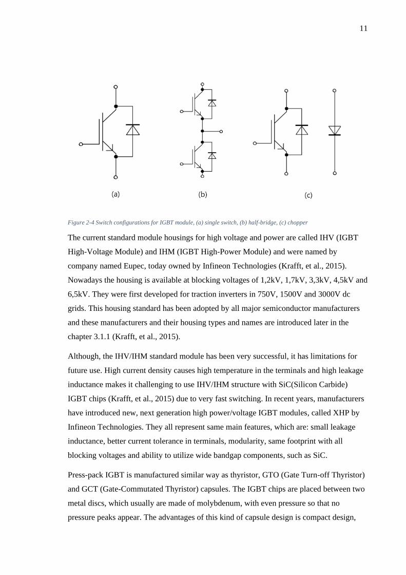
11
Figure 2-4 Switch configurations for IGBT module, (a) single switch, (b) half-bridge, (c) chopper
The current standard module housings for high voltage and power are called IHV (IGBT
High-Voltage Module) and IHM (IGBT High-Power Module) and were named by
company named Eupec, today owned by Infineon Technologies (Krafft, et al., 2015).
Nowadays the housing is available at blocking voltages of 1,2kV, 1,7kV, 3,3kV, 4,5kV and
6,5kV. They were first developed for traction inverters in 750V, 1500V and 3000V dc
grids. This housing standard has been adopted by all major semiconductor manufacturers
and these manufacturers and their housing types and names are introduced later in the
chapter 3.1.1 (Krafft, et al., 2015).
Although, the IHV/IHM standard module has been very successful, it has limitations for
future use. High current density causes high temperature in the terminals and high leakage
inductance makes it challenging to use IHV/IHM structure with SiC(Silicon Carbide)
IGBT chips (Krafft, et al., 2015) due to very fast switching. In recent years, manufacturers
have introduced new, next generation high power/voltage IGBT modules, called XHP by
Infineon Technologies. They all represent same main features, which are: small leakage
inductance, better current tolerance in terminals, modularity, same footprint with all
blocking voltages and ability to utilize wide bandgap components, such as SiC.
Press-pack IGBT is manufactured similar way as thyristor, GTO (Gate Turn-off Thyristor)
and GCT (Gate-Commutated Thyristor) capsules. The IGBT chips are placed between two
metal discs, which usually are made of molybdenum, with even pressure so that no
pressure peaks appear. The advantages of this kind of capsule design is compact design,

12
cooling on both surfaces and no wire bonds. On the other hand, there is no dielectric
insulation and when mounted, a defined uniaxial high pressure must be established and
maintained (Lutz, et al., 2018). Press-pack, IHV/IHM and XHP3 modules are shown in the
figure 2-5.
Figure 2-5 Module housings for IGBT, (a) Infineon Technologies IHV/IHM, (b) Infineon Technologies XHP3, (c) ABBs
Statpak (press-pack IGBT)
The packaging and switch configuration of the IGBT have major impact on the structure
and layout of the converter. The preferred housing and switch configuration are generally
determined by the system voltage and topology. More complex systems, as is the case in
multilevel MVD, have more semiconductor switches than 2-level converters, as can be
seen in the chapter 2.2. Each semiconductor switch requires a gate driver and therefore
adds costs and space requirements for the converter.

13
2.2 Converter
Converter is a device that transforms electrical power to different type of electrical power,
for example AC to DC, DC to DC, DC to AC or AC to AC. This thesis studies the high-
power converters for motor and generator drives. These types of converters are used in a
large field of applications, such as wind turbines, where generator feeds electrical power to
converter, which then transforms electricity eligible for the electrical grid. This chapter
will focus on the semiconductor devices of the converter since these contribute up to 40%
of the total material cost of an MVD (Sayago, et al., 2008 p. 3381).
Power converters can be either direct conversion, which are called AC-AC converters, or
indirect conversion, which have a dc-link. These indirect converters can be further divided
into a Current Source Inverters (CSI) or Voltage Source Inverters (VSI). VSI is by far the
most used converter type. In VSI the dc-link has direct voltage and in CSI, the dc-link has
direct current. The VSI uses relatively large capacitors as an energy storage, and CSI
relatively large inductor. (Pyrhönen, et al., 2016)
This chapter introduces most commonly used topologies in high power sector. To
understand basic power conversion, the 2-level VSI is studied first. The effect of levels is
then further explained through 3-level NPC and Cascaded H-Bridge (CHB) converter
topologies
2.2.1 2-level VSI
2-level VSI is an AC-DC-AC converter which contains rectifier (also called converter), dc-
link and inverter. The rectifier can be built with either passive diodes, or if bidirectional
power flow is needed, IGBTs. The diode rectifier is generally called DFE (Diode Front
End) and IGBT rectifier AFE (Active Front End), since it can be controlled. In 2-level VSI
with AFE, the grid converter and the motor inverter are identical, as we can see in the
figure 2-6.

14
Figure 2-6 Back-to-back 2-level VSI converter
The motor side inverter is connected to the + and - potentials of the DC bus, and these are
the two levels where the name comes from. The converter is modulated with PWM (Pulse
Width Modulation). Common PWM method is sine-triangle modulation, where triangular
carrier wave is compared with the reference sine waveform. Whenever the reference sine
wave is greater than the triangular wave, the referenced switch receives a pulse and starts
conducting. The triangle wave, the reference sine waves and resulting pulses can be seen in
the figure 2-7.
Figure 2-7 (a) Sine-triangle waveforms, (b) Phase U voltage (Pyrhönen, et al., 2016 p. 161)
To control the output voltage, amplitude modulation index is determined:
𝑚a =��ref
��tri
(2)

15
where ��ref is the peak reference voltage and ��tri the peak triangle voltage. Triangle voltage
peak is usually kept constant, so the control is done by varying the reference voltage (Wu,
et al., 2006 p. 97). For linear modulation, the ma needs to be ≤1. The peak output phase
voltage is then:
��ph =𝑈DC
2(3)
where UDC is the dc-link voltage. The line-to-line RMS voltage is calculated as:
Ud =√3
2√2𝑚aUDC ≈ 0.612𝑚aUDC (4)
When diode rectifier is used, the average value of the dc-link voltage is:
𝑈DC =1𝜋3
∫ √2
𝜋6
−𝜋6
𝑈LL cos𝜔𝑡 𝑑(𝜔𝑡) =3√2
𝜋𝑈o ≈ 1.35𝑈o (5)
Combining equations 4 and 5, the output voltage, when ma=1, is:
𝑈𝑑 ≈ 1.35 ∗ 0.612𝑈𝑜 = 0.83𝑈𝑜 (6)
As we can see, in linear modulation range the inverter does not produce as high output
voltage as the input voltage is. This means that if the converter is in 690V grid, the
maximum output voltage is approximately 573V (Pyrhönen, et al., 2016 p. 162). The
maximum output voltage can be increased by two methods, overmodulation and third-
harmonic reference injection.
As previously was stated, the linear modulation range is when ma≤1. Beyond this, starts the
overmodulation range and as modulation index is increased, the increase of line-to-line
voltage begins to decelerate, as can be seen in the figure 2-8.

16
Figure 2-8 Ratio of the output voltage fundamental to the DC-link voltage as a function of modulation index (Pyrhönen,
et al., 2016 p. 164)
Increasing the ma value to 2, the fundamental voltage can be increased to 0.744Udc, but
low-order harmonics are increased. If the ma is further increased to 3.24, the maximum
possible output voltage, 0.78UDC, is achieved which is 1.053 times the original input
voltage (Pyrhönen, et al., 2016 p. 163).
Output voltage can be also increased by extending the linear modulation range. This is
achieved with third-harmonic injection. A sine wave with frequency of three times the
reference frequency, is added to the sine-triangle comparison. This results in a flattened
peak in the modulated waves (dotted waves in the figure 2-9), and the fundamental waves
(coloured waves) can exceed the peak triangular wave (grey horizontal lines). The third
harmonic (black wave) does not increase harmonic distortion of line-to-line voltage since it
is common to all phases. With this method, the amplitude modulation index can be
increased by 15,5%, or in other words, to 1.155 without going to overmodulation. (Wu, et
al., 2006 pp. 99-100)

17
Figure 2-9 Sine-triangle modulation with third harmonic injection (Solbakken, 2017)
With the development of microprocessors, Space Vector PWM (SVPWM) has become one
of the most used modulation methods, especially in drives which require fast control. In
SVPWM, the desired voltage is produced by vectors. In three phase, two-level VSI
inverter, there are eight possible vectors, six active vectors and two zero vectors, each
active vector having magnitude of 2/3UDC. The vector space is divided into six sectors, as
seen in figure 2-10. It represents the three phases in 120° angle, with positive and negative
values.
Figure 2-10 Space vector modulation. (Pyrhönen, et al., 2016 p. 173)

18
Reference vector (uref in figure 2-10) rotates at same frequency as fundamental output
frequency. As the reference vector rotates from sector to sector, the different combinations
of switches are used to produce that reference vector. Vectors produced by switch
combinations are called stationary vectors, and three of stationary vectors are used to
correlate with reference vector. Dwell time is used for volt-second balancing, meaning that
the product of reference vector and sampling time is equal to the sum of voltage multiplied
by the time interval of stationary vectors:
{𝑢ref𝑇s = 𝑢1𝑇a + 𝑢2𝑇𝑏 + 𝑢0𝑇0
𝑇s = 𝑇a + 𝑇b + 𝑇c(7)
where voltages are as follows:
𝑢ref = 𝑢ref𝑒𝑗𝜃, 𝑢1 =
2
3𝑈DC, 𝑢2 =
2
3𝑈DC𝑒
𝑗𝜋3 , 𝑢0 = 0 (8)
Where ejθ is phase shift angle. Since the reference vector is produced with active vectors
with 2/3UDC voltage, the maximum uref voltage (circle in the figure 2-10) is:
𝑢ref,max =2
3𝑈DC ∗
√3
2=
𝑈DC
√3(9)
And the maximum output voltage is:
𝑈𝑜𝑢𝑡𝑝𝑢𝑡 = √3 ∗ (𝑢𝑟𝑒𝑓,𝑚𝑎𝑥
√2) = 0.707𝑈𝐷𝐶 (10)
When compared to the regular sine-triangle modulation, which had output voltage of
0.612UDC, a 15,5% increase is achieved, similar result as with the third harmonic injection
method.
2.2.2 3-level Neutral Point Clamped Inverter
In 2-level VSI inverter, one leg was composed of two switches which were attached to
positive and negative DC-buses. In 3-level Neutral Point Clamped (NPC) inverter, the
phase-leg has upper and lower branches with two switches similarly attached to positive
and negative DC-buses/terminals. The midpoints of these branches are connected with
diodes and form a neutral point. Now the inverter has positive, negative and neutral DC
terminals, in other words three voltage levels to which the output can be connected.

19
The NPC topology is somewhat similar to the 2-level VSI, as can be seen from the figure
2-11, but has double the switches and two additional power diodes per leg. The additional
level does however provide major benefits. Firstly, the output voltage waveform is much
more sinusoidal than in case of 2-level. Secondly, with the same voltage rated switches, the
NPC topology can produce higher output voltage than the 2-level, or the same output
voltage can be achieved with lower voltage rated devices.
In figure 2-11, the switching states of one leg of the NPC inverter is shown. The produced
voltages are +UDC/2, 0 and -UDC/2. The line-to-line voltage between legs can therefore
be +UDC, +UDC/2, 0, -UDC/2, -UDC, creating far more sinusoidal waveform than in 2-
level inverter. The switching frequency can also be reduced to produce same current THD
value as 2-level inverter, which would also reduce switching power losses. This might also
be necessary, because more switches mean more heat dissipation in the module. In
addition, the extra switches increase on state losses and require gate drivers, which raises
the auxiliary power consumption. (Semikron, 2015 pp. 2-3)
Figure 2-11 Topology of NPC leg with switching states and corresponding output voltages (Rodriguez, et al., 2009 p.
1789)
The control is also quite similar to the 2-level VSI, but slightly more complicated. This is
because the number of available switch combinations are increased to 27, which can
produce 18 different active and three zero vectors (Pyrhönen, et al., 2016 p. 171) . The

20
switch position combinations are presented in the table 2-1 and the resulting vectors in the
figure 2-12.
Table 2-1 Combinations of switch positions for 3L-NPC inverter
Combinations of switch positions
U + + + + + + + + + 0 0 0 0 0 0 0 0 0 - - - - - - - - -
V + + + 0 0 0 - - - + + + 0 0 0 - - - + + + 0 0 0 - - -
W + 0 - + 0 - + 0 - + 0 - + 0 - + 0 - + 0 - + 0 - + 0 -
Figure 2-12 Active vectors of 3-level NPC (Pyrhönen, et al., 2016 p. 172)
One disadvantage of the NPC topology is uneven heat dissipation between switches. The
current flow of the neutral point is naturally determined by the polarity since diodes are
used, and the blocking of the current flow from plus-terminal is done by turning the upper
switch (T1 in the figure 2-13) off. This means that the outer switches (T1 and T4 in figure
2-13) are switched off more often than inner switches (T2 and T3 in figure 2-13) and
therefore produce more switching losses. This leads to a reduction of maximum power
rating. To overcome this problem, actively controllable switches can be added to the
neutral point. This topology is called ANPC (Active Neutral Point Clamped).

21
Figure 2-13 Figure 2-13 Current paths during switching of one leg for one phase. Green represents the current flow
when the output phase voltage is 1 and blue when the output phase voltage is 0. (a) NPC topology, T1 handles the
current blocking (b) ANPC topology, T1 switches off, similarly to NPC (c) ANPC where T2 switches off and the neutral
current is forced to flow through lower neutral path
With ANPC topology, the distribution of power losses in semiconductor devices can be
adjusted and made better balanced and therefore, higher power rating can be achieved with
same rated devices. On the other hand, the higher number of switches increases the
semiconductor costs.
2.2.3 Cascaded H-Bridge Multilevel Inverter
Cascaded H-Bridge (CHB) Multilevel Inverter is an inherently modular topology, which
allows near sinusoidal output voltage. The H-bridge is a power conversion module, where
four switches are placed in a H-shape formation. Each H-Bridge need a Separate DC
Source (SDCS). These DC sources can be solar panels or fuel cells which makes it great
topology for renewable energy applications. The H-Bridge module can also include own
rectifying unit. In this kind of structure, a multi-phase input transformer is used to supply
each module.
Each H-bridge has two voltage source phase legs and single H-bridge can generate three
voltage levels. These H-bridges are then placed in series, in other words cascaded, and the
produced output voltage is the sum of each bridge voltage level. CHB has switch
combination redundancies that grows proportionally when the number of cells is increased.

22
The natural modular structure and redundancies enable fault-tolerant operation.
(Rodriguez, et al., 2009 pp. 1790-1791)
Figure 2-14 Nine-level CHB, a) topology structure, b) output voltage of each bridge and total output voltage. (Rodriguez,
et al., 2009 p. 1792)
2.2.4 5-level HNPC
5-level HNPC topology is a hybrid of NPC and CHB. The structure is similar to CHB, but
each cell has H-bridge with Neutral Point Clamped. The cell has therefore five voltage
levels: +UDC, +UDC/2, 0, -UDC/2, -UDC producing 9-level line-to-line voltage waveform,
eliminating the need for filtering. Similarly to CHB, each cell needs a separated DC
source, which is produced by multi-phase transformer and a rectifying unit. Each phase
(cell) has 12-pulse rectifier, resulting in 36-pulse rectification. This reduces the input
current THD by eliminating the low order harmonics, up to 25th. (Kouro, et al., 2010 p.
2556)

23
Figure 2-15 5-level HNPC converter with 36-pulse rectifier system and multi-phase transformer. The used semiconductor
switch is GCT thyristor. (Kouro, et al., 2010 p. 2556)
Though the 5-level HNPC converter has very low THD and filter less design, disadvantage
is the high number of components and the need for a special transformer. Compared to the
same level CHB, it has the same amount of components, plus 12 additional clamping
diodes and the need to control the neutral point of each cell (Kouro, et al., 2010 p. 2556).
While 5-level HNPC needs less components than NPC topology to produce same output
levels, it lacks the ability for 4-quadrant drive.

24
2.3 Reliability
Reliability is a major importance in high power applications. Even small interruptions in
critical applications can result in huge losses in profit. In offshore wind turbines, the access
to the turbine for maintenance is limited and can take even several days, meaning that
unexpected failure can lead to a huge amount of wasted energy production capacity.
In 2009, a survey was conducted by Yang et al. (2009) to study industries requirements
and expectations of reliability in power electronic converters. Questionnaire included five
topics:
- Responder categories and attitudes
- Reliability status and power device operating conditions
- Main stresses and deterioration indicators
- Load profiles, including load levels and duty times
- Failure counteractions and failure costs.
The study concluded that semiconductor devices were the most prone to fail component.
The system transients and overload conditions were considered to be the source of main
stresses and ambient temperature extremes, mechanical vibration and moisture the most
common environmental factors for failure. Interesting find was that applications with large
temperature swings, as is the case with wind turbine applications, the failure rates were
quite small, and where the temperature swings were small, the failure rates were relatively
high. The study considers that this is because extra demand on reliability gives opportunity
for better design tools and condition monitoring methods. (Yang, et al., 2009 p. 3156)
Failures can be divided into three categories: Early failures, random failures and end-of-
life failures. These failure categories are depicted in the figure 2-16 as function of
operation time and failure rate. Cause for early failures are usually from pre-damaging
during storage, transportation, assembly etc. End-of-life failures are inevitable and are
result of wearing from thermal-mechanical stress over time. Lastly, random failures are
failures that occur randomly over time. Reasons for random failures can be e.g. cosmic
rays, lightning or pollution. Since random failure rate is quite steady during whole device
lifetime, it can be expressed by FIT (Failures In Time), which represents the occurrence of
failures per every billion (109) hours. (Zhu, 2019 pp. 266-267)

25
Figure 2-16 The bathtub curve of failures (Zhu, 2019 p. 266)
In (Richardeau, et al., 2013), failure rate of a semiconductor device is calculated with the
following equation:
𝜆 = 𝜆0𝜋𝑡𝜋𝑠𝜋𝐸𝜋𝑞10−9/ℎ (11)
where λ0 is a failure rate reference at junction temperature of 100°C, πt is factor for
junction temperature different from 100°C and πs acceleration voltage breakdown for the
drain-source voltage by empirical relation. πE and πq are environmental and quality factors,
but these are not considered in this study since the environment is the same in all cases and
reliable quality factors could not be obtained. The equation for πt is:
𝜋t = 𝑒𝐾∗(
1𝑇𝑗1
−1
𝑇𝑗2)
(12)
Where K is the ratio of the energy activation and the Boltzmann constant. Junction
temperatures Tj1 and Tj2 are expressed with regard to absolute zero. The equation is then:
𝜋t = 𝑒4640∗(
1373
−1
𝑇𝑗+273)
(13)
and for πs
𝜋s = 0,22𝑒1,7(
𝑈ceoffstateUcerating
)
(14)
Where Uce_off_state is Udc and Uce_rating is the rated voltage of the device. If failure of one
device leads to a failure of whole system, the FIT rates of each device is added together to
produce a failure rate of the whole system. (Richardeau, et al., 2013 p. 4226)

26
The FIT rate can be derived to MTBF (Mean Time Between Failure), which translates to
the time, usually years, between failures in the system. The MTBF rate is calculated with
the following equation:
𝑀𝑇𝐵𝐹 =1
𝜆(15)
If the systems failure rate would be λ=0,00001 (failures per hour), the MTBF would
therefore be 100 000 hours or 11,4 years.

27
2.4 The economic effect of voltage
While this thesis focuses on the cost of semiconductors in MVD, it is only one factor when
selecting a VSD. Operator or customer needs to consider multiple other factors, such as
reliability and customer service. This chapter briefly introduces the Total Cost of
Ownership (TCO) and the factors that affect it but concentrates on the operating costs that
are impacted by the system voltage and moreover, how the MVD costs differ from LVD.
In a white paper, (Siemens, 2013), these TCO affecting components are listed as follows:
- Reliability
- Downtime
- Required maintenance
- Customer service and support
- Manufacturers reputation
- Spare parts acquisition and stocking
- Efficiency
- Price
The same paper shows results of a survey, where respondents ranked the importance of
factors. The results are shown below, and the percentage represents the number of
respondents who ranked each factor as critical of important:
1. Reliability, 97%
2. Customer service / support, 92%
3. Size of drive, 88%
4. Speed of delivery, 88%
5. Price, 86%
6. Ability to withstand harsh environments, 85%
7. Manufacturer’s reputation, 81%
8. Range of available options, 74%
This confirms that while price is important for customer, there are even more critical
factors that the supplier needs to meet.
Siemens (2018), compares the costs of LVD and MVD, in a medium voltage motor
application, meaning that when LVD is used, step-down and step-up transformers are

28
needed. The compared cost factors are cost of equipment, operation, installation and power
quality. The rest of this chapter analyses these factors briefly. Schneider Electric (2007)
also compares LVD and MVD in a medium voltage application.
Cost of equipment
According to the Siemens (2018), low voltage AC drive price can vary from 50% to 105%
compared to the MVD drive. Similar results are shown by Schneider Electric (2007),
where 300HP and 500 HP LVD is half of the MVD price, but in 800HP the prices are
almost equal. Additional step-up and step-down transformers increase the overall system
cost in LVD cases.
Cost of operation
Cost of operation is directly affected by the system efficiency. In LVD, the additional
transformers create power losses and reduces the overall efficiency. In (Siemens, 2018),
the compared MVD is a CHB topology that does not require additional filtering which
further increases the efficiency. This leads to operation costs that are half of the LVD
solution. If NPC topology would be used, filtering is required, and the difference would
not be so drastic. The system efficiency in 3-level NPC drive is nevertheless better than in
2-level VSI, as we can see later in the chapter 4.2.
Majority of the losses comes from drive and motor. Medium voltage motors are usually
slightly less efficient due the increased stator copper losses. According to Schneider
Electric (2007), the wiring losses are not more than four percent of the overall losses,
though the MVD has lower wiring losses. In the Schneider Electrics comparison, the LVD
has 20 to 25 percent greater losses which is largely result from the additional transformer.
Cost of installation
Since higher voltage reduces the operational current, smaller diameter cables can be used
in MVD and less copper is used, resulting in lower installation costs. The difference
between LVD and MVD installation cost increases disproportionately as the current
increases. In 250HP drive, the cost is 10 times higher in LVD and in 1000HP 24 times
according to Siemens (2018). However, Schneider Electric (2007) states that wiring costs
are relatively low portion of the overall project; in 800HP application the low voltage
wiring was approximately 15% and medium voltage wiring 7,5% of the total costs. Also,

29
the distance affects to the costs, since output filtering might be required in LVD because of
the less sinusoidal waveform than in multi-level converter.
Cost of power quality
Poor power quality can produce additional costs because of the repair or replacement of the
damaged equipment and lead to income losses due the downtime of production. Figure 2-
17 shows the frequency of power quality problems by industrial customers. Harmonics
were the second largest cause for power quality problems.
Figure 2-17 Frequency of power quality problems at customer sites (Siemens, 2018 p. 5)
Though harmonics rarely result into the process interruption, it has been studied to be
responsible for 5% of all power quality costs in the EU, meaning 8,4 billion USD, and 25%
of these costs were attributed to equipment damage or additional maintenance (Siemens,
2018 pp. 5-6). With multilevel converters, input harmonics can be reduced compared to
two-level design, thus resulting in better power quality and lower power quality costs.
Summary
It can be concluded, that the TCO is a complex figure that is influenced by multiple
factors. These factors can be equipment related, such as cost of equipment, or supplier
related, for example supplier reputation. The equipment related factors are also strongly

30
linked to the application in question and thus, no universal answer can be provided on
which system voltage is superior when TCO is considered.

31
3 Markets and the future trends
3.1 Market of semiconductors
Semiconductor industry has grown from 33 to 469 billion USD between 1987 and 2018
(Statista, 2019) and it is expected to grow to 543 billion USD in the year 2022 (Deloitte,
2019). Market share of power semiconductors was 37 billion USD in 2017 and is predicted
to increase to 52 billion USD by 2023, according to (Business Wire, 2018). Driving
technologies for the growth in power semiconductors are fifth-generation mobile
communication, renewable energy generation, electronic vehicles and consumer
electronics, but the growth is limited by lack of technological improvements in the power
semiconductors (Business Wire, 2018).
Though the power semiconductor market share is quite large, the IGBT modules are only
one tenth of it. The market share of IGBT modules varies between sources, but according
to Infineon’s quarterly update, the total market was 3,25 billion USD in 2018 (Infineon
Technologies, 2019 p. 36) and 3,93 billion USD in 2019 reported by MarketWatch (Market
Watch, 2019). The variance between sources can be a result of different definitions for
IGBT modules. Furthermore, only 11% of the IGBT market is high voltage IGBT’s (over
1700V) and is considered low volume. Medium volume applications use 1,2kV and 1,7kV
and are 53% of the IGBT market share. High volume applications, such as automotive
industry, use under 1,2kV IGBT and take 36% of the share (Hiller, 2017 p. 17).
The semiconductor market has been quite volatile in recent years. The industry suffered
shortages from commodity products, such as MOSFET’s between 2017 and 2018. This
was a result from overordering by end-customers which eventually proved to be
unnecessary. Industry overcame this shortage, since the demand for power semiconductors
decreased temporarily in 2019. Manufacturers also have difficulties in perceiving the
application sector’s needs. Orders for motor drives have been slowing down, but heavy-
duty industrial fans and blowers have been increased in demand. In renewable energy
sector, the wind energy market growth has started to stall but solar energy market is
growing. The US-China trade war has also distorted the market greatly. (IHS Markit, 2019)
The annual reports from Infineon and Fuji both state that the automotive industry is a big
factor in the semiconductor industry. Automotive semiconductors are already a 37,7 billion
USD industry and will grow rapidly in the near future, as can be seen from the table 3-1.

32
Table 3-1 Total number (millions) of electric vehicles and predictions for the next 10 years. Last row shows the todays
total cost of semiconductors per vehicle of each electric vehicle type. MHEV = Mild Hybrid Electric Vehicle, PHEV =
Plug-in Hybrid Vehicle, BEV = Battery Electric Vehicle. Source: (Infineon Technologies, 2019 p. 25)
MHEV [106] PHEV [106] BEV [106]
2018 0,3 2,9 1,7
2020 2,3 4,8 3,2
2025 20,6 10,5 10,2
2030 30,0 14,1 15,8
Total semiconductor cost
per vehicle 531$ 785$ 775$
Another large influencer in the market is the emerge of SiC (Silicon Carbide) components
to the market. According to (Grand View Research, 2019), the SiC power semiconductor
industry was worth 2,17 billion USD and is expected to grow annually 15,7% between
2018-2025, which can have a major impact on the market.
3.1.1 IGBT module manufacturers
This chapter focuses on the manufacturers that produce high voltage IGBT modules.
Infineon
Infineon is overwhelmingly the largest IGBT module manufacturer, having 34,5% of the
market share (Infineon Technologies, 2019 p. 36). Infineon provides the industry standard
IHV and IHM modules with 3,3kV, 4,5kV and 6,5kV blocking voltage. In 4,5kV, a single
module and a chopper module is available, single being 800A or 1200A and chopper
800A. The 800A single module is 140x130mm and 1200A and chopper are 140x190mm. It
uses IGBT3-L3, which is a Trench/Fieldstop IGBT. (Infineon Technologies, 2019a)
Infineon’s new generation high voltage IGBT module is called XHP3. It allows modular
design that enables scalability and has low stray inductance, which is important feature for
future SiC use. At the moment, only one XHP module is available in half-bridge
configuration, which is rated 3,3kV and 450A with dimensions of 140x100mm and
isolation voltage of 6kV or 10,2kV.
Mitsubishi
Mitsubishi is the second largest IGBT module supplier, according to the (Infineon
Technologies, 2019 p. 36), with market share of 10,4%. The industry standard 4,5kV IGBT
module is available at current ratings of 600-1500A. Versions are called H series, R series

33
and X series, X being the latest. Single module is available but no half-bridge or chopper
modules.
XHP equivalent is called LV100 and HV100 and difference between these two are the
isolation voltage, 6kV and 10,2kV respectively. LV100 will be available in 1,7kV and
3,3kV and HV100 is 3,3kV, 4,5kV and 6,5kV (Mitsubishi Electric Europe B.V., 2019).
Mitsubishi highlights easy paralleling, reduced temperature rise in terminals and low
internal inductance, similar to other manufacturers (Mitsubishi Electric, 2019).
ABB
ABB’s counterpart for IHV/IHM module is called HiPak, which is available in the
standard housing measures, 140x190mm, 140x130mm and 140x70mm. ABB IGBT
technology in HiPak modules is called SPT (Soft Punch Through), SPT+ and TSPT+.
Single switch IGBT modules range from 650A to 1200A and chopper module is available
in 800A. ABB also has a presspack module in 4,5kV, called StatPak, and current ranges
from 1300A to 3000A. XHP equivalent package is called LinPak, but it is only available in
1,7kV and 3,3kV. (ABB, 2018)
Hitachi
Hitachi has four different versions for 4,5kV modules, with current ratings ranging from
800A to 1500A. The difference between versions are in conduction losses, switching losses
and maximum allowed junction temperature. The E2 model represents low conduction
losses and E2-H low switching losses, both having maximum junction temperature of
125°C. The F and F-H are newer models that have maximum junction temperature of
150°C. The F version is featured to have similar attributes as E2 by representing low
conduction losses and F-H presented to have low switching losses, similar to E2-H. The
newest version is G/G2 and according to (Hitachi, 2018) is coming to mass production first
in 6,5kV and then 3,3kV. Schedule for 4,5kV version has not been published.
Next generation package, the XHP equivalent, is called nHPD2 (next High-Power Density
Dual), but its currently available only in 1,7kV and 3,3kV. It represents similar features as
other manufacturers of this type of packaging.

34
3.2 Assessment of the cost evolution of the HV-IGBT modules
Learning curve model is a method that is used to predict cost development of a product or
process. First empirical study of a learning curve was conducted by Theodore P. Wright in
1936, when he examined the manufacturing of airplanes. He observed that assembly costs
were reduced by a constant rate as the number of produced airplanes doubled (Anzanello,
et al., 2011). Later on, more industries have been studied and learning rates for different
products and processes have been obtained. With these rates, price reduction for certain
products can be predicted as the production is increased.
Learning curves can be calculated with one or multiple factors. These factors can be for
example learning by doing, learning by searching and learning by using. In the table 3-2,
the models, learning mechanisms and equations for these models are shown. One-factor
models usually result in higher learning rates than two-factor, but it is used in this study for
its simplicity and the limitations of available cost data.
Table 3-2 Classification of learning-curve models. CQ = reduced price , C1 = initial price , Q = cumulative production ,
KS = Knowledge stock, AS = Average scale, α,β,γ = learning-by-doing/-searching/-using elasticity (Zhou, et al., 2019 p.
3)
From the table, following one-factor equation is used:
𝐶𝑄 = 𝐶1𝑄−𝛼 (16)
where C1 is initial cost, Q cumulative production and α learning by doing elasticity. The
cumulative production of high voltage IGBT modules can be estimated from the rate of
estimated market growth of medium voltage converters. The market study (ARC Advisory
Group, 2018) estimates 18% growth in medium voltage converters between the years
2017-2022, which means 3,6% increase per year, resulting in the cumulative production of
6,52. This does not directly lead to a 18% growth in high voltage IGBT modules, since the
medium voltage converters can be built with lower voltage components, for example CHB,

35
but it is used in this calculation for demonstration. This assumption was made, since
reliable data on number of HV-IGBTs manufactured was not available.
The learning by doing elasticity, α, represents the learning rate. Learning rate (LR) is the
price reduction ratio of certain product when its production is doubled and is defined as
follows:
𝐿𝑅 = 1 − 2−𝛼 (17)
In (Auerswald, et al., 1998 p. 43), 20% learning rate for semiconductors was proposed,
which translates to a learning by doing elasticity of 0,3219. Now the reduced price can be
calculated using equation (15). This results in approximately 45% reduction on price by
2022. With learning rate of 30%, which has been achieved in solar and wind industries
(Elshurafa, et al., 2018 p. 3), the price reduction by 2022 would be approximately 62%. On
the other hand, if the learning by doing would be relatively slow in the following years, for
example 5% which is quite typical for mature technologies such as nuclear and coal
industries, the price would reduce only 13%.

36
3.3 Market of the MVD
Since the emphasis of this study is on medium voltage drives, this chapter will focus on
this market. However, for comparison the overall drives market is estimated to be
approximately 9 (Mordor Intelligence), 17 (Global Market Insights) or 20 (Markets and
Markets) (Research Nester) billion USD. The large difference in estimations probably
come from the differences in the definition of variable speed drive. The majority of the
revenue comes from low voltage drives, since the medium voltage drives market is
estimated to be approximately 2 billion USD (ARC Advisory Group, 2018).
The largest industries of medium voltage drives are metal, marine, oil and gas, electric
power generation and mining industry, comprising almost 70% of the medium voltage
drive market share. Of these industries, oil and gas and mining are expected to grow with
annual rate of over 3,3% between 2017-2022. Other top industries are estimated to grow
also but with lower rate. One of the contributors for growth is the need for more
environmentally friendly production and therefore improved energy efficiency. Other
factors are urbanization, new middle class, infrastructure investments and global need for
clean water. There are, however, some uncertainties in the market, for example ongoing
trade war between USA and China, Brexit etc. that can affect on the development of the
market. (ARC Advisory Group, 2018)
Medium voltage drives have a market share of 20% in the marine industry, rest being low
voltage drives. The marine industry was valued at 772 million USD in 2019. The segment
proportion is expected to remain the same in the year 2024 but is predicted to grow from
151 million USD to 209 million USD. The reduction of the cost of operation with medium
voltage VSD is forecasted to drive the growth of the market. Marine applications that use
medium voltage drives are propulsion systems, thrusters, auxiliary system, winches, etc.
(Markets and Markets, 2019b)
The biggest manufacturers of medium voltage converters are ABB, Siemens, General
Electric, Toshiba Mitsubishi-Electric Industrial Systems Corporation (TMEIC) and
Rockwell, possessing over 65% of the market share. The medium voltage converter
portfolios of selected manufacturers are described in more detail below, emphasising the
VSI products. Technical parameters introduced for the converters are topology,
semiconductor type and blocking voltage and coolant type (air/water).

37
ABB
ABB is the biggest provider of medium voltage drives in the market. It has wide portfolio
of medium voltage drives, ranging from 200kW to 36MW in VSI drives and up to 150MW
in CSI drive. Used topologies are 3-level NPC, 5-level ANPC and CHB, and preferred
semiconductor type is IGCT but HV-IGBT is used in ACS2000 and LV-IGBT in
ACS580MV. All relevant output voltages are available, ranging from 2,3kV up to 13,8kV.
The model names for VSI converters are ACS1000, ACS2000, ACS5000, ACS580MV,
ACS6000 and ACS6080.
Siemens
Siemens is a close second in the medium voltage drive market. It provides all relevant
topologies of medium voltage sector: CHB, M2C (Modular Multilevel Converter), NPC,
CC (Cycloconverter) and LCI (Load Commutated Inverter). All relevant output voltages
are also available and the power of VSI converters range from 1MW to 46,7MW.
The model names for VSI converters are Sinamics Perfect Harmony GH150 (M2C) and
GH180 (CHB), Sinamics GM150 and Sinamics SM150. Sinamics, GM150 and SM150,
are both 3-level, but GM150 uses DFE and SM150 has AFE. Both are available with HV-
IGBT or IGCT. GM150 is available with output voltage of 2,3kV, 3,3kV and 4,16kV with
HV-IGBT and 3,3kV with IGCT. SM150 has 3,3kV with both semiconductor types, but
4,16kV is available only with IGBT. (Holopainen, 2019 pp. 26-27)
General Electric
General Electric has third largest market share in the medium voltage drives. It provides
only two VSI converter models: MV6 and MV7000. The MV6 model has a nested neutral
point piloted (NPP) topology, which is only used by the GE from the top five
manufacturers. NPP is a hybrid drive that combines the NPC and FC (Flying Capacitor)
topologies (Holopainen, 2019 p. 29). It is available in output voltages from 2,3kV to 6,9kV
and output power range from 160kW to 3,15MW. Possible output voltage levels are 3-
level, 5-level and 9-level and used semiconductor is IGBT. Both, DFE and AFE are
available.
MV7000 has two different versions, flat pack and press pack. The latter, as the name
suggests, uses press pack IGBTs. For the flat pack version, there is no clear information of
what IGBT type it uses. Flat pack version ranges from 3,3kV to 6,6kV and 0,7MW to

38
10MW and is air- or water-cooled. Press pack model is available from 3,3kV to 13,8kV
and 3MW to 81MW with water-cooling only. Both, DFE and AFE are available.
Toshiba Mitsubishi-Electric Industrial Systems Corporation
Toshiba Mitsubishi-Electric Industrial Systems Corporation (TMEIC) has 10 different
models which cover output voltages from 1,25kV to 11kV and power outputs of 100kW to
100MW. Available topologies are CHB, 3-level NPC and 5-level HNPC. MVe2 and
MVG2 are CHB converters that uses 3-level power cells. The major difference between
these two is that MVe2 has AFE in the power cell, allowing bidirectional power flow,
while MVG2 uses diode rectifiers. The NPC converters are listed in the table 3-3.
The power semiconductors that TMEIC uses are IGBT, HV-IGBT, IEGT (Injection
Enhanced Gate Transistor) and GCT. It can be noted that TMEIC offers wide range of
products for wide range of applications, similar to ABB and Siemens.
Rockwell Automation
Rockwell Automation has quite limited offering, though it is the fifth largest medium
voltage drive supplier. It has only two converters, PowerFlex 6000 and PowerFlex 7000.
PowerFlex 6000 is standard CHB topology with 2-level power cells. PowerFlex 7000 is a
CSI converter that utilizes SGCT’s (Symmetrical Gate Commutated Thyristors), it is
available for 2,4kV, 3,3kV, 4,16kV and 6,6kV voltage levels, power ranging from 150kW
to 6MW. Rockwell Automation differs from other top manufacturers in that it does not
have a product that utilizes NPC type topology.
Yaskawa
Yaskawa offers one MVD named MV1000. Used topology is 3-level CHB with two power
cells in one phase in series, producing 17-level output voltage. MV1000 is available with
five voltage ratings, 2,3kV, 3,3kV, 4,16kV, 6,6kV and 11kV and power ranges from
200HP to 16000HP. (Yaskawa America Inc., 2018)
Manufacturer summary
Most common topologies in MVD seems to be CHB, 3L-NPC and 5L-ANPC. Naturally
the most common semiconductor in CHB is IGBT and in NPC topologies, HV-IGBT and

39
IGCT/GCT. Insulated HV-IGBT is mostly used under 15MW range and above that, press
pack IGBT or IGCT are used. Output power is not bound to certain topologies, but under
5MW the preferred topology tends to be CHB or 3L-NPC with insulated HV-IGBT.
Since the spectrum of used topologies, semiconductors, output voltages and output powers
is so wide, no straightforward answer on the preferred type can be found to any power or
voltage level. This can be consequence of that the MVD industry is still uncertain about the
optimal converter type or that the medium voltage applications vary so much, that the
product portfolio needs to be versatile.
Converter manufacturers using NPC topology are shown below. Note that majority of the
listed converters had possibility of a higher output frequency on request. More extensive
table including CHB topologies can be found in the appendix I.

40
Table 3-3 NPC converters from top 5 manufacturers
Manufacturer Model Topology Voltage (kV) Power (MVA) Semiconductor
Grid
interconnection
Output
frequency
(Hz)
ABB
ACS1000 3L-NPC 2,3 - 4,16 0,315-5 IGCT DFE 0 – 82,5
ACS2000 5L-ANPC 4,16 - 6,9 0,25-3,68 HV-IGBT DFE/AFE 0 - 75
ACS5000 5L-ANPC 6,0 - 13,8 2,0 - 36,0 IGCT DFE 0 - 250
ACS6000 3L-NPC 2,3 - 3,3 5,0 - 36,0 IGCT DFE/AFE 0 - 75
ACS6080 3L-NPC 2,3 - 3,3 5,0 - 36,0 IGCT DFE/AFE 0 - 100
Siemens
GM150 3L-NPC 2,3/3,3/4,16 1,0 - 13,0 HV-IGBT DFE max 250
3,3 10,0 - 21,0 IGCT DFE max 250
SM150 3L-NPC 3,3/4,16 3,4 - 7,2 HV-IGBT AFE max 250
3,3 10,0 - 30,0 IGCT AFE max 250
GE
MV6 NPP 2,3 - 6,9 0,16 - 3,15 IGBT DFE/AFE 0 - 75
MV7000 flat
pack 3L/5L-ANPC 3,3 - 6,6 0,7 - 10,0 HV-IGBT DFE/AFE 15 – 90
MV7000 press pack 3L/5L-ANPC 3,3 - 13,8 3,0 - 81,0 HV-IGBT DFE/AFE
15 – 90
TMEIC
Tmdrive-30 3L-NPC 1,25 1,7 - 4,0 IGBT DFE/AFE 0 - 120
Tmdrive-50 3L-NPC 3,3 1,5 - 6,0 HV-IGBT AFE 0 - 60
Tmdrive-70e2 3L-NPC 3,3 4,0 - 36,0 IEGT AFE 0 - 75
Dura-Bilt5i 3L-NPC 2,4/4,2 0,15 - 7,5 HV-IGBT DFE 0 - 120
Tmdrive-XL55 5L-HNPC 6,6 4,0 - 16,0 HV-IGBT DFE max 250
Tmdrive-XL75 5L-HNPC 6 10,0 -92,0 IEGT DFE 50 - 200
Tmdrive-XL80 3L-NPC 3,8 10,0 - 30,0 GCT DFE 50 - 200
Tmdrive-XL85 5L-HNPC 7,2 15,0 - 120,0 GCT DFE 50 - 200

41
4 Topology comparison
This thesis compares different power modules where the ratio of cost and power is
considered. Five different cases were chosen for the comparison, where the main variables
are output voltage, topology and used IGBT module. The effect of gate drivers to the cost
and structure are not considered in this study. The load type is selected to be maximum
continuous load. The performance of the cases are simulated with the semiconductor
suppliers own simulation tools. Additionally, the reliability of each case is calculated with
the equations introduced in the chapter 2.3, using the results from the simulations.
A similar study, (Sayago, et al., 2008) was conducted in 2008, where costs of power
modules were compared. The difference to this study is that it only compared different
voltage levels of the NPC structure (2,3kV, 3,3kV and 4,16kV) and the costs of gate
drivers and heat sinks were included to the costs of power module. It also compared the
effect of switching frequency and modulation method. The load cycle is likewise different
since the old study uses rolling mill as a reference application, whereas this study simulates
the maximum continuous load. Nevertheless, (Sayago, et al., 2008) shows that the research
method of this study is appropriate and relevant. It can also be used as a reference study to
see, how the medium voltage converters have evolved in ten years of time in costs and
power.
4.1 Research method
The five different converter cases are shown in the table 4-1.
Table 4-1 Simulation cases for cost comparison
Output voltage Topology IGBT module
Case 1 690V 2-L VSI Half-bridge, 1700V
Case 2 1000V 3L-NPC Half-bridge with integrated NPC diode 1200V
Case 3 3300V 3L-NPC Single, 4500V
Case 4 3300V 3L-NPC Chopper, 4500V
Case 5 3300V 3L-CHB Half-bridge with integrated NPC diode, 1200V
Case 1 represents the most commonly used converter type, two-level VSI, with 1700V
IGBT modules. Case 2 is a low voltage, three-level NPC converter which uses recently
launched 1200V half bridge IGBT module with integrated NPC diode. This allows a

42
compact design and reduced costs compared to medium voltage, since low voltage
components are far more inexpensive.
Cases 3 and 4 are otherwise similar to each other, but different IGBT modules are used. In
case 3, single switch modules are used with separate clamping diodes. In case 4, a
combination of chopper and single switch modules are used. The use of chopper module
eliminates the need for separate clamping diodes, since the modules have additional diode,
as can be seen in the figure 4-1.
Lastly, case 5 is a CHB converter which uses two three-level cells per phase, producing
3,3kV output voltage and nine-levels per phase. 1200V half-bridge IGBT modules are
used, same as in case 2.
Figure 4-18 One leg of each case. Component type is marked with coloured square. (a) 690V 2L-VSI, (b) 1000V 3L-NPC,
(c) 3,3kV 3L-NPC with single switches, (d) 3,3kV 3L-NPC with chopper + single switches (e) 3,3kV 3L-CHB, one cell.
Colours: Grey = Half-bridge, black = half-bridge with integrated NPC diode, blue = single switch, red = NPC diode,
green = chopper
As can be seen from the figure 4-1, multilevel structure adds complexity and increase the
number of components. As was mentioned in the chapter 2.1, each semiconductor switch

43
requires a gate driver which adds more costs and increase space requirements of the
converter. The gate driver costs are however not included in this cost comparison.
To each case, a unit cost is calculated, which can be used to analyse and compare the costs
of each case. The phase power is calculated using semiconductor manufacturers simulation
tools, IPOSIM (Infineon Techologies, 2020) and Semisel (Semikron, 2020). Price data for
semiconductors in case 3 and 4 were provided for Yaskawa by suppliers. For case 3, price
information from four suppliers were obtained. In case 4, two prices were obtained, since
only two suppliers were providing chopper modules. Price for low voltage IGBT module
was available internally. In cases 2 and 5, where one specific module was used, the actual
price was not available, and an estimate has been done by analysing price data of similar
components. Costs of semiconductors per delivered maximum output power per phase,
marked with symbol X, is calculated as
𝑋 =𝑛𝐶
𝑆ph, (18)
where n is number of components, C the price of the module and Sph the phase power.
Another comparison figure is the maximum output power per component base plate area to
illustrate the power density Y. Since the dimensions of each component is known, the
power density is:
𝑌 =𝑆ph
𝑊 ∗ 𝐿 ∗ 𝑛, (19)
where W and L are the width and length of the component in question.
Finally, reliability is considered. Reliability is calculated with equations from the chapter
2.3. As was previously stated, only πt and πs are considered, since environmental factor πE
is same in all cases and appropriate quality factors πq for different components are not
available.
44
4.2 Simulation tools
Infineon’s simulation tool, IPOSIM, is used in three of the cases (1, 3 and 4). The
simulation process is divided into five sectors. First, the desired topology is selected. There
are multiple options from different applications, but only two are used in this study, three-
phase two-level and three-phase three-level NPC1.
When topology is selected, circuit and control parameters are specified. Available control
algorithms are sine-triangle and space vector modulation, latter being used in these
simulations. In three-level topologies, a circuit configuration is also determined. Circuit
configuration determines, which type of components are used to achieve the three-level
structure. For example, in case 3, single switch with extra diodes are chosen and in case 4,
FD/DF combination is selected. Next, a DC link voltage is determined. DC link voltage is
simply the peak value of the output voltage:
𝑈𝐷𝐶 = √2 ∗ 𝑈𝑜𝑢𝑡𝑝𝑢𝑡 ∗ 1.13, (20)
where the coefficient 1.13 is used to take account the imperfections of real system, control
reserve, voltage drops etc. In three-level applications, this is further divided by 2. IPOSIM
then automatically applies the required blocking voltage according to the DC link voltage.
After this, the rms value of the output current is adjusted. The goal is to find the highest
possible output current, in other words output power, with maximum junction temperature
being 125°C. Output frequency is 50Hz in every case and modulation index and power
factor is kept at 1. The switching frequency varies depending on the case. In medium
voltage cases, the switching frequency was chosen to be 1050Hz similar to (Sayago, et al.,
2008) and VACON® 3000, which is a MVD with NPC topology manufactured by Danfoss
(Danfoss Drives, 2019). In low voltage, 3000Hz switching frequency is used, which is
typical value for ABBs ACS880 low voltage drive module (ABB, 2020 s. 193). The
selected input parameters for cases 1, 3 and 4 are listed in the table 4-2.
Once the circuit and control parameters are determined, the used device is selected.
IPOSIM shows the applicable devices for the selected topology and parameters. When the
desired module is chosen, the cooling conditions are specified. In this study, fixed heatsink
temperature of 70°C is used. In advanced parameters, the gate resistors can be individually
determined. The default values for the selected devices are used in this simulation. If the
above parameters are selected accordingly, the simulation can be run. The result page

45
shows the maximum junction temperature, switching losses, conduction losses and total
losses for each switch and diode in the circuit.
Semikron’s Semisel follows a similar pattern. Semisel is used in cases 2 (and 5), because
Semikron offers a specific module for this kind of application. First, three-level inverter is
selected from the DC/AC dropdown menu. Next, circuit parameters are determined, much
like in IPOSIM, with the addition of overload parameters. Overload is not taken into
consideration in this simulation, so factor is chosen 1 and min. output frequency 50Hz.
Parameters are listed in the table 4-2. Note that in Semisel, the DC Link Voltage is the
voltage between + and – terminals, which translates to 1500V in case 2, but is listed as
750V in the table similar to IPOSIM.
Table 4-2 Input parameters. (SVM=Space Vector Modulation)
Case 1 Case 2 / Case 5 Case 3 / Case 4
Control Algorithm SVM SVM SVM
Circuit Configuration - - Single Switch With Extra Diode / FD/DF Combination
DC Link Voltage 1050V 750V 2650V
Blocking voltage 1700V 1200V 4500V
Output Current (rms) 880A 800A 375A
Output Frequency 50Hz 50Hz 50Hz
Switching Frequency 3000Hz 3000Hz 1050Hz
Modulation Index 1 1 1
Power Factor cos(ϕ) 1 1 1
As in IPOSIM, the desired device is selected next. From calculation method, “use
maximum values” is chosen and other options are kept as default. Finally, the heat sink
parameters are set. As was in IPOSIM, the heat sink can be specifically determined, but in
this study, the fixed heat sink temperature of 70°C is used. Now the simulation can be run,
and the tool returns same results as in IPOSIM. Although the maximum junction
temperature was only 104°C with these parameters, the output current was set to 800A to
leave a buffer since the rated current of the used module was 1200A.

46
4.3 Results
Table 4-3 shows the simulation results of each case. Junction temperature of 125°C was
achieved with cases 1, 3 and 4. In cases 2 and 5, the maximum junction temperature was
only 102°C, but the current was not raised further, since a buffer is needed between
operating current and rated current for reliability reasons. The switching frequency could
be increased quite significantly, but this would raise switching losses and reduce overall
efficiency.
Table 4-3 Simulation results
Case 1 Case 2 Case 3 Case 4 Case 5
Max junction temperature
Switch (outer) 124,9°C 102°C 124,8°C 124,8°C 102°C
Switch (inner) - 96°C 80,7°C 80,7°C 96°C
Diode 93,5°C 79°C 70,3°C 70,3°C 79°C
FWD - 90°C 114,7°C 114,7°C 90°C
Total losses 2238W 1779W 3346W 3346W 7116W
Phase powers, cost ratios, power densities and efficiencies are listed below in table 4-4. In
case 2, the power is increased by 31,6% with higher efficiency when compared to common
2-level design. This comes with a two to three times higher cost and power density is
reduced by almost 40%.
In medium voltage cases 3 and 4, the power is doubled, but power density is only half of
the case 1. Semiconductor costs range from 3 to 7 times the common design, depending on
the module type and the supplier. Efficiency is slightly higher.
Table 4-4 Results. The semiconductor cost per kVA ratio is the cost compared to the case 1
Case 1 Case 2 Case 3 Case 4 Case 5
Output voltage (V) 690 1000 3300 3300 2000
Output current (A) 880 800 375 375 800
Phase power (kW) 351 462 714 714 924
Cost per kVA ratio 1 2,0 - 2,8 4,2 - 6,9 3,1 - 6,0 4,3 - 6,1
kVA per square cm 1,6 1,0 0,7 0,8 0,51
Efficiency (%) 99,36 99,61 99,53 99,53 99,23
For cases 3 & 4, power and current were kept constant so only variable was the price of the
modules. Different modules from different suppliers, however, produce different powers.
To better compare the performance, comparison between 1200A rated single modules was

47
conducted, since the price of these modules were available and each of these three
suppliers had their own simulation tool. The output power was significantly higher, but the
cost per kVA was similar to 800A devices.
Table 4-5 Results of the 1200A rated devices. The semiconductor cost per kVA ratio is the cost compared to the case 1
Supplier 1 Supplier 2 Supplier 3
Phase power (kW) 1048 838 1124
Cost per kVA ratio 6,1 4,6 4,7
Since the simulation gives results for maximum junction temperature of each switch and
diode, the failure rate can be calculated. This is not an accurate calculation of the system
reliability, but an example to study differences of reliability between different topologies.
For the calculations, base value λ0=5000 (Richardeau, et al., 2013 p. 4226) for IGBT
module (including diode) is used and λ0=3000 (Department of Defense, 1991 p. 55) for
clamping diode. The value of πs is same to each component in the same voltage class, but
the πt varies between inner and outer switches and clamping diodes, so the FIT rates for
these are calculated independently. Using equations (11), (13) and (14), the following
failure rates are obtained:
Table 4-6 Component failures per phase in hour rate
Switch (outer) Switch (inner) FWD
Switch
(outer)
Switch
(inner) FWD
λ1 (10-6) λ2 (10-6) λ3 (10-6) n1 n2 n3
Case 1 3,9 - - 2 - -
Case 2 1,9 1,6 7,7 2 2 2
Case 3 & 4 3,7 8,6 1,6 2 2 2
Case 5 1,9 1,6 7,7 4 4 4
Multiplying the device failure rates with the number of each component (n1, n2 and n3) and
adding all failure rates of each case together, system failure rates per phase is obtained.
Multiplying this by three, the resulting system failure rates for the three-phase system are:
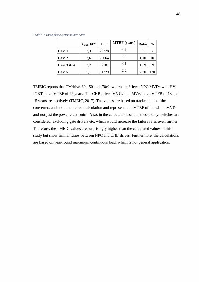
48
Table 4-7 Three-phase system failure rates
λtotal (10-6) FIT MTBF (years) Ratio %
Case 1 2,3 23378 4,9 1 -
Case 2 2,6 25664 4,4 1,10 10
Case 3 & 4 3,7 37101 3,1 1,59 59
Case 5 5,1 51329 2,2 2,20 120
TMEIC reports that TMdrive-30, -50 and -70e2, which are 3-level NPC MVDs with HV-
IGBT, have MTBF of 22 years. The CHB drives MVG2 and MVe2 have MTFB of 13 and
15 years, respectively (TMEIC, 2017). The values are based on tracked data of the
converters and not a theoretical calculation and represents the MTBF of the whole MVD
and not just the power electronics. Also, in the calculations of this thesis, only switches are
considered, excluding gate drivers etc. which would increase the failure rates even further.
Therefore, the TMEIC values are surprisingly higher than the calculated values in this
study but show similar ratios between NPC and CHB drives. Furthermore, the calculations
are based on year-round maximum continuous load, which is not general application.

49
5 Analysis of the results
The results show that increased voltage and extra level increase power quite significantly,
especially in medium voltage cases 3 and 4, where the power was doubled. The NPC
structure however increase the number of components and leads to a lower power density.
More complex system also increases the number of gate drivers, which further increase the
costs and space requirements. On the other hand, the output is more sinusoidal, which
reduces the size of filters, and the overall space requirement may not be that different.
Efficiency is also enhanced, which is a major benefit for example in energy production
applications. Power losses in medium voltage cases are still far larger, because of the
increased power, which means that bigger cooling equipment is required. In case 2, the
power is increased, but also the efficiency, because of the slightly lower power losses than
in case 1.
The increased number of components in NPC structure increase the failure rates of the
system. In cases 3 and 4, the increase is considerable, which is great concern in critical
processes. However, the reliability can be increased substantially with appropriate design,
as was stated in the chapter 2.3. With this type of calculation, the failure rates of CHB are
overwhelmingly the largest, but the redundancies enable fault-tolerant operation and
modular construction makes the replacement of the module easy, which increases the
availability. The case 2 has surprisingly low increase in failure rate, even though it has
twice the modules and more components in those modules than case 1. Reason for this is
the lower junction temperatures in the switches.
Though the power is increased greatly compared to case 1, the costs are also expanded.
Naturally the number of components increase the costs, but also the high voltage IGBT
modules are far more expensive than low voltage ones, since the market of the medium and
high voltage IGBT modules is quite marginal compared to low voltage. This leads to 3-7
times higher semiconductor costs in cases 3 and 4, compared to case 1. The difference in
costs in case 2 is not that significant, since the 1200V IGBT modules have even bigger
market share than 1700V IGBT modules (Hiller, 2017 p. 17).
As was reviewed in chapter 3.3, there is no sight of major growth in MVD market, which
directly would influence the price development of the high voltage IGBT modules. In
chapter 3.2, the cost development analysis showed that considerable price reduction is

50
possible but resulting cost is still considerably greater than low voltage module costs. Also,
there is module competition within the MVD market since it is divided with topologies that
use LV-IGBT and HV-IGBT. This causes uncertainty about the future of the HV-IGBT.

51
6 Conclusions
In this thesis, a cost and reliability comparison between five selected power converter
topologies was conducted. The cases were industry standard 2-level VSI, 3-level 1000V
NPC, 3-level 3300V NPC, with single or chopper modules, and 3300V CHB. First, used
IGBT modules and topologies in MVD market were introduced. The market situation was
further studied and price development of the HV-IGBT modules was estimated. Also,
reliability calculations for power modules were demonstrated.
The cost comparison was generated by simulating the performance of each case. The
results show that while medium voltage NPC structure provides major increase in power
output, the semiconductor cost is multiple times larger than the standard 2-level LVD. The
reliability is also reduced, which further increases the operational costs, though reliability
can be greatly affected by proper design. Cost development estimations showed, that the
price reduction in the near future would not be enough to approach the costs of LVD.
The 3-level 1000V NPC structure proved to be a cost-effective solution. The power was
increased greatly, and the costs were significantly lower than with medium voltage. This
was achieved with marginal decrease in reliability. Also, increase of power density and
price reduction of 1200V modules could be far greater and faster than of HV-IGBT, since
the 1200V modules are mass produced.
The study succeeded in its main goal to provide cost comparison for the chosen topologies.
With the developed method, other topologies and modules can be compared in the future if
price data for those modules are available. The market study section of the thesis could not
provide conclusive answers to where the markets are developing, though this could mean
that there is a lot of uncertainty in the market and the development should be observed
constantly.
Further investigation should be made about how much different topologies affect on prices
of other equipment of the converter, for example filters, circuit breakers, busbars, cablings
and to maintenance costs. Impact of different converter topologies to electrical machine
structure and cost could also be investigated in further studies.

52
REFERENCES ABB. 2020. ABB industrial drives. ABB homepage. [Online] 2020. [Cited: 24 March
2020.] https://search-
ext.abb.com/library/Download.aspx?DocumentID=3AUA0000128301&LanguageCode=en
&DocumentPartId=1&Action=Launch.
—. 2018. Library. ABB homepage. [Online] 2018. [Cited: 12 December 2019.]
http://search.abb.com/library/Download.aspx?DocumentID=5SYA2109&LanguageCode=
en&DocumentPartId=&Action=Launch.
Anzanello, Michel Jose and Fogliatto, Flavio Sanson. 2011. Learning curve models and
applications: Literature review and research directions. s.l. : Elsevier, 2011.
ARC Advisory Group. 2018. Medium voltage AC drives global market 2017-2022. s.l. :
ARC Advisory Group, 2018.
Auerswald, Philip, et al. 1998. The Production Recipes Approach to Modeling
Technological Innovation: An Application to Learning by Doing. s.l. : SANTA FE
INSTITUTE, 1998.
Baliga, Jayant B. 2018. Fundamentals of Power Semiconductor Devices. s.l. : Springer
International Publishing 2019, 2018.
Business Wire. 2018. News. Business Wire homepage. [Online] 2 October 2018.
https://www.businesswire.com/news/home/20181002005795/en/Global-Power-
Semiconductor-Market-2017-2018-2023-Analysis.
Danfoss Drives. 2019. A modular and configurable cabinet-built drive delivering superior
performance . s.l. : Danfoss Drives, 2019.
Deloitte. 2019. Semiconductors – the Next Wave. s.l. : Deloitte, April 2019.
Department of Defense, Washington DC. 1991. MIL-HDBK-217 (Military Handbook for
Reliability Prediction of Electronic Equipment). s.l. : Department of Defense, Washington
DC, 1991.
Elshurafa, Amro M., et al. 2018. Estimating the learning curve of solar PV balance–of–
system for over 20 countries: Implications and policy recommendations. s.l. : Elsevier,
2018.
Finnish Ministry of the Environment. 2019. IPCC: Ilmasto lämpenee hälyttävällä
vauhdilla. Homepage of Ministry of the Environment. [Online] 15 10 2019.
https://www.ym.fi/fi-
FI/Ajankohtaista/IPCC_Ilmasto_lampenee_halyttavalla_vauhd(48136).
Global Market Insights. Industry analysis. Global Market Insights homepage. [Online]
[Cited: 12 December 2019.] https://www.gminsights.com/industry-analysis/variable-
frequency-drive-vfd-
market?utm_source=prnewswire.com&utm_medium=referral&utm_campaign=Paid_prne
wswire.

53
Grand View Research. 2019. Industry analysis. Grand View Research homepage.
[Online] July 2019. [Cited: 12 December 2019.]
https://www.grandviewresearch.com/industry-analysis/silicon-carbide-market.
Hermwille, Markus. 2007. Application Note AN-7003. Gate Resistor – Principles and
Applications. s.l. : SEMIKRON INTERNATIONAL GmbH, 12 November 2007.
Hiller, Marc. 2017. Power Electronics for Medium Voltage Grid - Topologies and
Semiconductors. s.l. : Electrotechnical Institute (ETI), 2 February 2017.
Hitachi. 2018. Overview of Hitachi IGBT. s.l. : Hitachi, 2018.
Holopainen, Antti. 2019. Multilevel voltage source inverters in medium voltage drives.
s.l. : LUTPub, 26 February 2019.
IHS Markit. 2019. Market Insight. IHS Markit homepage. [Online] 18 June 2019.
https://technology.ihs.com/615088/highlights-from-pcim-europe-2019-the-power-
semiconductor-market-is-slowing.
Infineon Technologies. 2019. Fourth Quarter FY 2019 Quarterly Update. Quarterly
Financial Results. 12 November 2019.
—. 2019a. Products. Infineon Technologies homepage. [Online] 2019a. [Cited: 12
December 2019.] https://www.infineon.com/cms/en/product/power/igbt/igbt-
modules/ihv_4500v/.
Infineon Techologies. 2020. IPOSIM simulation tool. Infineon Techologies homepage.
[Online] 2020. [Cited: 5 January 2020.]
https://www.infineon.com/cms/en/tools/landing/iposim.html.
Iwamuro, Noriyuki and Laska, Thomas. 2017. IGBT History, State-of-the-Art, and
Future Prospects. IEEE Transactions on Electron Devices. s.l. : IEEE, 13 February 2017.
Kouro, Samir, et al. 2010. Recent Advances and Industrial Applications of Multilevel
Converters. IEEE Transactions on Industrial Electronics ( Volume: 57 , Issue: 8 , Aug.
2010 ). s.l. : IEEE, 7 June 2010.
Krafft, Eberhard U., et al. 2015. A new standard IGBT housing for high-power
converters. Geneva : IEEE, 2015.
Lutz, Josef, et al. 2018. Semiconductor Power Devices : Physics, Characteristics,
Reliability. s.l. : Springer International Publishing 2018, 2018.
Market Watch. 2019. Press release. Market Watch Homepage. [Online] 8 November
2019. https://www.marketwatch.com/press-release/igbt-module-market-2019-to-showing-
impressive-growth-by-2024-industry-trends-share-size-top-key-players-analysis-and-
forecast-research-2019-11-08.
Markets and Markets. 2019b. Marine VFD Market, Global forecast to 2024. s.l. :
Markets and Markets, 2019b.

54
—. 2019a. Market reports. Markets and Markets homepage. [Online] 2019a. [Cited: 12
December 2019.] https://www.marketsandmarkets.com/Market-Reports/variable-
frequency-drive-market-878.html.
Mitsubishi Electric Europe B.V. 2019. Mitsubishichips. [Online] 2019. [Cited: 12
December 2019.] https://www.mitsubishichips.eu/wp-content/uploads/2019/05/LV-HV-
100.pdf.
Mitsubishi Electric. 2019. Semiconductors. Mitsubishi Electric homepage. [Online] 2019.
[Cited: 12 December 2019.]
http://www.mitsubishielectric.com/semiconductors/products/powermod/hvigbtmod/index.h
tml.
Mohan, Ned, Undeland, Tore M. and Robbins, William P. 2003. Power Electronics -
Converters, Applications, and Design. s.l. : John Wiley & Sons, 2003.
Mordor Intelligence. Industry reports. Mordor Intelligence homepage. [Online] [Cited: 12
December 2019.] https://www.mordorintelligence.com/industry-reports/variable-
frequency-drive-market-industry.
Pyrhönen, Juha, Hrabovcova, Valeria and Semken, R. Scott. 2016. Electrical machine
drives control : an introduction. s.l. : John Wiley & Sons Ltd, 2016.
Rashid, Muhammad H. 2018. Power Electronics Handbook (4th Edition). s.l. : Elsevier,
2018.
Research Nester. Reports. Research Nester homepage. [Online] [Cited: 12 December
2019.] https://www.researchnester.com/reports/variable-frequency-drive-market/1097.
Richardeau, Frédéric and Pham, T. T. L. 2013. Reliability Calculation of Multilevel
Converters: Theory and Applications. IEEE TRANSACTIONS ON INDUSTRIAL
ELECTRONICS, VOL. 60, NO. 10. s.l. : IEEE, 10 October 2013.
Rodriguez, JosÉ, et al. 2009. Multilevel Converters: An Enabling Technology for High-
Power Applications. Proceedings of the IEEE Vol. 97, No. 11, November 2009. s.l. : IEEE,
20 October 2009.
Sayago, JosÉ A., Bruckner, Thomas and Bernet, Steffen. 2008. How to Select the
System Voltage of MV Drives - A Comparison of Semiconductor Expenses. IEEE
Transactions on Industrial Electronics ( Volume: 55 , Issue: 9 , Sept. 2008 ). s.l. : IEEE, 9
September 2008.
Schneider Electric. 2007. Comparison of Medium Voltage and Low Voltage Adjustable
Speed Drive Retrofits. s.l. : Schneider Electric, 2007.
Semikron. 2015. 3L NPC & TNPC Topology. Application Note AN-11001. s.l. :
SEMIKRON INTERNATIONAL GmbH, 12 October 2015.
—. 2020. Semisel simulation tool. Semikron homepage. [Online] 2020. [Cited: 5 January
2020.] http://semisel.semikron.com/Circuit.asp.

55
Siemens. 2018. Cost Considerations When Selecting Variable Frequency Drive Solution.
s.l. : Siemens, 2018.
—. 2013. Know Your TCO: A Look at Medium Voltage VFDs. s.l. : Siemens, 2013.
Solbakken, Yngve. 2017. Space Vector PWM Intro. Switchcraft. [Online] MAY 1, 2017,
1 May 2017. [Cited: 17 October 2019.]
https://www.switchcraft.org/learning/2017/3/15/space-vector-pwm-intro.
Statista. 2019. Statista. Statistics. [Online] 2019.
https://www.statista.com/statistics/266973/global-semiconductor-sales-since-1988/.
TMEIC. 2017. TMEIC homepage. [Online] 2017. [Cited: 24 March 2020.]
https://www.tmeic.com/sites/default/files/assets/files/library/TMC_VFDReliability_WP.pd
f.
Wintrich, Arendt, et al. 2015. Application Manual. Power Semiconductors. s.l. :
SEMIKRON International GmbH, 2015.
Wu, Bin and Narimani, Mehdi. 2006. High-Power Converters and AC Drives. s.l. : John
Wiley [distributor], 2006.
Yang, Shaoyong, et al. 2009. An Industry-Based Survey of Reliability in Power. 2009
IEEE Energy Conversion Congress and Exposition. s.l. : IEEE, 20-24 September 2009.
Yaskawa America Inc. 2018. MV1000 The Efficient, Reliable Medium Voltage AC Drive.
31 October 2018.
Zhou, Yi and Gu, Alun. 2019. Learning Curve Analysis of Wind Power and Photovoltaics
Technology in US: Cost Reduction and the Importance of Research, Development and
Demonstration. s.l. : MDPI, 2019.
Zhu, Dan. 2019. IGBT Failure Analysis in the Praxis. PCIM Asia 2019; International
Exhibition and Conference for Power Electronics, Intelligent Motion, Renewable Energy
and Energy Management. s.l. : VDE, 16 September 2019.

56
APPENDIX I Table 1. VSI converters from top 5 manufacturers
Manufacturers Model Topology Voltage (kV) Power (MVA) Semiconductor
Grid
connection
ABB
ACS1000 3L-NPC 2,3 - 4,16 0,315-5 IGCT DFE
ACS2000 5L-ANPC 4,16 - 6,9 0,25-3,68 HV-IGBT DFE/AFE
ACS5000 5L-ANPC 6 ,0 - 13,8 2,0 - 36,0 IGCT DFE
ACS580MV CHB 6,0 - 11,0 0,2 - 6,3 LV-IGBT DFE
ACS6000 3L-NPC 2,3 - 3,3 5,0 - 36,0 IGCT DFE/AFE
ACS6080 3L-NPC 2,3 - 3,3 5,0 - 36,0 IGCT DFE/AFE
Siemens
PH GH150 M2C 4,16 - 11,0 4,0 - 47,0 LV-IGBT DFE
PH GH180 2L-CHB 2,4 - 11,0 0,12 - 24,4 LV-IGBT DFE
GM150 3L-NPC 2,3/3,3/4,16 1,0 - 13,0 HV-IGBT DFE
3,3 10,0 - 21,0 IGCT DFE
SM150 3L-NPC 3,3/4,16 3,4 - 7,2 HV-IGBT AFE
3,3 10,0 - 30,0 IGCT AFE
GE
MV6 NPP 2,3 - 6,9 0,16 - 3,15 IGBT DFE/AFE
MV7000 flat pack 3L/5L-ANPC 3,3 - 6,6 0,7 - 10,0 HV-IGBT DFE/AFE
MV7000 press
pack 3L/5L-ANPC 3,3 - 13,8 3,0 - 81,0 HV-IGBT DFE/AFE
TMEIC
TMdrive-MVe2 3L-CHB 3,3 -11,0 0,16 - 5,0 LV-IGBT AFE
TMdrive-MVG2 3L-CHB 3,0 - 11,0 0,18 - 19,5 LV-IGBT DFE
Tmdrive-30 3L-NPC 1,25 1,7 - 4,0 IGBT DFE/AFE
Tmdrive-50 3L-NPC 3,3 1,5 - 6,0 HV-IGBT AFE
Tmdrive-70e2 3L-NPC 3,3 4,0 - 36,0 IEGT AFE
Dura-Bilt5i 3L-NPC 2,4/4,2 0,15 - 7,5 HV-IGBT DFE
Tmdrive-XL55 5L-HNPC 6,6 4,0 - 16,0 HV-IGBT DFE
Tmdrive-XL75 5L-HNPC 6 10,0 -92,0 IEGT DFE
Tmdrive-XL80 3L-NPC 3,8 10,0 - 30,0 GCT DFE
Tmdrive-XL85 5L-HNPC 7,2 15,0 - 120,0 GCT DFE
Rockwell PowerFlex 6000 2L-CHB 2,3 - 11,0 2,2 - 11,0 IGBT DFE