analysis of two & three level diode clamped multilevel
TRANSCRIPT
92
Analysis of Two & Three Level Diode Clamped Multilevel Inverter Fed PMSM Drive Using Space
Vector Pulse Width Modulation (SVPWM) G. Sree Lakshmi Dr. S. Kamakshaiah Dr. Tulasi Ram Das
Abstract—This paper proposes implementation of Two & Three Level Diode-Clamped Multilevel inverter using IGBT’s fed to
both built -in and mathematical model of PMSM drive. The pulses for the inverters have been developed by using Space Vector Pulse Width Modulation Technique (SVPWM). Space Vector Pulse Width Modulation Technique is most prominent PWM technique for three phase voltage source inverters for the control of AC Induction Motors, Brushless DC Motors, Switched Reluctance and Permanent Magnet Synchronous Motors. The output voltages, currents, torque & speed characteristics have studied for two & three-level inverters fed to both mathematical model and built -in model. It has observed that both have same results. Three -level inverter can use more DC link voltage than two- level inverter and also SVPWM Technique utilizes DC bus voltage more efficiently and generates less harmonics.
Keywords— Diode Clamped Two-level inverter, Three-level inverter, Space Vector Pulse Width Modulation (SVPWM), PMSM.
I. Introduction Multilevel power conversion technology is a very rapidly
growing area of power electronics with good potential for further development. The most attractive applications of this technology are in the medium- to high-voltage range (2-13 kV), and include motor drives, power distribution, power quality and power conditioning applications. In general, multilevel power converters can be viewed as voltage synthesizers, in which the high output voltage is synthesized from many discrete smaller voltage levels. The selection of the best multilevel topology and the best control strategy for each given application is often not clear and is subject to various engineering tradeoffs. By narrowing this study to the DC/AC multilevel power conversion technologies that do not require power regeneration, several attractive topological, modulation and power semiconductor device choices present themselves [1]-[4].
G. Sree Lakshmi, Associate Professor, Department of EEE, CVR College of Engineering, Hyderabad, India [email protected]
Dr. S. Kamakshaiah, Former Professor and Head, Department of EEE, JNT University, Hyderabad [email protected]
Dr. Tulasi Ram Das, Vice Chancellor, JNT University, Kakinada [email protected]
The most actively developed of these multilevel topologies are
Diode Clamped Flying Capacitor Cascade Full Bridge
The Modulation strategies are classified as Fundamental Frequency Switching Pulse Width Modulation
Pulse Width Modulation has again classified as Sinusoidal Pulse Width Modulation (SPWM) Space Vector Pulse Width Modulation (SVPWM)
The Two-Level inverter topology has attracted attention in low power low voltage drive applications where as Three-Level inverter topology has attracted attention in high power high performances voltage drive applications. The Main purpose of these two-level and three-level inverter topologies is to provide a three phase voltage source, where the amplitude, phase, and frequency of the voltages should always be controllable. The two-level inverter is composed of only one switching cell per phase but the three-level inverter has two switching cell per phase. Three level diode clamped (Neutral point) inverter is most favorable among the various multi level configuration. Using enough levels the multi-level inverter generates approximately a sinusoidal voltage waveform with very low harmonic distortion [2]-[6]. With the availability of high speed power semi conductor devices the harmonic contents of output voltage can be minimized or reduced significantly by switching techniques like space vector pulse width modulation (SVPWM). To control multilevel converters, the pulse width modulation (PWM) strategies are the most effective, especially the space vector pulse width modulation (SVPWM) one, which has equally divided zero voltage vectors describing a lower total harmonic distortion (THD). Although the complexity that presents the SVPWM strategy (many output vectors) compared with the carrier-based PWM one, it remains the preferred seen that it reduces the power losses by minimizing the power electronic devices switching frequency (limiting the minimum pulse width). In this paper the analysis of two & three-level diode clamped multilevel inverters has simulated using IGBT’s , pulses for the switches has simulated using SVPWM technique and the output of these inverters are fed to Permanent Magnet Synchronous Motor. A Torque & Speed characteristic of PMSM has been studied [4].
Proc. of the Second Intl. Conf. on Advances in Computer, Electronics and Electrical Engineering -- CEEE 2013 Copyright © Institute of Research Engineers and Doctors. All rights reserved.
ISBN: 978-981-07-6260-5 doi:10.3850/ 978-981-07-6260-5_20
93
II. Diode Clamped Multilevel Inverter
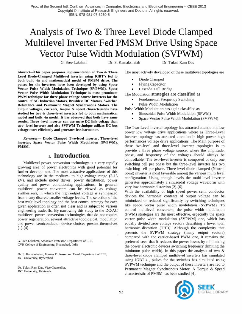
A. Two Level Diode Clamped Inverter The three phase two level voltage source diode clamped
inverter has shown in the Fig.1. It consists of six power (IGBT) switches. When the pulses are given to the switches the switches will conduct accordingly. When the positive IGBT is switched on (i.e) when the switches a, b or c is on then the corresponding lower IGBT will be in off state. Therefore by properly switching the IGBT’S we can get the
output voltage[10].
Fig.1. Three Phase Two-Level Diode Clamped Inverter
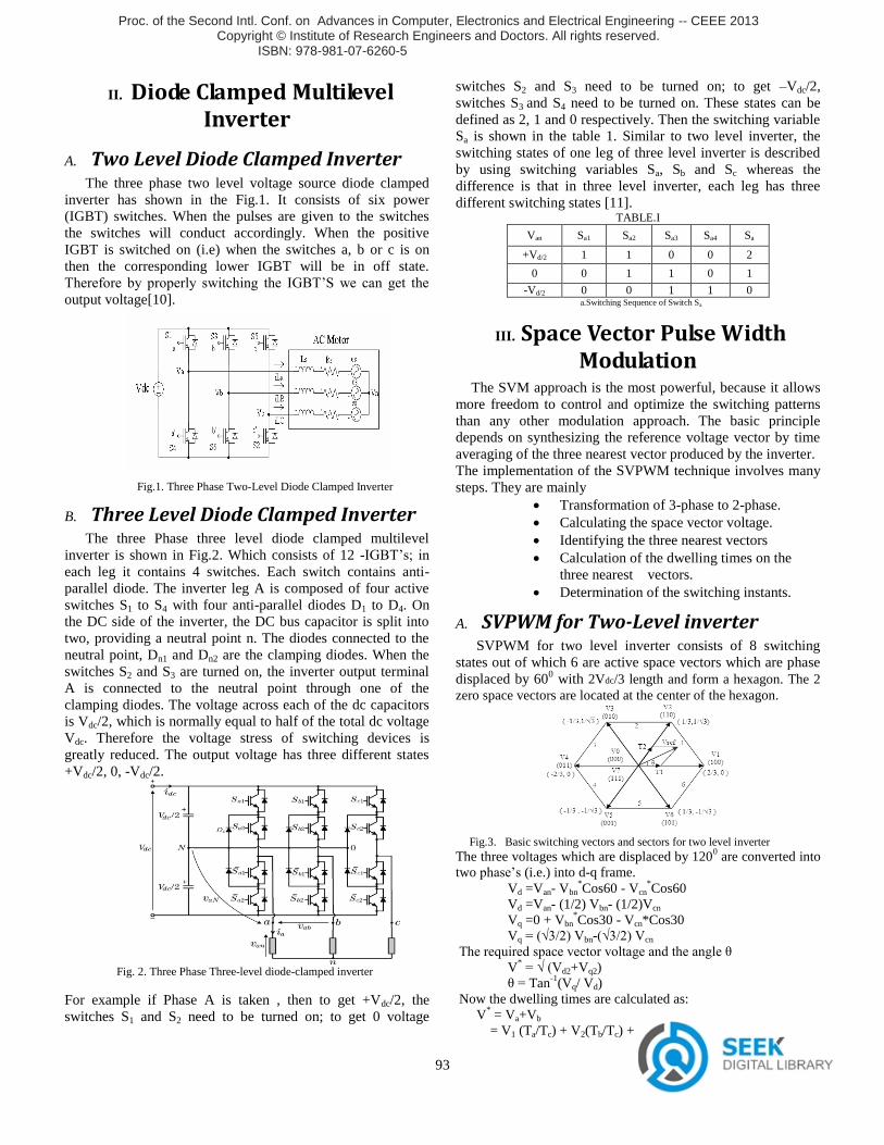
B. Three Level Diode Clamped Inverter The three Phase three level diode clamped multilevel
inverter is shown in Fig.2. Which consists of 12 -IGBT’s; in
each leg it contains 4 switches. Each switch contains anti-parallel diode. The inverter leg A is composed of four active switches S1 to S4 with four anti-parallel diodes D1 to D4. On the DC side of the inverter, the DC bus capacitor is split into two, providing a neutral point n. The diodes connected to the neutral point, Dn1 and Dn2 are the clamping diodes. When the switches S2 and S3 are turned on, the inverter output terminal A is connected to the neutral point through one of the clamping diodes. The voltage across each of the dc capacitors is Vdc/2, which is normally equal to half of the total dc voltage Vdc. Therefore the voltage stress of switching devices is greatly reduced. The output voltage has three different states +Vdc/2, 0, -Vdc/2.
Fig. 2. Three Phase Three-level diode-clamped inverter
For example if Phase A is taken , then to get +Vdc/2, the switches S1 and S2 need to be turned on; to get 0 voltage
switches S2 and S3 need to be turned on; to get –Vdc/2, switches S3 and S4 need to be turned on. These states can be defined as 2, 1 and 0 respectively. Then the switching variable Sa is shown in the table 1. Similar to two level inverter, the switching states of one leg of three level inverter is described by using switching variables Sa, Sb and Sc whereas the difference is that in three level inverter, each leg has three different switching states [11].
TABLE.I
Van Sa1 Sa2 Sa3 Sa4 Sa
+Vd/2 1 1 0 0 2
0 0 1 1 0 1
-Vd/2 0 0 1 1 0 a.Switching Sequence of Switch Sa
III. Space Vector Pulse Width Modulation
The SVM approach is the most powerful, because it allows more freedom to control and optimize the switching patterns than any other modulation approach. The basic principle depends on synthesizing the reference voltage vector by time averaging of the three nearest vector produced by the inverter. The implementation of the SVPWM technique involves many steps. They are mainly
Transformation of 3-phase to 2-phase. Calculating the space vector voltage. Identifying the three nearest vectors Calculation of the dwelling times on the
three nearest vectors. Determination of the switching instants.
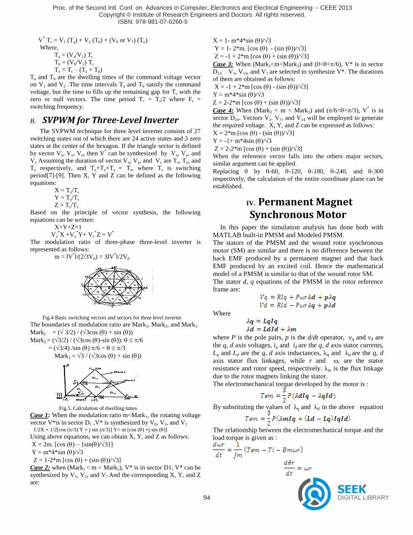
A. SVPWM for Two-Level inverter SVPWM for two level inverter consists of 8 switching
states out of which 6 are active space vectors which are phase displaced by 600 with 2Vdc/3 length and form a hexagon. The 2 zero space vectors are located at the center of the hexagon.
Fig.3. Basic switching vectors and sectors for two level inverter The three voltages which are displaced by 1200 are converted into two phase’s (i.e.) into d-q frame.
Vd =Van- Vbn*Cos60 - Vcn
*Cos60 Vd =Van- (1/2) Vbn- (1/2)Vcn Vq =0 + Vbn
*Cos30 - Vcn*Cos30 Vq = (√3/2) Vbn-(√3/2) Vcn
The required space vector voltage and the angle θ V* = √ (Vd2+Vq2) θ = Tan-1(Vq/ Vd) Now the dwelling times are calculated as: V* = Va+Vb = V1 (Ta/Tc) + V2(Tb/Tc) + (V0 or V7)(To/Tc).
Proc. of the Second Intl. Conf. on Advances in Computer, Electronics and Electrical Engineering -- CEEE 2013 Copyright © Institute of Research Engineers and Doctors. All rights reserved.
ISBN: 978-981-07-6260-5 doi:10.3850/ 978-981-07-6260-5_20
94
V* Tc = V1 (Ta) + V2 (Tb) + (V0 or V7) (To) Where, Ta = (Va/V1) Tc
Tb = (Vb/V2) Tc To = Tc – (Ta + Tb)
Ta and Tb are the dwelling times of the command voltage vector on V1 and V2 .The time intervals Ta and Tb satisfy the command voltage, but the time to fills up the remaining gap for Tc with the zero or null vectors. The time period Tc = Ts/2 where Fs = switching frequency.
B. SVPWM for Three-Level Inverter The SVPWM technique for three level inverter consists of 27
switching states out of which there are 24 active states and 3 zero states at the center of the hexagon. If the triangle sector is defined by vector Vx, Vy, Vz, then V* can be synthesized by Vx, Vy, and Vz Assuming the duration of vector Vx, Vy, and Vz are Tx, Ty, and Tz respectively, and Tx+Ty+Tz = Ts, where Ts is switching period[7]-[9]. Then X, Y and Z can be defined as the following equations: X = Tx/Ts Y = Ty/Ts Z = Tz/Ts Based on the principle of vector synthesis, the following equations can be written: X+Y+Z=1 Vx
*X +Vy*Y+ Vz
*Z = V* The modulation ratio of three-phase three-level inverter is represented as follows: m = lV*l/(2/3Vd) = 3lV*l/2Vd
Fig.4 Basic switching vectors and sectors for three level inverter The boundaries of modulation ratio are Mark1, Mark2, and Mark3 Mark1 = ( 3/2) / (3cos () + sin ()) Mark2 = (3/2) / (3cos ()-sin ()): /6
= (3/4) /sin () /6 < /3 Mark3 = 3 / (3cos () + sin ())
Fig.5. Calculation of dwelling times Case 1: When the modulation ratio m<Mark1, the rotating voltage vector V*is in sector D1 ,V* is synthesized by V0, V1, and V2 1/2X + 1/2[cos (/3) Y + j sin (/3)] Y= m [cos () +j sin ()] Using above equations, we can obtain X, Y, and Z as follows: X = 2m. [cos () – {sin()/3}] Y = m*4*sin ()/3 Z = 1-2*m [cos () + (sin ())/3] Case 2: when (Mark1 < m < Mark2), V* is in sector D1, V* can be synthesized by V1, V2, and V7 And the corresponding X, Y, and Z are:
X = 1- m*4*sin ()/3 Y = 1- 2*m. [cos () - (sin ())/3] Z = -1 + 2*m [cos () + (sin ())/3] Case 3: When (Mark2<m<Mark3) and (0<</6), V* is in sector D13 V1, V13, and V7 are selected to synthesize V*. The durations of them are obtained as follows: X = -1 + 2*m [cos () - (sin ())/3] Y = m*4*sin ()/3 Z = 2-2*m [cos () + (sin ())/3] Case 4: When (Mark2 < m < Mark3) and (/6<</3), V* is in sector D14. Vectors V2. V7, and V14 will be employed to generate the required voltage. X, Y, and Z can be expressed as follows: X = 2*m [cos () - (sin ())/3] Y = -1+ m*4sin ()/3 Z = 2-2*m [cos () + (sin ())/3] When the reference vector falls into the others major sectors, similar argument can be applied. Replacing by -60, -120, -180, -240, and -300 respectively, the calculation of the entire coordinate plane can be established.
IV. Permanent Magnet Synchronous Motor
In this paper the simulation analysis has done both with MATLAB built-in PMSM and Modeled PMSM. The stators of the PMSM and the wound rotor synchronous motor (SM) are similar and there is no difference between the back EMF produced by a permanent magnet and that back EMF produced by an excited coil. Hence the mathematical model of a PMSM is similar to that of the wound rotor SM. The stator d, q equations of the PMSM in the rotor reference frame are:
Where
where P is the pole pairs, p is the d/dt operator, νq and νd are the q, d axis voltages, iq and id are the q, d axis stator currents, Lq and Ld are the q, d axis inductances, λq and λd are the q, d axis stator flux linkages, while r and ωr are the stator resistance and rotor speed, respectively. λm is the flux linkage due to the rotor magnets linking the stator. The electromechanical torque developed by the motor is :
By substituting the values of λq and λd in the above equation
The relationship between the electromechanical torque and the load torque is given as :
Proc. of the Second Intl. Conf. on Advances in Computer, Electronics and Electrical Engineering -- CEEE 2013 Copyright © Institute of Research Engineers and Doctors. All rights reserved.
ISBN: 978-981-07-6260-5 doi:10.3850/ 978-981-07-6260-5_20
95
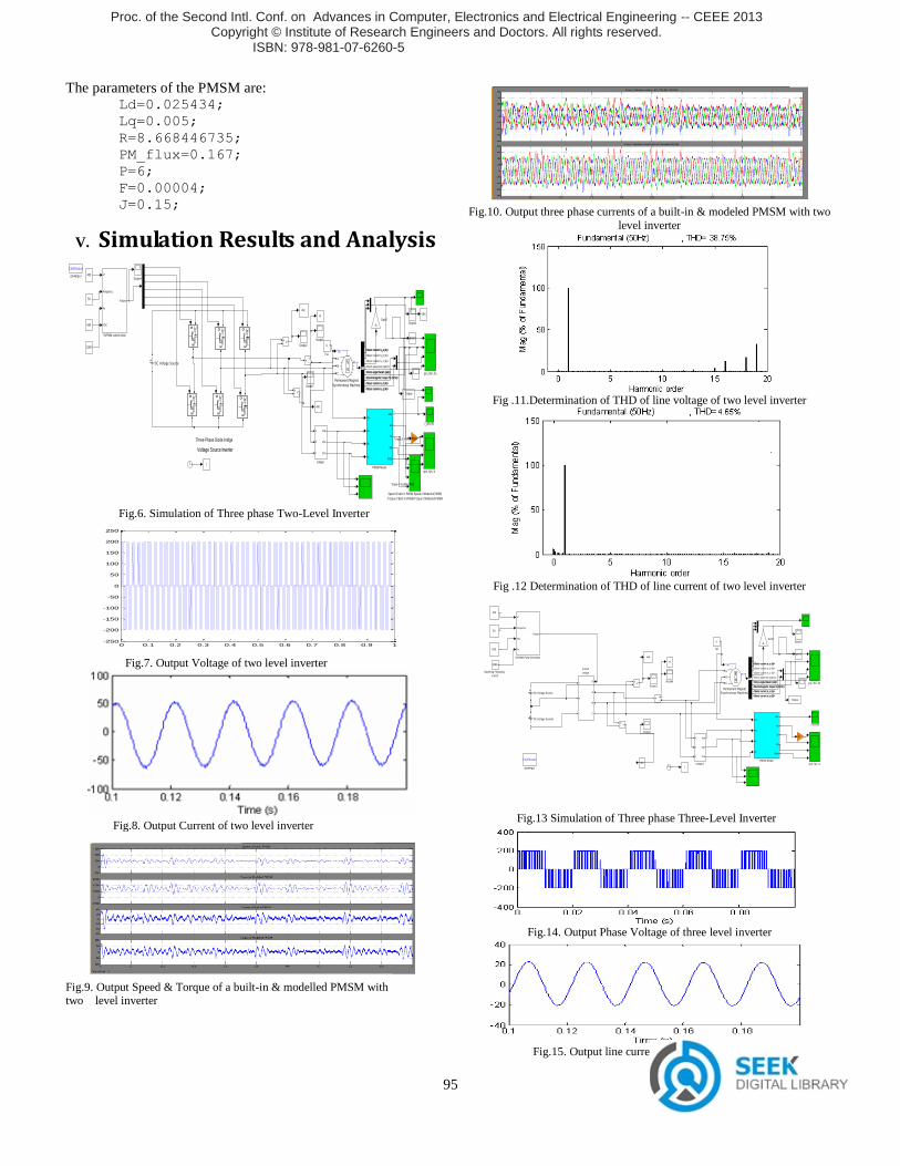
The parameters of the PMSM are: Ld=0.025434; Lq=0.005; R=8.668446735; PM_flux=0.167; P=6; F=0.00004; J=0.15;
V. Simulation Results and Analysis
Three-Phase Diode bridge
Voltage Source Inverter
i_abc (A)
rpm, Nm, A1
rpm, Nm, A
Continuous
powergui
Vab
Vbc
Vca
A
B
C
outage
v+-
v+- 4
Ts1
iabc
Torque
speed
vab
vbc
ia
t
Speed of built in PMSM,Speed of Modelled PMSM
,Torque of Built in PMSM,Torque of Modelled PMSM
Scope7
Scope6
Scope4
Scope2
Scope1
V*
Frequency
Fs
VDC
Pulses
SVPWM control block
Tm
mA
B
C
Permanent MagnetSynchronous Machine
Tm
Va
Vb
Vc
iabc
we
Te
idq
theta
PMSM Model
g CE
g CE
g CE
g CE
g CE
g CE
-K-
Gain7
DC Voltage Sourcei
+-
1080
600
50
400
-K-
Torque of modeld PMSM
Torque of modeld PMSM
<Stator current is_a (A)><Stator current is_a (A)>
<Stator current is_b (A)>
<Stator current is_c (A)>
<Rotor speed wm (rad/s)>
<Electromagnetic torque Te (N*m)><Electromagnetic torque Te (N*m)>
<Rotor angle thetam (rad)><Rotor angle thetam (rad)>
<Stator current is_d (A)><Stator current is_d (A)>
<Stator current is_q (A)><Stator current is_q (A)>
Fig.6. Simulation of Three phase Two-Level Inverter
0 0.1 0.2 0.3 0.4 0.5 0.6 0.7 0.8 0.9 1-250
-200
-150
-100
-50
0
50
100
150
200
250
Fig.7. Output Voltage of two level inverter
Fig.8. Output Current of two level inverter
Fig.9. Output Speed & Torque of a built-in & modelled PMSM with two level inverter
Fig.10. Output three phase currents of a built-in & modeled PMSM with two
level inverter
Fig .11.Determination of THD of line voltage of two level inverter
Fig .12 Determination of THD of line current of two level inverter
i_abc (A)
rpm, Nm, A1
rpm, Nm, A
Continuous
powergui
Vab
Vbc
Vca
A
B
C
outage1
v+-
v+-
4
Ts1
Torque
speed
vab
van
ia
t
1080
Switching Frequency
in KHZ
Scope7
Scope6
Scope2
Scope1
V*
Frequency
Vdc
Fs
Pulses
SVPWM Pulse Generator
Tm
mA
B
C
Permanent MagnetSynchronous Machine1
Tm
Va
Vb
Vc
iabc
we
Te
idq
theta
PMSM Model
-K-
Gain7
DC Voltage Source1
DC Voltage Source
i+
-
600
50
400
G
A
B
C
+
N
-
3-level
bridge
-K-
<Stator current is_a (A)><Stator current is_a (A)>
<Stator current is_b (A)>
<Stator current is_c (A)>
<Rotor speed wm (rad/s)>
<Electromagnetic torque Te (N*m)><Electromagnetic torque Te (N*m)>
<Rotor angle thetam (rad)><Rotor angle thetam (rad)>
<Stator current is_d (A)><Stator current is_d (A)>
<Stator current is_q (A)><Stator current is_q (A)>
Fig.13 Simulation of Three phase Three-Level Inverter
Fig.14. Output Phase Voltage of three level inverter
Fig.15. Output line current of three level inverter
Proc. of the Second Intl. Conf. on Advances in Computer, Electronics and Electrical Engineering -- CEEE 2013 Copyright © Institute of Research Engineers and Doctors. All rights reserved.
ISBN: 978-981-07-6260-5 doi:10.3850/ 978-981-07-6260-5_20

96
Fig.16. Output Line Voltage of three level inverter
Fig.17 Output Speed & Torque of a built-in & modelled PMSM with three
level inverter
Fig.18 Output three phase currents of a built-in & modeled PMSM with three
level inverter
Fig .19.Determination of THD of line voltage of three level inverter
Fig .20. Determination of THD of line current of three level inverter
VI. Conclusion In this paper, Two & Three level diode clamped inverters are simulated using IGBT’s. The Pulses for the switches has
developed using Space Vector Pulse Width Modulation Technique. The Outputs of the inverters are fed to the Permanent Magnet Synchronous Motor for two types one is built in model and the other is simulated model. Simulation analyses concerning the applications of SVPWM control strategy on the two and three level diode clamped IGBT’s inverters Fed PMSM drive are presented. The output Voltages of Two Level & Three Level inverters and the Torque, Speed characteristics of PMSM drive has been studied. From this analysis author can conclude that multilevel inverter can eliminate the harmonics produced by the normal inverter. It has been observed that three level inverter gives good performance characteristics than two level inverter. The output Torque, Speed has been improved using three level diode clamped inverter. From the results it is concluded that three level inverter can use more dc link voltage than two level inverter and also SVPWM Technique utilizes DC bus voltage more efficiently and generates less harmonics. Also it has been observed that the torque, speed and three phase currents of both built-in & modeled PMSM drive have same waveforms.
References [1] Aneesh, M.A.S., Gopinath.A, Baiju.M.R. ” A Simple Space Vector
PWM Generation Scheme for Any General n-Level Inverter “Vol.56, issue-5, Industrial Electronics, IEEE Transactions, pp.1649-1656, May-2009
[2] Gupta.G.K, Khambadkone.A.M.,” A Space Vector PWM Scheme for Multilevel Inverters Based on Two-Level Space Vector PWM “ vol.53, issue-5,Industrial Electronics, IEEE Transactions,Oct.2006
[3] “Pulse width modulation for power converters” principles and practice by D. Grahame Holmes and Thomas A. L
[4] “Multilevel inverters: a survey of topologies, controls, and applications” by José Rodríguez, Jih-Sheng Lai, and Fang Zheng Peng 1999 IEEE paper.
[5] Multilevel converters for large electric drives” by Leon M. Tolbert, Fang Zheng Peng, and Thomas G. Habetler.
[6] “Fault diagnosis system for a multilevel inverter using a neural network” by Surin Khomfoi & Leon M. Tolbert.
[7] “A simple svpwm algorithm for multilevel inverters” by Lei Hu, Honyan Wang, Yan Deng and Xiangning He College of Electrical Engineering, Zhejiang University Hang Zhou, China. 2004 35th Annual IEEE Power Electronics Specialists Conference.
[8] Jae Hyeong Seo, Chang Ho Choi, Dong Seok Hyun “A new simplified space-vector PWM method for three-level inverters “Vol.16, issue-4, Powerelectronics IEEE Transcations, pp..545-550, july-2001.
[9] Reney.D, “Modeling and Simulation of Space Vector PWM Inverter “, Devices and Communications (ICDeCom), International Conference, pp.1- 4, 24-25th feb,2011.
[10] Lwwicki.A, Krzeminski.Z, Abu-Rub.H. “Space-Vector Pulsewidth Modulation for Three-Level NPC Converter With the Neutral Point Voltage Control “ Vol.58, issue-11, pp.5076-5086,Industrial Electronics, IEEE Transactions, Nov.2011.
[11] Lourci.N, Berkouk.E.M., Boudiema.F., Petzoldt.J. Dali.M.Y., “A simplified space vector pulse width modulation algorithm for five level diode clamping inverter “ pp.1349-1354, Power Electronics Electrical Drives,SPEEDAM,23-26th May,2006.
Proc. of the Second Intl. Conf. on Advances in Computer, Electronics and Electrical Engineering -- CEEE 2013 Copyright © Institute of Research Engineers and Doctors. All rights reserved.
ISBN: 978-981-07-6260-5 doi:10.3850/ 978-981-07-6260-5_20