analytical and numerical modeling of organic photovoltaic devices
TRANSCRIPT

McMaster UniversityDigitalCommons@McMaster
Open Access Dissertations and Theses Open Dissertations and Theses
9-1-2010
Analytical And Numerical Modeling Of OrganicPhotovoltaic DevicesMohammad Jahed Tajik
Follow this and additional works at: http://digitalcommons.mcmaster.ca/opendissertationsPart of the Electrical and Computer Engineering Commons
This Thesis is brought to you for free and open access by the Open Dissertations and Theses at DigitalCommons@McMaster. It has been accepted forinclusion in Open Access Dissertations and Theses by an authorized administrator of DigitalCommons@McMaster. For more information, pleasecontact [email protected].
Recommended CitationTajik, Mohammad Jahed, "Analytical And Numerical Modeling Of Organic Photovoltaic Devices" (2010). Open Access Dissertationsand Theses. Paper 4272.

ANALYTICAL AND NUMERICAL
J\IODELING OF ORGANIC
PHOTOVOLTAIC DEVICES

ANALYTICAL AND NUMERICAL MODELING OF
ORGANIC PHOTOVOLTAIC DEVICES
BY
MOHAMMAD JAHED TAJIK
Master's of Applied Science
Sharif University of Technology
A THESIS SUBMITTED TO THE SCHOOL OF GRADUATE STUDIES IN PARTIAL FULFILLMENT OF THE
REQUIREMENTS FOR THE DEGREE OF MASTER'S OF SCIENCE
McMaster University Hamilton, Ontario, Canada
© Copyright by Mohammad Jahed Tajik, September 2010

MASTER OF APPLIED SCIENCE (2010) (Electrical and Computer Engineering)
McMaster University Hamilton, Ontario
TITLE:
AUTHOR:
SUPERVISORS: NUMBER OF PAGES:
Analytical And Numerical Modeling Of Organic
Photovoltaic Devices
Mohammad J ahed Tajik, Master's of Science
(Sharif University of Technology)
Prof. M. Jamal Deen and Prof. W. Ross Datars LXXXIX, 89
ii

Abstract The energy crises, along with the recent global warming trends, demand an immediate cut in the use of fossil fuel. Therefore, renewable sources of energy and especially solar power, have
gained tremendous attention from the consumer countries as a possible candidate to replace the carbon-based energy supplies. Among all different types of solar cells, flexibility, cost-effective fabrication processes, combined with low-price materials and most importantly a great potential
for improvement make organic solar cells an interesting topic for research. On the other hand,
modeling provides a valuable opportunity to study device properties that experimentally are out of reach, expensive or need a long time to measure. These mentioned reasons motivated us to
choose modeling of organic solar cells as the subject of our research.
In this research, we tried to provide a complete study of the power generating procedure in
organic solar cells by modeling all of the following processes: in-coupling of the photons,
absorption of the photons, formation of the excitons, diffusion of the excitons, dissociation of the excitons, transportation of the charges and collection of the charges at the electrodes.
To get a better understanding and also because of basic physical differences, the modeling is divided into two parts: the optical section and the electrical section. Each section is also divided
into two separate segments, analytical and numerical analysis.
Using the optical models with different designs to improve the performance of the solar cells, the
effect of the layer thickness and two- and three-dimensional light focusing apertures on the intensity oflight at the junction ofn-type and p-type materials (for bilayer heterojunction organic solar cells) are studied. Results show that for a certain design of the light focusing aperture, a 98% increase in the light absorption in a bilayer heterojunction solar cell can be obtained.
The electrical performance of organic solar cell is also studied by using analytical modeling of
exciton diffusion for bilayer heterojunction solar cells and numerical models based on driftdiffusion procedures by using COMSOL multiphysics software for bulk heterojunction solar
cells. Based on the mismatch between the calculated results and measurement (counterdiode
effect), a tunneling current correction is introduced. Finally, using the tunneling current model, the energy diagram ofthe organic active layer at the metallic contact is characterised.
In summary, five different models are described in five separate sections, and at the end of each
section, results are reported and compared with the literature that prove that the presented models
can be used for a new design of organic solar cell characteristics to improve the performance of the device. Also, by introducing the tunneling current to model the counterdiode effect, we have
contributed to the literature.
111

Acknowledgements I would like to start by his mane the compassionate the merciful that all good things start with his
name. Next, I would like to express my sincere gratitude to my supervisors, Prof. M. Jamal
Deen and Prof. Ross W. Datars, for giving me the opportunity to work on this subject and for
their continuous support and guidance throughout my work. It is indeed an honour to have the
opportunity to follow into the footsteps of such a great mentors. I have learned, and I continue to
learn so much from them and I hope that my future achievements meet and exceed the
expectations of being one of their students.
I would also like to thank my good friends and colleagues in the Microelectronics research
Laboratory, Mohammad Reza Dadkhah, Mohammad Wa1eed Shinwari, Salman Safari, Munir M.
EI-Desouki, Darek Palubiak, Dr. Ognian Marinov, Dr. Mehdi Kazemeini and especially Mr.
Hossein Kassiri Bidhendi and his lovely wife "Maryam" and also Mohammad Hassan Sobhani
and his lovely wife "Vista", Dr. Peyman Setoodeh and everybody else whom I have forgot to
mention, for their sincere friendship and supports.
I would like to thank Prof. Xun Li and Dr. Shiva Kumar for taking the time to review my thesis
and for being in my committee. I would also like to thank other faculty members at McMaster
University, such as Dr. Yaser M. Haddara, Dr. Chin-Hung Chen, Dr. A. Patriciu, Dr. S. Shirani,
Also, not forgetting the administrative staff at the ECE department, especially Cheryl Gies, Terry
Greenlay, Cosmin Coroiu, Helen Jachna and Steve Spencer.
And of course, I wish to thank my family for their limitless love, support, and encouragement.
They will be in my heart for ever and I couldn't miss them anymore.
iv

List of Contents ABSTRACT .................................................................................................................................. iii
ACKNOWLEDGEMENTS ........................................................................................................ iv
LIST OF CONTENTS .................................................................................................................. v
LIST OF TABLES ...................................................................................................................... !. x
LIST OF SYMBOLS AND ACRONYMS ................................................................................. xi
1. INTRODUCTION ................................................................................................................. 1
1.1. PHOTOVOLTAIC OVER THE PASSAGE OF TIME ......................................................... 2
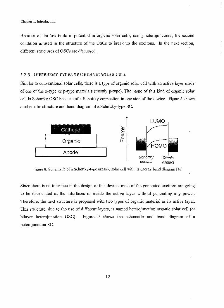
1.2. ORGANIC SOLAR CELLS ..................................................................................................... 6 1.2.1. WHY ORGANIC SOLAR CELL? ........................................................................................................ 6 1.2.2. DIFFERENCES BETWEEN ORGANIC AND INORGANIC SOLAR CELLS .............................. : ... 7 1.2.3. DIFFERENT TYPES OF ORGANIC SOLAR CELL ......................................................................... 12
1.3. ORGANIZATION OF THE THESIS .................................................................................... 15
OPTICAL MODELING ............................................................................................................. 18
2. OPTICAL MODELING ..................................................................................................... 18
2.1. OPTICAL MODEL, ANALYTICAL ANALYSIS ............................................................... 20 2.1.1. TRANSFER MATRIX METHOD (TM) ............................................................................................. 20
2.1.1.1. Description of the TM Model. .................................................................................................... 20 2.1.1.2. TM Model, Results and Discussion ............................................................................................ 25
2.2. OPTICAL MODEL, NUMERICAL ANALYSIS ................................................................. 31 2.2.1. TWO DIMENSIONAL OPTICAL MODEL ....................................................................................... 32
2.2.1.1. Description of the Two Dimensional Model .............................................................................. 32 2.2.1.2. Two Dimensional Model, Results and Discussion ..................................................................... 36
2.2.2. THREE DIMENSIONAL OPTICAL MODEL .................................................................................. .43 2.2.2.1. Description of the Three Dimensional Model .......................................................................... A4 2.2.2.2. Three Dimensional Model, Results and Discussion .................................................................. .49
3. ELECTRICAL MODELING ............................................................................................ 55
3.1. ELECTRICAL MODEL, ANALYTICAL ANALYSES ...................................................... 57 3.1.1. EXCITON DIFFUSION EQUATION ................................................................................................. 57
3.1.1.1. Description of the Exciton Diffusion Model .............................................................................. 57 3.1.1.2. Exciton Diffusion Equation Results and Discussion: ................................................................. 60
3.2. NUMERICAL ANALYSIS, ELECTRICAL MODEL ........................................................ 61 3.2.1. DRIFT-DIFFUSION MODEL ............................................................................................................. 62
3.2.1.1. Description of the Drift-Diffusion Model .................................................................................. 62 3.2.1.2. Drift-Diffusion Model, Results and Discussion ......................................................................... 72
3.3. THE CORRECTION OF ELECTRICAL MODEL USING TUNNELING CURRENT. 74
v

4. CONCLUSION AND RECOMMENDATION FOR FUTURE WORK ....................... 83
4.1. CONCLUSION ........................................................................................................................ 83
4.2. RECOMMENDATION ........................................................................................................... 84
REFERENCES ............................................................................................................................ 86
VI

List of Figures Figure 1: Forecast of electrical power cost, supply, demand and cost of solar PV electricity for different technologies [3]. ........... 2
Figure 2: Best research cell efficiencies from 1975 up to now [4] .................................................................................................... 5
Figure 3: A reel to reel printing machine in CSIRO institution, Australia [6] ............................................................................... _ ... 7
Figure 4: Chemical structure of two organic materials that are usually used in DSSCs [16] ............................................................ 8
Figure 5: Chemical structure of some of the famous molecules that are used in OSCs [16] ............................................................. 9
Figure 6: Chemical structures of some of the famous polymers that are used in OSCs [16] .......................................................... 10
Figure 7: Schematic of a inorganic SC (left) and an organic heterojunction SC (right) [18] .......................................................... 11
Figure 8: Schematic of a Schottky-type organic solar cell with its energy band diagram [16] ....................................................... 12
Figure 9: Schematic ofa heterojunction organic solar cell with its energy band diagram [16] ...................................................... 13
Figure 10: Principle of exciton dissociation and charge separation in a heterojunction organic solar cell [17] ............................. 13
Figure 11: A very rudimentary illustration of bulk heterojunction SC and a bilayer heterojunction SC [18]. ................................ 14
Figure 12: Schematic of the band structure in bulk heterojunction solar cell [19]. ......................................................................... 15
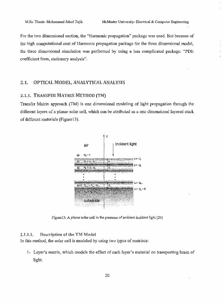
Figure13: A planar solar cell in the presence of ambient incident light [20] .................................................................................. 20
Figure 14: Demonstration of the layer and interface matrices, the left side is the interface of two layers and the picture on the right side shows the propagation oflight inside a layer [16] ........................................................................................................... 21
Figure 15: The active layers interface ............................................................................................................................................. 24
Figure 16: Refractive indices as a function of wavelength. For the following material with their references Al refractive indices [34], PEOPT refractive indices [35], PtEOP refractive indices [36], C60 refractive indices [37], ITO refractive indices [38] ...... 26
Figure 17: Pattern of the electromagnetic wave amplitude in the six layer solar cell for ),,=470nm: (A) shows the pattern for a device for C60 layer thickness equal to 35nm, (B) shows the situation for a 80nm thick C60 layer .............................................. 27
Figure 18: Amplitude of the electromagnetic wave at the active area interface for a 60nm thick PEPOT layer and 60 different thicknesses of C60 layer, ranging from 5nm to 300nm. The result is compared the literature [28]. ............................................... 28
Figure 19: The second device configuration (shown below) and the refractive index of the polymer [poly(2,7-(9-(2'-ethylhexyl)-9-hexylfluorene)- alt-5,5-(4',7' -di-2thienyl-2',1 ' ,3'-benzothiadiazole))] [31] ............................................................................... 29
Figure 20: Light absorption as a function of polymer thickness and C60 thickness. The thickness ofPedot:PSS is 100nm and of ITO 120 nm .................................................................................................................................................................................... 30
Figure 21: Accessing the Harmonic propagation package at the opening window of the COMSOL Multiphysics ........................ 32
Figure 22: Meshing of a planar solar cell via adaptive meshing .................................................................................................... _. 33
Figure 23: Spectrum of the sun (left) [32], Solar spectrum given to COMSOL (right) .................................................................. 34
Figure 24: Subdomain settings for the Harmonic propagation package .......................................................................................... 35
Figure 25: Comparison ofTM and COMSOL results ..................................................................................................................... 37
Figure 26: Some capping structure and their effect on profile oflight on the device ...................................................................... 38
vii

Figure 27: Three dimensional equivalent geometries of the modeled solar cells with three different forms of light trapping structure at the first layer ................................................................................................................................................................ 38
Figure 28: The intensity of light at the interface of C60 and PEOPT for wavelength between 300nm to 700nm, using triangular arrays at the first layer. ................................................................................................................................................................... 39
Figure 29: The intensity of light at the interface of C60 and PEOPT for wavelength between 300nm to 700nm, using rectangular arrays at the first layer. ................................................................................................................................................................. .-. 40
Figure 30: The intensity of light at the interface of C60 and PEOPT for wavelength between 300nm to 700nm, using semicircular arrays at the first layer .................................................................................................................................................................... 41
Figure 31:Meshing in COMSOL in two and three dimensions ....................................................................................................... 43
Figure 32: Stationary analysis ofPDE coefficient form of classical PDEs package ....................................................................... 45
Figure 33: results of a simple three dimensional two layered structure .......................................................................................... 49
Figure 34: Quantum well and a structure with different refractive indiceses .................................................................................. 50
Figure 35: Three different light focusing first layer structure: cones, semisphere and blocks ........................................................ 50
Figure 36: Concept of mirror boundary condition with a real source of light in the middle and two imaginary sources of light in its right and left. (imaginary rays are represented by doted lines) ................................................................................................... 51
Figure 37: The intensity of light at the interface of C60 and PEOPT for wavelengths between 325nm and 700nm, using blocks at the first layer. .................................................................................................................................................................................. 52
Figure 38: The intensity of light at the interface of C60 and PEOPT for wavelengths between 300nm and 700nm, using cones at the first layer. ................................................................................................................................................................................. -. 52
Figure 39: The intensity of light at the interface of C60 and PEOPT for wavelengths between 300nm and 700nm, using spheres at the first layer ................................................................................................................................................................................... 53
Figure 40: The structure of the solar cell that has been modeled in this section [28]. ..................................................................... 60
Figure 41: The IPCE (Incident monochromatic Photon to Current collection Efficiency) calculated for the first solar cell compared to the experimental result reported in [28] ..................................................................................................................... 61
Figure 42: The band diagram of a bulk heterojunction OSC .......................................................................................................... 63
Figure 43: Depiction of the Poisson equation package root in the first window of the COMSOL simulator for the one dimensional model. ............................................................................................................................................................................................. 65
Figure 44: Flowchart of the electrical model. ................................................................................................................................. 66
Figure 45: Picture of Steady-state analysis of convection and diffusion at the opening window of COMSOL. ............................. 68
Figure 46: Comparison of my COMSOL simulation and simulation results from [41]. The curves with (+, ., I'l) are the result of my simulation and the ones with (I'l, 0, D) at the background are the result of Glatthaar & et. al. [41]. The parameters for both of the cases are demonstrated in Table 9 ............................................................................................................................................. 72
Figure 47: Measurement result ofI-V curve from [41] (left) compared to the numerical results (right) ........................................ 73
Figure 48: I -V curve of a diode, a current source and their parallel combination that makes a solar cell. ...................................... 74
Figure 49: The result of an ordinary solar cell and a parallel diode which will result into a I-V curve of a device similar to a BR-OSC by including the effect of tunneling current (the counterdiode effect) ................................................................................... 74
Figure 50: Difference in the band diagram of the solar cell with (Right) and without taking the counterdiode effect into account (Left) ............................................................................................................................................................................................... 76
V11l

Figure 51: Band diagram of a solar cell for different biasing and the direction of the current. Blue arrows stand for the direction of the carrier due to the thermionic emission and the red arrows show the direction of electron tunneling the barrier at the interface (at the left). The experimental result from [41] with separated region in the bias for each one of the four conditions at the left ............................................................................................................................................................................................. 77
Figure 52: The difference between the experimental I-V curve and numerical result that are shown in Figure 47 ........................ 79
Figure 53: Modified tunneling current for three different barrier widths (3nm, 7nm and lOnm) with forty different barrier heights from leV to 2eV. The direction of the red arrows in the pictures indicates the increase in the barrier height... ............................. 80
Figure 54: Comparison of calculated I-V corrected by tunneling current (circles) with measurement results reported by Glatthaar et. al. [41] (triangles) ...................................................................................................................................................................... 81
IX

List of tables Table I: Boundary conditions for the Hannonic propagation package ........................................................................................... 35
Table 2: Results of the simulation for the focusing apertures nonnalized to the flat surface results ............................................... 42
Table 3: The Plethora of equations that can be modeled via PDE coefficient fonn (stationary analysis) ....................................... 46
Table 4: Parameters values for generating Helmholtz's equation ................................................................................................... 46
Table 5: General boundary conditions, for electromagnetic waves ................................................................................................ 47
Table 6: Choosing of parameters to generate the needed boundary conditions .............................................................................. 48
Table 7: Results of the simulation for the focusing apertures nonnalized to the flat surface results ............................................... 54
Table 8: Reported parameters of ITO ............................................................................................................................................. 56
Table 9: Parameters that have been used in Figure 46 .................................................................................................................... 70
Table 10: Parameters that are used in Figure 54 ............................................................................................................................. 81
x

List of Symbols and Acronyms Symbols
E/
r
M
I
L
M'
M"
S
B
Q(z, OJ)
n
/lp
G
R
Ndopillg
Transmitted ray
Reflected ray
Fresnel complex transmission coefficients
Fresnel complex reflection coefficients
The transfer matrix
The interface matrices
The layer's matrix
The prim-system
The bis-system
Poynting's vector
The magnetic field
Dissipated power at point z and frequency OJ
Refractive Indices
Exciton's exchange efficiency
The diffusion constant
Inverse of the exciton's diffusion length
Exchange rate
Wavelength
Calculated photocurrent
Electron's mobility
Hole's mobility
Generation rate
Recombination rate
Applied voltage
Bandgap
Dopants' density
Xl

fit
X
Pinit
Jtllllllelling
Acronyms
PV
SC
OSC
OPV
CSIRO
ODSSC
DSSC
BHJOSC
LUMO
HOMO
TM
IPCE
Intrinsic carrier density
Thermal voltage
Electron affinity
Initial hole concentration at the interfaces ofthe active layer
Initial electron concentration at the interfaces of the active layer
Work function
Location ofthe organic layer's LUMO
Effective mass ofthe electron inside the metallic electrode
Effective mass of electron inside the dielectric
Width of the barrier layer
Electrical filed inside of the barrier
Tunneling current
Photovoltaic
Solar cell
Organic solar cell
Organic photovoltaic
Commonwealth Scientific and Industrial Research Organisation
Organic dye-sensitized solar cell
Dye-sensitized solar cell
Bulk heterojunction solar cell
Lowest unoccupied molecular orbital
Highest occupied molecular orbital
Transfer matrix
Incident monochromatic photon to current collection efficiency
XlI
FEM
FDTD
PFDTBT
ITO
TE
AM 1.5
ASTM
P3HT
PCBM
lD
LED
FF
Finite element method
Finite-Difference Time-Domain
Polymer [poly(2,7-(9-(2' -ethylhexyl)-9-hexylfluorene)- alt-5,5-( 4',7' -di-2 thienyl-
2', I' ,3'-benzothiadiazole))]
Indium thin oxide
Transversal electric polarization
Airmass
American Society for Testing and Materials
Poly(3-hexylthiophene)
[6,6]-phenyl C61-butyric acid methyl ester
One-dimensional
Light emitting diode
Fill Factor
X111


M.Ss. Thesis- Mohammad Jahed Tajik McMaster University- Electrical & Computer Engineering
CHAPTER 1
INTRODUCTION
1. INTRODUCTION
Energy crises, global warming, emission of greenhouse gases (water vapor, carbon dioxide,
methane, nitrous oxide, etc.) are known to be the origin of one of the greatest threats for the
future of life on earth. Also, the energy crisis, fragile markets due to the present economic
recession as well as the insecure and unstable future of oil and gas production prospect
encourage the consumers to search for and develop more stable and possibly less expensive new
sources of energy.
Among all of the renewable resources, Photovoltaic (PV) energy seems to be one of the most
promising and secure fields that can be adopted by the majority of the countries around the world
as a safe and clean substitute for their existing fossil fuel power plants. As the records show [1],
PV has the fastest growing rate among renewable energy sources and is actually one of the
fastest growing industries among all of the green energies. Most of the growth (40% per year [2])
is in the crystalline silicon technology and the rest is divided between amorphous semiconductor
based solar cells (SCs), thin film SCs, dye sensitized SCs, organic solar cells (OSCs) and other
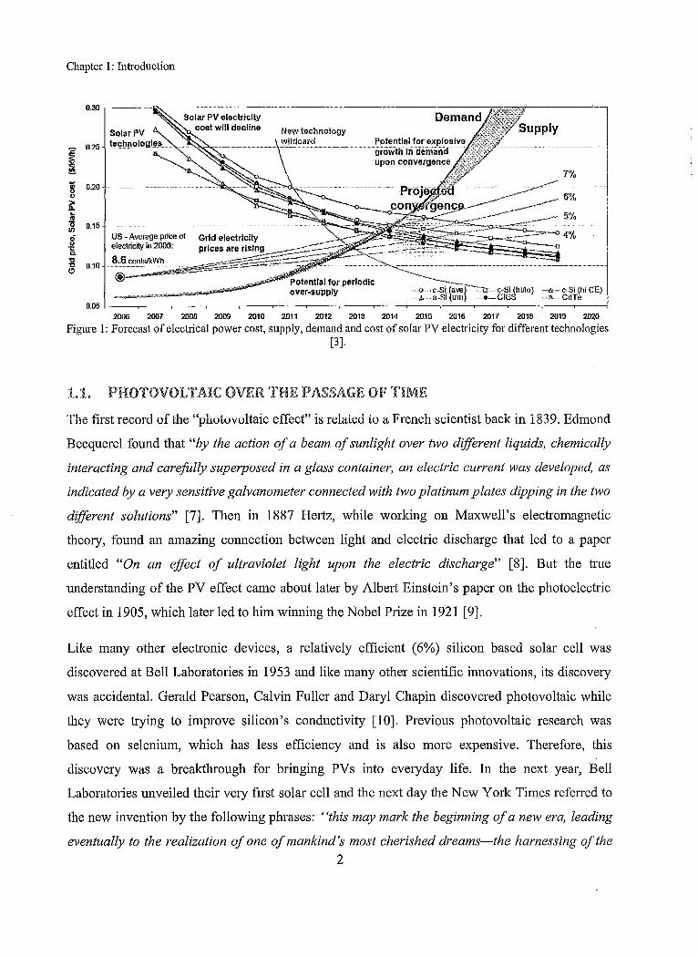
SCs. Figure 1 shows the forecast of the demand, supply and the estimated cost of electrical
power and photo electrical power for the next ten years in the US energy market. As can be seen
in the picture, solar power cannot be a competitive source of power any sooner than 2015 and by
the end of2019 it will be even cheaper than the most pessimistic estimate of the price of energy.
1
Chapter 1: Introduction
O~,··------~--------------------------------------------~
2 025
~ ~ 7% ..
020 ~ ... ~.-... ---~-.-... -.-
IJ
it 6%
.!i 0 0.15 Ul
CIi US - Average price of
i! electricity in 2006: ... :g 0.10
8.6 cen1slkWh (!)
---6- c-Si (hi GEl -n-GdTe
0.05 2006 2007 2OIJ8 2009 2010 2011 2012 2013 2014 2015 2016 2017 2018 2019 2020
Figure I: Forecast of electrical power cost, supply, demand and cost of solar PV electricity for different technologies [3].
1.1. PHOTOVOLTAIC OVER THE PASSAGE OF TIME
The first record of the "photovoltaic effect" is related to a French scientist back in 1839. Edmond
Becquerel found that "by the action of a beam of sunlight over two different liquids, chemically
interacting and carefully superposed in a glass container, an electric current was developed, as
indicated by a very sensitive galvanometer connected with two platinum plates dipping in the tyvo
different solutions" [7]. Then in 1887 Hertz, while working on Maxwell's electromagnetic
theory, found an amazing connection between light and electric discharge that led to a paper
entitled "On an effect of ultraviolet light upon the electric discharge" [8]. But the tme
understanding of the PV effect came about later by Albert Einstein's paper on the photoelectric
effect in 1905, which later led to him winning the Nobel Prize in 1921 [9].
Like many other electronic devices, a relatively efficient (6%) silicon based solar cell was
discovered at Bell Laboratories in 1953 and like many other scientific innovations, its discovery
was accidental. Gerald Pearson, Calvin Fuller and Daryl Chapin discovered photovoltaic while
they were trying to improve silicon's conductivity [10]. Previous photovoltaic research was
based on selenium, which has less efficiency and is also more expensive. Therefore, this
discovery was a breakthrough for bringing PVs into everyday life. In the next year, Bell
Laboratories unveiled their very first solar cell and the next day the New York Times referred to
the new invention by the following phrases: "this may mark the beginning of a new era, leading
eventually to the realization of one of mankind's most cherished dreams-the harnessing of the 2

M.Ss. Thesis- Mohammad Jahed Tajik McMaster University- Electrical & Computer Engineering
almost limitless energy of the sun for the uses of civilization. }} It sure has an immense effect on
the civilization, but it took more than half a century for solar cell to actually become a
comparable opponent for the existing carbon based energy supplies.
Later in 1955, the United States' government announced that they had a plan to launch satellites.
Because of the impossibility of providing power to the satellite from earth, there was a good
opportunity for PV s to show their value. Therefore, suddenly there was an application with a
wealthy sponsor to support the research on PV s. Most of the later innovations and development
in the solar power field happened in the Cold War years and during the adversary between Soviet
Union and United States over control of space, or in a better word in the famous "Space Race".
The next applications for SCs apart from the space application were related to oil rigs in the Gulf
of Mexico. For security reasons it is needed for tall structures to have a blinking light on them,
but once again the distance to the source of electricity made this the next job of SCs.
Time passed by for solar cell to find its place in history, but it was still far away from the house's
roof. To become compatible with other electrical sources and to become a domestic power
source, two major improvements had to happen, for the solar cells:
1- The size of each unit should shrink (improvement in efficiency)
2- The cost of manufacturing should have been reduced to improve the ratio of costlk-watt
To improve the efficiency, the quality of the materials had to be improved (better crystal
quality), fabrication methods had to be reformed and new structures had to be introduced (i.e.
two and three stag solar cells). However, all of the mentioned changes would increase the cost of
manufacturing. Therefore, at the same time, researchers were trying to make the total cost of the
solar cells decrease by finding cheaper types of material (i.e. amorphous semiconductors, organic
material and so on) or cheaper structures with lower manufacturing cost (i.e. planar SCs with
printing technique as their fabrication method [5]).
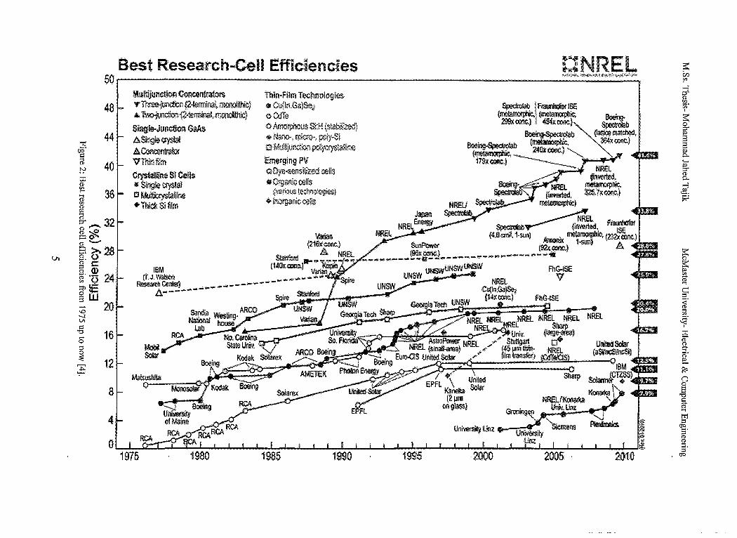
Figure 2 shows the history ofPV's evolution since the beginning of the industrial production. In
this picture, major improvements in the efficiencies of each type of SCs (Crystalline, Multiple
junction, Thin film, single junction and Organic photovoltaic) are shown by mentioning the time
3

Chapter 1: Introduction
and the name of the research group. As shown in the picture, the highest efficiency is for three
junction solar cells (from Boeing-Spectrolab R&D) with 41.6%.
For organic photovoltaic, it was in early years of 60's that researchers noticed the potential of
organic materials in imaging systems [11]. During the next couple of years, investigation in the
field of organic photovoltaic (or OPV) continued but efficiencies were really low. As' an
example, 0.001% efficiency reported by C. W. Tang et.al. in 1975 was the state of the art. In
1977 Heeger, MacDiarmind and Shirakawa discovered that by introducing doping such as
halogen chlorine, bomine or iodine, the conductivity of the conjugated polymer can be increased
by the range of eleven order of magnitude [12]. Later on, in 2000, they received a Nobel Prize in
Chemistry because of their great works on conductivity and superconductivity in organic
materials [13]. The first OSC with efficiency over 1 % was reported in 1986 once again by C. W.
Tang [14].
The latest development is related to Solarmer Energy Inc. On 27 July 2010, Forbes.com reported
that Solarmer broke the 8% wall and reported an organic solar cell with 8.13% efficiency [15].
As Forbes reported, the president of the Solarmer Company refelTed to the 8% efficiency wall as
the "psychological balTier for the OPV industry". Forbes predicted that by this discovery, the
cost of energy production for OPVs will go down to 12-15 cents/kWh.
4
VI
Best Research-Cell' Efficienc,ies ~:lN'R E IL 50 ,j ?'i.it~~r.;)~., !~~'to~:iX.~.s,?ri::j>~.~ l...<l:,~::<¢:'-:"~~~'U
>;:j
qq' ~ .... CP tv
to ~ ..... ~ en CP
48
44
40
36
8 ; _32 ~~ CP-
S >. ·28 C'l 0·· ~r c: 8. Q) ~ '0 24 ~E SW ~ 20 -..J Vl
.§ ..... o
~ ~
16
12
8
4,
0
I
I
Thin·Fillm Technoio<gies .. Cu{ln;Ga)Se;l
M!JltrJu~dC)n C«l~mrat{)f'S "Th~n (2-!ermlnal, 1OOfd1lhfr;) A i~!1r;llon '(2·termin?I,~ic)
Siogf$.Junctioo GaAs ~$inglt;t~1
IJ!J.~ VThinfilm
oCdTe 0. ArIlorphous Si:.Hl (stabi!12.00) ,.. Nano-, micro-, po!)'~Si
(~ I frnunl;(!fer lSE 299x ~IC'! (me~_1e,
(IC('Ic.)! 454.x.conc;) ~ . BoeiI1lt'Spedr<ll'ab~. ~b
Crystamne Sf Cells III, Single crys.Ia'l Il MulOCtysl;aUine +ihil;:kSifirm
1:1' 'M~j!tii\lllv"Wn PC:lI1cry'S(allll'le
Em~rglngPV 0' Dye"'5ensluzed ceUs iii! Omanil::oolfs
\\I(l!!QUS tltCl1noiogi€s} *lrlOrganic ~l!s
S¢E1ng-Spe.:;\~b (metiwoorpbIC . {~malched, (me!a~, .240~(#I },364>;.IlQIlC,.) fi'9xoooc.1 - __ -.. c. "'.... "-_~~, .. ... 9"
:;:~/J~;~-.. .. ~lIwerted,
rootamo.~
Varian ~ .. 121"''' • ""'" <_ .....
A
'" ~-,,, . ,
". . "'""" . NREt ""'_ (4.0"", ,...., """"'.-.
,.1;;"..... I"",,,,oj"-;.;~-I-' ---.--- ".""",,1 -~. • ... """'1 . ..... '" ---a -~. ------ ''','''''' I .-1 "' ___ ---~-------------------- ,. .,.. _ . _________ --.. _. A Spite UNSW UNSWUNS'!IJ UNlSlN
"'" ....... UNSW ~ .. . FhG ....
Sar6a. ARCO .- V ..... w....,. UNSW"""" . ~J$o, RCA !.lib house ~.. n .... GexgiaTt:¢li $bp. GecG"giaTed1 UNSW (14,;,cooe.) FIt4j·tSE No, . ~ ~~:::;§~.;=:~JI~=t~-or-........ ---a 'Sta=a... .. !J~i¥erniLy ~.~~ ~/""NRkL .NrlL. . . NteL N~L" • . . V = ...... ',,;:»--"" . ." ORE . L . ..... NREl
Kodlik......, ARCO"'" . . N .-. oni"~ _ ,../';- . "'" .--" . REt I_I NREl /'...... .-~-i • _ ~.:.I .. Boei. "ng EUro-Of.S ~.unitOO$Q ... l8t . <iii'''' 1
45, .(:Iil1WIi-. ~ n_. ""'" _ . . . - ".""sfoj """" ~..,.. "'~~I , 0 o . .....;.::.; ........... ~
t~ Solar
Matsus/lila (
1975 1 'gaS 1990 2005 ' 2010
~ CI.l en
~ ~. en I
~ ~ '" p..
~ p..
>-l 2:: . ~
i '" en
~ §r ~. en
f' ~ CP
8-o· e:.. go () o .§ ~ ....
H ~. CP
s· Oti

Chapter 1: Introduction
1.2. ORGANIC SOLAR CELLS
1.2.1. WHY ORGANIC SOtAR CEU:r
Compared to conventional solar cells, organic solar cells are relatively cheaper to produce. The
obvious reason is that the type of materials used in organic solar cells are less expensive, needs
less preparation and is more abundant than conventional crystalline solar cells.
Organic materials are polymers and oligomers as well as organic molecules very similar to the
plastic bags that we use every day. Similar to plastic bag, they are products of oil. Therefore, in
the case of mass production, their price can be really low.
On the other hand, unlike conventional solar cells that are based on crystalline semiconductors,
which need high purity in material and therefore, costly preparation and purification processes,
organic materials that are used in organic solar cells are easy to process with very cost effective
processes.
Because of malleability of organic materials, organic solar cells are capable of getting into ~ny
shape during the process of fabrication and the final production can also be a flexible sheet that
can be wrapped and packed for example into a soldier's backpack and in the case of necessity for
recharging an electrical equipment be unwrapped and used.
Moreover, the fabrication methods for organic solar cells are much cheaper than conventional
solar cells. As an example they do not need a clean room facility for their fabrication procedure.
The deposition processes in the case of molecular and polymeric thin film are spin-coating,
screen printing, spray coating and ink jet coating, reel to reel printing [5], which are low cost,
simple and they are also suitable for large area and ultra thin layer fabrication, which in the case
of mass production make the whole process of fabrication extremely cost effective.
6

M.Ss. Thesis- Mohammad Jahed Tajik McMaster University- Electrical & Computer Engineering
Figure 3: A reel to reel printing machine in CSIRO institution, Australia [6]
Figure 3 shows a reel to reel printing machine in Commonwealth Scientific and Industrial
Research Organisation (CSIRO). This machine uses the same technique that is used in printing
news papers. The machine in Figure 3 is capable of printing 200 meters of organic solar cells per
minute in the full speed condition. This is equal to printing 100km of solar cells per day.
Assuming that the efficiency of the printed solar cell is close to 10%, continuous printing at full
speed for five months will provide enough solar cells to generate 1 G watt electrical power plant.
All of the mentioned reasons above plus this fact that their efficiency is still really IQw,
compared to the conventional solar cells, make the organic solar cell a prospective and
interesting research topic.
1.2,2, DIFFERENCES BETWEEN ORGANIC AND INORGANIC SOLAR CELLS
The first difference between organic and inorganic SCs is due to the materials that are used to
make them. As it can be deduced from the names, in the inorganic SCs, inorganic materials such
as crystalline materials (mostly silicon-based) are used. These SCs have good electrical
properties, which are mostly because of their crystalline structure. On the other hand, they have a
relatively low light absorption, which can be corrected using a multistage structure.
7
Chapter 1: Introduction
Once again as the name implies, organic SCs are made of organic materials. Organic SCs based
on their materials can be divided to the following categories:
1- Dye-sensitized OSCs
2- Molecular SCs
3- Polymeric SCs
4- Mixed SCs
Organic dye-sensitized SCs (ODSSC) are made of a liquid electrolyte that transports generated
carriers created by organic molecules inside the electrolyte. This type of OSC is very cheap but
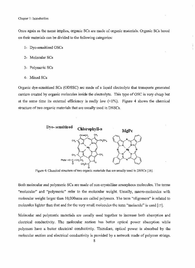
at the same time its external efficiency is really low «1%). Figure 4 shows the chemical
structure of two organic materials that are usually used in DSSCs.
Dye- sensitiz ed Chlorophyll"'a
Both molecular and polymeric SCs are made of non-crystalline amorphous molecules. The terms
"molecular" and "polymeric" refer to the molecular weight. Usually, macro-molecules with
molecular weight larger than 10,OOOamu are called polymers. The term "oligomers" is related to
molecules lighter than that and for the very small molecules the term "molecule" is used [17].
Molecular and polymeric materials are usually used together to increase both absorption and
electrical conductivity. The molecular section has better optical power absorption while
polymers have a better electrical conductivity. Therefore, optical power is absorbed by the
molecular section and electrical conductivity is provided by a network made of polymer striIigs. 8

M.Ss. Thesis- Mohammad Iahed Tajik McMaster University- Electrical & Computer Engineering
Figure 5 and Figure 6 respectively show the chemical structures of some molecular and
polymeric materials that are used in fabrication of OSCs with their abbreviated names.
PTCRI
l\ll'-PTCDI o~.o -N tI
"l 'I o - - 0
Molecular SCs PTCDA
o~. '10
ci ~ 'I 0
o - -- 0
,r{}--(h ..rO o-rN'--O--Q-tN A
o 1>IPc (1I..B1Zn. CU)D_
1I1Pf JJ-. D-cQH N Hbo ~N-f-N~
TPyP
"M" N'Er C60
TPD
Another major difference between conventional and organic SCs is due to the mechanism of
charge generation and charge transport. In inorganic SCs, after the absorption of a photon, an
electron is excited and an electron-hole pair is generated. Then, because of the build-in electrical
field, which is due to the difference in anode and cathode work functions, inside the device they
are separated from each other. After separation, because of electrostatic charges that each one of
them has, they would be drifted towards anode (for electrons) and cathode (for holes). Figure 7
shows a schematic depiction of a conventional SC that mimics the mechanism of charge
generation inside a conventional SC. In the case of organic SCs, electron and holes are tightly
bound together and make an exciton (Figure 7).
9

Chapter 1: Introduction
lVl[)l\fO-PPY
PTPTB C H
~1~22n~_ s ~r~}Q .. NI
N~
Polymeric SCs Figure 6: Chemical structures of some of the famous polymers that are used in OSCs [16]
The binding energy of organics' excitons and their separation energy is a little different than
conventional semiconductor excitons. In both of them coulomb attraction between the electron
and hole exist and to break the exciton that barrier of energy should be overcome. However, in
the case of organic excitons, the situation is a little different. An exciton in an organic segment (a
molecule or a string of a polymer) is equal to the excited state of that segment. It is one of the
stable states in the discontinuous energy states of that segment and is related to a stable orbital
form of electron cloud of that segment. Therefore, breaking an organic exciton is equivalent to a
change in a stable state, which requires an amount of energy that is more than the coulomb
attraction.
10

M.Ss. Thesis- Mohammad Jahed Tajik
Conventional Solar Cell
c: electrons
)
)
holes
McMaster University- Electrical & Computer Engineering
Organic Heterolunctlon Solar Cell
holes
)
electrons
Figure 7: Schematic of a inorganic SC (left) and an organic heterojunction SC (right) [18]
On the other hand, unlike conventional semiconductors, there are no crystalline structures in
organic materials for the separated charges. Single charges in an organic material are bound to a
site and are called a polarons. Consequently, before the separation of charges, there should be a
second molecule to carry one of the separated charges. This means that there is more energy that
is required to break an exciton and therefore, one more phenomena other than the coulomb
attraction to bind opposite charges inside an organic segment to make an exciton.
Since an exciton has both types of charges, it cannot be attracted towards any of the electrodes
due to the internal build-in electrical field. However, like many other particles, they can diffuse.
If an exciton gets to a conductive layer, electron and hole will be recombined at the surface of
that conductive layer and as a result, no electrical power will be generated. Consequently,
electrons and holes should be separated before that. To generate an electron-hole pair out of an
exciton, one of the following conditions should exist:
1- High electrical fields
2- Interface of two materials with two different energy bands
11
Chapter 1: Introduction
Because of the low build-in potential in organic solar cells, using heterojunctions, the second
condition is used in the structure of the OSCs to break up the excitons. In the next section,
different structures of OSCs are discussed.
1.2.3. DIFFERENT TYPES OF ORGANIC SOLAR CELL
Similar to conventional solar cells, there is a type of organic solar cell with an active layer made
of one of the n-type or p-type materials (mostly p-type). The name of this kind of organic solar
cell is Schottky OSC because of a Schottky connection in one side of the device. Figure 8 shows
a schematic structure and band diagram of a Schottky-type SC.
Organic
Anode
LUMO
Schottky contact
Ohmic contact
Figure 8: Schematic ofa Schottky-type organic solar cell with its energy band diagram [16]
Since there is no interface in the design of this device, most of the generated excitons are going
to be dissociated at the interfaces or inside the active layer without generating any power.
Therefore, the next structure is proposed with two types of organic material as its active layer.
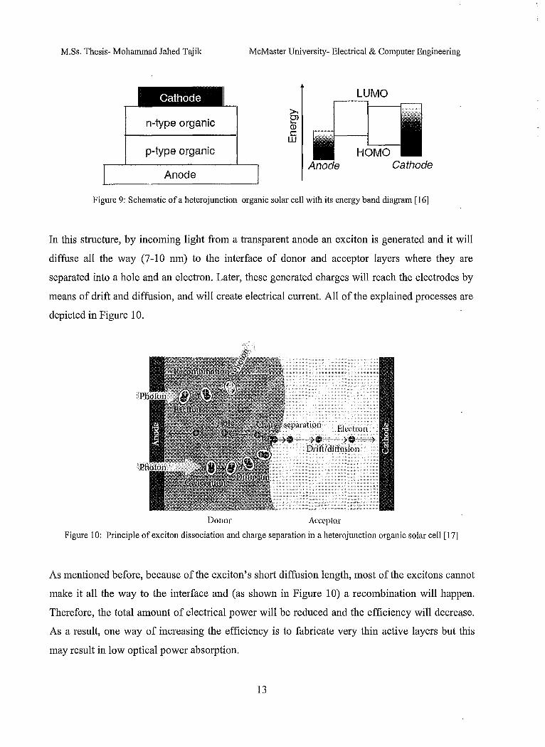
This structure, due to the use of different layers, is named heterojunction organic solar cell (or
bilayer heterojunction OSC). Figure 9 shows the schematic and band diagram of a
heterojunction SC.
12
M.Ss. Thesis- Mohammad Jahed Tajik
n-type organic
p-type organic
Anode
McMaster University- Electrical & Computer Engineering
LUMO
HOMO Cathode
Figure 9: Schematic of a heterojunction organic solar cell with its energy band diagram [16]
In this structure, by incoming light from a transparent anode an exciton is generated and it will
diffuse all the way (7-10 urn) to the interface of donor and acceptor layers where they are
separated into a hole and an electron. Later, these generated charges will reach the electrodes by
means of drift and diffusion, and will create electrical current. All of the explained processes are
depicted in Figure 10.
Electron -7e-·---:·H!)~
Drift/dilInskH1
Donor Acceptor
Figure 10: Principle of exciton dissociation and charge separation in a heterojunction organic solar cell [17]
As mentioned before, because of the exciton's short diffusion length, most of the excitons cannot
make it all the way to the interface and (as shown in Figure 10) a recombination will happen.
Therefore, the total amount of electrical power will be reduced and the efficiency will decre~se.
As a result, one way of increasing the efficiency is to fabricate very thin active layers but this
may result in low optical power absorption.
13
Chapter 1: Introduction
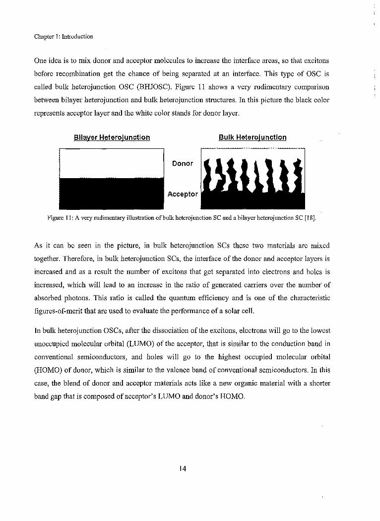
One idea is to mix donor and acceptor molecules to increase the interface areas, so that excitons
before recombination get the chance of being separated at an interface. This type of OSC is
called bulk: heterojunction OSC (BHJOSC). Figure 11 shows a very rudimentary comparison
between bilayer heterojunction and bulk heterojunction structures. In this picture the black color
represents acceptor layer and the white color stands for donor layer.
Bilayer Heterolunction Bulk Heterojunction
Donor
Acceptor
Figure 11: A very rudimentary illustration of bulk heterojunction SC and a bilayer heterojunction SC [18].
As it can be seen in the picture, in bulk heterojunction SCs these two materials are mixed
together. Therefore, in bulk heterojunction SCs, the interface of the donor and acceptor layers is
increased and as a result the number of excitons that get separated into electrons and holes is
increased, which will lead to an increase in the ratio of generated carriers over the numbet of
absorbed photons. This ratio is called the quantum efficiency and is one of the characteristic
figures-of-merit that are used to evaluate the performance of a solar cell.
In bulk: heterojunction OSCs, after the dissociation of the excitons, electrons will go to the lowest
unoccupied molecular orbital (LUMO) of the acceptor, that is similar to the conduction band in
conventional semiconductors, and holes will go to the highest occupied molecular orbital
(HOMO) of donor, which is similar to the valence band of conventional semiconductors. In this
case, the blend of donor and acceptor materials acts like a new organic material with a shorter
band gap that is composed of acceptor's LUMO and donor's HOMO.
14

M.Ss. Thesis- Mohammad lahed Tajik McMaster University- Electrical & Computer Engineering
D\.
Au
Bulk heterojunction I
Figure 12: Schematic of the band structure in bulk heterojunction solar cell [19].
In this thesis, both the bilayer heterojunction and the bulk heterojunction are modeled. The next section
describes the organization of the thesis, order of subjects and the reasoning behind them.
1.3. ORGANIZATION OF THE THESIS
The goal of modeling organic solar cells is to find new device designs, to enhance the
understanding of the power generation in these devices and to improve the performance of these
devices based on the understanding. Modeling provides an opportunity to examine properties
that are out of reach or too expensive to measure. On the other hand, modeling is much faster and
makes it possible to study numerous device structures and configurations. in a very short period
of time, which can provide valuable information. These abilities are beyond what an experiment
can do. By taking the device as a light-in current-out device the performance of solar cells can be
divided into the following processes:
1- In-coupling of the photons
2- Absorption of the photons
3- Formation of the excitons
4- Diffusion of the excitons
5- Dissociation of the excitons
6- Transportation of the charges
15

Chapter 1: Introduction
7- Collection of the charges at the electrodes
In this research, all of the seven processes are studied. The rest of the thesis is organized as
follows.
The thesis body is divided into two chapters:
Optical model (chapter 2)
Electrical model (chapter 3)
Each one of the mentioned chapters has two sections:
Analytical analysis
Numerical analysis
Each section consists of one or two models. Regardless of the type of the models, each model
has two sections:
Description of the model
Results and discussion
The thesis starts with optical chapter (chapter 2). The analytical analysis of the optical properties
of the organic solar cell is the first section of this chapter, which contains one model, Transfer
Matrix (TM) model. The reason for studying TM model is to create a reliable mean to test the
validity of the generated numerical models.
The next section is numerical analyses of the optical propelties. This section's ultimate goal is to
study the effect of focusing aperture at the top layer of an organic solar cell on the performance
of the device. This section consists of two numerical models:
Two dimensional optical model
Three dimensional optical model
The two dimensional model uses the "Harmonic Propagation" package whereas the three
dimensional model uses "PDE, coefficient form, Stationary analysis" package. The main reason
16

M.Ss. Thesis- Mohammad Jahed Tajik McMaster University- Electrical & Computer Engineering
for choosing the second package to model the three dimensional optical problem is the low
computational cost of this package compared to the Harmonic propagation package.
In the result and discussion part of the two dimensional model, after examining the validity of
the model by comparison with TM results, the effect of 18 different two dimensional light
focusing apertures or one dimensional photonic crystals is studied. The same pattern is repeated
for the three dimensional model with one difference that, this time the result of 14 different three
dimensional light focusing apertures (two dimensional photonic crystals) is studied. This
concludes, chapter two.
The next chapter (chapter 3) is related to the electrical modeling of organic solar cells. The first
section is related to analytical analysis of electrical modeling of bilayer heterojunction organic
solar cells. The model is based on the diffusion of excitons. The result is presented in the form of
"incident monochromatic photon to current collection efficiency" or shortly IPCE. Later, the
calculated IPCE is compared to the measurements and a good agreement is observed.
The second section of chapter 3 is about numerical modeling of electrical properties of a bulk
heterojunction solar cell. A self consistent loop of Poisson's equation and two separate continuity
equations for electrons and holes, and the multiphysical COMSOL model to solve them is
described. The results of this section are followed by a comparison of the obtained numerical
results with numerical results reported in the literature. Later, numerical results and measurement
results are also compared and some dissimilarities are observed.
To address the observed dissimilarity issue, a theory based on tunneling current at the interface
of metallic electrode is developed. Based on that, the best fit to the I-V curve of experimental
and numerical results is found using trial and error and the optimal values of the parameters of
the tunneling current are determined. Finally, the last chapter (chapter 4) is the conclusion and
suggestions for future works.
17

M.Ss. Thesis- Mohammad lahed Tajik McMaster University- Electrical & Computer Engineering
CHAPTER 2
OPTICAL MODELING
2. OPTICAL MODELING
This chapter is dedicated to optical modeling of organic solar cell. The goal is to find the
magnitude of electrical field inside a planar organic solar cell as a function of position and
incoming light's frequency. Using the calculated electrical field's magnitude, the intensity of
light is calculated as a fllnction of position and frequency of the incoming beam. Then, the
amount of absorbed power and based on that the total number of generated excitons is calculated.
Therefore, outputs of optical simulation are:
1- Profile of light intensity as a function of position and frequency
2- Amount of absorbed power as a function of position and frequency
3- Total number of generated excitons as a function of position
The following, models that have been used to calculate these results are described. This chapter
is divided to two sections:
1- Analytical model
2- Numerical model
For the analytical section, the transfer matrix method (or shortly TM) was used. The TM method
is a straight forward method that can calculate the distribution of electromagnetic waves in a one
dimensional structure. It can be successfully used for the optical simulation of multilayered thin
film solar cells. However, due to its analytical nature, it is difficult to develop a TM-based
18
Chapter 2: Optical Modeling
optical simulator for complicate geometries, for an instance folded structures or planar solar cells
with focusing structures.
For the numerical section, we used "COMSOL Multiphysics". This software benefits from Finite
Element Method's (or shortly FEM) excellent compatibility with unorthodox boundary
conditions. It is also equipped with advanced abilities in modeling capabilities such as adaptive
meshing and controllable damping parameters. Moreover, it is possible to link COMSOL
Multiphysics to other programming platforms such as MATLAB, in order to perform joint
simulations. These make COMSOL Multiphysics a proper choice.
Prior to finalizing the decisions on using COMSOL as the numerical modeling environment, a
few other packages were also examined. Among them were Finite-Difference Time-Domain
(FDTD) Solutions (by Lumerical Solutions, Inc.) and OptiFDTD (by OptiWave system Inc.),
that have a purchased license at McMaster University. Most of them use the FDTD method as
their modeling strategy which makes them a good candidate for a time dependent or transient
analyses, while we were interested in harmonic analyses.
On the other hand, incomplete libraries that lack organic material coefficients made it necessary
to create new libraries that needed precise information about the development of the software.
Obtaining this knowledge about each one of the softwares to decide which one is changeable was
simply time consuming and it questioned the whole Idea of using software in the first place.
Moreover, finite difference is not the best numerical method to model problems with peculiar
geometry. All of the mentioned advantages for COMSOL plus the ability of modeling the
electrical section of the simulation in COMSOL at the same time and linking two sections of the
simulation (electrical and optical), made the software COMSOL multiphysics the ultimate choice
for this research.
The optical numerical model is also divided into two separate sections:
1- Two dimensional model
2- Three dimensional model
19
M.Ss. Thesis- Mohammad Jahed Tajik McMaster University- Electrical & Computer Engineering
For the two dimensional section, the "Harmonic propagation" package was used. But because of
the high computational cost of Harmonic propagation package for the three dimensional model,
the three dimensional simulation was performed by using a less complicated package: "PDE
coefficient form, stationary analysis".
2,1. OPTICAL MODEL, ANALYTICAL ANALYSIS
2.1.1.. TRANSFER MATRIX METHOD ('I'M)
Transfer Matrix approach (TM) is one dimensional modeling of light propagation through the
different layers of a planar solar cell, which can be attributed as a one dimensional layered stack
of different materials (Figure13).
air
z
j incident light
~'R'~~~~rq z= IJ,
z'" D,
z= D,,=O
Figure 13 : A planar solar cell in the presence of ambient incident light [20]
2.1.1. t. Description of the 'I'M Model
In this method, the solar cell is modeled by using two types of matrices:
1- Layer's matrix, which models the effect of each layer's material on transporting beam of
light.
20

Chapter 2: Optical Modeling
2- Interface's matrices, which model the phenomena of transportation and reflection of
incoming beam oflight at the interface of two adjoining layers.
(il) ------r-~~--~---
prim system bis system
(a) j
(b)
> ;; --, bis system , .~ ·~E~fl
.....
M E~~If-'_i --E-; prim system
E';" EiJJ~
r------~ '----\
(oj E,==1~ Figure 14: Demonstration of the layer and interface matrices, the left side is the interface of two layers and the
picture on the right side shows the propagation of light inside a layer [16]
The picture a at the left side of Figure 14 shows the interface of two layers. In the picture below
that, which is marked by word b, the traveling beam of light from layer i into layer) is shown by
E/. At the interface of two layers, this beam is divided into two elements:
Transported ray, which is shown by E.i +.
Reflected ray, which is shown by Ei-.
The relationship between these elements and the incoming beam of light is defined by the
Fresnel complex transmission and reflection coefficients as:
Equation 1
Equation 2
21
M.Ss. Thesis- Mohammad Jahed Tajik McMaster University- Electrical & Computer Engineering
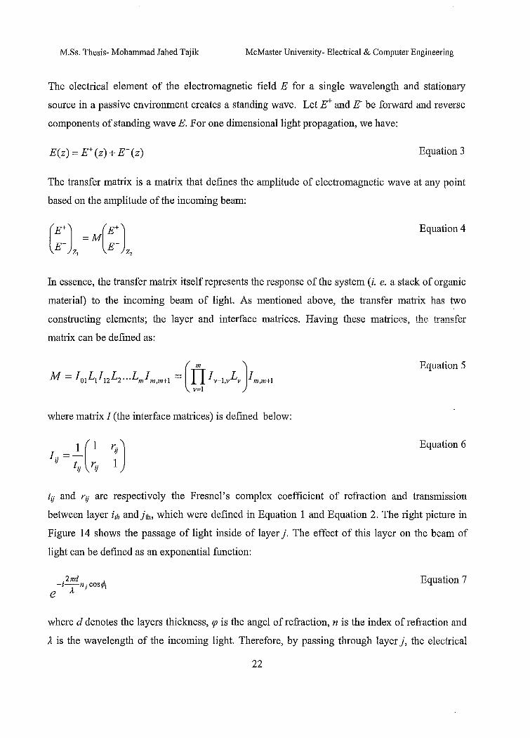
The electrical element of the electromagnetic field E for a single wavelength and stationary
source in a passive environment creates a standing wave. Let E+ and E be forward and reverse
components of standing wave E. For one dimensional light propagation, we have:
E(z) = E+ (z) + E- (z) Equation 3
The transfer matrix is a matrix that defines the amplitude of electromagnetic wave at any point
based on the amplitude of the incoming beam:
Equation 4
In essence, the transfer matrix itself represents the response of the system (i. e. a stack of organic
material) to the incoming beam of light. As mentioned above, the transfer matrix has two
constructing elements; the layer and interface matrices. Having these matrices, the transfer
matrix can be defined as:
Equation 5
where matrix I (the interface matrices) is defined below:
Equation 6
tij and rij are respectively the Fresnel's complex coefficient of refraction and transmission
between layer i1h andjth' which were defined in Equation 1 and Equation 2. The right picture in
Figure 14 shows the passage of light inside oflayer j. The effect of this layer on the beam of
light can be defined as an exponential function:
e .27fd d. -1-n.cosl"l A. J
Equation 7
where d denotes the layers thickness, q; is the angel of refraction, n is the index of refraction and
A is the wavelength of the incoming light. Therefore, by passing through layer j, the electrical
22
Chapter 2: Optical Modeling
component of the electromagnetic field has a phase change equal to the argument of the
exponential function in Equation 7 which depends on the refractive index, wavelength and width
oflayerj. Having all of the variables, layer's matrix is described as:
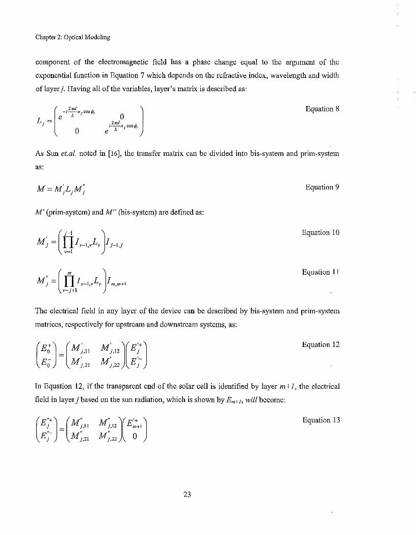
L -j -[
.21fd ¢ -z-njcos I
e A
o
Equation 8
As Sun et.al. noted in [16], the transfer matrix can be divided into bis-system and prim-system
as:
Equation 9
M' (prim-system) and M" (bis-system) are defined as:
Equation 10
Equation 11
The electrical field in any layer of the device can be described by bis-system and prim-system
matrices, respectively for upstream and downstream systems, as:
Equation 12
In Equation 12, if the transparent end of the solar cell is identified by layer m+ 1, the electrical
field in layer} based on the sun radiation, which is shown by Em+], will become:
Equation 13
23

M.Ss. Thesis- Mohammad Jahed Tajik McMaster University- Electrical & Computer Engineering
0.02
0.017
0.016
0.014
0.012
0.01
0.008
0.006
1.9
1.$5
1.8
1.75
1.7
1.65
1.6
ITO refractive index
300 350 400 450 500 550 600 650 700 750
Wavel~ngth [om)
1.3
2.25
2.2
2.1
2.05
2
1.95
300350 400 450 500 550 600 650 700 750 Wav~I~l1gth{llm)
PEOPT refractive index
300350400 450 500 550 GOO 650 700 750 Wavelength [tlmJ
0.3 I· 4fc'i;
0.25
0.2
0.15
0.1
0.05
o
300 350 400 450 500 550 GOO 650 700 150 Wavelength [nm]
Figure 16: Refractive indices as a function of wavelength. For the following material with their references Al refractive indices [34], PEOPT refractive indices [35], PtEOP refractive indices [36], C60 refractive indices [37],
ITO refractive indices [38]
26
Chapter 2: Optical Modeling
PEOPT
1.2· lTO CSO, PECOT I AI
08 A)
OJ}
, \ " I
i \\c I t I I
\j I'--'! ! I i
OA
0.2
: .!
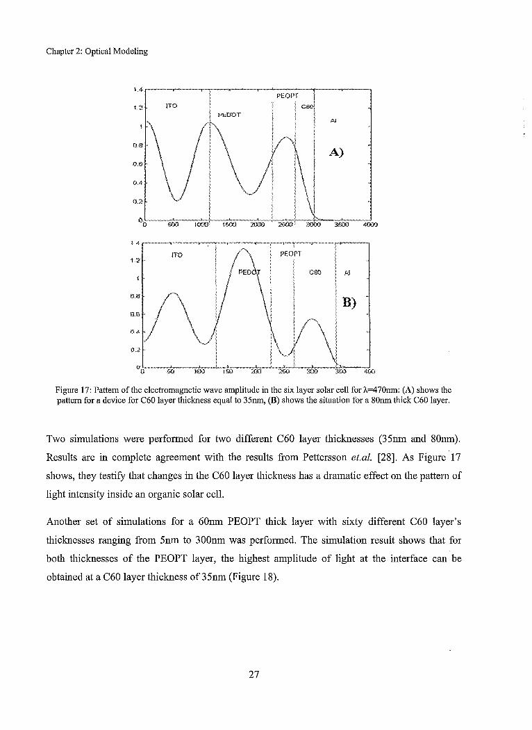
UO~--~,~~--~lrnID~i----l~~--~~~G~~~~'~-
Figure 17: Pattern of the electromagnetic wave amplitude in the six layer solar cell for A=470nm: (A) shows the pattern for a device for C60 layer thickness equal to 35nm, (B) shows the situation for a 80nm thick C60 layer.
Two simulations were performed for two different C60 layer thicknesses (35nm and 80nm).
Results are in complete agreement with the results from Pettersson et.al. [28]. As Figure 17
shows, they testify that changes in the C60 layer thickness has a dramatic effect on the pattern of
light intensity inside an organic solar cell.
Another set of simulations for a 60nm PEOPT thick layer with sixty different C60 layer's
thicknesses ranging from 5nm to 300nm was performed. The simulation result shows that for
both thicknesses of the PEOPT layer, the highest amplitude of light at the interface can be
obtained at a C60 layer thickness of 35nm (Figure 18).
27

M.Ss. Thesis- Mohammad Jahed Tajik McMaster University- Electrical & Computer Engineering
The parameters, which have been used so far, are as below:
Absorption coefficient, refractive indiceses (optical coefficients)
Thicknesses of the layers and their orders
Amplitude, angel and frequency of the incident beam
1.0~--------------------------------------------~ Our model I\) (,j
~ 0.8-I\) M ..... = .- -~ 0.6-U . - ~ ~ -o 0.4-~ ~ ~ . il-! _
.~ 0.2-<', ~
!5L
Patterson et.(ll.
0.0 -+'~~~-'~I~.~.~~.r-'Y-l~''-'~'-''~I~.r-r-r-~'~J~.-,.~.~,F-r-Ir-r-T-~ o 50 100 150 200 250 300
Thickness of C60 hlYer Figure 18: Amplitude of the electromagnetic wave at the active area interface for a 60nrn thick PEPOT layer and 60
different thicknesses of C60 layer, ranging from 5nm to 300nrn. The result is compared the literature [28].
All of the simulations up to this point were established for a single wavelength of incident light
(A,=470nrn), but the sun light has a vast spectrum. To better understand the behavior of the
device, the simulation was repeated for a range of wavelength from 300 to 800nrn, where the
incident light has an acceptable intensity. The optical modeling was also performed for another
device with different materials (ITO 120 nm, PedotPSS 110 nm, PFDTBT 40nm, C60 49nm, Al
30nm).
28

Chapter 2: Optical Modeling
2.2 ,...----,---,---,---,---,---,---,-----, 0.60
-1.4 200 400
o
-·-nll 0.50 ~ \
-~·/L
--·k~ ----·kz
< ___ -4 0.00
600
vVavelength (nm)
800'1000
ITO PedotPSS polymer eM AI
z 120 230 270
Figure 19: The second device configuration (shown below) and the refractive index of the polymer [poly(2,7-(9-(2'ethylhexyl)-9-hexylfluorene)- alt-5,5-(4' ,T-di-2thienyl-2',1' ,3'-benzothiadiazole))] [31]
This part of the simulation seeks the best design of a device with the most amount of light
absorption close to the active layer interface. Therefore, a set of 400 different solar cell
configurations consisting of different combinations of C60 and PFDTBT layers thicknesses
(ranging from 5nm to 100nm for each layer) with 17 different frequencies (from 300nm to
700nm) were tried. It is equivalent to conducting the simulation that had been performed to
obtain Figure 17, being repeatedly for 6800 different runs. Then, a double integration (an
integration over wavelength and another over position) over the absorbed power formula was
executed. The formula for the total absorbed power is as:
29

M.Ss. Thesis- Mohammad Jahed Tajik McMaster University- Electrical & Computer Engineering
Total absorbed power = J JQ(z,m) Equation 15
Jz
Q (z, w) is the average flow of optical energy dissipation at the point z (z axis begins from the
ITO-glass's interface and continues through the device) at the wavelength "w", The domain of
integration is from 1 Onm inside PFDTBT layer to 10nm inside C60 layer at the both sides of the
active layer's interface for position and from 300nm to 700nm for wavelength. Figure 20 shows
the result of the simulation, which is in a good agreement with the results reported in literature
[31].
90
80
70
60
50
40
30
20
10
o '100
. ~ .......... ~ , ~. • ' • ~ , s ' ' " ~ ~ •
~:, ~ . ~ . ~ . ":1"" , .. ' . :. .. ~
30 40 50 20 0 10 20 Polymer Thickess [nm]
":', · " "" .
", : . ~ ", · "
.... :. " .
: .... .... :.
· " ,-.
60
" . ,', . "
:"', ... ~
-,:.. , "
" ' "
", . "
70
. ~ i _
.',
T ... ,
,',
80
Figure 20: Light absorption as a function of polymer thickness and C60 thickness. The thickness ofPedot:PSS is 100nm and ofITO 120 nm
The Poynting theorem was used to calculate the absorbed power formula used in Equation 15.
Based on the Poynting theorem, "the amount of power dissipation at any point in a conservative
environment is equal to the divergence of the Poynting vector at that point multiplied by -1 H: '
Q(z) =-'1.S Equation 16
S denotes the Poynting vector. For an electromagnetic wave, it is equal to:
30

Chapter 2: Optical Modeling
1 S=-ExB
J1
Equation 17
The electrical field E is calculated by using Equation 14. For an electromagnetic field, we have:
E Equation-18 -=c B
where B is the magnetic field and c is the speed of light. Using Equation 16, Equation 17 and
Equation 18 , Q(z) can be written as:
Equation 19
As Figure 20 shows the best design is achieved for a polymer thickness of 10nm and a C60 layer
thickness of 50nm, which confirms the reported results in reference [31]. However, a change in
the thicknesses affects not only the light absorption of the device but also its electrical properties
such as internal resistances and as a result the I-V curve and therefore, the efficiency of the solar
cell. Another way to change the pattern of light intensity inside a solar cell is to have a focusing
mechanism at the top layer. In order to model such structures, analytical models such as TM are
not helpful and therefore, numerical methods are needed to be used. The next two sections are
dedicated to optical modeling of such structures using COMSOL multiphysics.
2.2. OPTleAL MODEL, NUMERICAL ANALYSIS
In this section, first basics of modeling a two dimensional Helmholtz's equation of light
propagation in a planar structure using COMSOL multiphysics is described. Then, similar to the
previous section, it is explained how the propagation of light can be modeled by calculating the
magnitude of the electrical component of the light wave (assuming transversal electric (TE)
polarization) inside a planar solar cell.
Finally, building on the framework developed in the previous section, Equation 15 is used to
calculate the amount of optical power that is absorbed close to the interface of the active layers.
Then, the power is compared for different light focusing deformities at the top layer.
31

M.Ss. Thesis- Mohammad Jahed Tajik McMaster University- Electrical & Computer Engineering
In the developed modeling framework, the magnitude of the electrical field is computed and used
to calculate the amount of absorbed optical power and then the number of optically induced
excitons.
As mentioned before, we take a beam of light as an electromagnetic wave that travels through
different environments. Equation 20 shows the plane wave formula that is being used to
characterize the electrical field:
E ( x, t) = Aei(k.x-mt) Equation 20
2.2.1. Two DIMENSIOi-JAt OPTICAL MODEt
2.2.1 J. l)escripHtm of the Two I)imensionalMo{ieI
This section presents the COMSOL-based model that was developed to capture the physical
essence of the optical phenomena under study. Also, extensive simulations were conducted to
validate the theory. It was tried to address the basic issues involved in building a COMSOL
model [33].
For building models in COMSOL, we benefited from the "Harmonic Propagation" modeling
package, from the TE branch of the "In-plane wave" folder of the "RF" module. Figure 21 shows
how this package can be found in the opening window of the COMSOL Multiphysics software.
!Ih~:i"1EMS ~" ~<j;RF Module ! 's<i In-Plane Waves i 1 8" •. 1£ Wa:;.ov,;::es ..... ____ _
! I t::~~ag::? ; \'"'. Transient propagation ~ i . l'~'". Scattered harmonic propagation Gr·. TM Waves rll' •. Hybrid·~1ode Waves
Figure 21: Accessing the Harmonic propagation package at the opening window of the COMSOL Multiphysics
In order to generate a model in this package, one needs to precisely define the boundary
conditions, sub domain expressions, type of the sources (planar, polar, etc.), material properties
32

Chapter 2: Optical Modeling
and the policy of the modeling (via writing scrip commands inside COMSOL or controlling the
whole COMSOL simulation from an external programming platform such as MATLAB).
After clicking on the "Harmonic propagation" in the opening window, which is shown in Figure
21, from the "Draw" option on the top toolbar one can draw the device geometries. At fIrst a
very basic planar device is modeled for two reasons:
The ease of explanation
To compare the results with the existing TM results
The next part of the modeling is defInition of proper meshing. By clicking on "free mesh
parameters" from the "Mesh" section of the top toolbar, maximum mesh dimension for solar
cell's sub domains and the environment that solar cell is in it are chosen to be 1O-7m and 4x lO-6m,
respectively. This arrangement of meshing parameters allows an accurate and yet effIcient
simulation set up. Boundary meshing parameters can be used to improve the accuracy of the
model by providing more information on the active junction (the interface of n-type and p-type
materials) .
Figure 22 is produced by using the mentioned values for the parameters for the sub domains and
setting the maximum of mesh distances on the active interface equal to 1 x 10⁻⁸ [m]. After
importing all of the parameters for meshing, COMSOL creates the mesh for the planar solar cell
as depicted in Figure 22 using an adoptive algorithm for triangular meshing,.
Figure 22: Meshing of a planar solar cell via adaptive meshing.
33

M.Ss. Thesis- Mohammad Jahed Tajik McMaster University- Electrical & Computer Engineering
The next section explains the boundary conditions and we begin with the optical source as the
first boundary condition. Figure 23 shows the power spectrum of sunlight for AM 1.5 ("AM"
stands for air mass and 1.5 is the coefficient that characterizes the solar spectrum for an absolute
air mass of radiation at zenith angle of 48.19°s standardized by ASTM (American Society for
Testing and Materials). As is shown in Figure 23, the important part of the solar spectrum (300-
700 nm) is given to COMSOL by defining a function named sunlight. Later, it will be explained
how a MATLAB or script based model can be run for each given wavelength in Figure 23.
1.6
1.6
/
0.8 / mo 1Il00 1 mo 2aJO 28lO 3IlD ~S(l 400 4;i;l soo ssa §I)(l "'so 700 750
Waw-.th [rm1 x Figure 23: Spectrum of the sun (left) [32], Solar spectrum given to COMSOL (right).
Sunlight is modeled by a planar TE wave source which is described by a planar wave in
Equation 20. The organic solar cell that we are going to model can be considered as a lossy
object in the middle of a waveguide, which has an even excitation at one of its ports.
Consequently, the optical source is an excitation at one end of the environment with different
magnitudes for different wavelengths to model the sunlight's spectrum in Figure 23.
The boundary conditions can be selected as shown in Table 1. These boundmy conditions are
provided by the "Harmonic Propagation" package and there is no need to add any new
conditions. The next section answers the following question: "What is the equivalent physical
and mathematical contributes of these boundary conditions?" Also, the boundary conditions for a
three dimensional optical model will be described.
34

Chapter 2: Optical Modeling
a e oun ary con 1tions T bl 1 B d d" fi h H or t e k armomc propagatlOn pac age Energy port with rectangular mode, transverse electric
(TE), mode number of 10 and energy equal to Source of light sunlight's energy at that wavelength
Continuity
Interface of two materials with different refractive (this is the default boundary condition in any interface) indiceses
Boundary facing the source of light Energy port with rectangular mode, transverse electric (TE), mode number of 10 and zero energy at that
(the other port of waveguide) wavelength
To define the sub domain, the refractive index is chosen as shown in Figure 24. Later, the
refractive indices can be defined as a function of wavelength as shown in Figure 16. As Figure
16 shows refractive indices are composed of two parts: real and imaginary refractive indices (or
exciton coefficients):
n = 1J+iK
t~lllJdRmain Settings ~'in~PI~Q~''rE&v~~~;s'(ttwe) Equation
VX(VXEz) - n2Jc1/Er = 0, 0, = n2
, iJ, = 1, (J = 0
!subdomains i,GP?~p2.l_ I Subdomain selection
I I
Material properties , ..................................... , Library material: ",,,.gee,,,.',,,?,,,,,." •.. :.,, l!sl1::::!gj[~J
Quantity Value/EXpression Unit Description
(~Specify materlal properties ll) terms of rerractive index
n c.e ....................................................... _ ................................. -' 1 Reli'actfve Index
(j SpeCify material prc-perties in terms of or' pr,and a I L···· .. ·_ .. ·iccc::c::::::::c,,,::o:o::::c::::::o::oc:!
I Group: : ................................................... : 6, Relative permittivity
i 0 Select by grQup a : Sim Electric condu.:tivity
Equation.21
I ~i ~~~i::I~~~domanJ : ...................... _p._' ............. _ .......................... _ .......................................... _ .. _._._._ ...................... 1 .............. _R ... € .... I .. a .... t ... i.v ... e ...... P .... 8 .... r .... n .... _.e .. a .... b .... iI ... i_ty .... _ ........ :
Figure 24: Subdomain settings for the Harmonic propagation package
In this figure, refractive indices of five different materials (AI, PtEOP, PEOPT, ITO and C60)
are presented and the refractive index of the environment was assumed to be equal to the
refractive index of air (n=l).
35

M.Ss. Thesis- Mohammad Iahed Tajik McMaster University- Electrical & Computer Engineering
2.2.1.2. Two Dimensional Model, Rt'tmlts }lud Discussion By applying the mentioned coefficients and boundary conditions, the result for the planar solar
cell can be obtained. To make sure that the COMSOL model is reliable, the same device was
modeled once again, using the TM method and the results were compared to make sure that they
are compatible [28]. As shown in Figure 25, the results of two dimensional models and the TM
method are in good agreement.
As mentioned before, studying the effect of the focusing aperture was the main reason for
developing a numerical method to model the propagation of light inside an organic solar cell.
These focusing apertures are also called "capping layers" [29] or "light trapping aperture" [30].
They can also be attributed as one dimensional photonic crystals. Figure 26 shows the result of
samples of focusing structures. In Figure 26 the magnitude of electrical field is shown by the
coior of the pictures. In piaces with higher magnitude of electrical field, which is directly related
to the intensity of light, the color of the picture is red and in places with lower magnitude of
light, the color is blue.
Up to this point, the magnitude of the electrical component of the light electromagnetic wave for
a two dimensional structure is calculated. Similar to the previous section (TM modeling), the
next step is to find which structure wi11lead to a better efficiency. Therefore, the amount of
optical absorbed power close to the active layer interface for different light focusing structures
should be calculated and compared.
36

Chapter 2: Optical Modeling
Transfer Matrix Method Result ELECTRIC AL FIELD'S MAGNITUDE INSIDE OF THE SOLAR CElL
o 50 100 150 200 l50 300 -}SO 400
DEPT OFTHE DEVICE [nmj
0.8
0.6
0.2
----------------' Nin: 2.167e-3
Figure 25: Comparison ofTM and COM SOL results.
37

M.Ss. Thesis- Mohammad Jahed Tajik McMaster University- Electrical & Computer Engineering
Figure 26: Some capping structure and their effect on profile of light on the device.
To do so, all of the material refractive indices (Figure 16) were given to the software as a
function of wavelength. Then, parametric analysis of COMSOL was used with wavelength as the
changing parameter, ranging from 325nm to 700nm by 25nm steps. Finally, by using Equation
15 to Equation 19 and integration over frequency and position, total absorbed power ~as
calculated.
Figure 27: Three dimensional equivalent geometries ofthe modeled solar cells with three different forms oflight trapping structure at the first layer.
The schematic of the geometry of solar cell with three different types of light focusing apertures
(triangular, rectangular and semispherical) are shown in Figure 27. This figure shows the three
dimensional counterpart of our former two dimensional models.
38

Chapter 2: Optical Modeling
: : 50 •••• ? •• y," _.}" -, - • ~ ... , ,! ~. ¥.".
'E 40 ·····'·"yvnJTH( .. "·"· ·, .. '··· .. 'r'·"·"·'r .. · :;:,
20nm -'=~-40nm
80nm -'IOOnm _~d"'" 200nm -" -30011m --Flat
WIDTH ~ 30 i..
;t::
.... ""'~"'~~."!' .... ~.~ •••••••••• ~ ...... h ••••
of: « 20
10
goo 350 400 450 500 550 600 650 700 Wavelength [nmJ
Figure 28: The intensity oflight at the interface ofC60 and PEOPT for wavelength between 300nm to 700nm, using triangular arrays at the first layer,
Figure 28 shows the magnitude of the electrical field at the active layer interface as a function of
wavelength for the same solar cell structure that is shown in Figure 25 with an extra triangular
light focusing layer at the top. The triangular light focusing aperture is made of equilateral
triangles that are repeated without any distance. Different colors in Figure 28 represent different
base width of the triangular light focusing aperture (20nm, 40nm, 80nm, 100nm, 200nm and
300nm) while the height of the triangles are the same and is equal to 40nm. The refractive
indices are reported in Figure 16. The color black in this figure shows the amplitude of electrical
field in the absence of light focusing layer or a solar cell with a flat surface.
The same type of calculation that have been performed to produce Figure 28 is repeated for
Figure 29, with one difference that the light focusing layer used to create Figure 29 is made of
rectangular light focusing apertures. A rectangular light focusing layer consists of an array of
rectangular cubes repeated by a distance equal to their bases. An example of rectangular light
focusing layer can be seen in Figure 27 (the middle picture).
39
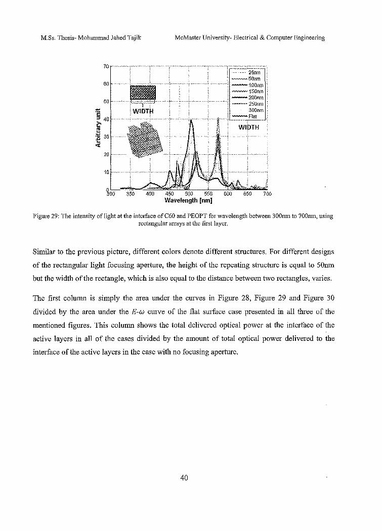
M.Ss. Thesis- Mohammad Iahed Tajik McMaster University- Electrical & Computer Engineering
20
Soo 350 400 450 500 550 Wavelength [nm)
650 700
Figure 29: The intensity of light at the interface of C60 and PEOPT for wavelength between 300nm to 700nm, using rectangular arrays at the first layer.
Similar to the previous picture, different colors denote different structures. For different designs
of the rectangular light focusing aperture, the height of thc repeating structure is equal to 50nm
but the width of the rectangle, which is also equal to the distance between two rectangles, varies.
The first column is simply the area under the curves in Figure 28, Figure 29 and Figure 30
divided by the area under the E-UJ curve of the flat surface case presented in all three of the
mentioned figures. This column shows the total delivered optical power at the interface of the
active layers in all of the cases divided by the amount of total optical power delivered to the
interface of the active layers in the case with no focusing aperture.
40

Chapter 2: Optical Modeling
200
180
'160 .,.."
60 " ..
40· ....
20
goo 350 400 13S0 700
Figure 30: The intensity of light at the interface of C60 and PEOPT for wavelength between 300nm to 700nm, using semicircular arrays at the first layer.
The calculation is the same for Figure 30 with this difference that the repeating structure is made
of an array of semicylinders with five different radiuses (25nm, 50nm, 75nm, 100nm and
125nm).
In order to find the best structure, four different parameters were calculated for all of the
eighteen light focusing apertures. All of them were normalized by the case that there was no light
focusing mechanism (i.e. by dividing the result to the result of flat surface simulation). All of the
results are shown in Table 2.
The second column is the result of integration of Equation 19 over the frequency and position
domains using PEOPT's absorption coefficient as a and calculating IEI2 using the magnitude of E that can be found in Figure 28, Figure 29 and Figure 30, divided by the result from the flat
surface case. Therefore, this column shows the ratio of absorbed power close to the active layer
interface divided by the result of flat surface organic solar cell.
41

M.Ss. Thesis- Mohammad Jahed Tajik McMaster University- Electrical & Computer Engineering
Table 2: Results of the simulation for the ~n"rhlrp~ normalized to the flat surface results.
Total optical absorption in absorption in Total Power PEOPT C60 absorption
Triangle 20nm
Triangle 80nm
Triangle 100nm
Triangle 200nm
Triangle 300nm
Square 25nm
Square 50nm
Square 100nm
Square 150nm
Square 200nm
Square 250nm
Square 300nm
Semicircle 25nm
Semicircle 50nm
Semicircle 75nm
Semicircle 100nm
Semicircle 125 nm
The third column is similar to the second column with the difference that for this column,
absorption coefficient of the C60 is used.
Finally, the fourth column presents the total absorbed power for each one of the focusing
apertures over the total absorbed power in the case of flat surface.
42

Chapter 2: Optical Modeling
As can be seen from the table, the best design is related to the semicircular deformities with a
radius equal to 125nm that has a 98% increase in optical power absorption at the interface of
active layers compare to the flat surface case.
In the next section, the effect of different types of focusing aperture that need a three
dimensional model is studied and at the end of the chapter, all of the cases are compared together
in order to find the best design.
2.2.2. THREE DIMENSIONAL OPTICAL MODEl.
For the two dimensional problems the "Harmonic propagation" package worked perfectly.
However, because of extra precaution that have been taken in the package, the simulation cost
and memory usage were beyond what an ordinary computer can offer (In this case: Dell inspiron
(1526) vvith 3Gb F~A"}A and 2 i\]\1D CPU's vvith 2 GHz operation per second for each). The main
problem with FEM-based software is the vast usage of memory, which itself depends on the SIze
of the stiffness matrix. The size of the stiffness matrix depends on the number of the mesh
points. Equation 22 and Equation 23 show an estimate for the number of mesh grids as a function
of division points at the boundaries in two and three dimensions (Figure 31 depicts the generated
meshes).
N x N x % = (N2) 1.5 Two dimensional Equation 22
N x N x N x 2% = ( N 3 ) 4.2 Three dimensional Equation 23
N
Figure 31 :Meshing in COMSOL in two and three dimensions
43
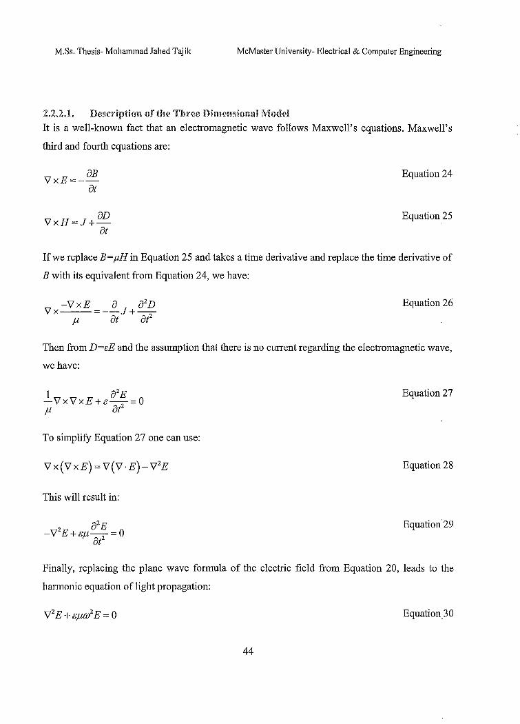
M.Ss. Thesis- Mohammad lahed Tajik McMaster University- Electrical & Computer Engineering
2.2.2.1. Description of the Three DimeHsionllllVlodel
It is a well-known fact that an electromagnetic wave follows Maxwell's equations. Maxwell's
third and fourth equations are:
aB \1xE=--at
aD \1xH=J+at
Equation 24
Equation 25
If we replace B=/lH in Equation 25 and takes a time derivative and replace the time derivative of
B with its equivalent from Equation 24, we have:
Equation 26
Then from D=eE and the assumption that there is no current regarding the electromagnetic wave,
we have:
1 a2E -\1x\1xE+£-2-=0 Ji at
Equation 27
To simplify Equation 27 one can use:
Equation 28
This will result in:
Equation'29
Finally, replacing the plane wave formula of the electric field from Equation 20, leads to the
harmonic equation of light propagation:
Equation 3 0
44
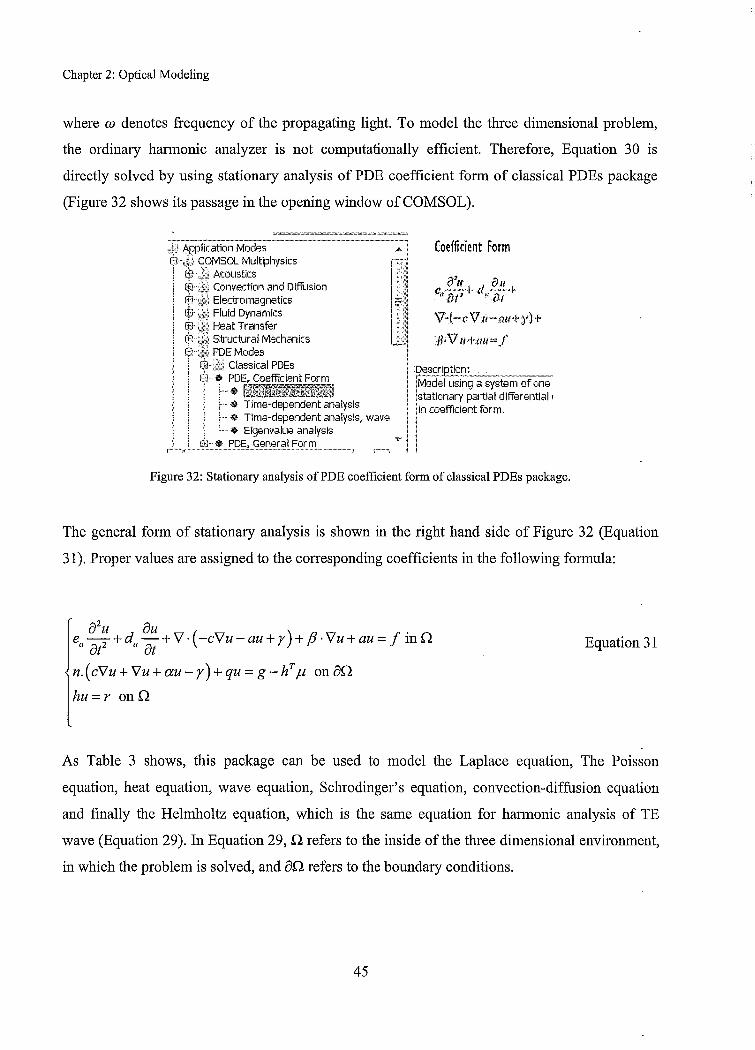
Chapter 2: Optical Modeling
where w denotes frequency of the propagating light. To model the three dimensional problem,
the ordinary harmonic analyzer is not computationally efficient. Therefore, Equation 30 is
directly solved by using stationary analysis of PDE coefficient form of classical PDEs package
(Figure 32 shows its passage in the opening window of COM SOL).
.. U Application Modes A :
i~'Jk; COMSOL Multiphysics f;;~': l m-:, Acoustics j--- $ .. :JJ Convection and DiffLlsion Ii
(tj· ;1; Electromagnetics ! i; $'\},; Fluid Dynamics 11_ .... $f'J} Heat Transfer E~l if;;; Structural Meehan ies S,,~ PDE Modes i [j:J.,{; Classical PDEs
l+l". PDE, Coeftkient Form
I [': ~:~~:~!~;:~!:::;:::¥ wave I : : .... ,. Eigenvalule analysis "...1 fi}·. PDE, Genera Form , ... -----1>---.. --...... -.. -----.... --.................. -...... _ .. _ ...... _ .... _ .. _ .... _-_ .. __ .. - ............... j. ! .......... "!
Coefficient Form
fJ'f1 011 e----+ d ----+ " 0(' " tJl
\7-(-c" 1I"~awl'Y)+
11:V 1/""'111 '" f
Des~~ip.!!i:!.r:t_: ______ _ jModel using a system of one jstationary partial differential, jin coefficient form.
Figure 32: Stationary analysis ofPDE coefficient form of classical PDEs package.
The general form of stationary analysis is shown in the right hand side of Figure 32 (Equation
31). Proper values are assigned to the corresponding coefficients in the following formula:
a2u au ( ) . ea - 2 +da -+ Y'. -cY'u-au+r + fJ· Y'u+au= f mn at at Equation 31
n. (cY'u + Y'u + au - r) + qu = g - hT J1 on an hu=r onn
As Table 3 shows, this package can be used to model the Laplace equation, The Poisson
equation, heat equation, wave equation, Schrodinger's equation, convection-diffusion equation
and finally the Helmholtz equation, which is the same equation for harmonic analysis of TE
wave (Equation 29). In Equation 29, n refers to the inside of the three dimensional environment,
in which the problem is solved, and an refers to the boundary conditions.
45

M.Ss. Thesis- Mohammad Jahed Tajik McMaster University- Electrical & Computer Engineering
Table 3: The Plethora of equations that can be modeled via PDE coefficient form (stationary analysis). EQUATION COMPACT NOTATION STANDARD NOTATION
Laplace -v ·(Vu) = 0 oou oou oou _ 0 equation
----------oxox ayoy ozoz
Poisson -V· (cVu) =0 -~(c ou )-~(c ou )-~(c ou) =! equation ox ox ay oy oz oz
Helmholtz -V . (cVu) +au =! -~(c ou )-~(c ou )-~(c ou )+au =! equation ox ox By By OZ OZ
Heat au d ou _~(cou)_~(cou)_~(cau)=! equation d - - V . ( cVu ) = !
a ot a ot ox ax By oy az az
Wave 02U d 02U _~( C ou )-~(c ou )-~(c au) =! equation d --V.(cVu)=!
a ot2 a aP ox ox oy oy az oz
Schrodinger -V . (cVu) +au = AU -~(couJ-~(couJ-~(cou)+au=Au equation ox,ox/ Oy, Oy/ OZ OZ
Convection- ou d au -~(c au )-~(c au )-~(c au)+,B au +,B au = diffusion d --V.(cVu)+j3.Vu=!
a ot Qat ax ax ay ay az az xax Yay J
equation
Table 4 shows how to choose values of the corresponding coefficient to model the Helmholtz
problem.
T bl 4 P a e arameters va ues £ or generatmg e . 0 tz s equatI Hlmhl' on. Parameter Quantity
p 0
'Y 0
a 0
a 811m;!
ea 0
da 0
f 0
c -1
46

Chapter 2: Optical Modeling
After assigning proper values to the parameters, the next step is to take care of the boundary
conditions. The general equations of boundary conditions for an electromagnetic wave in all
sorts of environments are shown in Table 5.
Two types of boundary conditions are included III the PDE package: Dirichlet boundary
condition and Neumann boundary condition.
n· (cVu + au - r) + qu = g Equation 32
n· (cVu + au - r) + qu = g - hT J1; hu = r EquationJ3
Equation 32 shows the Neumann boundary conditions at the border. The only undefined
parameters in this equation are q and g. The rest of the parameters have already been defined by
defining the model of the Helmholtz's equation. Consequently, Equation 33 shows the Dirichlet
boundary conditions. Similar to Equation 32; parameters in Equation 33 are all defined except
for q, g, h, rand f1 which denotes the magnetic permeability.
a e T bl 5 G enera oun ary can I Ions, I b d d't' or e ectromagnetlc waves Finite conductivity Medium of infinite electric Medium of infinite media, no source or conductivity Magnetic conductivity
charges 0"1 =00;0"2 :f:=oo;Ms =O;qm.r =0 (H =O)J =O'q =0 II .r' es
General 0',,0'2 *00
Js = Ms =O;q", =qn~ =0
Tangential electric field
intensity ii x ( E2 - EI) = - M ii x (E2 - EI) = 0 n XE2 =0 RxE2 =-M
Tangential magnetic field
intensity ii X(H2 -HI) = -J. fix(H2 -HI)=O iixH2 =J. RxH2 =0
Normal electric flux density
fi.(D2 -DI) = -qes R.(D2 -DI)=O RD2 = qes fiD2 = 0
Normal electric magnetic flux
density ii.( B2 - BI) = -qms Ii. (B2 - BI) = 0 n.B2 =0 n.B2 =q",.
47

M.Ss. Thesis- Mohammad Jahed Tajik McMaster University- Electrical & Computer Engineering
Table 6 shows the mentioned boundary conditions and the proper definition of coefficients. Now
that everything is completed the next step is to properly run the described model. There are two
ways to do this:
Using equivalent M-file for the model by connecting to MATLAB server (by following
this path: File/Clienet-serverIMATLAB) and then saving the model as an M-file. Next,
by defining a for-loop on wavelength and changing all the parameters based on their
wavelength equivalents and then getting an integral on electric field magnitude, the
model will be completed.
Instead of stationary analysis and then use of MATLAB platform, parametric analysis
can also be used by defining wavelength as the changing parameter, just like the two
dimensional section.
a e T bl 6 Ch oosmg 0 : parameters 0 genera e f t th e nee e oun ary con lhons. d db d d" Finite conductivity media, no
source or charges Medium of infinite Source
0'1'0'2 oF 00 electric conductivity
J s = Ms = 0; ges = g,ns = 0 0', = 00;0'2 *oo;Ms = O;q.u = 0
Dirichlet boundary g = 0, q = 0, h = 0, r = ° g=l,q=O,h=l,r=O g = l,q =O,h =l,r=l
condition
Neumann g=O,q=O g = l,q = 0 g = l,q = a boundary condition
In a typical solar cell, the required electromagnetic boundary conditions are:
the boundary condition between two layers with finite electrical conductivity with no
charge and source of light
interface of semiconductor and metal (or medium with close to infinite electric
conductivity)
source of light
48

Chapter 2: Optical Modeling
2.2.2.2. 'Ihree l)imcnsiomd l'v.todd. Results and Discussion
In both of the mentioned methods, all of the changing parameters such as complex refractive
indices and the source of light should be considered as a function of wavelength (by following
this path: Options/Functions). Figure 33 shows the result of a simple two layered device inside a
bigger box that models the environment (air condition with electrical permittivity and magnetic
permeability equal to one).
Using parameters in Table 6 the top face of the outer box is designed to be the source of light
with magnitude one, which is represented by the red color at the top of the box. The blue color in
the middle of the picture has the largest light intensity, which is calculated as IE21. This is the
inverse of quantum well concept for electron wave in Schrodinger's equation. In the case of
quantum well, the electron wave has the highest magnitude inside the well. For solution of light
propagation in an environment with different refractive indices, light will be trapped inside the
materials with higher refractive indices. Figure 34 shows a quantum well besides a light trapping
specimen (this technique oflight trapping is extensively used in fiber optics [39,40])
,-________ -"'-!!!." ________ ---, MKI~,",
. ..,
Figure 33: results of a simple three dimensional two layered structure
49
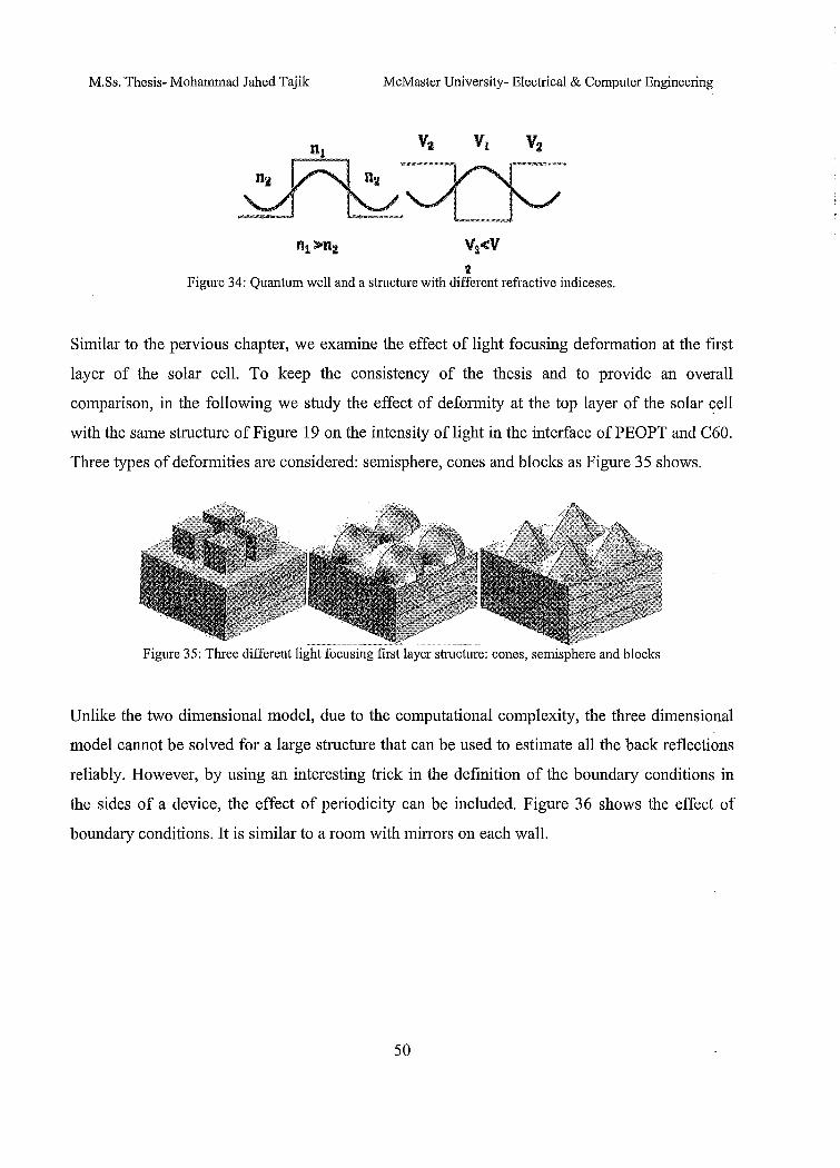
M.Ss. Thesis- Mohammad Jahed Tajik McMaster University- Electrical & Computer Engineering
a Figure 34: Quantum well and a structure with different refractive indiceses.
Similar to the pervious chapter, we examine the effect of light focusing deformation at the fIrst
layer of the solar cell. To keep the consistency of the thesis and to provide an overall
comparison, in the following we study the effect of deformity at the top layer of the solar cell
with the same structure of Figure 19 on the intensity oflight in the interface ofPEOPT and C60.
Three types of deformities are considered: semisphere, cones and blocks as Figure 35 shows.
Figure 35: Three different light focusing first layer structure: cones, semisphere and blocks
Unlike the two dimensional model, due to the computational complexity, the three dimensional
model cannot be solved for a large structure that can be used to estimate all the back reflections
reliably. However, by using an interesting trick in the defInition of the boundary conditions in
the sides of a device, the effect of periodicity can be included. Figure 36 shows the effect of
boundary conditions. It is similar to a room with mirrors on each wall.
50

Chapter 2: Optical Modeling
a--.. - ~~
§ '\
If '-I ,
II II
, \
Figure 36: Concept of mirror boundary condition with a real source of light in the middle and two imaginary sources oflight in its right and left. (imaginary rays are represented by doted lines).
This type of boundary condition is similar to the situation that two mirrors are facing each other.
In Figure 36, two beams oflight are depicted by two lines (blue line in the left and red line in the
right). As shown in the picture, there is one real source oflight with real beams oflight (solid
lines) and two imaginary sources of light in the left and right of the real source (doted lines). As
it is shown in the picture, if everything is symmetric inside and outside of the solar cell, mirror
boundary will model the effect of a device with infinite width.
Similar to the previous section, the magnitude of electrical field for different designs by using the
model described in here with all of the refractive indices from Figure 16, is calculated and
depicted in Figure 37, Figure 38 and Figure 39.
51
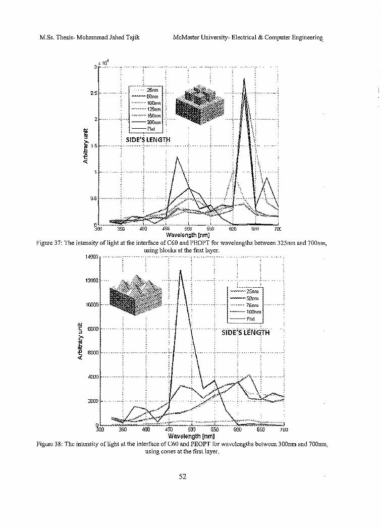
M.Ss. Thesis- Mohammad Jahed Tajik McMaster University- Electrical & Computer Engineering.
250m --SOnl11 •••• -·.ee> 100nro
-.. -. -·125n!'!l "~. ~ .. ~. 1£\Onll1 • --200nm T"" --Flat ~
.. . SIDE'S LENGT)i
,.".-~. >,. >~":<. > <~. ,~ •. o, .~<~. > <~:, _, <,-,',:-:
I. ....
o~~~~~~.r:= 3m 350 A50 SOD 550 600 70[
Wavelength [hm} Figure 37: The intensity oflight at the interface ofC60 and PEOPT for wavelengths between 325nm and 700nm,
using blocks at the first layer. ·14000 ........... : ............ : .............. ; ........... ~ ............. : ............ ; ............ : ............. :
12000 .".
10000 -
2000··· .. , ..
'" . . -'.. ~ · . · . · .
5"...0 Wavelength [nm]
." .- •. -;-< ... - ...... --: . . r--'----'--=~~. ,
-. -.. -. ·-·50nrn 750m I·"
-l00nm -Flat
650 700
Figure 38: The intensity of light at the interface of C60 and PEOPT for wavelengths between 300nm and 700nm, using cones at the first layer.
52

Chapter 2: Optical Modeling
RADIUS
I(O"J(} ~ ...
n_. _____ ~ ____ ~~~~~--~~--~i~--~~==~~--~ ~ 400 SOO 5I'.J.l 700
Wavelength [om] Figure 39: The intensity oflight at the interface ofC60 and PEOPT for wavelengths between 300nm and 700nm,
using spheres at the first layer.
Finally, all of the results are summarized in Table 7. Description of each column is the same as
Table 6. It can be concluded that the best design is for the case of usage of blocks with the scale
of 150nm. In general comparison with the results of two dimensional light focusing apertures
reveals that the best design is the semicylindricals with radius equal to 125nm increases the
amount of absorbed power compared to the flat surface case by 98%.
The next step in modeling is to use the calculated amount of absorbed power to find the density
of generated excitons. To do so, we assumed that for the wavelengths larger than the active
layers' bandgap, (for the exchange efficiency=l), the number of excitons for each wavelength
can be calculated using the following formula:
Q(x,m) # excito ns = --'---'-I
Equation 34
hm
53

M.Ss. Thesis- Mohammad Jahed Tajik McMaster University- Electrical & Computer Engineering
Having the number of excitons, the amount of generated electrical current can be obtained. This
topic is explained in details in the next chapter.
Table 7: Results of the simulation for the a~,,,'~"'~"O normalized to the flat surface results
Total optical absorption in absorption in Total Power PEOPT e60 absorption
Block 25nm
Block50nm
Block lOOnm
Block 125nm
B1ock150nm
BIock200nm
cone 25nm
cone50nm
cone 75nm
cone lOOnm
Sphere50nm
Sphere 75nm
54

Chapter 3: Electrical Modeling
CHAPTER 3
ELECTRICAL MODELING
3. ELECTRICAL MODELING
In this section, the electrical model for two types of organic solar cells (bilayer heterojunction
and bulk heterojunction organic solar cells) is described. One of the important characteristics of
organic materials is their extremely small mobility, which makes modeling of their electrical
properties difficult. However, as was mentioned before, we used COMSOL multiphysics that
employs FEM as its descritization method, which is a stable numerical method. Benefiting
adaptive feedback and adaptive meshing properties of COMSOL the modeling becomes more
stable and efficient.
Another problem in the electrical modeling of organic thin film devices (e. g. planar organic
solar cells) was the lack of unique and precise electrical parameters for very thin layers of
materials and occasionally lack of any information. For instance, Indium Thin Oxide's (ITO)
parameters which are reported below (ITO is one of the usual materials in most of planar solar
cells and especially organic solar cells) is a perfect example. Table 8 shows the differences
between the ITO parameters reported from different references.
The first section of this chapter is dedicated to the analytical solution of the exciton diffusion
equation which is related to the bilayer heterojunctions. In this model, it is assumed that a
fraction of excitons that can reach the interface of active layers, and get separated into pairs. of
electron and holes, will generate the short circuit current of the organic solar cell. Later, it will be
described how IPCE of the organic solar cell can be calculated, using the calculated short circuit
current.
In the next section, the electrical model of bulk heterojunction organic solar cell is described,
using COMSOL multiphysics software. In this section, with the aid of a self consistent loop
55
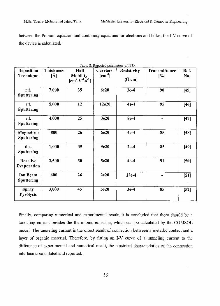
M.Ss. Thesis- Mohammad Jahed Tajik McMaster University- Electrical & Computer Engineering
between the Poisson equation and continuity equations for electrons and holes, the I-Y curve of
the device is calculated.
bl d Ta e 8: R~orte . parameters ofITO.
Deposition Thickness Hall Carriers Resistivity Transmittance Ref. Technique [A] Mobility [cm-3] [%] No.
[cm2.y-l.s-l] [O.cm]
r.f. 7,000 35 6e20 3e-4 90 [45] Sputtering
r.f. 5,000 12 12e20 4e-4 95 [46] Sputtering
r.f. 4,000 25 3e20 8e-4 - [47] Sputtering
Magnetron 800 26 6e20 4e-4 85 [48] Sputtering
d.c. 1,000 35 ge20 2e-4 85 [49] Sputtering
Reactive 2,500 30 5e20 4e-4 91 [50] Evaporation
Ion Beam 600 26 2e20 12e-4 - [51] Sputtering
Spray 3,000 45 5e20 3e-4 85 [52] Pyrolysis
Finally, comparing numerical and experimental result, it is concluded that there should be a
tunneling current besides the thermionic emission, which can be calculated by the COMSQL
model. The tunneling current is the direct result of connection between a metallic contact and a
layer of organic material. Therefore, by fitting an I-V curve of a tunneling current to the
difference of experimental and numerical result, the electrical characteristics of the connection
interface is calculated and reported.
56

Chapter 3: Electrical Modeling
3.1. I:U~C'rIUCAL MODELl ANALYTICAL ANALYSES
The next part of the modeling is to calculate the optical current generated in the solar cell. To do
so, the excitons distribution equation as a function of position and light intensity will be found. by
assuming that the exciton separation into electron-hole pare only happens in the interface of n
type and p-type materials, the short-circuit current can be calculated, and from there, IPCE can
be found.
3.1.1. EXCITON DIFFUSION EQUATION
3.1.1.1. nt~s\~ription of the Exciton Diffusion Model
Number of references solved the problem of exciton diffusion (assuming that after excitation the
number of excitons follows the profile oflight distribution) as [21-26]:
Equation· 35
Equation 35 implies that S(x) (the number of excitons) will decay by an exponential function of
distance (x) from the incident point. However, the reality is that the excitons, like any other
particle, diffuse into their neighbourhood. Therefore, assuming that the total change in the
number of excitons (n(x)) at the point x (distance from the sight of the excitation), is due. to
diffusion and decay, the equation for exciton density become:
Equation 36
In this equation, Q(x) is the absorbed energy which has been calculated in the previous section, D
is the diffusion constant, r is the mean lifetime of the exciton, fh is the exciton exchange
efficiency and hv is the creation energy of an exciton where v stands for the frequency of the
absorbed light.
Knowing the classical PDE equation, one can conclude that Equation 36 is the diffusion equation
for excitons (where excitons are taken as the diffusive particles inside the device), and like any
diffusion equation, it consists of three terms:
57

M.Ss. Thesis- Mohammad Jahed Tajik McMaster University- Electrical & Computer Engineering
The diffusion term (due to uneven absorption oflight)
The dissipation term (due to dissociated excitons)
The generation term (due to optical generation of excitons).
For the steady state situation (Where the time derivative of n is zero), Equation 36 can be
rewritten as:
Equation 37
In the above equation fJ is the inverse of the exciton diffusion length:
Equation 38
Using analytical solution of the Equation 37, n(x) would have an exponential form as:
n (x) = B1aTN [A.e- fJX + B.efJx + C .eax + C . cos (47r17 (d - x) + 5 11)]
D(fJ2 _a2) 1 2 A
Equation 39
In the above equation N stands for the number of photons per unit area, the coefficient (6") is the
argument of the complex reflection coefficient that have been calculated in the TM section and
C] and C2 are defmed as below:
Equation 40
Equation 41
Therefore, only A and B from Equation 39 are unknown. To find these two unknowns, the
boundary conditions should be applied. Assuming that excitons either decay during the diffusion
or totally dissociate at the interface, the total number of excitons at the boundaries should be
equal to zero (n(x) =0 at the boundaries). Therefore, substituting the boundary conditions. in
58
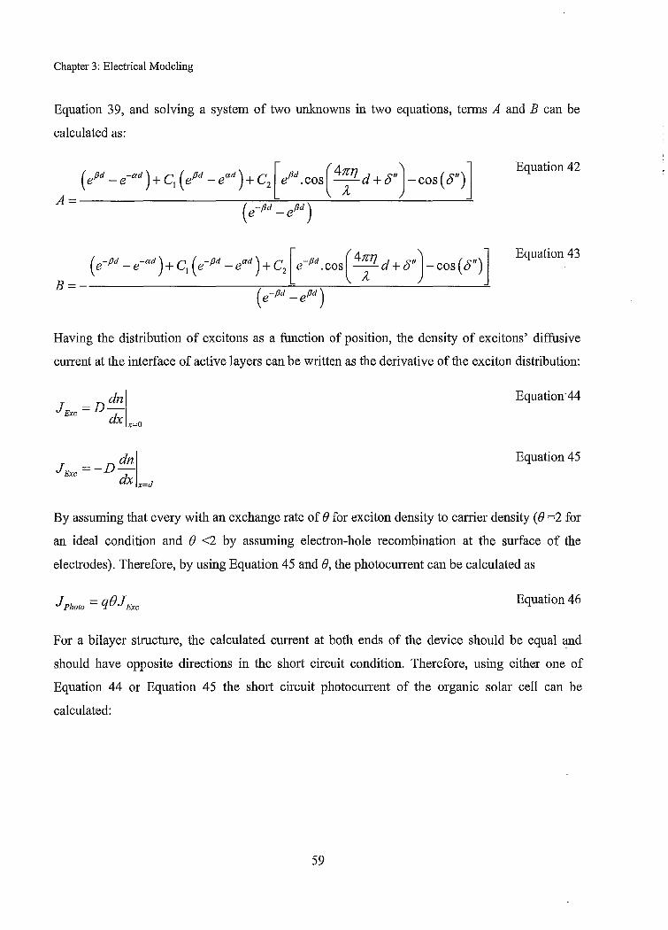
Chapter 3: Electrical Modeling
Equation 39, and solving a system of two unknowns in two equations, tenns A and B can be
calculated as:
(epa _e-aa )+ C1 (epa - eaa )+ C, [ePd.cos( ~d + 5" )-COS(5")]
A= (e-Pd_ePd )
Equation 42
B= (e-Pd _e-aa )+ C1 (e- pa _ead )+ C, [e-Pd.cos( ~d + 5") - cost 5")]
(e-Pd_ePd )
Equation 43
Having the distribution of excitons as a function of position, the density of excitons' diffusive
current at the interface of active layers can be written as the derivative of the exciton distribution:
T _ n dn J Exc =u-
dx x=o
J Exc = -D dnl dx x=d
Equation-44
Equation 45
By assuming that every with an exchange rate of e for exciton density to carrier density (e =2 for
an ideal condition and e <2 by assuming electron-hole recombination at the surface of the
electrodes). Therefore, by using Equation 45 and e, the photo current can be calculated as
Equation 46
For a bilayer structure, the calculated current at both ends of the device should be equal ~nd
should have opposite directions in the short circuit condition. Therefore, using either one of
Equation 44 or Equation 45 the short circuit photo current of the organic solar cell can be
calculated:
59

M.Ss. Thesis- Mohammad Jahed Tajik McMaster University- Electrical & Computer Engineering
I qf)aTN ( -Pd pd -ad JpllOIOX=d = (fJ2_
a2) fJA·e -fJB·e +a·e
Equation 47
+aCl • ead - 4~7J C2 • sin [ 5"])
3.1.1.2. Exciton Diffusion EClulltion Results and Discussion:
One way of fmding efficiency of a solar cell is to divide the calculated current by the incident of
monochromatic photon stream which (or shortly !PCE) [28]:
1PCE(%) = 1240x Jpholo
A10
Equation 48
In the above equation, Jphoto (1-IA/cm2) is the calculated photo current, A is the wavelength (nm)
and 10 is the light intensity (W/m2). The !PCE for the first device was calculated for 16 different
wavelengths (400nm-7000nm). A schematic model of the organic solar cell's structure shown in
Figure 40 and has the following characteristics: 1 mm thick layer of glass, 120nm ITO, 110 nm
PEDOT, 40 nm PEOPT and 31 nm C60. Using trial and error, the best fit with the measurement
is obtained for diffusion lengths equal to 6nm and 7nm for PEOPT and C60 respectively (Figure
41).
Figure 40: The structure of the solar cell that has been modeled in this section [28].
60
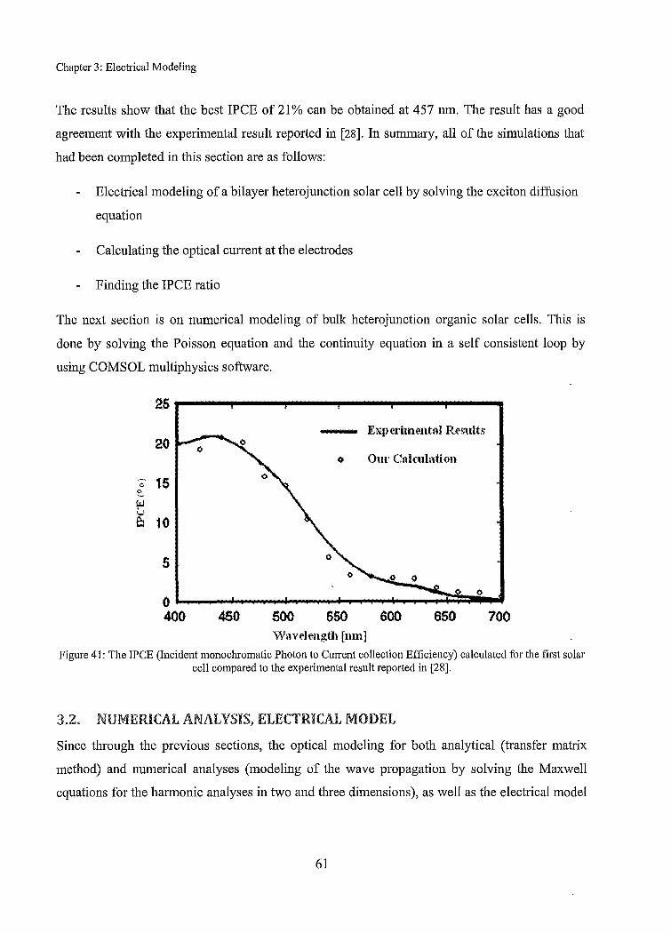
Chapter 3: Electrical Modeling
The results show that the best IPCE of 21 % can be obtained at 457 nm. The result has a good
agreement with the experimental result reported in [28]. In summary, all of the simulations that
had been completed in this section are as follows:
Electrical modeling of a bilayer heterojunction solar cell by solving the exciton diffusion
equation
Calculating the optical current at the electrodes
Finding the IPCE ratio
The next section is on numerical modeling of bulk heterojunction organic solar cells. This is
done by solving the Poisson equation and the continuity equation in a self consistent loop by
using COMSOL multiphysics software.
25 ,
EX(>(>l'imentnl R(>Slilts 20
o OUI' Calculation
" 15 ~
~ \,,: e 10
5
()
0 400 450 500 650 600 650 700
'Vavelength [mn]
Figure 41: The IPCE (Incident monochromatic Photon to Current collection Efficiency) calculated for the first solar cell compared to the experimental result reported in [28].
3.2. NUMERICAL ANALYSIS, ELECTRICAL MODEL
Since through the previous sections, the optical modeling for both analytical (transfer matrix
method) and numerical analyses (modeling of the wave propagation by solving the Maxwell
equations for the harmonic analyses in two and three dimensions), as well as the electrical model
61

M.Ss. Thesis- Mohammad Iahed Tajik McMaster University- Electrical & Computer Engineering
of bilayer heterojunction organic solar cells were discussed, this section deals with electrical
modeling of bulk heterojunction organic solar cells to complete the modeling of solar cells.
It is assumed that the electrical current is due to the drift-diffusion transport of carrier.
Consequently, in order to model the drift diffusion equations, a self consistent loop between the
solutions of Poisson's equation and two separate continuity equations for electrons and holes is
needed. The design of the loop should be in a way such that the solution of each equation can be
used as the initial conditions for the others, to generate a self correcting mechanism.
In order to check the accuracy of the model, results are compared with the numerical results
reported in [41] for different doping concentration in the active region. Later, at the end of this
section, results are also been compared to the experimental result. It will be shown that the
numerical and experimental results have dissimilarity. In order to describe this difference, the
tunneling correction is introduced in the next section.
3.2.1. DRIFT-DIFFUSION MODEL
3.2.1.1. Description of the Drin-nitIm~jon l\'lodeL In this section, a bulk heterojunction organic solar cell (OSC) is chosen to be modeled. The bulk
heterojunction OSC is a solar cell that has both n- and p-type materials as a mixture in the same
layer. From this point, we will call this layer the "active layer" or "active region".
As was described before, the bulk heterojunction structure and the fact that mixing n-type and p
type materials in the same layer would dramatically increase the chance of converting an exciton
into a pair of a free electron and hole, leading to a 5 to 7% increase in the efficiency of the
device. Figure 42 shows the band diagram of a bulk heterojunction organic solar cell (BROSC).
The properties of a planar BROSC with its band diagram shown in Figure 42 are as follows: a
standard ITO substrate covered by glass, covered by a 40nrn thick layer of poly (3, 4
ethylenedioxythiophene) mixed with poly (styrenesulfonate) which also can be called by the
abbreviation "PEDOT: PSS". PEDOT: PSS layer is the spacer which is located between the
active region to prevent excitons from clinching in the interface of electrode and the active layer.
62

Chapter 3: Electrical Modeling
In the case of the active layer interface with the metallic electrode a very thin layer of the active
layer will be depleted due to electrochemical phenomena happening at the metal-organic
interface (this will be discussed in more details in the final section) which can act as a spacer
[42].
_AI ;) I . / ph«"
~-..£~""'~1 ~h' C...... .....;1~rO_ P3HT PED01YPSS
PCBM
Figure 42: The band diagram of a bulk heterojunction OSc.
The next layer is called the active layer and is composed of Poly(3-hexylthiophene) (P3HT) and
[6,6]-phenyl C61-butyric acid methyl ester (PCBM) with a ratio of 3:2wt. The reason to choose
these materials is that using them, some of the most efficient organic solar cells can be fabricated
[43].
In this combination P3HT, has the most absorption of light (because of bigger imaginary
components in its refractive indices for the higher wavelengths) and therefore higher rate of
exciton generation, but PCBM have a higher mobility. Therefore while the P3HT islands are
absorbing most of the light and generating excitons, the PCBM around them act as an electron
collecting network. This device is fabricated by M. Glatthaar et al. [41]. They used spin coating
of3:2wt solution ofP3HT and PCBM from O-dichlorobenzene solution to deposit an 80nm thick
layer. Finally, the last layer is a 100nm thick layer of Aluminum (AI), which is deposited with a
rate of 2 nm/s, under 1 x 1 0-3 Pa via vapour deposition.
For the electrical model, because of simplicity in the geometry which represents a one
dimensional (lD) electrical problem, a ID model would be sufficient. Therefore, the following is
a description of a ID COMSOL multiphysics model for a self consistent loop between a ID
Poisson equation and two sets of a ID continuity equations for electrons and holes separately, as:
-'l.&'lV = q(p -n) Equation 49
63

M.Ss. Thesis- Mohammad Jahed Tajik McMaster University- Electrical & Computer Engineering
V.(-DnVn + nPnE ) = G-R
V.(Dp Vp+ pppE) = G-R
The model that is used is based on the following assumptions:
Equation-50
Equation 51
The generated excitons are separated right after absorption inside the active region and
the numbers of the generated electron-hole pairs are directly imported into the continuity
equations as the generation rate (G in Equation 50 and Equation 51).
The transport properties of the organic materials can be totally modeled by mobility,
DOS, bimolecular recombination term and doping levels.
The connections between different layers follow the physical rules of heterojunction
connections between conventional semiconductors interfaces.
In the first step, the Poisson equation (Equation 49) is solved. For the first iteration, the
distribution of charges can be found from the equations:
E q'f/+%+---.!L
2 kT
kT
The boundary conditions for the Poisson equation are:
Continuity in internal boundaries (organic layers interfaces with each other)
Equation 52
Equation 53
Fixed potentials at the interface of organic materials and electrodes, follow the ohmic
connection condition:
64

Chapter 3: Electrical Modeling
Ndop;ng + 2 Equation 54
In Equation 54, Va is the applied voltage at the contacts, EG is the active layer's bandgap, Ndoping
is the dopands density and ni is the intrinsic carrier density.
Two different COMSOL's packages were used to solve the Poisson equation:
PDE coefficient fonn, stationary analyses package (the one that have been used for the
three dimensional solution of wave propagation)
Classical PDE, Direct Poisson solver
Both of the mentioned packages have the same result, and for our case none of them has any
processing advantage over the other one (Figure 43).
SpiKe dimension;
'~i; ~pplication Modes tJ .. ~#) COMSOL MuJtiphysics , (tlJ!) Convection and Diffusion
tj}";J,j Heat Transfer It''~M POE Modes , $·JI, Classical PDt:s
j t··· @ Convection-Diffusion Equation 1 ,... Heat Equation
[ .. @ Helmh'Jltz Equation .@
i l..... Wave Equation l~ .. ~ POE, Coefficient Form l 1"" Stationary analysis
, i ;.. til Time-dependent analvsis
( li;;;;~;,.";",;",,,;;;::i,IL::'i";I;@~ti,",,,j"i.,,,,,j,;:,,,,,;~,,,-J __ ~_. --'
Classical PDEs
• fYli.l.. {Gil .. tid 0/' • (., Of I
V·{o-a V (/-au+y)+
I{' 'Vu+mi c /'
[)escr iP-~£!l.L Poisson's equation,
Figure 43: Depiction of the Poisson equation package root in the first window of the COMSOL simulator for the one
65
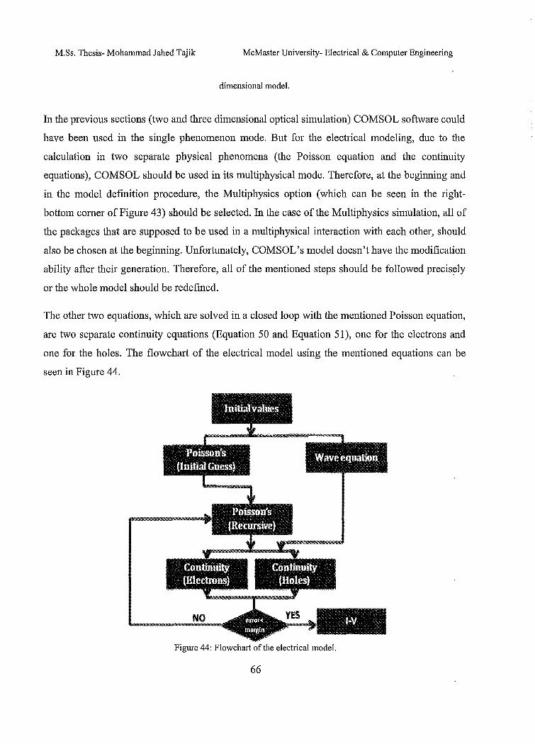
M.Ss. Thesis- Mohammad Jahed Tajik McMaster University- Electrical & Computer Engineering
dimensional model.
In the previous sections (two and three dimensional optical simulation) COMSOL software could
have been used in the single phenomenon mode. But for the electrical modeling, due to the
calculation in two separate physical phenomena (the Poisson equation and the continuity
equations), COMSOL should be used in its multiphysical mode. Therefore, at the beginning and
in the model definition procedure, the Multiphysics option (which can be seen in the right
bottom comer of Figure 43) should be selected. In the case of the Multiphysics simulation, all of
the packages that are supposed to be used in a multiphysical interaction with each other, should
also be chosen at the beginning. Unfortunately, COMSOL's model doesn't have the modification
ability after their generation. Therefore, all of the mentioned steps should be followed precisely
or the whole model should be redefined.
The other two equations, which are solved in a closed loop with the mentioned Poisson equation,
are two separate continuity equations (Equation 50 and Equation 51), one for the electrons and
one for the holes. The flowchart of the electrical model using the mentioned equations can be
seen in Figure 44.
~
Initial values
Continuity (IDectnms)
"
~" ,,, v '"" ~
Wave equation
I"V
Figure 44: Flowchart of the electrical model.
66

Chapter 3: Electrical Modeling
As it can be seen in Figure 44, there are two Poisson equation solvers. The only difference
between these Poisson solvers is their initial conditions. As was mentioned before, getting
convergence in a closed loop of the Poisson equation and continuity equation, when the modeled
semiconductor has characteristics similar to the characteristics of organic materials, is really hard
and needs lots of iterations. Therefore, having a correct initial value will reduce the number of
iterations.
The goal of having the first Poisson equation is to provide an efficient guess for initial value of
voltage at any point in the device for the second Poisson solver. However, its own initial value is
assumed to be defined by the following equation:
V;nit = ~(-log(Pinit/ni)x (NdoPing < 0) ...
+ 10g(ninu/n;) x (NdoPing >=O))-X -0.5xEg Equation 55
In the Equation 55, V;=(q/kT) is the thermal voltage, Eg is the bandgap, Xis the electron affinity
and Ndoping is the doping concentration. Also, pinit and ninit stand for charge concentrations at the
interfaces of the active layer and the electrodes, which can be calculated from the following
equations:
nini( = (INdOPingl/2+~(N~oPing /4+ n/))x(NdoPing >= 0) ...
+ n/ / (I NdoPing 1/2 + ~(N~oPing /4+ n/))x (NdoPing < 0) Equation 56
Pinit = (INdOPingl/2+~(N~oPing / 4+n/))x(NdoPing < 0) ...
+ n/ / (INdOPingl/2+~(N~oPing / 4+n/))x (NdoPing >= 0) Equation 57
Here, the doping concentration concept is slightly different than conventional semiconductors. In
both cases the doping concentration and the Fermi level have a close relationship. In
conventional semiconductors, the Fermi's level moves up or down by increasing or decreasing
the number of electrons. The same rule is true for organic semiconductors, except that instead of
adding a new material as the dopant to change the intrinsic balance of carriers, this change can be
67

M.Ss. Thesis- Mohammad Iahed Tajik McMaster University- Electrical & Computer Engineering
obtained by change in the weight ratio [53] or in the synthesis temperature [54] or the annealing
time [55, 56].
The next section is to model the continuity equations (Equation 50 and Equation 51). The
package that is going to be used for this section is the steady-state analysis of convection and
diffusion, shown in Figure 45.
'~~\MQ~~I~~~i~~!~EC' . Ne'w i;!~lgH~L~J!l§lPyJ~h{~~~'IY.!'9f!'81%~H~;fi"§~~1r:l~~ .................................................................................. _ ... _ ..... _._ .............................................. ,
Space dimension:
";j1 Application Modes ! !till COMSOL Multiphysics ! i Fp'''}{~ Convection and DiffiJsion
il E)"~Co
Heat Transfer Pr1F MnrlAf'>
Convection and Diffusion
Figure 45: Picture of Steady-state analysis of convection and diffusion at the opening window of COMSOL. .
It was assumed that the electrons and holes have separate continuity equations with the same
generation (G) and recombination rate (R). G comes from the optical section and R is calculated
via bimolecular recombination term [41]:
R = f3n ( x ) p ( x ) Equation.58
In Equation 50 and Equation 51, fl-n and fl-p stand for the electron and hole mobilities. Also Dn
and Dp refer to carrier diffusivities which can be defined as below:
Dn1p = V; X f.inl p Equation 59
The boundary conditions for the continuity equations are defined by Equation 56 and Equation
57. Charge densities initial values are also defined by Equation 52 and Equation 53. Having
defined all of the mentioned in the scalar expression window in COMSOL Multiphysics, it is
time to define the rest of the required coefficients (Table 9).
68

Chapter 3: Electrical Modeling
Having all of the parameters and boundary conditions properly defined, it is necessary to define
the modeling algorithm using MATLAB coding or solving script inside the COMSOL Solver
Manager. The algorithm shown in Figure 44 can be seen through the following script:
"init = asseminit(fem};
fem.sol=femstatic(fem, ...
'init',init, ...
'solcomp',{'phiO'l, ...
'outcomp',{ 'phiO'}, ...
'maxiter ',250000000};
femO=fem;
init = asseminit(fem,!em{).sol);
fem.sol=femstatic(fem, ...
'init',init, ...
femO.sol, ...
'solcomp ',{'1m3 " 'phi', 'pc', 'nc', 'Im4'l, .. .
'outcomp ',{'1m3 " 'phi', 'pc', 'Im4', 'nc'l, .. .
'pname', 'Vd', ...
'plist',[-1.3:0.005:-1.2 -1.19:0.01:0 0.02:0.02:0.6 O. 65:0. 05:1. 6J, ...
'maxiter',250000000, ...
'hnlin', 'on?;
femO=fem ";
In the first part of the above script (femO=fem), the first line:
"init = asseminit(fem};"
assigns the initial values to the information that have been already provided trough the constant
window and the scalar expression window. The second line is the beginning of static analyses.
The third line calls the initial values and the forth line defmes set of equations that should. be
69

M.Ss. Thesis- Mohammad Jahed Tajik McMaster University- Electrical & Computer Engineering
solved. At this point, it will solve ''phiO'', which stands for the name of the first Poisson's
equation variable. The first Poisson equation is going to be solved to give an adequate first guess
for the second Poisson equation's initial value.
T bl 9 P a e arame ers a ave th th b d' F' een use III 19ure 46
Models OurCOMSOL Glatthaar & et. al. Model
Parameters [41]
Density of states 4x1020 cm-3 5xI02°cm-3
Electron and hole mobility 1x10⁻⁴ cm-:t/(V.s) Ix10-4 cm-:t/(V.s)
2xI016 cm-3, 8xI016 Ix1 016 cm-3
, 4x1 016
cm-3, 2.4x1017 cm-3 cm-3, 1.6xI017 cm-3
p-doping level
Dielectric constant 3.8 3.8
active region's LUMO (PCBM's LUMO) 4.3 eV 4.3 eV
active region's HOMO (P3HT's HOMO) 5.2eV 5.2 eV
Contact work function for the n-contact (Cathode) 4.1 eV 4.1 eV
Contact work function for the p-contact (Anode) 5.0eV 5.0eV
The next line stands for the variable that is going to be reported in the output. The sixth line
shows the maximum number of iterations before reaching convergence with the default error
smaller than 10-16. Finally, the last line of this part, stores all of the reported variables in all of the
mesh points.
The second part is related to the closed loop of the Poisson equation and the continuity equation.
For the second part, term "init = asseminit(fem,femO.sol);" indicates that for this section the
70

Chapter 3: Electrical Modeling
initial value is assigned by the value provided in the constant window, the scalar expression
window and the previous section output.
As is indicated in the following two lines of script, the variables that are going to be solved in
this section are '1m3', 'phi', 'pc', 'nc', 'Im4'. 'phi', 'pc' and 'nc' refer to main variables of the second
Poisson equation (phi=voltage in each point of mesh), the continuity equation for holes
(pc=concentration of holes) and the continuity equation for electrons (nc=concentration of
electron).
The next line ('pname', 'Vd', etc.), indicates that parameter Vd which is the applied voltage at the
anode is a variable with different values which are assigned in the next line by:
'plist',{-1.3:0.005:-1.2 -1.19:0.01:0 0.02:0.02:0.6 0.65:0. 05:1. 6J, ...
This line of script says, COMSOL should be solved for different values of Vd that are started
from -1.3eV and increased by steps of O.005eV up to -1.2eV, then the steps will change to a
higher value of O.OleV from -1.1geV to DeVan so on. The reason of choosing the parameter
value like that is to have smaller steps at the beginning of the first couple of iterations. It will
also decrease the time of simulation by increasing the steps comparing to a simple ramp.
The final line '''hnlin: 'on"', turns on the highly nonlinear solver. This will reduce the time of
simulation and also changes the method of guessing the next damping coefficients from a
Newton method to an adaptive algorithm.
For the described model, the following assumptions are implied:
The generated excitons are separated right after absorption inside the active region and
the numbers of the generated electron-hole pairs are directly imported into the continuity
equation as the generation part (G in Equation 50 and Equation 51).
The transport properties of the organic materials can be completely modeled by mobility,
DOS and bimolecular recombination rate.
The connections between different layers follow the physical rules of heterojunction
connection between conventional semiconductors interface.
71
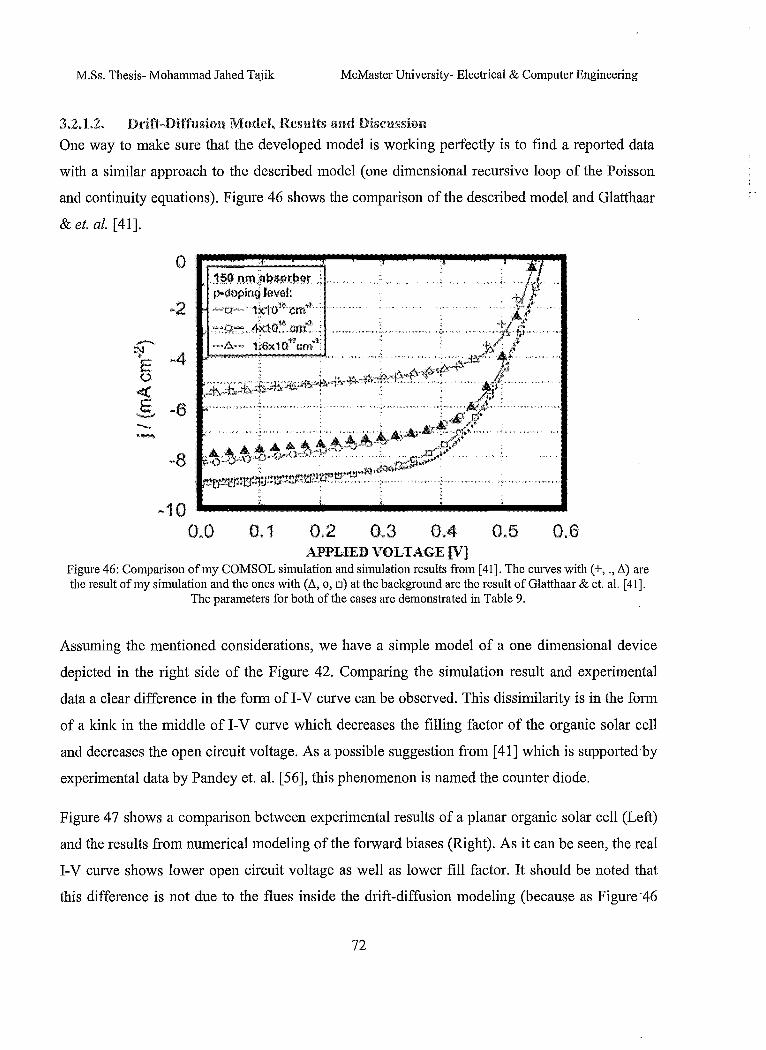
M.Ss. Thesis- Mohammad Jahed Tajik McMaster University- Electrical & Computer Engineering
3.2.1.2. Drift-HiffusionModel.Results and Discussion
One way to make sure that the developed model is working perfectly is to find a reported data
with a similar approach to the described model (one dimensional recursive loop of the Poisson
and continuity equations). Figure 46 shows the comparison of the described model and Glatthaar
& et. al. [41].
,......."
~ E ()
« E -~
-.... «~
o
-2
.. 4
-6
.. 10 0 .. 0 0.1 0.2 0.3 0.4 0.5 0.6
APPLIED VOLTAGE [V] Figure 46: Comparison of my COMSOL simulation and simulation results from [41]. The curves with (+, .,11) are the result of my simulation and the ones with (11, 0, D) at the background are the result of Glatthaar & et. al. [41].
The parameters for both of the cases are demonstrated in Table 9.
Assuming the mentioned considerations, we have a simple model of a one dimensional device
depicted in the right side of the Figure 42. Comparing the simulation result and experimental
data a clear difference in the form ofI-V curve can be observed. This dissimilarity is in the form
of a kink in the middle of I-V curve which decreases the filling factor of the organic solar cell
and decreases the open circuit voltage. As a possible suggestion from [41] which is supported-by
experimental data by Pandey et. al. [56], this phenomenon is named the counter diode.
Figure 47 shows a comparison between experimental results of a planar organic solar cell (Left)
and the results from numerical modeling of the forward biases (Right). As it can be seen, the real
I-V curve shows lower open circuit voltage as well as lower fill factor. It should be noted that
this difference is not due to the flues inside the drift-diffusion modeling (because as Figure '46
72
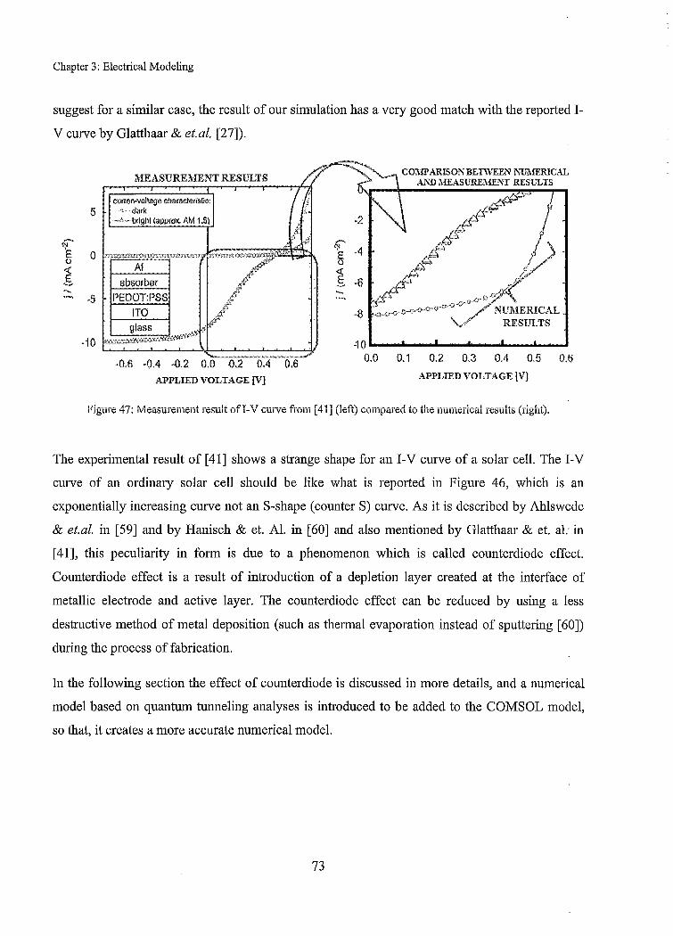
Chapter 3: Electrical Modeling
suggest for a similar case, the result of our simulation has a very good match with the reported I
V curve by Glatthaar & et.al. [27]).
MEASUREMENT RESuLTS
cumm'volfage ChOcact8listio: 5-"""dofK
-z, -- bright (appcox. AM 1.5j
-0,6 -0.4 -0,2 0,00.20,4 0:6 APPLIED VOLTAGE [V]
,.-..
" E 0 « E --
·4
·6
·8
COMP ARISON BETWEEN l\lJl\IERlCAL Al,,'D l\IEASUREl\ffi'\"T RESLLTS
40~--~--~--~--~--~--0.0 0.1 0.2 0.3 0.4 0.5 0.6
APPLIED VOLTAGE [\'1
Figure 47: Measurelllent result ofI-V curve fiOlll [41] (left) cOlllpared to the numerical results (right).
The experimental result of [41] shows a strange shape for an I-V curve of a solar cell. The I-V
curve of an ordinary solar cell should be like what is reported in Figure 46, which is an
exponentially increasing curve not an S-shape (counter S) curve. As it is described by Ahlswede
& et.al. in [59] and by Hanisch & et. AI. in [60] and also mentioned by Glatthaar & et. al: in
[41], this peculiarity in form is due to a phenomenon which is called counterdiode effect.
Counterdiode effect is a result of introduction of a depletion layer created at the interface of
metallic electrode and active layer. The counterdiode effect can be reduced by using a less
destructive method of metal deposition (such as thermal evaporation instead of sputtering [60])
during the process of fabrication.
In the following section the effect of counterdiode is discussed in more details, and a numerical
model based on quantum tunneling analyses is introduced to be added to the COMSOL model,
so that, it creates a more accurate numerical model.
73

M.Ss. Thesis- Mohammad Jahed Tajik McMaster University- Electrical & Computer Engineering
3.3. THE CORRECTION OF 'EI.ECTIUCAt MODEl, USH\fG TUNNEUNG CURRENT
In this section, it is tried to find a proper explanation for the difference between experimental and
numerical results. The I-V curve of a diode and ordinary solar cells and their equivalent circuits
are shown in Figure 48. Also Figure 49 shows how an I-V curve similar to the experimental
result (shown in Figure 47), can be made by adding the current of an ideal solar cell to the output
current of a shunt diode.
1-$
-f)t-I
~ Diode
V
~I
:7v -Solar cell
:0-I
Current I I I source
V
1-
Figure 48 : I-V curve of a diode, a current source and their parallel combination that makes a solar cell.
I-I
) Schottky Diode
»>m~_.
V
~ -f>.f csc
/. ?
Solar cell / V
~I Ideal solar cell
~~ •..•..••.••••••. ~ -Figure 49: The result of an ordinary solar cell and a parallel diode which will result into a I-V curve of a device similar to a
BH-OSC by including the effect of tunneling current (the counterdiode effect).
74

Chapter 3: Electrical Modeling
The term "counterdiode" was originally used for light emitting diodes (LEDs) that were used in
high frequency (which are mostly used in fiber optics). In this case, to increase the frequency of
the optical pulse generated by LED or simply shrinking the width of the pulses, the Zener diode
would be used to discharge the inside capacitance of LED to make it ready for the next pulse. In
the case of no counterdiode, this capacitance will be discharged through the leakage that will
take a long time [61].
In the case of organic solar cells, the counterdiode phenomenon is also due to a shunt diode
which is connected in parallel to the solar cell, with the following major differences:
Despite the name, as can be seen in the schematic model that is shown in Figure 49, the
shunt diode has the same direction of the solar cell's diode.
Unlike the LED circuit, in the case of BH-OSC, there is actually no real shunt diode
connected in parallel with the device and this is just the equivalent model.
Here, physical phenomenon behind this "counterdiode" effect must be described. Prior to this
description, we should take a closer look at the junction of the metallic electrode and active
layer. While the metallic electrode is getting deposited on top of the organic blend (in our case
Aluminum), because of the high rate of activity in freshly deposited aluminum atoms, the weak
Vanderwall's bound between the first couple of layers of organic material, will break and this
will results in surface states in the middle of the active layer's bandgap [31,64].
On the other hand, in an organic-metal junction the first couple of molecular layers at the
interface lose their charges, just like a conventional semiconductor-metal junction. For the
conventional junction those charges will be replaced by the charges nearby, because of the
electrical connection in the semiconductor's lattice. However, in organic material, apart from
very high or very low energies, most of the energy states are local. Therefore, if they get depleted
by the metallic electrode at the junction, there will be no flow of nearby charges to replace them.
This will result in a very thin layer that has a wider bandgap, similar to an insulator. Thus,. as
shown in Figure 50, the band diagram of an organic solar cell should be modified by adding an
insulator layer at the junction [66].
75
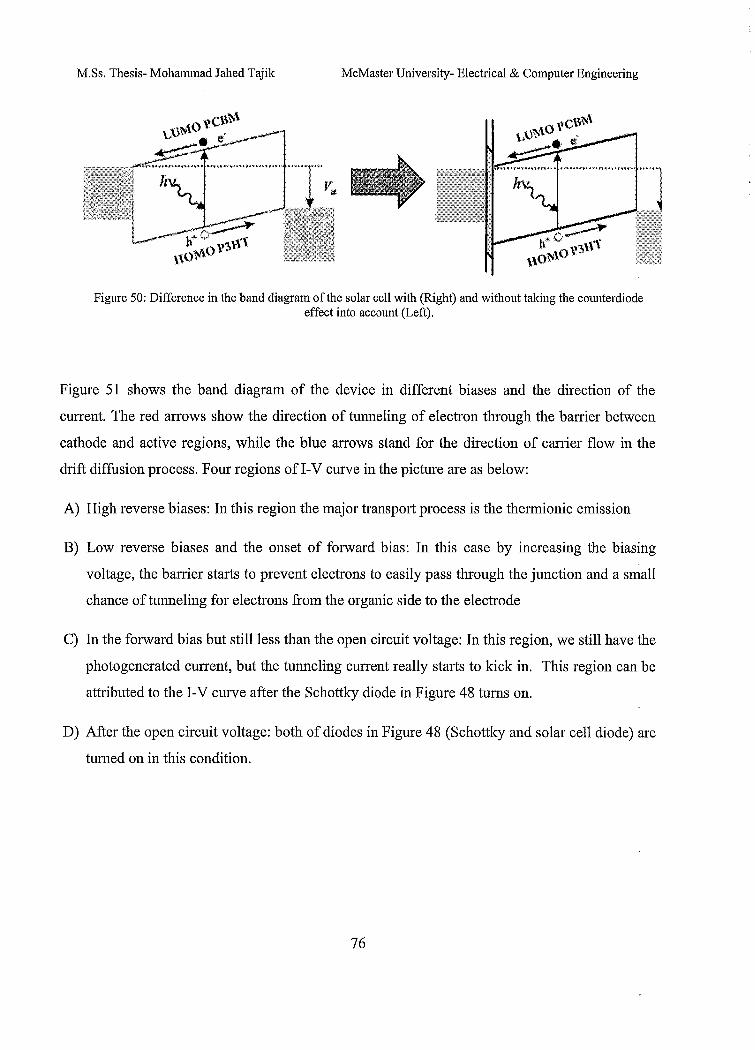
M.Ss. Thesis- Mohammad Jahed Tajik McMaster University- Electrical & Computer Engineering
Figure 50: Difference in the band diagram of the solar cell with (Right) and without taking the counterdiode effect into account (Left).
Figure 51 shows the band diagram of the device in different biases and the direction of the
current. The red arrows show the direction of tunneling of electron through the barrier between
cathode and active regions, while the blue arrows stand for the direction of carrier flow in the
drift diffusion process. Four regions ofI-V curve in the picture are as below:
A) High reverse biases: In this region the major transport process is the thennionic emission
B) Low reverse biases and the onset of forward bias: In this case by increasing the biasing
voltage, the barrier starts to prevent electrons to easily pass through the junction and a small
chance of tunneling for electrons from the organic side to the electrode
C) In the forward bias but still less than the open circuit voltage: In this region, we still have the
photogenerated current, but the tunneling current really starts to kick in. This region can be
attributed to the I-V curve after the Schottky diode in Figure 48 turns on.
D) After the open circuit voltage: both of diodes in Figure 48 (Schottky and solar cell diode) are
turned on in this condition.
76

Chapter 3: Electrical Modeling
D)
<)I
E tl 1 0 1"""':i,~",'m,"dd:f'fD"'''tift')'rln4a,'
A ·5
D
·0.6 -0.4 -0.2 0.0 0.2 0.4 0.6 V/V
Figure 51: Band diagram of a solar cell for different biasing and the direction of the current. Blue arrows stand for the direction of the carrier due to the thermionic emission and the red arrows show the direction of electron tunneling the barrier at the interface (at the left). The experimental result from [41] with separated region in the
bias for each one of the four conditions at the left.
Consequently, the total current can be divided into the following sections:
1- Thermionic emission current
2- Tunneling from the organic layer to the metallic contact
3- Tunneling from the metallic contact to the organic layer
The first part was calculated in the previous section. The second current is mostly in the reverse
biases that are important for us. The most important parameters for organic solar cells' fill factor
(fill factor or FF is the ratio of maximum generated power to product of short-circuit current and
open circuit voltage) and efficiency, can be calculated by the information that is provided in the
region C of Figure 51, which is the same region that the third current exists.
The current density passes through a thin barrier can be calculated by the following equation
[66]:
Equation 60
In this equation, q stands for electron charge, p is the distribution of charges, f is the Fermi's
function, px is the momentum of electron in the direction of x and T is the transport coefficient.
77
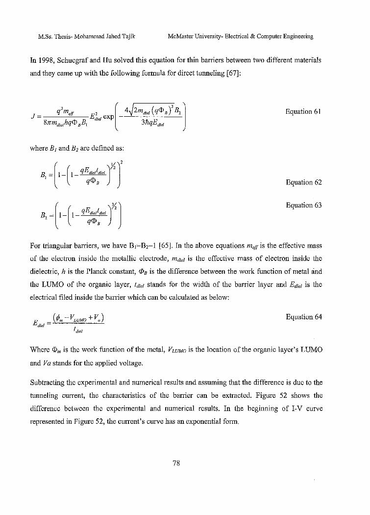
M.Ss. Thesis- Mohammad Jahed Tajik McMaster University- Electrical & Computer Engineering
In 1998, Schuegraf and Hu solved this equation for thin barriers between two different materials
and they came up with the following formula for direct tunneling [67]:
Equation 61
whereB1 andB2 are defined as:
Equation 62
Equation 63
For triangular barriers, we have B1=B2=1 [65]. In the above equations mejJis the effective mass
of the electron inside the metallic electrode, mdiel is the effective mass of electron inside the
dielectric, h is the Planck constant, qJB is the difference between the work function of metal and
the LUMO of the organic layer, tdiel stands for the width of the barrier layer and Ediel is the
electrical filed inside the barrier which can be calculated as below:
E _ (rpm - VWMO + Va) diel - t
diel
Equation 64
Where <Pm is the work function of the metal, VWMO is the location of the organic layer's LUMO
and Va stands for the applied voltage.
Subtracting the experimental and numerical results and assuming that the difference is due to the
tunneling current, the characteristics of the barrier can be extracted. Figure 52 shows the
difference between the experimental and numerical results. In the beginning of I-V curve
represented in Figure 52, the current's curve has an exponential form.
78

Chapter 3: Electrical Modeling
Dirf e .. en ce b ehv eeUll nm elienl Ull (Jm enfllu'em fll t re~lllts Fr---'---~----~--'----r--~----
().Os (1,1 0,15 0,2 0,25 Q,3 (1,35 (1.4 !MS
Voltage IV]
Figure 52: The difference between the experimental I-V curve and numerical result that are shown in Figure 47
Based on the above, the ttlIh'leling current formula as a ftlnction of applied voltage on Al
becomes as below:
Jtullneling == Equation 65
J'"l1l1elillg (0,3) for X < V
To find the best fit with the curve in Figure 52, two parameters can be used:
The barrier height
The barrier width
By changing the barrier's width, the resistance of the interface layer changes which leads to
changes in slope of the I-V curve (by increasing the thickness I-V curve becomes more
nonlinear), By increasing/decreasing the barrier's height, the magnitude of the current,
dramatically decreases/increases, Figure 53, shows the curves of the modified tunneling current
for three different barrier thicknesses (10nrn, 7nrn and 3nrn) with forty different heights of the
barrier distributed from 1 e V to 2e V.
79

M.Ss. Thesis- Mohammad Jahed Tajik McMaster University- Electrical & Computer Engineering
18000
1600a
"'E 12000 ,Q :[ 10000
C 8000
~ 8 6000
16
0.7
OJ,
0,5
0.1
TllnMllng current [mA.cnf21 for a 311t1llhlckbarrier
r/ [jJr"(tiOI1('fln<rea~lng. ../ / th.l,.rrl~"'<helght ~
/' ./'~---
/~.~""-
"'. ,,~~ ... -
Tunneling cu",mt [IllNCIll3J lor a 5nm thick harrier
0.00
Direction of inct~at;r"g the barr;"r's height
0.1 0 IS 0;2 0.25 Applied voltage M
0.3
i'unnullng current IrnA-em']') for a 1nm thick barriar
Direction "fi",roM,lug the barri.r'.s h~ight
0.35
°O~~~O~.05~~=O~.1~~~~==~==~~~~----~O.~5 . . 0.15 0.2 0.25 0.3 •
Applied voltage M Figure 53: Modified tunneling cunent for three different banier widths (3nm, 7nm and 10nm) with forty different banier heights from 1 e V to 2e V. The direction of the red anows in the pictures indicates the increase in the banier
height
80

Chapter 3: Electrical Modeling
Finally by comparing different results of the modified tunneling current, the best match can be
found with the parameters that are shown in Table 10. Figure 54 shows comparison between the
experimental and the best matches in the first and the second (modified) tunneling current model.
o ~1
_ ·2 N
l=> ~ ~3 ~
== 4 e ~ -5 I.. :l
NU;\lERICAL + TUNNELING-CORRECTION
U.6 R
Our numerical model result
MeaSlll'ement result
.7
0.1 o.z f},3 0.4 0.5 1),6
Voltage [V] Figure 54: Comparison of calculated I-V corrected by tunneling current (circles) with measurement results reported
by Glatthaar et. al. [41] (triangles).
As Figure 54 shows, the comparison of numerical result (which is modified by the tunneling
current correction) have a good agreement with the experimental result.
T bl 10 P a e h arameters t at are use III 1 ure 54
Parameter's symbol Parameter's quantity Equation men/mdiel 1.6 Equation 65
<PB 1.8geV Equation 65 {diel 5.56nm Equation 64
After finding the proper fit for the tunneling current, the question come into mind that "how
should the two of the current be combined to produce the final result? ". By taking a look at
Figure 51, it becomes clear that tunneling current is injecting electrons into the active region (in
section C and D) or taking out electrons from the active region (in section B). Therefore,
tunneling current acts as the generation or recombination in Equation 50 and Equation 51 and we
can rewrite them as:
81
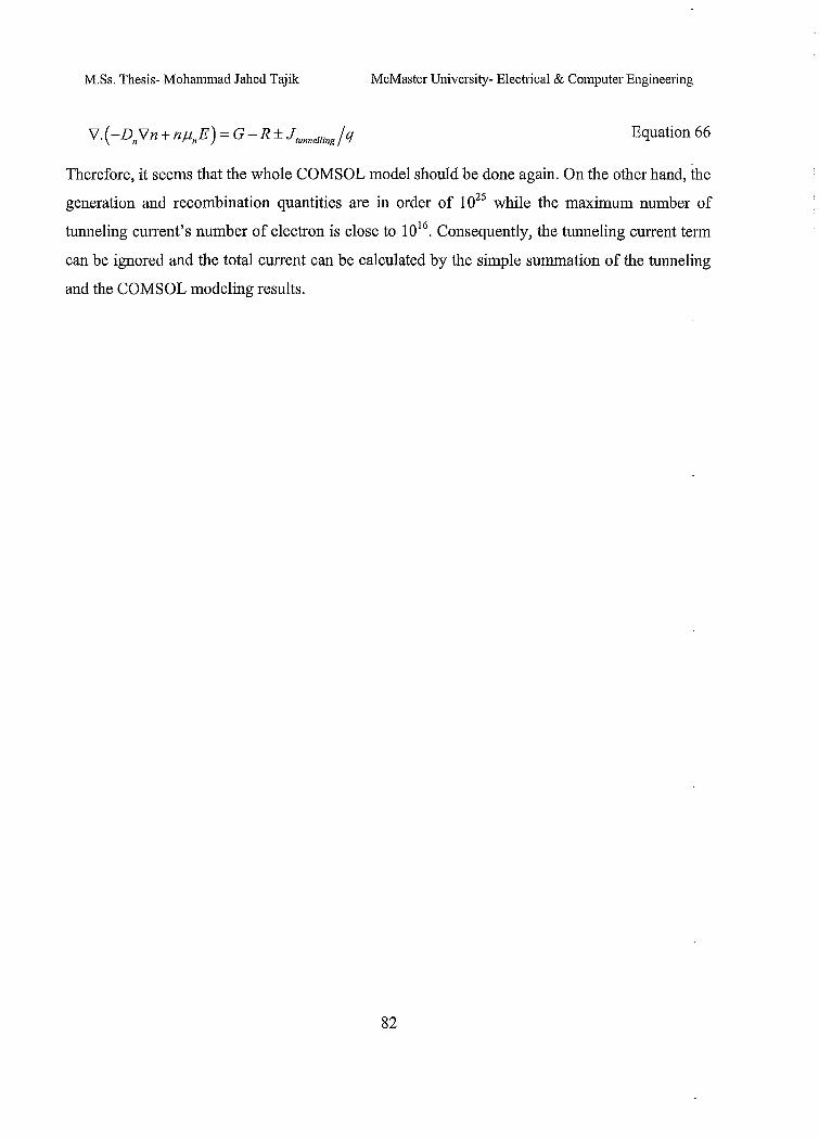
M.Ss. Thesis- Mohammad Jahed Tajik McMaster University- Electrical & Computer Engineering
\/.( -Dn \/n +nJinE) = G-R ± J'"nnelling/q Equation 66
Therefore, it seems that the whole COMSOL model should be done again. On the other hand, the
generation and recombination quantities are in order of 1025 while the maximum number of
tunneling current's number of electron is close to 1016. Consequently, the tunneling current term
can be ignored and the total current can be calculated by the simple summation of the tunneling
and the COMSOL modeling results.
82

Chapter 4: Conclusion and Suggestion
CHAPTER 4
CONCLUSION AND RECOMMENDATION
4. CONCLUSION AND RECOMMENDATION FOR FUTURE WORK
4.1. CONCLUSION
In this thesis, the mechanism of conversion of optical power to electrical power for two types of
organic solar cells (bilayer and bulk heterojunction solar cells) was studied.
In order to model organic solar cells, the thesis was divided into two separate sections:
Optical section (Chapter 2)
Electrical section (Chapter 3)
In the optical section, the following mechanisms were studied:
In-coupling of the photons
Absorption of the photons
Formation of the excitons
In Chapter 2, it was discussed that COMSOL software can be successfully used to model the
propagation of light inside an organic solar cell. Also, it was shown that by adding an extra layer
focusing apertures at the top of planar bilayer heterojunction organic solar cells, the absorption
of light around the active layers' junction, which is a vital area for power conversion inside such
solar cells, can be increased up to 98%.
In the next section of the thesis, the electrical performance of the organic solar cell for the
following mechanisms was studied:
Diffusion of the excitons
83

M.Ss. Thesis- Mohammad Jahed Tajik McMaster University- Electrical & Computer Engineering
Dissociation of the excitons into electrons and holes and the transportation of the charges
Collection of the charges at the electrodes
By a comparison between experimental and electrical model results, it was concluded that a
simple drift diffusion model that only considers the thermionic emission mechanism as the only
component of generated photo current in a bulk heterojunction organic solar cell is not sufficient
by itself. Thus there is a need for a new model to include the effect of charge injection at the
electrodes' interfaces. Therefore, a tunneling current correction was introduced. By fmding the
best fit using trial and error, connection of organic material and metallic electrode was
characterised.
It should be noted that the mentioned tunneling current or the so called "counterdiode effect" in
the field of organic devices had been studied only for organic LEDs in the literature and by
modeling the counterdiode effect via tunneling current model for the organic solar cells the last
section can be attributed as a contribution to the literature.
It2. RECOMMENDATION
For the future work, on the optical modeling of organic solar cells, two different approaches are
suggested:
Modeling new applications using the presented models
Developing new models based on the present work
In the case of new applications, new types of focusing deformities or new designs of organic
solar cells (for instance, changing the order of the layers or adding new layers with new types of
organic or inorganic materials) can be proposed. Another interesting structure is an organic solar
cell with two metallic electrodes, where one of the sides has some holes in it to allowing the
sunlight into the device and to be trapped there. To increase the intensity of light inside of the
solar cell, some focusing deformities at the top layer can be used.
84

Chapter 4: Conclusion and Suggestion
Also, studying the effect of a photonic crystal at the first layer of organic solar cells to increase
the absorption and reduce the back reflection of light by the existing three dimensional optical
model is possible.
For developing new models, upgrading the one dimensional analytical model into two and three
dimensional models or creating a new numerical model for bulk heterojunction organic solar
cells based on the existing numerical models, this time by including a detailed model, whIch
consist of nanometeric islands of one type of organic material inside another type of organic
material, is strongly suggested.
Similar to the optical recommendations, for the future electrical models suggestions can be
divided into the two following group:
Modeling new applications using the present models
Deveioping new models based on the present work
For the first category (new applications), new types of planar organic solar cells such as folded
structure or multistage planar organic solar cells can be modeled using the proposed electrical
model. These types of organic solar cells have a better efficiency, because of their better light
absorption ability, but because of their multilayer design the electrical properties of them is
deteriorated. Therefore, modeling can be helpful for improving the electrical design to get even
better performances for these multilayer OSCs.
For the second category, new methods of transport modeling for organic materials can be
developed. These methods may include more complicated quantum mechanical analyses. For
example, ab initio methods and the Hartree-Fock method for a very accurate molecular model
and true modeling the orbital distribution of electron. These accurate methods can be used for the
prediction of molecular scale (some nano meter) phenomena such as connections and interfaces.
However, because of high computational cost to model larger devices, it is better to use other
quantum mechanical analyses such as density functional theory (DFT), which is a good quantum
mechanical method for devices around the ranges of planar organic solar cells (a few lOOnm).
DFT analysis is usually compound with Non-equilibrium Green's function (NEGF) method,
which is a good computational approach to solve the Schrodinger's equation for similar devices.
85
M.Ss. Thesis- Mohammad Jahed Tajik McMaster University- Electrical and computer engineering
REFERENCES
1- A. J. Waldau, "PV Status Report 2003", European Commission, EUR 20850 EN, 2003.
2- "Report on new trends in Solar cells", The U.S. National Renewable Energy Laboratory (NREL), 2010, Available: http://www.mel.gov/.
3- Annual report, "Next-Generation Organic Solar Cell Technology and Market Forecast", Displaybank Co. Ltd, Feb 2010.
4- L. Kazmerski, "NREL compilation of best research solar cell efficiencies ", National Renewable Energy Laboratory, National Renewable Energy Laboratory (NREL), 2010.
5- F. C. Krebs, "Fabrication and processing of polymer solar cells: A review of printing and coating techniques", Solar Energy Materials & Solar Cells, Vol. 93, pp. 394-412,2009.
6- M. Haeussler, "Fabrication of organic photovoltaic devices", article in "A to Z of nanotechnology", Oct 25, 2009.
7- E. Becquerel and L. Lumiere: "Ses causes et ses effets", tome second, Paris, pp. 122. 1867.
8- H. Hertz, "Uber eine Anfluss des ultravioletten Lichtes auf die electrische Entladung", Annalen der Physik und Chemie, Vol. 31, pp. 983-1000, 1887.
9- "The Nobel Prize in Physics 1921 ", Nobelprize.org, 26 Sep. 2010, Available: http://nobelprize.org/nobel prizes/physics/laureatesl192l1index.html.
10- J. Perlin, "From space to earth: the story of solar electricity", Harvard University Press: Cambridge, MA, 2002.
11- P.M. Borsenberger and D.S. Weiss, "Organic photoreceptors for imaging systems ", Marcel Dekker, New York, 1993.
12- C. K. Chiang, C. R. Fincher, Y.W. Park, A. J. Heeger, H. Shirakawa, E. J. Louis, S. C. Gau and A. G . . MacDiarmid, "Electrical conductivity in dopedpolyacetylene", Physical Review Letters, Vol. 39, pp. 1098-1101, 1977.
13- H. Shirakawa, A. G. MacDiarmid and A. J. Heeger, "Twenty-five years of conducting polymers ", Chemical Communications, Vol. 1, pp. 1,2003.
14- C. W. Tang, "Two-layer organic photovoltaic cell", Applied Physics Letters, Vol. 48, pp. 183-185, 1986.
15- J. Li, "Solarmer energy, Inc. breaks psychological barrier with 8.13% OPV efficiency", Solarmer Energy, Inc. 27 June 2010, Available: http://www.forbes.comlfeeds/businesswire/201 0107127 /businesswire142993163 .html.
16- S. S. Sun and N. Serdar Sariciftci, "Organic Photovoltaics ", Taylor & Francis Group LLC. 2005.
17- T. Kietzke, "Recent advances in organic solar cells", Advances in OptoElectronics, Review Article, Hindawi Publishing Corporation, Vol. 2007, pp. 15,2007.
18- T. L. Benanti, D. Venkataraman, "Probing the chiroptical response of a single molecule: fluorescence detected circular dichroism from individual helicene molecules ", Photosynthesis Research, 87, pp. 73-81, 2006.
19- H. Hoppea and N. S. Sariciftci, "Organic solar cells: An overview", Journal of Materials Research, Vol. 19, pp. 7,2004.
86

M.Ss. Thesis- Mohammad Jahed Tajik McMaster University- Electrical and computer engineering
20- D. P. Grubera, G. Meinhardtb and W. Papousekc, "Modelling the light absorption in organic photovoltaic devices", Solar Energy Materials and Solar Cells, Vol. 87, pp. 215-223, 2005.
21- A. K. Ghosh and T. Feng, "Merocyanine organic solar cells", Journal of Applied Physics, Vol. 49, pp. 5982, 1978.
22- J. Wagner, T. Fritz, and H. Bottcher, "Computer modelling of organic thin film solar cells. 1. exciton model of photocurrent generation", Physica Status Solidi A, Vol. 136, pp. 423,1993.
23- A. De'sormeaux, J. J. Max, and R. M. Leblanc, "Photovoltaic and electrical properties of aluminum/LangmuirBlodgett films/silver sandwich cells incorporating either chlorophyll a, chlorophyll b, or zinc porphyrin derivative", Journal of Physical Chemistry, Vol. 97, pp. 6670, 1993.
24- C. W. Tang and A. C. Albrecht, "Photovoltaic effects ofmetal-chlorophyll-a-metal sandwich cells", Journal of Chemical Physics, Vol. 62, pp. 2139, 1975.
25- A. K. Ghosh, D. L. Morel, T. Feng, R. F. Shaw, and C. A. Rowe, Jr., "Photo voltaic and rectification properties of AVMgphthalocyanineiAg Schottky-barrier cells", Journal of Applied Physics, Vol. 45, pp. 230,1974.
26- H. B. DeVore, "Spectral distribution ofphotoconductivity", Physical Review, Vol. 102, pp.86, 1956.
27- L. G. Yang, H. Z. Chen and M. Wang, "Improved method of determining exciton diffusion length from thickness-dependent photocurrent response of organic heterojunction ", Thin Solid Films, Vol. 516, pp. 7701-7707, 2008.
28- L. A. A. Pettersson, Lucimara S. Roman, and Olle Inganas, "Modeling photocurrent action spectra of photovoltaic devices based on organic thin films ", Journal of Applied Physics, Vol. 86, pp. 487, 1999.
29- G. Z. Ran, W. Q. Zhao, G. L. Ma, L. Dai and G. G. Qin, "Role of the dielectric capping layer in enhancement of light outcoupling for semitransparent metal-cathode organic light-emitting devices ", Journal of Optics A: Pure and Applied Optics, Vol. 8, pp. 733-736,2006.
30- M. Niggemann, M. Riede, A. Gombert, and K. Leo, "Light trapping in organic solar cells", Wiley-VCH -physica status solidi (a), Vol. 205, pp. 2862-2874, 2008.
31- N. K. Persson, M. S. and O. Inganias, "Anomalous behaviour of the photoacoustic signal near the phase transition in the thallium blue bronze(T1O.3Mo03)", Solar Energy Materials & Solar Cells, Vol. 83, pp. 169-186, 2004.
32- R. J. Matson, K. A. Emery and R. E. Brid, "Solar Cells, Terrestrial solar spectra, solar simulation and solar cell short-circuit current calibration: A review", Solar Cells, Vol. 11, pp. 105-145, 1984.
33- COMCOL Inc. Available: http://www.comsol.coml.
34- M. Abkowitz et.al. "Springer Handbook of electronic and photonic materials ", Springer, 2006.
35- Z.T. Liu, C.Y. Kwong, C.H. Cheung and A.B. Djurisi, "The characterization of the optical jitnctions of BCP and CBP thinfilms by spectroscopic ellipsometry", Synthetic Metals, Vol. 150, pp. 159-163,2005.
36- "Isotropic organic semiconductor for OPVs and OLEDs", Aldrich Chemical Co., Inc. Sigma-Aldrich Corporation, "Your Materials Matter." Data sheet, 2008.
37- J. D. Lindberg, R. E. Douglass and D. M. Garvey, "Carbon and the optical properties of atmospheric dust", Journal of Applied Optics, Vol. 32, pp. 21, 1993.
38- S. Laux, N. Kaiser, A. ZoEller, R. GoEtzelmann, H. Lauth and H. Bernitzki, "Room-temperature deposition of indium tin oxide thin films with plasma ion-assisted evaporation ", Thin Solid Films Vol. 335, pp.l-5, 1998.
87
M.Ss. Thesis- Mohammad Jahed Tajik McMaster University- Electrical and computer engineering
39- R. Kashyap, "Theory offiber bragg gratings", Academic Press, London, 1999.
40- R. Loudon, "The quantum theory oflight", Oxford U. Press, Oxford, 1994.
41- M. Glatthaar, M. Riede, N. Keegan, K. Sylvester-Hvid, B. Zimmermann, M. Niggemann, A. Hinsch and A. Gombert, "ITO-free wrap through organic solar cells-a module concept for cost-efficient reel-to-reel production ", Solar Energy Materials and Solar Cells, Vol. 91, pp. 390-393,2007.
42- A. Kahn, W. Zhao, W. Gao, H. Va'zquez and F. Flores, "Doping-induced realignment of molecular levels at organic-organic heterojunctions", Chemical Physics, Vol. 325, pp. 129-137,2006.
43- V. Dyakonov, "Mechanisms controlling the efficiency of polymer solar cells", Applied Physics A, Vol. 79, pp. 21,2004.
44- L. J. A. Koster, E. C. P. Smits, V. D. Mihailetchi, and P. W. M. Blom, "Device model for the operation of polymerlJullerene bulk heterojunction solar cells", Physical Review B, Vol. 72, pp. 085205,2005.
45- J. C. C. Fan, F. J. Bachner and G. H. Foley, "Effect of 02 pressure during deposition on properties of if-sputtered Sn -doped In203 films ", Applied Physics Letters, Vol. 31, pp. 773-775, 1977.
46- K. Sreenivas, T. Sundarsen Rao, A. Mansnigh and S. Chandr, "Preparation and characterization of r j sputtered indium Tin oxidefilms", Journal of Applied Physics, Vol. 57, pp. 384-392,1985.
47- J. Szczyrbowski, A. Dietrich and H. Hoffmann, "Optical and electrical properties of r j sputtered indium-tin oxidefilms", Physica Status Solidi A, Vol. 78, pp. 243-252,1983.
48- M. Buchanan, J. B. Webb and D. F. Williams, Thin Solid Films, "The influence of target oxidation and growth related effects on the electrical properties of reactively sputteredfilms of tin-doped indium oxide", Thin Solid Films, Vol. 80, pp. 373-382, 1981.
49- M. Higuchi, S. Uekusa, R. Nakano and K. Yokogawa, "Post-deposition annealing influence on sputtered indium tin oxide film characteristics", Japanese Journal of Applied Physics, Vol. 33, pp. 302-306, 1994.
50- N. Balasubramanian and A. Subrahmanyam, "Effect of substrate temperature on the electrical and optical properties of reactively evaporated indium tin oxide films ", Materials Science and Engineering, B 1 pp. 279-281, 1988.
51- J. Bregman, Y. Shapira and H. Aharoni, "Effects of oxygen partial pressure during deposition on the properties of ion-be am-sputtered indium-tin oxide thinfilms", Journal of Applied Physics, Vol. 67, pp. 3750-3753, 1990. -
52-H. Haitjema and J. J. Ph. Elich, "Physical properties of pyrolitically sprayed tin-doped indium oxide coatings ", Thin Solid Films, Vol. 205, pp. 93-100, 1991.
53- C. C. Yap, M. Yahaya and M. M. Salleh, "Irifluence oftetrabutylammonium hexafluorophosphate (TBAPF6) doping level on the peiformance of organic light emitting diodes based on PVK: PBD blend films ", Current Applied Physics, Vol. 9, pp. 722-726, 2009.
54- A. K. Narula, R. Singh, K. L. Yadav and K. B. Ravat, Subhas Chandra, "Effect of synthesis temperature and doping level on conductivity and structure of poly(3-methyl thiophene) ", Applied Biochemistry and Biotechnology, Vol. 96, pp. 109-II7, 200l.
55- M. Glatthaar, N. Mingirulli, B. Zimmermann, T. Ziegler, R. Kern, M. Niggemann, A. Hinsch and A. Gombert, "Impedance spectroscopy on organic bulk-heterojunction solar cells", Hysica Status Solidi (A) Applications and Materials, pp. 202-125,2005.
56- A. K. Pandey, J. M. Nunzi, H. Wang, C. C. Oey, A.B. Djurisic, M. H. Xie, Y. H. Leung, K. K. Y. Man and W. K. Chan, "ReverseBiased Annealing: Effective post treatment tool for polymerlnano-compositesolar cells ", Organic Electronics 8, pp. 396---400,2007.
88
M.Ss. Thesis- Mohammad Jahed Tajik McMaster University- Electrical and computer engineering
57- "COMSOL Multiphysics Modeling Guide (COMSOL 3.5a)", COMSOL AB, Burlington MA USA, November 2008.
58- "Reference Guide (COMSOL 3.5a)", COMSOL AB, Burlington, MA USA, November 2008.
59- E. Ahlswede, J. Hanisch, and M. Powalla, "Influence of cathode sputter deposition on organic solar cells", Applied Physics Letters, Vol. 90, No. 063513,2007.
60- J. Hanisch, E. Ahlswede, M. Powalla, "All-sputtered contacts for organic solar cells", Thin Solid Films Vol. 5l6,pp.724l-7244,2008.
61- C. J. Schneider, N. Engelberts and J. D. P. van Dijk, "Characteristics of a passive RF field probe with fibreoptic link for measurements in liquid hyperthermia phantoms ", Physics in Medicine and Biology, Vol. 36, pp. 46-474, 1991.
62- M. Martin, J.-J. Andre, and J. Simon, "Influence of dioxygen on the junction properties of metallophthalocyanine based devices", Journal of Applied Physics, Vol. 54, pp. 2792, 1983.
63- M. Whalley, "Absorption spectra of tetrazaporphins and phthalocyanines. Formation of pyridine salts ", Conjugated macro cycles. Part XXXII. Journal of the Chemical Society, Vol. 1, pp. 866-869, 1961.
64- R. Koeppe and N. Serdar Sariciftci, "Complexation of pyrrolidinofullerenes and zinc-phthalocyanine in a bilayer organic solar cell structure", Applied Physics Letters, Vol. 87, No. 244102, 2005.
65- A. Gehring and S. Selberherr, "Modeling of tunneling current and gate dielectric reliability for nonvolatile memory devices ", IEEE Trans. On Device & Materials Reliability, Vol. 4, Issue 3, 2004.
66- S. M. Sze, "Physics of Semiconductor Devices", 2nd Edition, John Wiley & Sons, Inc. 1981.
67- K. F. Schuegraf, C. C. King, and C. Hu, "Ultrathin silicon dioxide leakage current and scaling limit", Symp. VLSI Technol. Tech. Dig., pp. 18-19, 1992.
68- A. B. Walker, A. Kambili and S. J. Martin, "Modelling temperature-dependent current voltage characteristics of an MEH-PPVorganic light emitting device", Journal of Physics: Condensed Matter, Vol. 14, pp. 9825-9876, 2002.
89