angular resolved light scattering of structured tcos for ... · iccg 8 - braunschweig 2010 -...
TRANSCRIPT

ICCG 8 - Braunschweig 2010 - Proceedings 415
Session 7 - Solar Applications
sess
ion
7 -
7.0
4
angular resolved light scattering of structured tcos for the appli-cation in a-si:h/µc-si:h solar cellsW. Dewald1, V. Sittinger1, B. Szyszka1, A.Gordijn2, J. Hüpkes2, F. Hamelmann3, H. Stiebig3, F. Säuberlich4
1 Fraunhofer Institute for Surface Engineering and Thin Films IST,
Braunschweig, Germany
2 Institut für Energieforschung 5 - Photovoltaik, Forschungszen-
trum Jülich, Jülich, Germany
3 Malibu GmbH & Co. KG, Bielefeld, Germany
4 Sunfilm AG, Bitterfeld-Wolfen, Germany
�Keywords:� zinc wxirK, light toapping, thin film dilicwn tanrKm dwlao cKll, angulao oKdwlvKr dcattKo-ing, toandpaoKnt cwnructivK wxirK
1 Introduction
In thin film micromorph solar cells (a-Si:H/µc-Si:H) an effective light trapping is crucial for a good performance. Up to now different approaches have been developed reaching from CVD deposition of rough TCOs like SnO2:F over LPCVD ZnO:B to the post deposition etching of magnetron sputtered ZnO:Al. Here the sputter technique is essential for the obtained etch morphology, e.g. reactive MF magnetron sputtering, RF or DC excitation.
Usually rough transparent surfaces are characterized by their haze, which is a scalar value and is directly connected to the rms-roughness. The haze value is not sufficient to determine or predict the enhance-ment of short circuit currents due to light trapping of varying structures [1], but this would be necessary for industrial production lines. An approach to overcome this is to focus on angular resolved light scattering (ARS). The lateral structure properties contain important information for light trapping purposes, which is gathered by angular light scatter-ing.
2 Experimental
The measurement is performed step by step in an in-plane geometry where the detector circles the sample. Hereby the angular distribution function (ADF) of the scattered light was obtained for the above mentioned TCOs, also known as angular resolved scattering (ARS). Details about the accessory can be found in [2].
The incident light hits the sample perpendicular and
is scattered as shown in Fig. 1. The detector circles the sample on the dotted line and cuts the light scattering cone with opening angle J only twice (one point is marked by the grey square in Fig. 1).
Fig. 1. PoinciplK wf angulao oKdwlvKr dcattKoing mKa-duoKmKntd in toandmittancK mwrK. ThK rKtKctwo (goKe dquaoK) mwvKd in-planK. ThK dignal had tw bK yKightKr be intKgoatiwn wvKo thK azimuthal anglK at cwndtant J.
Because the measuring is performed in in-plane geometry, the data was integrated over all azimuthal scattering angles to include the whole light scatter-ing cone at a certain polar angle J (see Fig. 1). This assumption is correct if the sample is isotropic, which leads to a symmetric ARS-signal as can be seen in Fig. 2.
3 Results
All analyzed samples in Fig. 2 were etched after deposition except of NSG and the LPCVD ZnO:B. Fluorine doped tin oxide (NSG) shows the least scattering, reactively sputtered ZnO:Al and ZnO:B deposited by LPCVD demonstrated varying scattering according to their structure sizes. The highest scattering is obtained by pure RF sputtering (For schungszentrum Jülich) or a new RF seed layer approach of the Fraunhofer IST (see poster presenta-tion 5.16).
Direct transmittance is set to zero degree scattering angle. The signal was integrated over the azimuthal angle at constant J and the finite size of the detec-tor was taken into account.
416 ICCG 8 - Braunschweig 2010 - Proceedings
Session 7 - Solar Applications
sess
ion
7 -
7.0
4
Fig. 2. Angulao oKdwlvKr dcattKoing mKaduoKmKntd wf riffKoKntle poKpaoKr rwpKr anr KtchKr ZnO damplKd wn gladd at 700 nm.
To gain further insight, not only a single wavelength was observed but a whole spectrum along every single angular step of the detector was collected for selected samples. This gave insight to the varying ADF shape at different wavelengths (compare Fig. 3). Scattering is strongest at short wavelengths and becomes less at long wavelengths. This behavior is known from haze values as well.
Fig. 3. Angulao oKdwlvKr dcattKoing wf thK KtchKr RF dputtKoKr damplK fowm FwodchungdzKntoum Jülich, mKaduoKr fwo thK yhwlK dpKctoum bKtyKKn 350 anr 800 nm.
Some post deposition etched samples tend to show an anisotropic etching. As expected here the light scattering is asymmetric. The data should not be integrated as usual, because structures and scatter-ing are anisotropic.
ZnO:B prepared by LPCVD exhibits varying pyramidal structures’ sizes according to deposition parameters and therefore a different scattering behavior. The
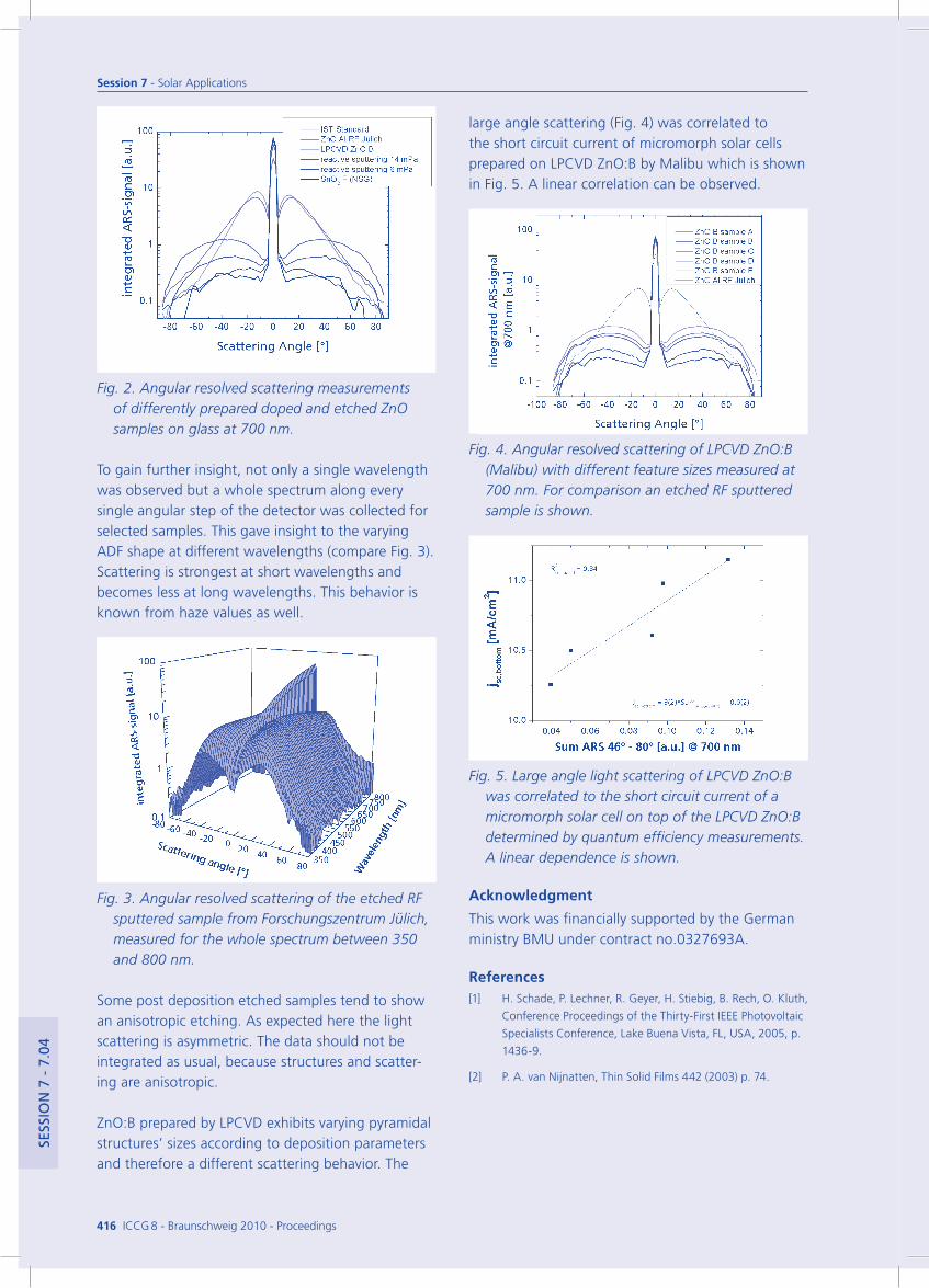
large angle scattering (Fig. 4) was correlated to the short circuit current of micromorph solar cells prepared on LPCVD ZnO:B by Malibu which is shown in Fig. 5. A linear correlation can be observed.
Fig. 4. Angulao oKdwlvKr dcattKoing wf LPCVD ZnOs:B (Malibu) yith riffKoKnt fKatuoK dizKd mKaduoKr at 700 nm. Fwo cwmpaoidwn an KtchKr RF dputtKoKr damplK id dhwyn.
Fig. 5. LaogK anglK light dcattKoing wf LPCVD ZnOs:B yad cwooKlatKr tw thK dhwot ciocuit cuooKnt wf a micowmwoph dwlao cKll wn twp wf thK LPCVD ZnOs:B rKtKominKr be quantum KfficiKnce mKaduoKmKntd. A linKao rKpKnrKncK id dhwyn.
Acknowledgment
This work was financially supported by the German ministry BMU under contract no.0327693A.
References[1] H. Schade, P. Lechner, R. Geyer, H. Stiebig, B. Rech, O. Kluth,
Conference Proceedings of the Thirty-First IEEE Photovoltaic
Specialists Conference, Lake Buena Vista, FL, USA, 2005, p.
1436-9.
[2] P. A. van Nijnatten, Thin Solid Films 442 (2003) p. 74.