anion exchange in ii vi semiconducting nanostructures via ... · explained through...
TRANSCRIPT
Anion Exchange in II−VI Semiconducting Nanostructures via AtomicTemplatingRahul Agarwal,† Nadia M. Krook,† Ming-Liang Ren,† Liang Z. Tan,‡ Wenjing Liu,† Andrew M. Rappe,‡
and Ritesh Agarwal*,†
†Department of Materials Science and Engineering, University of Pennsylvania, Philadelphia, Pennsylvania 19104, United States‡Department of Chemistry, University of Pennsylvania, Philadelphia, Pennsylvania 19104-6323, United States
*S Supporting Information
ABSTRACT: Controlled chemical transformation of nano-structures is a promising technique to obtain preciselydesigned novel materials, which are difficult to synthesizeotherwise. We report high-temperature vapor-phase anion-exchange reactions to chemically transform II−VI semi-conductor nanostructures (100−300 nm length scale) whileretaining the single crystallinity, crystal structure, morphology,and even defect distribution of the parent material via atomictemplating. The concept of atomic templating is employed toobtain kinetically controlled, thermodynamically metastablestructural phases such as zincblende CdSe and CdS fromzincblende CdTe upon complete chemical replacement of Tewith Se or S. The underlying transformation mechanisms areexplained through first-principles density functional theory calculations. Atomic templating is a unique path to independentlytune materials’ phase and composition at the nanoscale, allowing the synthesis of novel materials.
KEYWORDS: Nanostructures, nanowire, nanobelt, anion exchange, atomic template, CdS, Wurtzite, Zincblende,chemical transformation
Ion-exchange reactions, i.e., selective chemical substitution ofions in ionic materials, have been utilized as an effective
route for the chemical transformation of nanostructures todesign novel materials with unique physical, chemical, andstructural properties and also to understand the distinctivetransformation mechanisms at the nanoscale.1−14 However,most ion-exchange studies in nanostructures have focused oncation exchange in sub-10 nm crystals via solution-phasechemistries; these studies have provided important insightsabout cation-replacement reactions at these small length scales,but have limited the scope in understanding chemicaltransformations in intermediate length scale nanostructures(100−300 nm) such as nanowires (NWs) and nanobelts(NBs), with critical dimensions in this size scale. We previouslyreported a cation exchange in CdS NWs with diameters in the10−300 nm range with Zn, via high-temperature vapor-phasereactions. This enables kinetically controlled and size-depend-ent chemical transformation products ranging from alloyedNWs to metal−semiconductor heterostructures, underscoringthe importance of chemical transformations in nanostructuresfor the synthesis of novel materials.15 Anion-exchangereactions, on the other hand, are kinetically quite challengingin comparison to cation exchange because anions are usuallymuch bigger than their cationic counterparts in a compound.Anions form the structural framework in crystals ofpredominantly ionic materials such as II−VI semiconductors
and are therefore more difficult to dislodge without upsettingthe structural integrity of the material.16 Anions possesssluggish diffusivity owing to their large size, which renderstheir replacement with another anion and subsequent ejectionfrom the material kinetically unfavorable. Therefore, there arelimited reported studies on anion-exchange reactions innanostructures, and much of the work has been accomplishedthrough solution-phase ion-exchange routes.17−27 The thermalenergy of solution-phase chemical reactions is only capable ofsupporting diffusion over very short distances (<50 nm) intypical laboratory experiment time frames, and hence, this isnot the preferred route to effect chemical transformations inlarger (100−300 nm) nanostructures. Therefore, one needs todevelop alternate routes to replace anions in nanostructuresover longer length scales, which would require highertemperatures and better control over reactant delivery toprecisely control the rate of exchange reactions. Proper controlover reaction rates via temperature and reactant control isessential because very rapid exchange processes would destroythe structural integrity of the sample, and very low reactionrates (typically at lower temperatures) may not be adequate to
Received: October 17, 2017Revised: January 30, 2018Published: February 6, 2018
Letter
pubs.acs.org/NanoLettCite This: Nano Lett. 2018, 18, 1620−1627
© 2018 American Chemical Society 1620 DOI: 10.1021/acs.nanolett.7b04424Nano Lett. 2018, 18, 1620−1627

replace anions deeper in the structure. Here, via high-temperature vapor-phase chemical reactions, we report anion-exchange reactions in II−VI semiconducting NWs and NBs,structures that are excellent systems to access a variety of lengthscales and morphologies along with significant ionicity to studytheir transformation properties. The II−VI nanostructures arealso important due to their interesting physical properties andpotential nanoelectronic and nanophotonic applications.28−33
In our studies, we achieve complete anion exchange in a varietyof nanostructures of different sizes while retaining the atomictemplate of the parent compound in the form of its crystalstructure, defect distribution, and morphology. These observa-tions can enable precise engineering of well-known semi-conductor compositions in new and previously unobservedkinetically controlled phases, which are difficult to obtainotherwise, leading to the synthesis of new materials with novelproperties.To explore the potential of anion exchange for the chemical
transformation of nanostructures and to study the accompany-ing evolution in the crystal structure and physical properties,single-crystalline wurtzite (WZ) CdS nanostructures weresynthesized via the vapor−liquid−solid (VLS) method in atube furnace setup,31 and anion exchange was performed on as-grown CdS nanostructures with Se vapor. (See the SupportingInformation for experimental details.) The experimentalconditions were optimized after extensive trials involving
variation of precursor type, quantity, reaction temperature,and time, and it was observed that for a reaction time ofapproximately 1 h, the temperature was the most importantfactor that determined the final product. Overheating (>625°C) caused excessive sublimation of the parent nanostructure,and underheating (<575 °C) led to a negligible chemicaltransformation. The anion-exchange reaction at 600 °C for 1 hwas observed to be optimal to obtain the complete chemicaltransformation of CdS into CdSe while retaining the single-crystalline WZ structure, the morphology, and the growthorientation of the parent nanostructure (Figure 1A−E). Theresults were reproduced for a wide range of sizes andmorphologies of WZ CdS ranging from sub-100 nm diameterNWs to 500 nm wide NBs. The observed surface roughness ofthe nanostructures can be attributed to ≈4% lattice expansionupon transformation from WZ CdS to WZ CdSe, somematerial deposition on the surface at a high temperature, andvacancies and possibly dislocations induced by the anion-exchange reaction, due to which observation of lattice planes viaHRTEM was challenging. A better choice of reactants alongwith their controlled delivery and along with more fine-tuningof the reaction temperature can further improve themorphology of the transformed products. Raman spectroscopyof a completely transformed CdSe nanostructure shows thatlongitudinal optical (LO) phonon peaks corresponding to pureCdSe34 were present while those corresponding to pure CdS35
Figure 1. Characterization of nanostructures after undergoing complete anion exchange from WZ CdS into WZ CdSe. (A) Bright-field scanningTEM (BF-STEM) micrograph and EDS map scan of a ≈200 nm diameter NW after complete chemical transformation from CdS into CdSe. (B) BF-TEM micrograph of the same NW confirming morphological integrity along the entire length after anion exchange. Inset: SAED patterncorresponding to single-crystalline WZ CdSe. (C) BF-TEM micrograph of a NB after undergoing complete chemical transformation. Inset: SAEDpattern corresponding to single-crystalline WZ CdSe. (D) BF-STEM micrograph and EDS map of the same CdSe NB showing a uniform chemicaltransformation. (E) EDS point scan from the same NB confirming complete chemical transformation from CdS to CdSe with no residual S. (F)Raman spectrum of a completely transformed CdSe nanostructure showing LO phonon peaks corresponding to the Cd−Se bond. The largebackground is due to the photoluminescence (PL) emission due to 532 nm laser excitation. (G) PL spectrum of a completely transformed CdSenanostructure showing a band-edge emission corresponding to pure CdSe.
Nano Letters Letter
DOI: 10.1021/acs.nanolett.7b04424Nano Lett. 2018, 18, 1620−1627
1621

or CdSxSe1−x alloys36 were absent, confirming the presence of
only Cd−Se bonds in the transformed product (Figure 1F).Photoluminescence (PL) spectroscopy of a completely trans-formed CdSe NW indicates band-edge emission correspondingto pure CdSe37 (≈716 nm) (Figure 1G), further confirmingthat the band gap of the anion-exchanged material matched WZCdSe. Achieving complete chemical anion exchange in largenanostructures while retaining the structural integrity of theparent material is a surprising result, which we attribute to acontrolled high-temperature vapor-phase reaction that enableda large-scale atomic diffusion and substitution reaction, whilemaintaining relatively slow reaction rates to not collapse thestructure. It is important to note that, while the anions, whichare the structural pillars of the lattice, were being replaced, thecations remained in their positions, thereby retaining the single-crystalline structure of the parent compound. Although thechemical transformation of CdS into CdSe is thermodynami-cally unfavorable38 (Supporting Information), the high-temper-ature and the vapor-phase Se reactant succeeded in kineticallydriving forward this reaction. The exact mechanism of thischemical substitution process will be described in detail later.Motivated by the evidence that the anion lattice framework
can be preserved during the anion-exchange reaction in WZ
CdS, the concept was further explored in other phases of II−VIsemiconductors with the idea of independently engineering thecrystal structure and chemical composition of the material. Forexample, CdTe is thermodynamically stable in the zincblende(ZB) crystal structure, whereas CdS is stable in the WZ crystalstructure at room temperature and atmospheric pressure.39,40
However, the CdSe crystal structural stability at ambientconditions is size-dependent; typically, <10 nm diameter CdSenanocrystals can exist in the ZB phase, whereas larger crystalsstabilize in the WZ phase.41−50 Therefore, it is challenging toobtain larger (>100 nm) crystals (NWs and NBs) of CdSe inthe zincblende (ZB) phase via conventional synthesistechniques. Since the anion framework can be maintainedduring the replacement reactions, we performed experiments inorder to obtain metastable crystal structures (e.g., CdSe in ZBphase). The anion-exchange reaction was performed in ZBCdTe NWs and NBs of different sizes (>100 nm diameter,thickness, and widths) with vapor-phase transport of Se vaporat 450 °C. The transformation of CdSe from CdTe requires alower temperature (450 °C) in comparison to CdSe from CdS(600 °C) owing to lower bond energy of Cd−Te than Cd−S,as also reflected by their respective melting temperatures.34,35
In order to understand the evolution of crystal structure upon
Figure 2. Characterization of NW after undergoing complete anion exchange from ZB CdTe into ZB CdSe. (A) Bright-field TEM micrograph of aZB CdTe NW before anion exchange. Inset: SAED pattern confirming the ZB crystal structure and <111> growth axis. (B) Bright-field TEMmicrograph of the same CdTe NW after complete anion exchange into CdSe. Inset: SAED pattern confirming retention of the ZB crystal structureand <111> growth axis with lattice parameters matching pure ZB CdSe. (C) EDS point scan of the same NW, confirming complete chemicaltransformation into CdSe with no residual Te. (D) The Raman spectrum also confirms complete chemical transformation with the presence of onlyCd−Se LO phonon peaks. (E) PL spectrum displaying band-edge emission corresponding to pure CdSe.
Nano Letters Letter
DOI: 10.1021/acs.nanolett.7b04424Nano Lett. 2018, 18, 1620−1627
1622
chemical transformation, the same nanostructure assembled one-beam transparent SiNx membrane was identified andcharacterized in detail via TEM studies before and after thereplacement reaction. In agreement with our expectations, weobtained CdSe nanostructures in the ZB phase upon anionexchange of Te by Se in ZB CdTe, and the resulting materialsretained the morphology, the single crystallinity, and mostinterestingly, the ZB crystal structure of parent CdTe uponcomplete chemical transformation (Figure 2A−C). The latticeconstant of ZB CdSe was measured to be ≈6.1 Å, which closelymatches the calculated value for ZB CdSe, assuming that ZBand WZ have similar Cd−Se bond distances of ≈2.6 Å. (See theSupporting Information for calculations.) Raman and PL
spectroscopy also confirmed complete chemical transformationby displaying LO phonon and band-edge emission PL peakscorresponding to pure CdSe51,52 (Figure 2D,E). Single-crystalline ZB CdSe formation from ZB CdTe indicates thathigh-temperature vapor-phase anion-exchange reactions canpreserve the atomic template of the parent nanostructure.If anion exchange is truly atomic template preserving, it must
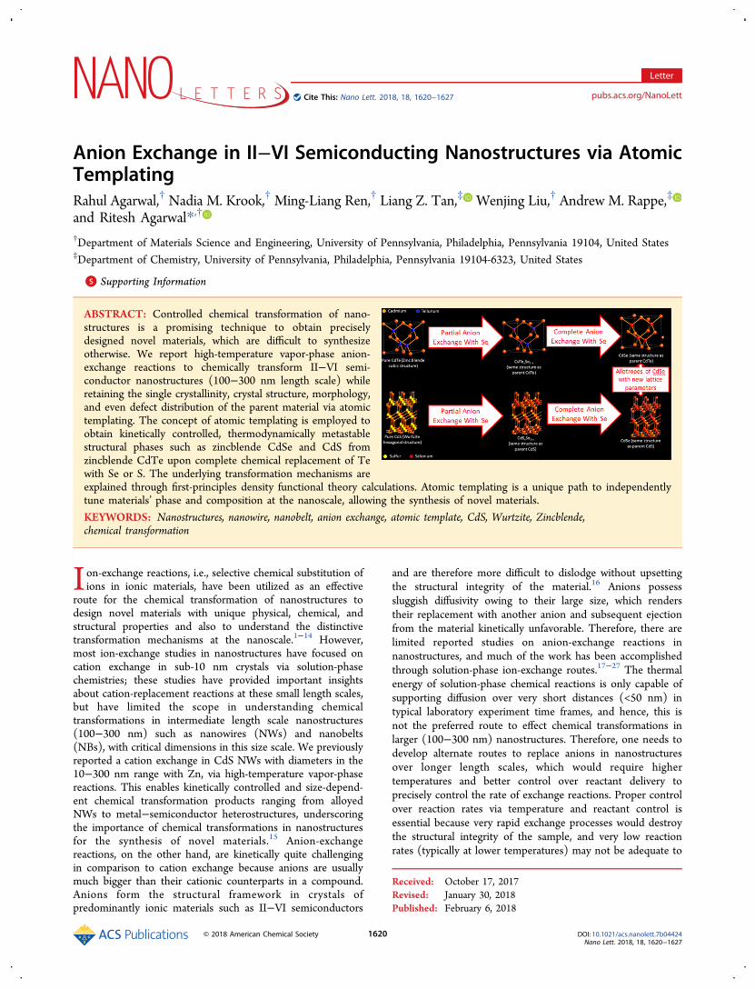
also retain the nature and location of extended lattice defects ina nanostructure upon chemical transformation, assuming thatthe reaction temperature does not exceed the defect annealingtemperature itself. To validate this hypothesis, ZB CdTenanostructures synthesized via the VLS mechanism,53 whichnaturally possess planar growth defects such as twin
Figure 3. Characterization of a twinned NW after undergoing complete anion exchange from ZB CdTe into ZB CdSe. (A) Dark-field TEMmicrograph of a periodically twinned CdTe NW before anion exchange. Upper left inset: SAED pattern confirming the ZB crystal structure,twinning, and <111> growth axis. Bottom right inset: bright-field TEM micrograph of the same NW. (B) Dark-field TEM micrograph of the sameNW after complete anion exchange into CdSe. Upper right inset: SAED pattern confirming retention of the ZB crystal structure, twinning, and<111> growth axis with lattice parameters matching pure ZB CdSe. (C) EDS point scan of the same NW confirming complete chemicaltransformation into CdSe with no residual Te.
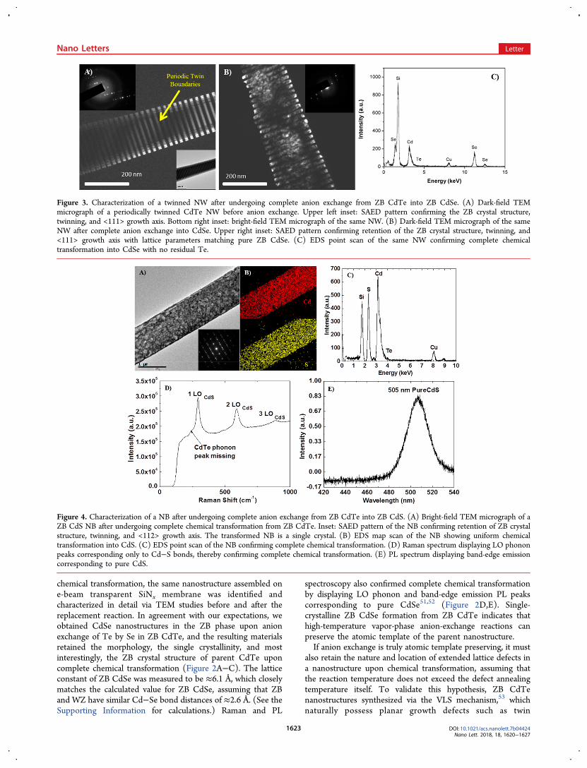
Figure 4. Characterization of a NB after undergoing complete anion exchange from ZB CdTe into ZB CdS. (A) Bright-field TEM micrograph of aZB CdS NB after undergoing complete chemical transformation from ZB CdTe. Inset: SAED pattern of the NB confirming retention of ZB crystalstructure, twinning, and <112> growth axis. The transformed NB is a single crystal. (B) EDS map scan of the NB showing uniform chemicaltransformation into CdS. (C) EDS point scan of the NB confirming complete chemical transformation. (D) Raman spectrum displaying LO phononpeaks corresponding only to Cd−S bonds, thereby confirming complete chemical transformation. (E) PL spectrum displaying band-edge emissioncorresponding to pure CdS.
Nano Letters Letter
DOI: 10.1021/acs.nanolett.7b04424Nano Lett. 2018, 18, 1620−1627
1623

boundaries54 (characterization details in Supporting Informa-tion), were chosen for an anion-exchange reaction with Se(reaction temperature, 450 °C). The same nanostructure wascharacterized before and after the anion-exchange reaction tostudy the evolution of defects and their distribution uponchemical transformation (Figure 3A). Supporting our hypoth-esis of atomic templating, the resulting NW not only retainedthe single-crystalline ZB crystal structure but also the periodictwin boundaries of the parent material upon undergoingcomplete chemical transformation into CdSe (Figure 3B,C).These results in addition to providing important details aboutthe chemical transformation mechanism (discussed later) showthe potential for independently engineering both the chemicalcomposition and structural phase of materials at the nanoscalewhile preserving the defect distribution of the parent material.As mentioned earlier, CdS is thermodynamically stable in the
WZ crystal structure at room temperature and atmosphericpressure, and it is challenging to synthesize larger nanostruc-tures (>100 nm) of CdS in the ZB phase.47−50 Therefore, toobtain large ZB CdS nanostructures, we performed an anion-exchange reaction at 450 °C in ZB CdTe nanostructures with Svapor. Upon performing the reaction, we once again observedcomplete chemical transformation into single-crystalline ZBCdS while retaining the twin boundaries of the parent CdTeNBs (Figure 4). The lattice constant of ZB CdS was measured
to be ≈5.8 Å, which closely matches the calculated value for ZBCdS structure, assuming that ZB and WZ have similar Cd−Sbond distance of ≈2.5 Å. (See the Supporting Information forcalculations.) Successful chemical transformation of ZB CdTeinto ZB CdS while retaining the planar defects is another proofof the lattice preserving nature of the anion-exchange reactionat the nanoscale. The ability to synthesize large nanostructuresof CdS and CdSe in ZB phase highlights the role of anion-exchange-based chemical transformation techniques in phaseengineering of metastable structures, which are challenging toobtain otherwise.To understand the mechanism behind the observed lattice-
framework-preserving chemical transformation, a series ofcontrol experiments were designed to study anion exchangein the WZ CdS model system by introducing Se. The reactionwas kinetically controlled by lowering the reaction temperature,thereby decelerating the transformation kinetics while keepingall other experimental conditions the same, to obtain insightsinto the step-by-step structural and chemical evolution of thenanostructures. Upon performing anion exchange at 300 °C(lowered from 600 °C) in a ≈200 nm diameter WZ CdS NWfor 1 h, we observed that the NW possesses a roughmorphology with periodic protrusions on the surface. Selectedarea electron diffraction (SAED) patterns of the NW reveal asingle-crystalline WZ structure with split diffraction spots
Figure 5. Characterization of nanostructures after undergoing partial anion exchange from CdS to CdSxSe1−x. (A) Bright-field TEM micrograph ofCdSxSe1−x NW after anion exchange at 300 °C. Inset: SAED pattern of the NW confirming single-crystalline WZ structure with split and elongatedspots (red circles). (B) EDS line scan of the same NW confirming the core−shell morphology of the alloyed NW (along the dotted line in A). (C)Bright-field TEM micrograph of CdSxSe1−x NW after anion exchange at 450 °C. Inset: SAED pattern of the NW confirming single-crystalline WZstructure of CdSxSe1−x. (D) EDS line scan of the same NW confirming the core−shell morphology of the alloyed NW (taken along the dotted line inC). (E) Raman spectrum of an alloyed CdSxSe1−x NW showing LO phonon peaks corresponding to both Cd−S and Cd−Se bonds.
Nano Letters Letter
DOI: 10.1021/acs.nanolett.7b04424Nano Lett. 2018, 18, 1620−1627
1624
corresponding to pure WZ CdS and WZ CdSe (Figure 5A). AnEDS line scan along the radial direction indicates that the NWpossesses a compositional gradient, with a Se-rich phase on thesurface and a S-rich phase toward the core, indicating anincomplete anion-exchange reaction (Figure 5B). However,upon performing anion exchange at 450 °C on another ≈200nm diameter WZ CdS NW for 1 h, we again observe roughsurface morphology (smoother than the experiment at 300 °Cbut still much coarser than the reaction at 600 °C), but we finda uniform lattice parameter (no observable diffraction spotsplitting) throughout the material (Figure 5C). The EDS linescan along the radial direction indicates a compositionalgradient. However, the penetration depth of Se toward thecore is higher than was obtained via the anion-exchangereaction performed at 300 °C (Figure 5D). Raman spectros-copy of the NW indicates LO phonon peaks corresponding toboth Cd−S and Cd−Se bonds in a CdSxSe1−x-type alloy inaddition to a sum frequency peak (≈480 cm−1) (Figure 5E)that corresponds to a two-mode behavior from the CdSxSe1−xalloy.36
On the basis of the results obtained from the partial andcomplete chemical transformation in WZ CdS with Se, wepropose the following mechanism for the observed anion-exchange reaction. The reaction temperature influences the rateof the reactant species generated (Se vapor), the kinetic drivingforce for the anion exchange to proceed and the diffusivity ofatoms in the nanostructure, all of which determine the chemicalcomposition and composition distribution of the final product.At a particular reaction temperature, CdS nanostructures(Figure S4A) will be exposed to a constant flux of Se vapor,which will react with CdS at the surface creating domains of aSe-rich CdSxSe1−x alloy through anion exchange, and the excessvapor will condense as amorphous selenium (a-Se) on top,creating protrusions (Figure S4B). Besides anion exchange,incoming Se atoms can occupy the S vacancies sites in CdS,55,56
which is a thermodynamically favorable process. Our first-principles DFT calculations (Supporting Information) showthat the Gibbs free energy for the reaction involving one Seatom in vapor occupying a single S vacancy in WZ CdS is ΔG =−3.01 eV/vacancy at 600 °C, PSe = 100 Torr.Unlike the thermodynamically highly favorable vacancy
occupation reaction, the anion-substitution reaction dependsstrongly on the reaction conditions. Our calculations show thatthe excess Se source vapor and high temperature play a majorrole in driving this reaction. We find that anion substitutionproceeds when S is at a much lower partial pressure than Se:
+ → +WZ CdS Se(gas) WZ CdSe S(gas)
Δ = − °
= = −
G
P P
0.11eV/unit cell at 600 C
100 Torr and 10 Torrrxn
Se S4
In our experiment, the carrier gas (argon flowing at 15SCCM) is capable of instantaneously transporting awayrejected S vapor, which is a byproduct of the forward anion-exchange reaction, acting as an efficient sink for S. This helps inpushing the reaction forward and minimizing the reverse anion-exchange reaction (CdSe transforming into CdS). On the otherhand, at equal partial pressures of Se and S vapors, ourcalculations predict that the complete transformation of WZCdS into WZ CdSe at our reaction temperature (600 °C) viaanion exchange is thermodynamically unfavorable; ΔGrxn =0.932 eV/unit cell at 600 °C, PSe = PS = 100 Torr. This shows
that lowering the S vapor partial pressure as compared to the Sevapor partial pressure reduces the Gibbs free energy of theproducts, making the forward reaction thermodynamicallyfavorable by lowering ΔGrxn from 0.93 to −0.11 eV/unit cellat 600 °C and making the backward reaction kineticallyunfavorable by increasing the activation barrier as a result ofreducing the Gibbs free energy of products. Upon anionexchange, the initial CdSxSe1−x domain size will be directlyproportional and domain spacing will be inversely proportionalto the incoming Se vapor flux, which is dictated by the reactiontemperature. Domain growth of CdSxSe1−x will involve theoutward diffusion of Se2− to the S2−-rich regions while freshSe2− is introduced into the system through a constant anionexchange (Figure S4C). In addition, surface diffusion, which isfaster than bulk diffusion, will lead to the preferential chemicaltransformation at the surface before the core of thenanostructure, thereby creating a core−shell-type morphologyinstead of an axial heterostructure (Figure S4D). Since thesource of Se vapor can be assumed to be infinite with respect tothe limited nanostructure volume available, the anion-exchangereaction and CdSxSe1−x domain growth will continue on thesurface until heating is stopped (Figure S4E). Therefore, at thelowest reaction temperature (300 °C) for 1 h, pure CdS at thecore is preserved and is surrounded by a shell of CdSxSe1−xalloy, which explains the diffraction spot splitting in a SAEDpattern (Figure 5A inset). The rough surface morphology isdue to Cd2+ diffusing from nearby regions into the accumulateda-Se protrusions, thus creating Se-rich CdSxSe1−x in theoutermost shell. At an intermediate reaction temperature(450 °C) for 1 h, the entire nanostructure transforms into aCdSxSe1−x alloy with a radial composition gradient, whichallows the system to relax to an intermediate lattice parameterbetween pure CdS and CdSe. The surface roughness isrelatively lower, since the a-Se condensation rate will be smallerat higher temperatures, and the deposited a-Se will beconsumed at a faster rate through anion exchange. At thehighest reaction temperature (600 °C), the reaction frontproceeds inward all the way to the core, completelytransforming CdS into CdSe with the lowest surface roughness,due to a negligible a-Se deposition on the surface. The mostimportant factor responsible for the observed surface roughnessat 600 °C is lattice expansion by ≈4% as CdS converts intoCdSe and also material sublimation due to a large strain andhigh temperature of the reaction. Since the fully transformednanostructures show no signature of any residual sulfur, it isbelieved to diffuse outward to the surface and then sublimate.At reaction temperatures below 300 °C, no anion exchange isobserved for a similar reaction duration (1 h) since there is notenough kinetic drive to push forward both the chemicalsubstitution reaction and the atomic diffusion. At reactiontemperatures higher than 600 °C, the nanostructures sublimate,possibly owing to a very fast chemical substitution reaction,thereby causing a large-scale bond breaking and therebydestabilizing the anion lattice framework. These experimentsdemonstrate the utility of vapor-phase anion-exchange reactionsin chemically transforming large nanostructures to new singlecomposition or compositionally graded nanomaterials whilepreserving the lattice framework of the parent material. Thisenables the synthesis of metastable phases of materials at thenanoscale while preserving the defect density of the parentmaterial.To summarize, we have demonstrated vapor-phase anion-
exchange reactions as a novel chemical transformation route to
Nano Letters Letter
DOI: 10.1021/acs.nanolett.7b04424Nano Lett. 2018, 18, 1620−1627
1625

independently control materials’ structural phase and compo-sition, thereby allowing us to synthesize well-known com-pounds in metastable stable crystal phases, which can evenretain the defect distribution from the parent nanostructure(Figure 6). In the size range studied in our work (<300 nm),
we did not observe an onset of major defects such as theformation of polycrystalline domains and fracture ordestruction of the observed products, which typically occursin bulk systems. Our work exhibits controlled chemicalreactions at the nanoscale while preserving the structuralintegrity of the material in spite of substituting anions, whichare considered structural pillars in a crystal framework. Thismethod, which we call “atomic templating”, is a promising toolthat can be extended beyond II−VI semiconductors to engineermore exotic materials at the nanoscale for a variety ofelectronic, optical, and energy harvesting and conversionapplications.
■ ASSOCIATED CONTENT*S Supporting InformationThe Supporting Information is available free of charge on theACS Publications website at DOI: 10.1021/acs.nano-lett.7b04424.
TEM, Raman spectroscopy, and photoluminescencespectroscopy experimental details, growth and character-ization details of CdTe nanobelts, anion exchange
experimental details, ZB lattice constant calculations forCdSe and CdS, Figures S1−S4, and first-principlescalculations using density functional theory (PDF)
■ AUTHOR INFORMATIONCorresponding Author*E-mail: [email protected] Z. Tan: 0000-0003-4724-6369Andrew M. Rappe: 0000-0003-4620-6496Ritesh Agarwal: 0000-0002-1289-4334Author ContributionsR.A. and R.A.* conceived and designed the experiments. R.A.,N.M.K., and W.L. optimized the growth conditions andsynthesized the CdS and CdTe nanostructures. R.A. performedthe anion-exchange reaction and the chemical and structuralcharacterization before and after. M-L.R. performed photo-luminescence experiments. L.Z.T and A.M.R performed first-principles density functional theory calculations. R.A. and R.A.*interpreted and analyzed the data. R.A., L.Z.T., A.M.R., andR.A.* cowrote this Letter.NotesThe authors declare no competing financial interest.
■ ACKNOWLEDGMENTSR.A. and L.Z.T. were supported by NSF grant no. DMR-1120901. A.M.R. acknowledges support from the US Depart-ment of Energy under grant no. DE-FG02-07ER46431.Transmission electron microscopy experiments were performedat the Singh Center for Nanotechnology at the University ofPennsylvania. Raman spectroscopy was performed with thesupport of the Nano/Bio Interface Center through the NationalScience Foundation Major Research Instrumentation grant no.DMR-0923245.
■ REFERENCES(1) Demchenko, D. O.; Robinson, R. D.; Sadtler, B.; Erdonmez, C.K.; Alivisatos, A. P.; Wang, L. W. ACS Nano 2008, 2 (4), 627−636.(2) Il Park, W.; Kim, H. S.; Jang, S. Y.; Park, J.; Bae, S. Y.; Jung, M.;Lee, H.; Kim, J. J. Mater. Chem. 2008, 18 (8), 875−880.(3) Jain, P. K.; Amirav, L.; Aloni, S.; Alivisatos, A. P. J. Am. Chem. Soc.2010, 132 (29), 9997−9999.(4) Jeong, U.; Xia, Y.; Yin, Y. Chem. Phys. Lett. 2005, 416 (4−6),246−250.(5) Jeong, U. Y.; Camargo, P. H. C.; Lee, Y. H.; Xia, Y. N. J. Mater.Chem. 2006, 16 (40), 3893−3897.(6) Lee, J. Y.; Kim, D. S.; Park, J. H. Chem. Mater. 2007, 19 (19),4663−4669.(7) Ma, C.; Ding, Y.; Moore, D.; Wang, X.; Wang, Z. L. J. Am. Chem.Soc. 2004, 126 (3), 708−9.(8) Ma, R.; Wang, Y.; Mallouk, T. E. Small 2009, 5 (3), 356−360.(9) Moon, G. D.; Ko, S.; Xia, Y. N.; Jeong, U. ACS Nano 2010, 4 (4),2307−2319.(10) Piccione, B.; Agarwal, R.; Jung, Y.; Agarwal, R. Philos. Mag.2013, 93 (17), 2089−2121.(11) Robinson, R. D.; Sadtler, B.; Demchenko, D. O.; Erdonmez, C.K.; Wang, L. W.; Alivisatos, A. P. Science 2007, 317 (5836), 355−358.(12) Sadtler, B.; Demchenko, D. O.; Zheng, H.; Hughes, S. M.;Merkle, M. G.; Dahmen, U.; Wang, L. W.; Alivisatos, A. P. J. Am.Chem. Soc. 2009, 131 (14), 5285−5293.(13) Son, D. H.; Hughes, S. M.; Yin, Y. D.; Alivisatos, A. P. Science2004, 306 (5698), 1009−1012.(14) Beberwyck, B. J.; Surendranath, Y.; Alivisatos, A. P. J. Phys.Chem. C 2013, 117 (39), 19759−19770.
Figure 6. Schematic representation of the concept of atomictemplating where, for example, polymorphs (WZ and ZB) of acompound (CdSe) can be produced by performing anion exchange instarting compounds with different crystal structures (WZ CdS versusZB CdTe).
Nano Letters Letter
DOI: 10.1021/acs.nanolett.7b04424Nano Lett. 2018, 18, 1620−1627
1626

(15) Zhang, B.; Jung, Y.; Chung, H. S.; Van Vugt, L.; Agarwal, R.Nano Lett. 2010, 10 (1), 149−155.(16) Feng, S. H.; Xu, R. R. Acc. Chem. Res. 2001, 34 (3), 239−247.(17) Dloczik, L.; Engelhardt, R.; Ernst, K.; Fiechter, S.; Sieber, I.;Konenkamp, R. Appl. Phys. Lett. 2001, 78 (23), 3687−3689.(18) Dloczik, L.; Konenkamp, R. Nano Lett. 2003, 3 (5), 651−653.(19) Eliseev, A. A.; Chernysheva, M. V.; Verbitskii, N. I.; Kiseleva, E.A.; Lukashin, A. V.; Tretyakov, Y. D.; Kiselev, N. A.; Zhigalina, O. M.;Zakalyukin, R. M.; Vasiliev, A. L.; Krestinin, A. V.; Hutchison, J. L.;Freitag, B. Chem. Mater. 2009, 21 (21), 5001−5003.(20) Koktysh, D. S.; McBride, J. R.; Dixit, S. K.; Feldman, L. C.;Rosenthal, S. J. Nanotechnology 2007, 18 (49), No. 495607.(21) Shim, H. S.; Shinde, V. R.; Kim, J. W.; Gujar, T. P.; Joo, O. S.;Kim, H. J.; Kim, W. B. Chem. Mater. 2009, 21 (9), 1875−1883.(22) Shinde, V. R.; Gujar, T. P.; Noda, T.; Fujita, D.; Lokhande, C.D.; Joo, O. S. J. Phys. Chem. C 2009, 113 (32), 14179−14183.(23) Xie, Y.; Yan, P.; Lu, J.; Qian, Y. T.; Zhang, S. Y. Chem. Commun.1999, 19, 1969−1970.(24) Liang, H.; Li, L.; Meng, F.; Dang, L.; Zhuo, J.; Forticaux, A.;Wang, Z.; Jin, S. Chem. Mater. 2015, 27 (16), 5702−5711.(25) Li, L.; Yu, Y.; Meng, F.; Tan, Y.; Hamers, R. J.; Jin, S. Nano Lett.2012, 12 (2), 724−731.(26) Fu, Y.; Zhu, H.; Stoumpos, C. C.; Ding, Q.; Wang, J.;Kanatzidis, M. G.; Zhu, X.; Jin, S. ACS Nano 2016, 10 (8), 7963−7972.(27) Nedelcu, G.; Protesescu, L.; Yakunin, S.; Bodnarchuk, M. I.;Grotevent, M. J.; Kovalenko, M. V. Nano Lett. 2015, 15 (8), 5635−5640.(28) Agarwal, R.; Lieber, C. M. Appl. Phys. A: Mater. Sci. Process.2006, 85 (3), 209−215.(29) Hayden, O.; Agarwal, R.; Lieber, C. M. Nat. Mater. 2006, 5 (5),352−6.(30) Piccione, B.; Cho, C. H.; van Vugt, L. K.; Agarwal, R. Nat.Nanotechnol. 2012, 7 (10), 640−5.(31) Piccione, B.; van Vugt, L. K.; Agarwal, R. Nano Lett. 2010, 10(6), 2251−6.(32) van Vugt, L. K.; Piccione, B.; Cho, C. H.; Nukala, P.; Agarwal, R.Proc. Natl. Acad. Sci. U. S. A. 2011, 108 (25), 10050−5.(33) Holt, D. B.; Yacobi, B. G. Extended defects in semiconductors:electronic properties, device effects and structures; Cambridge UniversityPress: Cambridge, 2007.(34) Lange, H.; Artemyev, M.; Woggon, U.; Thomsen, C. Phys. StatusSolidi B 2009, 246 (11−12), 2817−2819.(35) Tell, B.; Damen, T. C.; Porto, S. P. S. Phys. Rev. 1966, 144 (2),771−774.(36) Lu, L.; Xu, X. L.; Liang, W. T.; Lu, H. F. J. Phys.: Condens. Matter2007, 19 (40), 406221.(37) Venugopal, R.; Lin, P. I.; Liu, C. C.; Chen, Y. T. J. Am. Chem.Soc. 2005, 127 (32), 11262−11268.(38) Cox, J. D.; Wagman, D. D.; Medvedev, V. A. CODATA keyvalues for thermodynamics, xiii; Hemisphere Pub. Corp.: New York,1989; p 271.(39) Lawaetz, P. Phys. Rev. B 1972, 5 (10), 4039−4045.(40) Yeh, C. Y.; Lu, Z. W.; Froyen, S.; Zunger, A. Phys. Rev. B:Condens. Matter Mater. Phys. 1992, 46 (16), 10086−10097.(41) Kulakov, M.; Balyakina, I. J. Cryst. Growth 1991, 113 (3−4),653−658.(42) Shan, C. X.; Liu, Z.; Hark, S. K. Appl. Phys. Lett. 2005, 87 (16),163108.(43) Liu, L. P.; Zhuang, Z. B.; Xie, T.; Wang, Y. G.; Li, J.; Peng, Q.;Li, Y. D. J. Am. Chem. Soc. 2009, 131 (45), 16423−16429.(44) Mohamed, M. B.; Tonti, D.; Al-Salman, A.; Chemseddine, A.;Chergui, M. J. Phys. Chem. B 2005, 109 (21), 10533−10537.(45) Capek, R. K.; Moreels, I.; Lambert, K.; De Muynck, D.; Zhao,Q.; Vantomme, A.; Vanhaecke, F.; Hens, Z. J. Phys. Chem. C 2010, 114(14), 6371−6376.(46) Deng, Z. T.; Cao, L.; Tang, F. Q.; Zou, B. S. J. Phys. Chem. B2005, 109 (35), 16671−16675.
(47) Zelaya-Angel, O.; Lozada-Morales, R. Phys. Rev. B: Condens.Matter Mater. Phys. 2000, 62 (19), 13064−13069.(48) Vogel, W.; Urban, J.; Kundu, M.; Kulkarni, S. K. Langmuir 1997,13 (4), 827−832.(49) Jun, Y. W.; Lee, S. M.; Kang, N. J.; Cheon, J. J. Am. Chem. Soc.2001, 123 (21), 5150−5151.(50) Cao, Y. C.; Wang, J. H. J. Am. Chem. Soc. 2004, 126 (44),14336−14337.(51) Islam, S. S.; Rath, S.; Jain, K. P.; Abbi, S. C.; Julien, C.;Balkanski, M. Phys. Rev. B: Condens. Matter Mater. Phys. 1992, 46 (8),4982−4985.(52) Lee, J. S.; Giles, N. C.; Rajavel, D.; Summers, C. J. Phys. Rev. B:Condens. Matter Mater. Phys. 1994, 49 (3), 1668−1676.(53) Agarwal, R.; Zakharov, D. N.; Krook, N. M.; Liu, W.; Berger, J.S.; Stach, E. A.; Agarwal, R. Nano Lett. 2015, 15 (5), 3303−3308.(54) Li, Q.; Gong, X.; Wang, C.; Wang, J.; Ip, K.; Hark, S. Adv. Mater.2004, 16 (16), 1436−1440.(55) Kumar, V.; Kroger, F. J. Solid State Chem. 1971, 3 (3), 387−400.(56) Kumar, V.; Kroger, F. J. Solid State Chem. 1971, 3 (3), 406−410.
Nano Letters Letter
DOI: 10.1021/acs.nanolett.7b04424Nano Lett. 2018, 18, 1620−1627
1627