anomalous plasmon resonance from confined diffusive...
TRANSCRIPT
Anomalous plasmon resonance from confined diffusive charges: high quality and tunability from mid to far infrared wavebands YU GU, XIAOMING LI, JUN CHEN AND HAIBO ZENG* Institute of Optoelectronics and Nanomaterials, Jiangsu Key Laboratory of Advanced Micro and Nano Materials and Technology, College of Material Science and Engineering, Nanjing University of Science and Technology, Nanjing 210094, China *[email protected]
Abstract: For heavily-doped semiconductor nanocrystals, a new class of plasmonic materials, the abundant dopants provide sufficient free carriers, but also act as scattering impurities, which have been limiting the merit of localized surface plasmon resonance (LSPR). To resolve this intrinsic contradiction, we propose a core-shell (heavily-lightly doped) semiconductor nanosystem to generate plasmon resonance from the highly mobile diffusive charges rather than the strongly scattered charges. We develop a complete theory to describe the spatial distribution of the diffusive charges as well as their resonance under the light excitation and predict a LSPR tunable from mid to far infrared band with a 15-fold field enhancement near the resonance. Meanwhile, the physical nature of such LSPR, which is different from the bonding and antibonding plasmon mode in typical core-shell structures, was revealed by studying the polarization charge distribution. Hopefully, these results can help realize high quality plasmonic structures for applications in infrared waveband. © 2016 Optical Society of America
OCIS codes: (250.5403) Plasmonics; (240.6680) Surface plasmons; (160.6000) Semiconductor materials; (260.5740) Resonance.
References and links 1. S. A. Maier, Plasmonics: Fundamentals and Applications (Springer, 2007), pp. xxiv. 2. P. Drude, “Zur elektronentheorie der metalle,” Ann. Phys. 306(3), 566–613 (1900). 3. T. Klar, M. Perner, S. Grosse, G. von Plessen, W. Spirkl, and J. Feldmann, “Surface-plasmon resonances in
single metallic nanoparticles,” Phys. Rev. Lett. 80(19), 4249–4252 (1998). 4. C. Sönnichsen, T. Franzl, T. Wilk, G. von Plessen, J. Feldmann, O. Wilson, and P. Mulvaney, “Drastic reduction
of plasmon damping in gold nanorods,” Phys. Rev. Lett. 88(7), 077402 (2002). 5. P. Mulvaney, “Surface plasmon spectroscopy of nanosized metal particles,” Langmuir 12(3), 788–800 (1996). 6. K. L. Kelly, E. Coronado, L. L. Zhao, and G. C. Schatz, “The optical properties of metal nanoparticles: The
influence of size, shape, and dielectric environment,” J. Phys. Chem. B 107(3), 668–677 (2003). 7. X. Liu and M. T. Swihart, “Heavily-doped colloidal semiconductor and metal oxide nanocrystals: an emerging
new class of plasmonic nanomaterials,” Chem. Soc. Rev. 43(11), 3908–3920 (2014). 8. J. M. Luther, P. K. Jain, T. Ewers, and A. P. Alivisatos, “Localized surface plasmon resonances arising from free
carriers in doped quantum dots,” Nat. Mater. 10(5), 361–366 (2011). 9. X. Huang, I. H. El-Sayed, W. Qian, and M. A. El-Sayed, “Cancer cell imaging and photothermal therapy in the
near-infrared region by using gold nanorods,” J. Am. Chem. Soc. 128(6), 2115–2120 (2006). 10. Z. Zhu, Y. Zou, W. Hu, Y. Li, Y. Gu, B. Cao, N. Guo, L. Wang, J. Song, and S. Zhang, “Near‐Infrared
Plasmonic 2D Semimetals for Applications in Communication and Biology,” Adv. Funct. Mater. 26, 1793–1802 (2016).
11. M. Ringler, A. Schwemer, M. Wunderlich, A. Nichtl, K. Kürzinger, T. A. Klar, and J. Feldmann, “Shaping emission spectra of fluorescent molecules with single plasmonic nanoresonators,” Phys. Rev. Lett. 100(20), 203002 (2008).
12. P. Anger, P. Bharadwaj, and L. Novotny, “Enhancement and quenching of single-molecule fluorescence,” Phys. Rev. Lett. 96(11), 113002 (2006).
13. M. Kauranen and A. V. Zayats, “Nonlinear plasmonics,” Nat. Photonics 6(11), 737–748 (2012). 14. H. A. Atwater and A. Polman, “Plasmonics for improved photovoltaic devices,” Nat. Mater. 9(3), 205–213
(2010). 15. Y. Gu and K. G. Kornev, “Plasmon enhanced direct and inverse Faraday effects in non-magnetic
nanocomposites,” J. Opt. Soc. Am. B 27(11), 2165–2173 (2010).
Vol. 24, No. 26 | 26 Dec 2016 | OPTICS EXPRESS 29908
#275819 Journal © 2016
http://dx.doi.org/10.1364/OE.24.029908 Received 20 Sep 2016; revised 11 Nov 2016; accepted 11 Nov 2016; published 15 Dec 2016
16. L.-Y. Chen, Z.-X. Tang, J.-L. Gao, D.-Y. Li, C.-X. Lei, Z.-Z. Cheng, S.-L. Tang, and Y.-W. Du, “Fano resonance and magneto-optical Kerr rotaion in periodic Co/Ni complex plasmonic nanostructure,” Chin. Phys. B 25(11), 113301 (2016).
17. L. W. Chou, N. Shin, S. V. Sivaram, and M. A. Filler, “Tunable Mid-Infrared Localized Surface Plasmon Resonances in Silicon Nanowires,” J. Am. Chem. Soc. 134(39), 16155–16158 (2012).
18. I. Kriegel, C. Jiang, J. Rodríguez-Fernández, R. D. Schaller, D. V. Talapin, E. da Como, and J. Feldmann, “Tuning the Excitonic and Plasmonic Properties of Copper Chalcogenide Nanocrystals,” J. Am. Chem. Soc. 134(3), 1583–1590 (2012).
19. R. Buonsanti, A. Llordes, S. Aloni, B. A. Helms, and D. J. Milliron, “Tunable Infrared Absorption and Visible Transparency of Colloidal Aluminum-Doped Zinc Oxide Nanocrystals,” Nano Lett. 11(11), 4706–4710 (2011).
20. Y. Zhao, H. Pan, Y. Lou, X. Qiu, J. Zhu, and C. Burda, “Plasmonic Cu(2-x)S nanocrystals: optical and structural properties of copper-deficient copper(I) sulfides,” J. Am. Chem. Soc. 131(12), 4253–4261 (2009).
21. A. Berrier, R. Ulbricht, M. Bonn, and J. G. Rivas, “Ultrafast active control of localized surface plasmon resonances in silicon bowtie antennas,” Opt. Express 18(22), 23226–23235 (2010).
22. H. Matsui, S. Furuta, and H. Tabata, “Role of electron carriers on local surface plasmon resonances in doped oxide semiconductor nanocrystals,” Appl. Phys. Lett. 104(21), 211903 (2014).
23. T. Makino, Y. Segawa, A. Tsukazaki, A. Ohtomo, and M. Kawasaki, “Electron transport in ZnO thin films,” Appl. Phys. Lett. 87(2), 022101 (2005).
24. D. Chattopadhyay and H. J. Queisser, “Electron-Scattering by Ionized Impurities in Semiconductors,” Rev. Mod. Phys. 53(4), 745–768 (1981).
25. E. Della Gaspera, A. S. R. Chesman, J. van Embden, and J. J. Jasieniak, “Non-injection synthesis of doped zinc oxide plasmonic nanocrystals,” ACS Nano 8(9), 9154–9163 (2014).
26. D. Schurig, J. J. Mock, B. J. Justice, S. A. Cummer, J. B. Pendry, A. F. Starr, and D. R. Smith, “Metamaterial electromagnetic cloak at microwave frequencies,” Science 314(5801), 977–980 (2006).
27. J. B. Pendry, D. Schurig, and D. R. Smith, “Controlling electromagnetic fields,” Science 312(5781), 1780–1782 (2006).
28. U. Leonhardt, “Optical conformal mapping,” Science 312(5781), 1777–1780 (2006). 29. J. Valentine, J. Li, T. Zentgraf, G. Bartal, and X. Zhang, “An optical cloak made of dielectrics,” Nat. Mater. 8(7),
568–571 (2009). 30. D. A. Neamen, Semiconductor Physics and Devices: Basic Principles, 4th ed. (McGraw-Hill, 2012), pp. xxiv. 31. J. D. Jackson, Classical electrodynamics, 3rd ed. (Wiley, 1999), pp. xxi. 32. L. D. Landau, E. M. Lifshitz and L. P. Pitaevskiĭ, Electrodynamics of Continuous Media, 2nd ed., (Pergamon,
1984), pp. xiii. 33. C. F. Bohren and D. R. Huffman, Absorption and # of Light by Small Particles (Wiley, 1983), pp. xiv. 34. I. B. Kobiakov, “Elastic, Piezoelectric and Dielectric-Properties of Zno and Cds Single-Crystals in a Wide-
Range of Temperatures,” Solid State Commun. 35(3), 305–310 (1980). 35. F. C. Chiu, P. W. Li, and W. Y. Chang, “Reliability characteristics and conduction mechanisms in resistive
switching memory devices using ZnO thin films,” Nanoscale Res. Lett. 7(1), 178 (2012). 36. R. J. Goldston and P. H. Rutherford, Introduction to Plasma Physics (Institute of Physics Pub., 1995), pp. xvii. 37. E. Prodan, C. Radloff, N. J. Halas, and P. Nordlander, “A hybridization model for the plasmon response of
complex nanostructures,” Science 302(5644), 419–422 (2003). 38. R. D. Averitt, D. Sarkar, and N. J. Halas, “Plasmon resonance shifts of Au-coated Au2S nanoshells: Insight into
multicomponent nanoparticle growth,” Phys. Rev. Lett. 78(22), 4217–4220 (1997). 39. Y. Yang, J. L. Shi, G. Kawamura, and M. Nogami, “Preparation of Au-Ag, Ag-Au core-shell bimetallic
nanoparticles for surface-enhanced Raman scattering,” Scr. Mater. 58(10), 862–865 (2008). 40. S. Zhou, X. Pi, Z. Ni, Y. Ding, Y. Jiang, C. Jin, C. Delerue, D. Yang, and T. Nozaki, “Comparative Study on the
Localized Surface Plasmon Resonance of Boron- and Phosphorus-Doped Silicon Nanocrystals,” ACS Nano 9(1), 378–386 (2015).
41. B. H. Bairamov, A. Heinrich, G. Irmer, V. V. Toporov, and E. Ziegler, “Raman-Study of the Phonon Halfwidths and the Phonon Plasmon Coupling in Zno,” Phys. Status Solidi, B Basic Res. 119(1), 227–234 (1983).
42. K. Ding, Q. C. Hu, W. W. Lin, J. K. Huang, and F. Huang, “Longitudinal optical phonon-plasmon coupled modes of degenerate Al-doped ZnO films,” Appl. Phys. Lett. 101(3), 031908 (2012).
43. H. Yan, T. Low, F. Guinea, F. Xia, and P. Avouris, “Tunable phonon-induced transparency in bilayer graphene nanoribbons,” Nano Lett. 14(8), 4581–4586 (2014).
44. W. Wan, X. Yang, and J. Gao, “Strong coupling between mid-infrared localized plasmons and phonons,” Opt. Express 24(11), 12367–12374 (2016).
45. F. Wang and Y. R. Shen, “General properties of local plasmons in metal nanostructures,” Phys. Rev. Lett. 97(20), 206806 (2006).
46. C. Deeb, R. Bachelot, J. Plain, A. L. Baudrion, S. Jradi, A. Bouhelier, O. Soppera, P. K. Jain, L. Huang, C. Ecoffet, L. Balan, and P. Royer, “Quantitative Analysis of Localized Surface Plasmons Based on Molecular Probing,” ACS Nano 4(8), 4579–4586 (2010).
47. M. Kerker, The Scattering of Light, and Other Electromagnetic Radiation, Physical chemistry, a series of monographs, 16 (Academic Press, 1969), pp. xv.
Vol. 24, No. 26 | 26 Dec 2016 | OPTICS EXPRESS 29909
48. J.-P. Schäfer, “Implementierung und Anwendung analytischer und numerischer Verfahren zur Lösung der Maxwellgleichungen für die Untersuchung der Lichtausbreitung in biologischem Gewebe,” (Universität Ulm, 2011).
49. J. Schäfer, S. C. Lee, and A. Kienle, “Calculation of the near fields for the scattering of electromagnetic waves by multiple infinite cylinders at perpendicular incidence,” J Quant Spectrosc Ra 113(16), 2113–2123 (2012).
1. Introduction In metals and heavily-doped semiconductors, free charges can oscillate collectively under the irradiation of light and such collective oscillations are defined as “plasmon” [1]. Meanwhile, the ions fixed at the lattice points are typically treated as a continuous matrix which only resists the oscillation via a velocity-dependent “friction” force [2]. When the scale of the material is decreased to nanometers (smaller than the wavelength of light), the surface confined free charges could oscillate resonantly at certain light frequencies. This phenomenon is called Localized Surface Plasmon Resonance (LSPR) and has been extensively studied for both noble metal and heavily-doped semiconductor nanocrystals [3–8]. Near the resonance, an intense light absorption by the particle as well as significant local field enhancement can be observed. Due to such features, LSPR has been widely used in various fields such as photothermal therapy [9, 10], molecular fluorescence [11, 12], nonlinear optics [13], optoelectronics [14], magneto-plasmonics [15, 16] etc.
Different from traditional noble metal nanostructures, the LSPR of heavily doped semiconductor nanocrystals has caught great attentions only in recent years [7, 8, 17, 18]. The main advantage of semiconductor nanocrystals lies in the tunability of their carrier concentrations in a wide range. Varying the carrier concentrations in the range of 1017 cm−3 ~1021 cm−3, one expects to achieve LSPR from THz wave band all the way up to the near infrared region [7, 17–19]. Up until now, LSPR has been realized in semiconductors like Si, metal oxides (ZnO, In2O3), copper chalcogenides etc. Meanwhile, the particular carrier concentration can be achieved with different methods including self-doping [18, 20], extrinsic-doping [17, 19], optical pumping [21] etc. It can be seen that the current researches have been mainly focusing on exploring new semiconducting materials as well as searching for better methods of tuning the carrier concentration for LSPR applications. However, in all related researches, increasing the doping concentration is always accompanied by creating additional ionized impurities. In particular, at high carrier concentrations (n>1018 cm−3), ionized impurity scattering would significantly increase the collision frequency (damping coefficient) γ = e/(meμ) (e: elementary charge, me: effective mass of the carriers, μ: carrier mobility) [22–24], leading to a rather weak resonance [22, 25]. It seems impossible to achieve high carrier concentrations without causing significant damping. This problem has been hindering the further development of the LSPR for semiconductor nanocrystals.
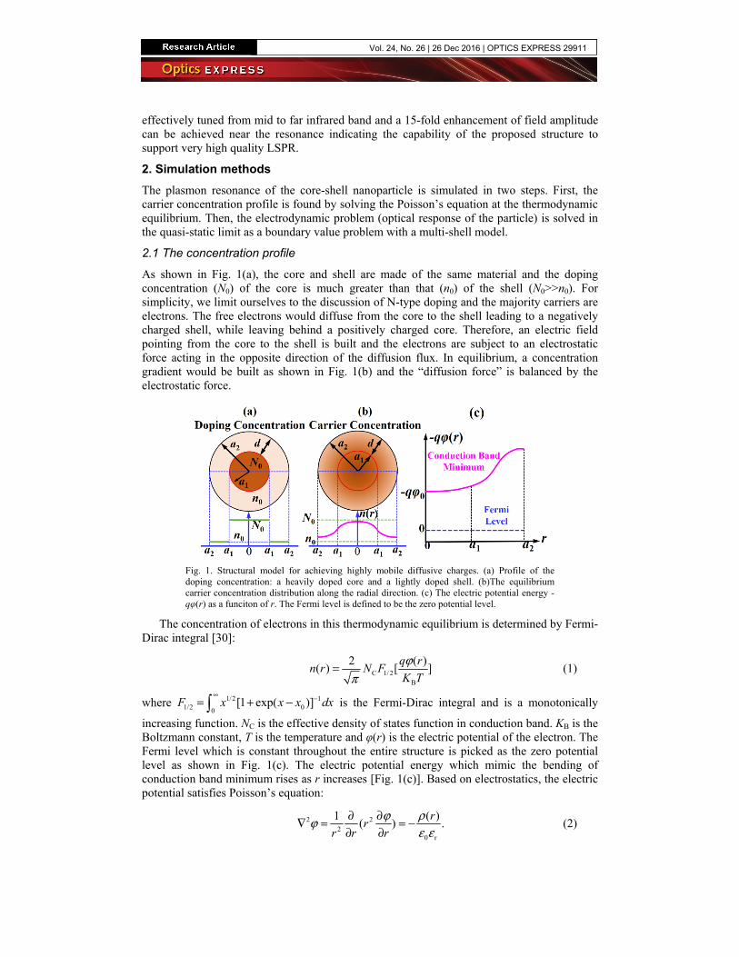
To resolve this problem, we propose to exploit the highly mobile diffusive charges, rather than the strongly scattered charges, to generate plasmon resonance. A semiconductor particle [Fig. 1(a)] with a heavily doped core and a lightly doped shell is capable of providing such highly mobile diffusive charges. As will be explained later, being confined by the shell, the diffusive electrons forms a concentration gradient [Fig. 1(b)] and the core-shell particle can be treated as a peculiar material with gradually-varying optical properties. Structures with gradient index has been extensively studied in transformation optics for designing metamaterials to realize cloaks from microwave to optical frequencies [26–29]. Those structures typically rely on the geometrical design of the unit cell and the gradient is created by introducing the gradual variation of the geometrical parameters of the cells or their packing density. To the best of our knowledge, very limited works can be found on an isotropic spherical particle with intrinsic gradient index due to the diffusion of charge carriers. We thereby provide a theoretical analysis of the anomalous LSPR of this novel structure here. Our theoretical results suggest the emergence of a unique triple peak spectrum due to the diffusive charges. The physical origins of these three peaks are revealed by studying the polarization charge density. More importantly, the resonance frequency can be very
Vol. 24, No. 26 | 26 Dec 2016 | OPTICS EXPRESS 29910
effectively tuned from mid to far infrared band and a 15-fold enhancement of field amplitude can be achieved near the resonance indicating the capability of the proposed structure to support very high quality LSPR.
2. Simulation methods The plasmon resonance of the core-shell nanoparticle is simulated in two steps. First, the carrier concentration profile is found by solving the Poisson’s equation at the thermodynamic equilibrium. Then, the electrodynamic problem (optical response of the particle) is solved in the quasi-static limit as a boundary value problem with a multi-shell model.
2.1 The concentration profile
As shown in Fig. 1(a), the core and shell are made of the same material and the doping concentration (N0) of the core is much greater than that (n0) of the shell (N0>>n0). For simplicity, we limit ourselves to the discussion of N-type doping and the majority carriers are electrons. The free electrons would diffuse from the core to the shell leading to a negatively charged shell, while leaving behind a positively charged core. Therefore, an electric field pointing from the core to the shell is built and the electrons are subject to an electrostatic force acting in the opposite direction of the diffusion flux. In equilibrium, a concentration gradient would be built as shown in Fig. 1(b) and the “diffusion force” is balanced by the electrostatic force.
Fig. 1. Structural model for achieving highly mobile diffusive charges. (a) Profile of the doping concentration: a heavily doped core and a lightly doped shell. (b)The equilibrium carrier concentration distribution along the radial direction. (c) The electric potential energy -qφ(r) as a funciton of r. The Fermi level is defined to be the zero potential level.
The concentration of electrons in this thermodynamic equilibrium is determined by Fermi-Dirac integral [30]:
C 1/ 2B
2 ( )( ) [ ]
q rn r N F
K T
ϕπ
= (1)
where 1/2 11/2 00
[1 exp( )]∞ −= + −F x x x dx is the Fermi-Dirac integral and is a monotonically
increasing function. NC is the effective density of states function in conduction band. KB is the Boltzmann constant, T is the temperature and φ(r) is the electric potential of the electron. The Fermi level which is constant throughout the entire structure is picked as the zero potential level as shown in Fig. 1(c). The electric potential energy which mimic the bending of conduction band minimum rises as r increases [Fig. 1(c)]. Based on electrostatics, the electric potential satisfies Poisson’s equation:
2 22
0 r
1 ( )( ) .
rr
r rr
ϕ ρϕε ε
∂ ∂∇ = = −∂ ∂
(2)
Vol. 24, No. 26 | 26 Dec 2016 | OPTICS EXPRESS 29911
where ρ is the space charge density and εr is the static relative permittivity of the material. ρ(r) is related to the electron concentration as follows:
0 1
0 1 2
[ ( )] ( )( ) .
[ ( ) ] ( ) ( )
q N n r r ar
q n r n qn r a r aρ
− <= − − ≈ − < <
(3)
The contributions from holes and negatively charged acceptors are ignored. As seen from Eqs. (1) and (3), ρ(r) can be written in terms of φ(r). Consequently, the second order ordinary differential Eq. (2) can be solved iteratively as an initial value problem so that φ(r) can be found and the electron concentration distribution is then calculated by Eq. (1). (see Appendix A for details)
2.2 The optical response
The radial concentration gradient of electrons described by Eq. (1) leads to a plasma frequency in the following form: ωp(r) = [n(r)e2/meε0]
1/2 (me the effective mass of electrons) and the material acquires a spatially varying permittivity ε(ω,r) defined by Drude model [1].
2
2
( )( , ) p r
ri
ωε ω ε
ω γω∞= −+
(4)
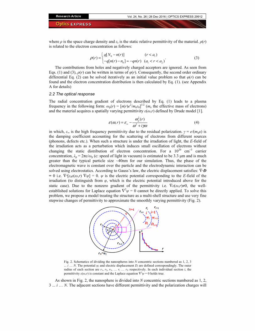
in which, ε∞ is the high frequency permittivity due to the residual polarization. γ = e/(meμ) is the damping coefficient accounting for the scattering of electrons from different sources (phonons, defects etc.). When such a structure is under the irradiation of light, the E-field of the irradiation acts as a perturbation which induces small oscillation of electrons without changing the static distribution of electron concentration. For a 1020 cm−3 carrier concentration, λp = 2πc/ωp (c: speed of light in vacuum) is estimated to be 3.3 μm and is much greater than the typical particle size ~40nm for our simulation. Thus, the phase of the electromagnetic wave is constant over the particle and the electrodynamic interaction can be solved using electrostatics. According to Gauss’s law, the electric displacement satisfies: ∇·D = 0 i.e. ∇·[ε0ε(ω,r) ∇ψ] = 0. ψ is the electric potential corresponding to the E-field of the irradiation (to distinguish from φ, which is the electric potential introduced above for the static case). Due to the nonzero gradient of the permittivity i.e. ∇ε(ω,r)≠0, the well-established solutions for Laplace equation ∇2ψ = 0 cannot be directly applied. To solve this problem, we propose a model treating the structure as a multi-shell structure and use very fine stepwise changes of permittivity to approximate the smoothly varying permittivity (Fig. 2).
Fig. 2. Schematics of dividing the nanospheres into N concentric sections numbered as 1, 2, 3 ... i … N. The potential ψi and electric displacement Di are defined correspondingly. The outer radius of each section are r1, r2, r3, … ri … rN respectively. In each individual section i, the permittivity ε(ω,r) is constant and the Laplace equation ∇2ψ = 0 holds true.
As shown in Fig. 2, the nanosphere is divided into N concentric sections numbered as 1, 2, 3 ... i … N. The adjacent sections have different permittivity and the polarization charges will
Vol. 24, No. 26 | 26 Dec 2016 | OPTICS EXPRESS 29912
be accumulated on all the boundaries ri. In each infinitesimal section, ∇ε(ω,r) is zero and Laplace equation ∇2ψ = 0 holds true. Therefore, keeping only the dipolar mode, the general solution of the problem for the ith section is written as [31, 32]:
0 3( , ) ( )( )i
i irr
βψ θ α= − ⋅ −E r (5)
where E0 is electric component of the irradiation of light. All the coefficients αi and βi can be found by matching potential ψi and normal component of electric displacement Di on each individual boundaries ri. (see Appendix B for details). Based on the coefficient βN + 1, both the scattering (Cscat), absorption (Cabs) as well as the extinction (Cext = Cabs + Cscat) cross sections of a single particle can be calculated. In the quasi-static limit, the size parameter 2πa/λ (a: size of the particle, λ: wavelength of the light) is small, typically less than 10−2. Since Cscat/Cabs is proportional to (2πa/λ)3 [33], the scattering cross section is negligibly small and the following relation holds true Cext = Cabs. Therefore, throughout the paper, only absorption cross section would be considered and it is written as [1, 33]:
abs 1Im(4 ) ( / ).N mC k k cπβ ε ω+= = (6)
in which, 4πβN+1 is the polarizability of the particle which acts as an oscillating dipole with the dipole moment p = ε0εm(4πβN+1)E0. The electric field outside the particle is the superposition of the field E0 and the field generated by the dipole p. The validity of this proposed simulation method is also verified by running a test simulation. The results show excellent agreement with the extract solutions based on Mie theory (see Fig. 8 in Appendix B for details).
Table 1. Parameters used for simulations.
Parameter value Parameter value a1 (nm) 20 εr 10.5 [34] d (nm) 2~20 ε∞ 3.7 [25] T (K) 300 εm 2.5 N0 ( × 1020cm−3) 1 Nc ( × 1018cm−3) 4 [35] me ( × m0) 0.24 [25] μ1 (cm2/V/s) 20 [23] μ2 (cm2/V/s) 400 [23] Notes: a1: core radius; d: shell thickness; N0: doping concentration; T: temperature; εm: medium permittivity; εr: static permittivity; ε∞: high frequency permittivity; Nc: effective density of states; me: effective mass; m0: free electron mass; μ1: electron mobility in the core; μ2: electron mobility in the shell. Values of me, εr, ε∞, Nc, μ1, μ2 were taken from literatures and the corresponding references are added right next to the values.
For all simulations, we pick ZnO as the modeling material because the ZnO nanocrystals can be synthesized and heavily-doped by a facile, non-injection method [25]. The simulation parameters are summarized in Table 1. It is worth noting that any semiconductor materials can be simulated following the methods introduced above as long as all the material parameters (εr, ε∞, me, Nc, μ1, μ2) are known. In this paper, we would focus on revealing the novelty and physical natures of the resonances rather than exploring different materials for the resonance. Meanwhile, the mobility of electrons in the shell (μ = 400 cm2/V/s) is directly taken from the experimentally measured values presented in [23] and should be achievable experimentally for the nanocrystals. For this value, the mean free path of electrons can be calculated as: lF = (3πn)1/3μħ/e≈26nm (ħ: the reduced Planck constant, n: the electron concentration is taken as 1020 cm−3) [22]. Therefore, lF is smaller than the particle size 2(a1 + d) and the surface scattering which is only significant when the particle size is much smaller than the mean free path can be safely ignored in our simulation.
Vol. 24, No. 26 | 26 Dec 2016 | OPTICS EXPRESS 29913
3. Results and discussions
3.1 Electron concentration and the absorption spectrum
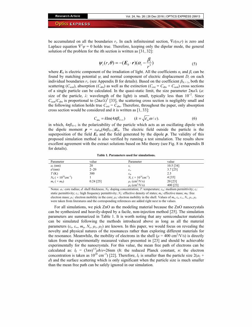
Fig. 3. Electron concentration distribution along the radial direction. The inner radius a1 = 20 nm, doping concentration N0 = 1020 cm−3 and the thickness of the shell d is varied from 2 to 10 nm. Position r is normalized by the outer radius a2. The filled circles show the boundary between the core and shell (r = a1). The inset illustrates the electron concentration at the shell surface and the corresponding plasma wavelength as a function of the shell thickness (from 2 to 20 nm).
The electron concentration n(r) along the radial direction is shown in Fig. 3. The concentration varies most significantly in the vicinity of the boundary between the core and the shell (r = a1, marked by the filled circle in the graph). For the very high doping concentrations (N0 = 1020 cm−3), the Debye length lD = (ε0εrKBT/N0e
2)1/2 is estimated as 0.39nm and is much smaller than the core radius a1 (20 nm). Since lD characterizes how far the electrostatic effects from the charges persist [36], the electron concentration near the particle center remains almost unperturbed by the shell. For the sake of simplicity, we will only discuss the case lD<<a1 throughout the paper. On the other hand, Fig. 3 also shows an efficient manipulation of the concentration profile by varying d. In particular, as illustrated by the inset, the electron concentration n(r) at the particle surface (r = a2) and the corresponding plasma wavelength λp can be very effectively tuned in a wide range. As will be shown later, this efficient control of the plasma wavelength λp on the surface would result in a plasmon resonance which is very sensitive to the shell thickness d.
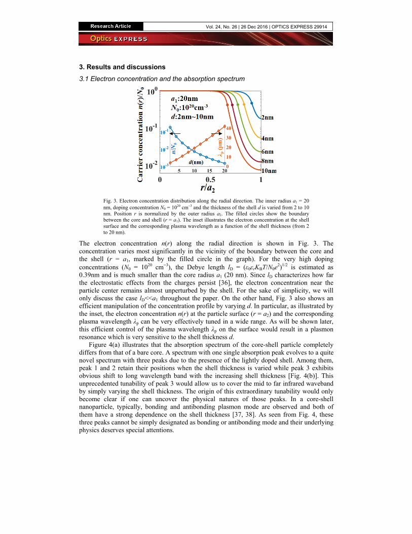
Figure 4(a) illustrates that the absorption spectrum of the core-shell particle completely differs from that of a bare core. A spectrum with one single absorption peak evolves to a quite novel spectrum with three peaks due to the presence of the lightly doped shell. Among them, peak 1 and 2 retain their positions when the shell thickness is varied while peak 3 exhibits obvious shift to long wavelength band with the increasing shell thickness [Fig. 4(b)]. This unprecedented tunability of peak 3 would allow us to cover the mid to far infrared waveband by simply varying the shell thickness. The origin of this extraordinary tunability would only become clear if one can uncover the physical natures of those peaks. In a core-shell nanoparticle, typically, bonding and antibonding plasmon mode are observed and both of them have a strong dependence on the shell thickness [37, 38]. As seen from Fig. 4, these three peaks cannot be simply designated as bonding or antibonding mode and their underlying physics deserves special attentions.
Vol. 24, No. 26 | 26 Dec 2016 | OPTICS EXPRESS 29914
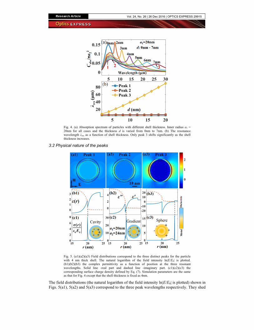
Fig. 4. (a) Absorption spectrum of particles with different shell thickness. Inner radius a1 = 20nm for all cases and the thickness d is varied from 0nm to 7nm. (b) The resonance wavelength λres as a function of shell thickness. Only peak 3 shifts significantly as the shell thickness increases.
3.2 Physical nature of the peaks
Fig. 5. (a1)(a2)(a3) Field distributions correspond to the three distinct peaks for the particle with 4 nm thick shell. The natural logarithm of the field intensity ln|E/E0| is plotted. (b1)(b2)(b3) the complex permittivity as a function of position at the three resonant wavelengths. Solid line -real part and dashed line -imaginary part. (c1)(c2)(c3) the corresponding surface charge density defined by Eq. (7). Simulation parameters are the same as that for Fig. 4 except that the shell thickness is fixed as 4nm.
The field distributions (the natural logarithm of the field intensity ln|E/E0| is plotted) shown in Figs. 5(a1), 5(a2) and 5(a3) correspond to the three peak wavelengths respectively. They shed
Vol. 24, No. 26 | 26 Dec 2016 | OPTICS EXPRESS 29915
light on the nature of those three peaks. Peak 1 and 2 correspond to resonances arising in the vicinity of the inner surface of the shell because the electric field is mostly enhanced near this interface [Figs. 5(a1) and 5(a2)]. Since the local electron concentration distribution near this interface weakly depends on the shell thickness as illustrated in Fig. 3, peak 1 and 2 are expected to retain their positions upon the variation of the shell thickness. On the other hand, peak 3 is attributed to the outer boundary of the shell [Fig. 5(a3)] where the electron concentration varies rather significantly for different shell thickness (Fig. 3) leading to a strong dependence of peak 3 on the shell thickness. Meanwhile, since the resonance relies on the outer shell, the rather strong oscillator strength of peak 3 should also be attributed to the low damping coefficient (high mobility μ = 400 cm2/V/s) of electrons in the shell. To better understand the nature of these three peaks, we calculate the polarization charge density σ(ri) at difference interfaces ri according to Gauss’s Law:
( ) 1 1
0 1
( )i i
i i i i i i
ir r r r
r
r r r
σ ψ ψ ε ε ψε ε
+ +
+= =
∂ ∂ − ∂= − =
∂ ∂ ∂ (7)
The last equation originates from the continuity of the normal component of the electric displacement D. The radial derivative of the potential ψ in Eq. (7) is taken along the direction of the electric field of the light. Figures 5(c1)-5(c3) show that the charge density functions at the three peak wavelengths are quite different. Peak 1 is mainly attributed to the surface charges accumulated at r = a1 = 20 nm (inner shell surface) while peak 3 mainly arises from the charges at r = a2 = 24 nm (outer shell surface). At these two interfaces, surface polarization charge appears due to the abrupt change of permittivity which is similar to conventional LSPR as illustrated in Fig. 5(b1), 5(c1) and 5(b3), 5(c3) (the abrupt change of permittivity at the core and shell interface is due to the difference in damping coefficient γ). Peak 2 is rather special because majority of the surface charges appear at the surface where the real part ε′ and imaginary part ε” of the permittivity goes to zero [Fig. 5(b2) and 5(c2)]. It is a unique feature due to the smooth transition from “metal” (ε′<0) to “dielectrics” (ε′>0) inside the core-shell structure. The emerging of polarization charges at the εi = 0 interface agrees with Eq. (7) which indicates that obvious surface charges would only appear if |εi+1|~0 since |εi+1-εi|~0 for the smoothly-varying permittivity. It also explains the fact that no obvious charges appear at the interface where ε′ flips sign but ε” is still large [the ε′ = 0 interface shown in Fig. 5(b1) and 5(c1)].
3.3 Comparison with other nanostructures
Combining the charge distribution and the spatially varying permittivity shown in Fig. 5, one can better identify the three plasmon modes. Strictly speaking, all the three resonances are hybridized plasmon modes since surface charges are distributed on a series of interfaces rather than being restricted to a single one. In a typical core-shell structure, the bonding and anti-bonding modes are observed due to the coupling between the two plasmons arising at the inner and outer interfaces of the shell [37]. The one at the inner surface is named as “cavity plasmon” indicating a dielectric cavity inside a metallic material and the other one at the outer surface is called “sphere plasmon” representing a metallic sphere placed in a dielectric medium. Surface charges only appear at those two interfaces both due to the abrupt change of permittivity. From this perspective, the three resonances are arising from coupling of plasmons attributed to all the interfaces with nonzero polarization charges [Figs. 5(c1)-5(c3)] and therefore are physically different from that of the typical core-shell structures.
For simplicity, we pick the interface where surface charge reaches maximum to label the three resonances. Meanwhile, we use the real part ε′ of the permittivity to distinguish a metal from a dielectric as follows: ε′<1: metal, ε′>1: dielectric (since only metal can have permittivity less than 1). As demonstrated by the inset in Fig. 5(c3), peak 3 is designated as the “sphere plasmon” due to the abrupt transition from metal [permittivity: −0.14 + 0.52i Fig.
Vol. 24, No. 26 | 26 Dec 2016 | OPTICS EXPRESS 29916
5(b3)] to dielectric [permittivity: 2.5 Fig. 5(b3)] at the particle surface. Meanwhile, peak 1 corresponds to the “cavity plasmon” as illustrated by the inset in Fig. 5(a3) due to the abrupt change from dielectric [permittivity: 1.77 + 1.72i Fig. 5(b1)] to metal [permittivity: 0.52 + 0.14i Fig. 5(b1)] at the core-shell interface. Since both peaks 1 and 3 are hybridized plasmon modes as discussed above, it is not surprising to find that the permittivity values doesn’t satisfy the resonance condition for the real sphere or cavity plasmon (ε1 + 2ε2 = 0). The naming of the two peaks only comes from the fact that the interface of the maximum surface charge accumulation is similar to that of a sphere and cavity plasmon. Peak 2, on the other hand, is named as “gradient plasmon” indicating its origin i.e. the gradient of the permittivity as illustrated by the inset in Fig. 5(b2). Even though peaks 1 and 2 seem to be unified in the spectrum [Fig. 4(a)] with only a small dip, their physical natures are different. As illustrated in Figs. 5(b2) and 5(c2), for peak 2, charges reach maximum at the interface where the permittivity is continuous. It is physically different from peak 1 [the “cavity plasmon” Figs. 5(b1) and 5(c1)] for which permittivity experiences abrupt changes across the maximum charge interface. It is worth noting that, all three peaks are considered anomalous as they originate from polarization charges in a series of interfaces rather than just the inner and outer surface for a regular core-shell structure. The above ‘sphere’ and ‘cavity’ modes are just for naming purpose and don’t imply their real physical natures.
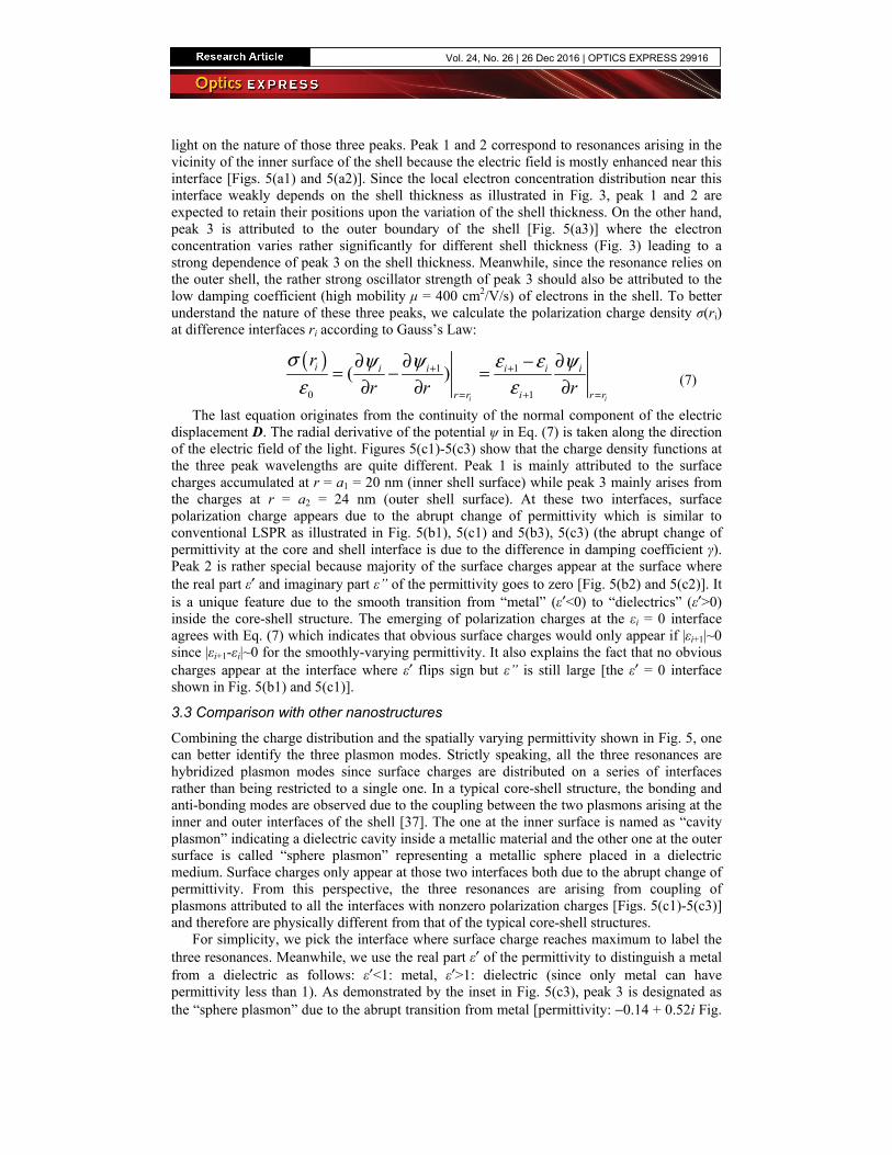
Fig. 6. Comparison of the Quality factors of our core-shell structure with that of other nanostructures from the literatures. The quality factor for Au nanowire(NW) and Au@Ag nanoparticle (NP) are calculated in the Mid infrared region following the result in [4] and [39] respectively. All the other data points are taken directly from the spectrum presented in different papers. 1: Gallium-doped zinc oxide (GZO) nanoparticle [25], 2: Tin-doped indium oxide (ITO) nanoparticle [22], 3: Aluminum-doped zinc oxide (AZO) nanoparticle [25], 4: Phosphorus-doped silicon nanoparticle [40], 5: Phosphorus-doped silicon nanowire [17].
For most applications, peak 3(sphere plasmon) should be adopted because the local field near the particle surface is most significantly enhanced. A more attractive feature is that very strong electric field is confined in the vicinity of the outer boundary [Fig. 5(c1) at 14.1μm]. At the resonance, the maximum field amplitude is about 15E0 (the contour surface is ln|E/E0|) while that of a bare core is about the same as the applied field E0. The confinement of such a strong field near the outer surface makes the core-shell structure very attractive for applications such as nonlinear optics, photothermal therapy etc. Such a field enhancement is attributed to the low damping coefficient (high mobility) of the electrons in the shell. For practical applications, one might also worry about plasmon and phonon coupling at the mid and far infrared waveband. Fortunately, as shown by various literatures, this coupling won’t compromise the strength of the plasmon resonance and in some applications, this coupling can even be exploited to produce phonon-induced transparency [41–44].
As an important figure of merit, quality factor Q is typically used to characterize the strength of a plasmon resonance. We calculated the quality factor Q = ωres/Γ of peak 3 as shown in Fig. 6. ωres is the resonance frequency and Γ is the line width (full width at the half
Vol. 24, No. 26 | 26 Dec 2016 | OPTICS EXPRESS 29917
maximum of the absorption spectrum). For comparison, we also extracted the Q of some experimentally realized structures in the infrared waveband from literatures (scattered points 1 to 5 in Fig. 6). As been illustrated, the predicted quality factor is higher than the ones in the literatures by almost one order of magnitude for all wavelengths.
Meanwhile, we also tried to compare our core-shell structure with Au (the most extensively studied plasmonic material). The LSPR of Au nanostructures typically sits in visible or near infrared waveband. Since the comparison of quality factor is only meaningful at the same resonance frequency, we thus calculated Q for Au nanowire in the Mid-infrared region with the following formula [45]:
res
3res res
2res
/ ( / ).
2 1 ( / )
d dQ ω ωω ε ω ω γ
ε ω γ=
′= =
′′ + (8)
The last expression is obtained using Drude relations defined by Eq. (4). The damping coefficient γ is calculated based on the experimental data in [4]. Due to the drastic decrease of the resonance frequency ωres, the quality factor of gold nanowire appears to be much lower than our structure in the Mid IR waveband (Fig. 6). Similar conclusions can be drawn by applying Eq. (8) for an Au@Ag core-shell nanoparticle [39] and other noble metal nanostructures [46]. It should be noted that such calculations are aiming at comparison of quality factors for structures with different resonance frequencies and do not imply that noble metal nanostructures can be used for mid and far infrared LSPR.
4. Conclusions In conclusion, we proposed a semiconductor core-shell structure and took advantage of diffusive charges to reconcile the conflicts between achieving high carrier density and maintaining high carrier mobility for LSPR. As been theoretically predicted, a triple peak spectrum is expected and the three peaks are designated as “sphere plasmon”, “cavity plasmon” and “gradient plasmon” respectively. The sphere plasmon has a very high quality owing to the high mobility of the diffusive charges and its resonance frequency can be very effectively tuned by shell thickness in the infrared waveband. These results theoretically validates the possibility of arising plasmon resonance with diffusive charges which have the potentials for realizing high quality resonance in mid and far infrared wavebands. The developed theoretical methods also provide a general route for exploring plasmonics of similar structures or systems (e.g. planar PN junction, nanostructures grown epitaxially on a highly-doped substrate etc.).
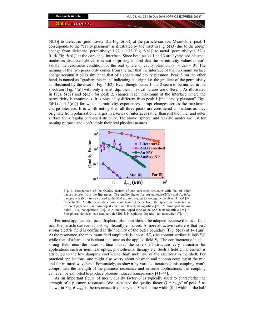
Appendix A: Solve the Poisson’s equation for concentration distribution n(r) Substituting Eqs. (2) and (3) into Eq.(1) yields a differential equation involving only φ and its derivatives with respect to r. This differential equation can be solved as an initial value problem if the potential φ(r) and its derivative dφ(r)/dr at r=0 are known. Based on Gauss’s law, the static electric field Es=-dφ(r)/dr at the particle center must be zero, i.e. dφ(r)/dr=0 at r=0. However, the value of φ(r) at r=0 (φ0) is not defined. φ0 determines the radial concentration distribution of the electrons and its value is regulated by the charge conservation law i.e. total amount of electrons remain unchanged after diffusion. Ignoring the amount of electrons in the shell before diffusion, this condition is written as:
2 2 3
1 00
44 ( ) .
3
ar n r dr a Nπ π= (9)
i.e.
2 2
031 0
3 ( )Ratio 1.
ar n r dr
a N= =
Vol. 24, No. 26 | 26 Dec 2016 | OPTICS EXPRESS 29918
Therefore, by solving Eq. (1) with dφ(r)/dr=0 at r=0 and an adjustable initial condition φ0, one can obtain the correct concentration profile of electrons satisfying Eq. (9). Several iteration steps are shown in Fig. 7.
Fig. 7. Iterations #1, 30, 60, 85 of the simulations. The simulation parameters are as follows: NC is 4 × 1018 cm−3, N0 = 1 × 1020 cm−3
, a1 = 20 nm, a2 = 24nm, T = 300K.
In equilibrium, the drift current density J1=-n(r)μq∇φ caused by the electrostatic force is balanced by the diffusion current density J2=qDdn(r)/dr driven by the concentration gradient i.e. J1+J2=0. This equilibrium condition is equivalent to the force balance described in the main text and is typically used to derive the Einstein relation, which relates the diffusivity D with the carrier mobility μ.
Appendix B: Solve the Laplace equation for absorption cross section.
Due to the gradient of the permittivity i.e. ∇ε(ω,r)≠0, the governing equation for the core-shell structure is written as ∇·[ε0ε(ω,r) ∇ψ]=0, i.e.
2 ( , ).
( , )
r
r
ε ωψ ψε ω
∇∇ = − ⋅∇ (10)
The right hand side of Eq. (10) corresponds to a space polarization charge density proportional to the gradient of the permittivity. Different from the regular electrostatic problem, in which the polarization charge only appears at the interface separating two materials with different permittivity (stepwise change of permittivity), the continuous variation of permittivity results in polarization charges distributed in space. With the proposed multi-shell structure, one can use very fine stepwise changes of permittivity to approximate the smoothly varying permittivity. In this way, the space charges defined on the right hand side of Eq. (10) are approximated by the surface charges on discrete boundaries ri. In each infinitesimal section, ∇ε(ω,r) is zero and Eq. (10) transformed into the Laplace equation ∇2ψ=0. The coefficients αi and βi of the general solution Eq. (5) can be found from boundary conditions. At the boundary of each section, the electrical potential and the normal component of the electric displacement must be continuous. Therefore, the boundary conditions at the boundary r=ri are:
Vol. 24, No. 26 | 26 Dec 2016 | OPTICS EXPRESS 29919
113 3
1
1 11 13 3
= 2 2( ) ( )
i ii i
i i i i
i i i ii i i i
i i
r r
r r
β βα αψ ψ
β βε α ε α
++
+
+ ++ +
− = −= ⋅ ⋅ + = +
D n D n (11)
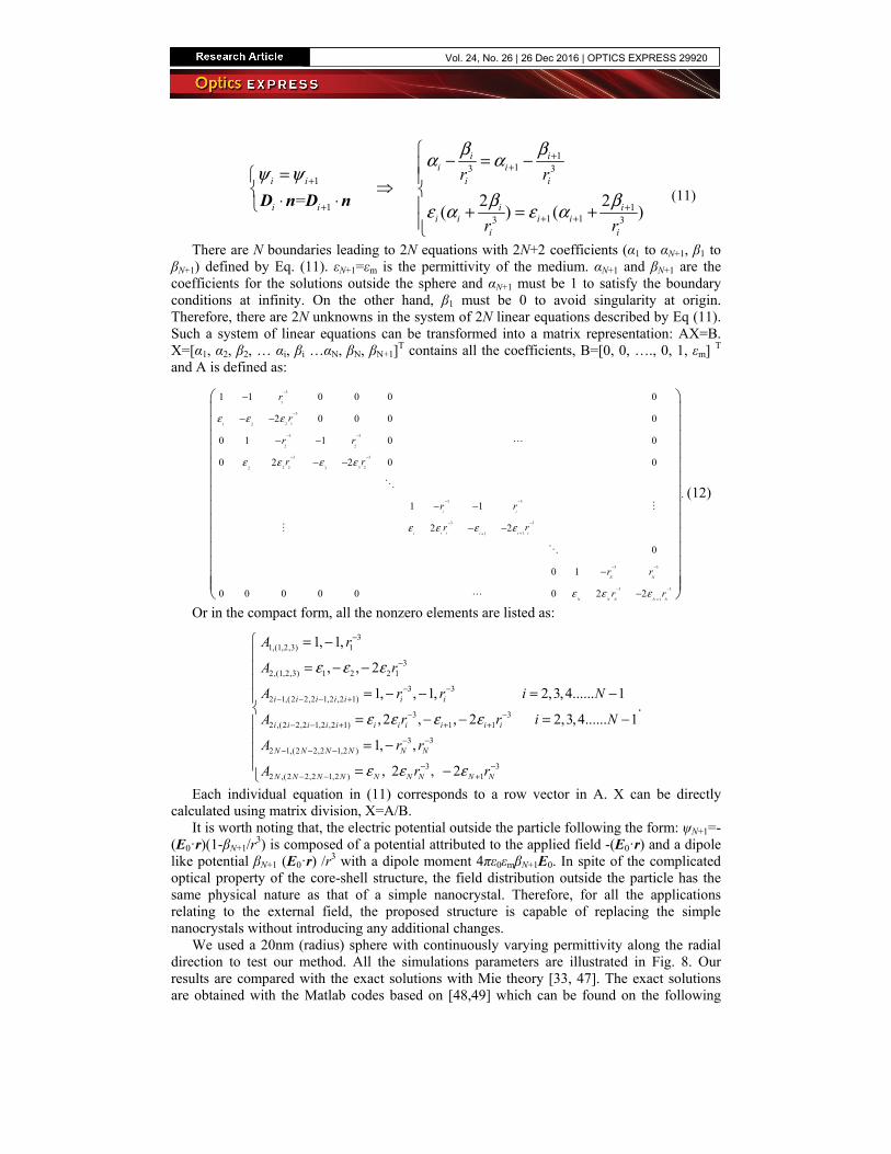
There are N boundaries leading to 2N equations with 2N+2 coefficients (α1 to αN+1, β1 to βN+1) defined by Eq. (11). εN+1=εm is the permittivity of the medium. αN+1 and βN+1 are the coefficients for the solutions outside the sphere and αN+1 must be 1 to satisfy the boundary conditions at infinity. On the other hand, β1 must be 0 to avoid singularity at origin. Therefore, there are 2N unknowns in the system of 2N linear equations described by Eq (11). Such a system of linear equations can be transformed into a matrix representation: AX=B. X=[α1, α2, β2, … αi, βi …αN, βN, βN+1]
T contains all the coefficients, B=[0, 0, …., 0, 1, εm] T and A is defined as:
3
1
3
2 11 2
3 3
2 2
3 3
2 2 3 22 3
3 3
3 3
11
3 3
3 3
1
1 1 0 0 0 0
2 0 0 0 0
0 1 1 0 0
0 2 2 0 0
.1 1
2 2
0
0 1
0 0 0 0 0 0 2 2
−
−
− −
− −
− −
− −
++
− −
− −
+
−
− −
− −
− −
− −
− −
−
−
i i
i i i ii i
N N
N N N N N
r
r
r r
r r
r r
r r
r r
r r
ε ε ε
ε ε ε ε
ε ε ε ε
ε ε ε
(12)
Or in the compact form, all the nonzero elements are listed as:
31,(1,2,3) 1
32,(1,2,3) 1 2 2 1
3 32 1,(2 2,2 1,2 ,2 1)
3 32 ,(2 2,2 1,2 ,2 1) 1 1
1, 1,
, , 2
1, , 1, 2,3,4...... 1
, 2 , , 2 2,3
−
−
− −− − − +
− −− − + + +
= −
= − −
= − − = −
= − − =i i i i i i i
i i i i i i i i i i i
A r
A r
A r r i N
A r r i
ε ε ε
ε ε ε ε
3 3
2 1,(2 2,2 1,2 )
3 32 ,(2 2,2 1,2 ) 1
.,4...... 1
1, ,
, 2 , 2
− −− − −
− −− − +
− = − = −
N N N N N N
N N N N N N N N N
N
A r r
A r rε ε ε
Each individual equation in (11) corresponds to a row vector in A. X can be directly calculated using matrix division, X=A/B.
It is worth noting that, the electric potential outside the particle following the form: ψN+1=-(E0·r)(1-βN+1/r
3) is composed of a potential attributed to the applied field -(E0·r) and a dipole like potential βN+1 (E0·r) /r3 with a dipole moment 4πε0εmβN+1E0. In spite of the complicated optical property of the core-shell structure, the field distribution outside the particle has the same physical nature as that of a simple nanocrystal. Therefore, for all the applications relating to the external field, the proposed structure is capable of replacing the simple nanocrystals without introducing any additional changes.
We used a 20nm (radius) sphere with continuously varying permittivity along the radial direction to test our method. All the simulations parameters are illustrated in Fig. 8. Our results are compared with the exact solutions with Mie theory [33, 47]. The exact solutions are obtained with the Matlab codes based on [48,49] which can be found on the following
Vol. 24, No. 26 | 26 Dec 2016 | OPTICS EXPRESS 29920
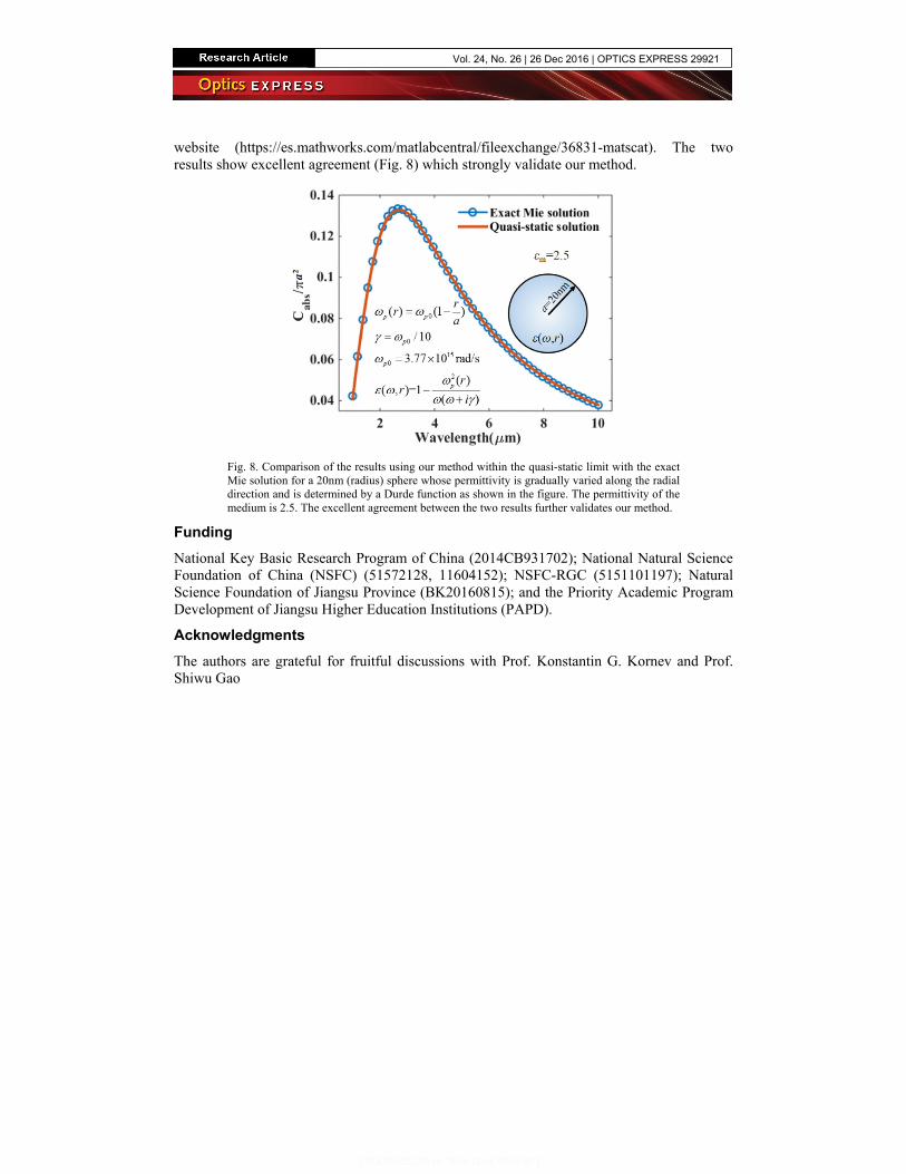
website (https://es.mathworks.com/matlabcentral/fileexchange/36831-matscat). The two results show excellent agreement (Fig. 8) which strongly validate our method.
Fig. 8. Comparison of the results using our method within the quasi-static limit with the exact Mie solution for a 20nm (radius) sphere whose permittivity is gradually varied along the radial direction and is determined by a Durde function as shown in the figure. The permittivity of the medium is 2.5. The excellent agreement between the two results further validates our method.
Funding National Key Basic Research Program of China (2014CB931702); National Natural Science Foundation of China (NSFC) (51572128, 11604152); NSFC-RGC (5151101197); Natural Science Foundation of Jiangsu Province (BK20160815); and the Priority Academic Program Development of Jiangsu Higher Education Institutions (PAPD).
Acknowledgments The authors are grateful for fruitful discussions with Prof. Konstantin G. Kornev and Prof. Shiwu Gao
Vol. 24, No. 26 | 26 Dec 2016 | OPTICS EXPRESS 29921