antennas for light - university of rochester · ptical antennas, analogues of microwave and...
TRANSCRIPT
© 2011 Macmillan Publishers Limited. All rights reserved.
nature photonics | VOL 5 | FEBRUARY 2011 | www.nature.com/naturephotonics 83
Optical antennas, analogues of microwave and radiowave antennas, are a new concept in physical optics1. They are an enabling technology for manipulating and controlling opti-
cal radiation at subwavelength scales2. Optical antennas are the sub-ject of a growing number of scientific studies, and hold promise for enhancing the efficiency of photodetection3,4, light emission5,6, sens-ing7, heat transfer8,9 and spectroscopy10.
Traditionally, the field of optics and photonics deals with the control of propagating optical radiation using elements such as mirrors, lenses, fibres and diffractive elements. On the other hand, in the radiowave and microwave regime, using antennas of vari-ous designs to control electromagnetic fields on the subwavelength scale is a well-established technique. Antennas are pervasive in almost all areas of modern technology, ranging from satellite com-munications to baby phones.
Despite the widespread use of radiowave and microwave anten-nas, the optical analogue has not yet made its debut in technologi-cal applications, primarily because of its small size requirement. The characteristic dimensions of an antenna are of the order of the radia-tion wavelength, and for optical antennas this requires fabrication accuracies down to a few nanometres. However, this length scale has become increasingly accessible as the tools of nanoscience and nanotechnology have improved. Prototype optical antennas have been fabricated by top-down nanofabrication tools such as focused ion beam milling11,12 or electron-beam lithography13,14, and also by bottom-up self-assembly schemes15,16. It is evident that the fabrica-tion of optical antenna structures provides an emerging opportunity for realizing new optoelectronic devices.
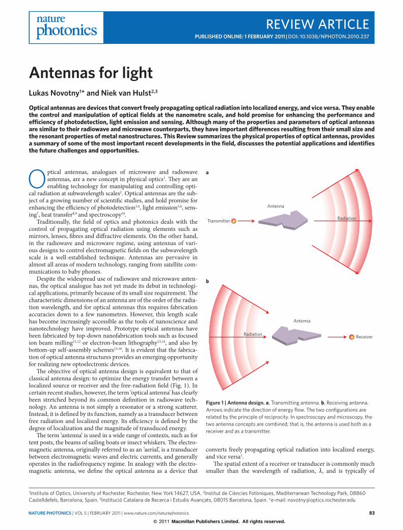
The objective of optical antenna design is equivalent to that of classical antenna design: to optimize the energy transfer between a localized source or receiver and the free-radiation field (Fig. 1). In certain recent studies, however, the term ‘optical antenna’ has clearly been stretched beyond its common definition in radiowave tech-nology. An antenna is not simply a resonator or a strong scatterer. Instead, it is defined by its function, namely as a transducer between free radiation and localized energy. Its efficiency is defined by the degree of localization and the magnitude of transduced energy.
The term ‘antenna’ is used in a wide range of contexts, such as for tent posts, the beams of sailing boats or insect whiskers. The electro-magnetic antenna, originally referred to as an ‘aerial’, is a transducer between electromagnetic waves and electric currents, and generally operates in the radiofrequency regime. In analogy with the electro-magnetic antenna, we define the optical antenna as a device that
antennas for lightLukas novotny1* and niek van hulst2,3
Optical antennas are devices that convert freely propagating optical radiation into localized energy, and vice versa. They enable the control and manipulation of optical fields at the nanometre scale, and hold promise for enhancing the performance and efficiency of photodetection, light emission and sensing. Although many of the properties and parameters of optical antennas are similar to their radiowave and microwave counterparts, they have important differences resulting from their small size and the resonant properties of metal nanostructures. This Review summarizes the physical properties of optical antennas, provides a summary of some of the most important recent developments in the field, discusses the potential applications and identifies the future challenges and opportunities.
converts freely propagating optical radiation into localized energy, and vice versa1.
The spatial extent of a receiver or transducer is commonly much smaller than the wavelength of radiation, λ, and is typically of
1Institute of Optics, University of Rochester, Rochester, New York 14627, USA. 2Institut de Ciències Fotòniques, Mediterranean Technology Park, 08860 Castelldefels, Barcelona, Spain. 3Institució Catalana de Recerca i Estudis Avançats, 08015 Barcelona, Spain. *e-mail: [email protected]
b
Receiver
Transmitter
Antenna
a
Radiation
Antenna
Radiation
Figure 1 | antenna design. a, Transmitting antenna. b, Receiving antenna. Arrows indicate the direction of energy flow. The two configurations are related by the principle of reciprocity. In spectroscopy and microscopy, the two antenna concepts are combined; that is, the antenna is used both as a receiver and as a transmitter.
Review aRticlepubLished onLine: 1 FebruarY 2011 | doi: 10.1038/nphoton.2010.237
© 2011 Macmillan Publishers Limited. All rights reserved.
84 nature photonics | VOL 5 | FEBRUARY 2011 | www.nature.com/naturephotonics
the order of λ/100 (for a cell phone, λ ~ 30 cm). Translating this into the optical frequency regime, we require the dimensions of the receiver or transducer to be ~5 nm. For this length scale the light–matter interaction becomes quantized, and the sources and receivers become quantum objects such as molecules, atoms, ions or quantum dots.
In this Review we attempt to establish a terminology, provide an overview of ongoing research, summarize potential applications and discuss open questions and challenges.
historyThe concept of the optical antenna has its roots in near-field optics17. In 1928, Edward Synge proposed the use of a colloidal gold parti-cle for localizing optical radiation on a sample surface and thereby surpassing the diffraction limit in optical imaging18. Then, in 1985, John Wessel proposed for the first time that a gold particle could function as an antenna19. The first experimental demonstrations of this followed in 1995 by Dieter Pohl and Ulrich Fischer, who used a gold-coated polystyrene particle20. In the following years, optical antennas in the form of sharply pointed metal tips were used in near-field microscopy and spectroscopy10. These experi-ments gave birth to what is today known as ‘tip-enhanced near-field optical microscopy’. It should be noted that antennas were used as whisker (Schottky) diodes for the detection and mixing of infrared radiation in as early as 196821–23. These studies continued,
and since then various infrared antenna geometries have been sys-tematically investigated24,25.
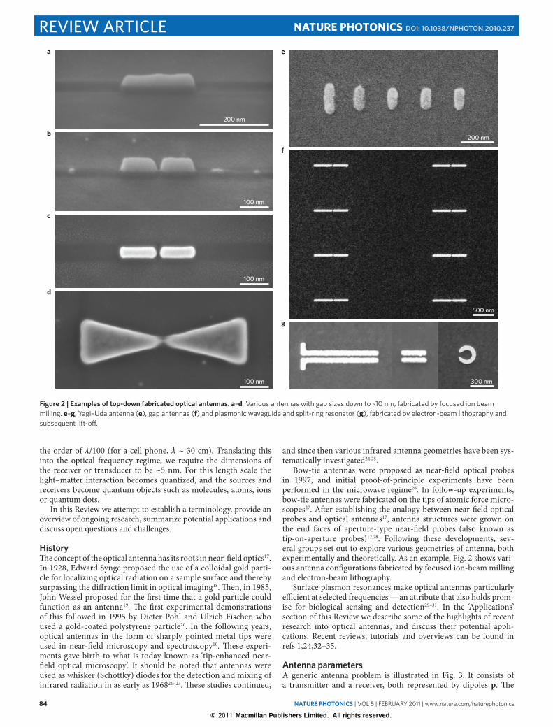
Bow-tie antennas were proposed as near-field optical probes in 1997, and initial proof-of-principle experiments have been performed in the microwave regime26. In follow-up experiments, bow-tie antennas were fabricated on the tips of atomic force micro-scopes27. After establishing the analogy between near-field optical probes and optical antennas17, antenna structures were grown on the end faces of aperture-type near-field probes (also known as tip-on-aperture probes)12,28. Following these developments, sev-eral groups set out to explore various geometries of antenna, both experimentally and theoretically. As an example, Fig. 2 shows vari-ous antenna configurations fabricated by focused ion-beam milling and electron-beam lithography.
Surface plasmon resonances make optical antennas particularly efficient at selected frequencies — an attribute that also holds prom-ise for biological sensing and detection29–31. In the ‘Applications’ section of this Review we describe some of the highlights of recent research into optical antennas, and discuss their potential appli-cations. Recent reviews, tutorials and overviews can be found in refs 1,24,32–35.
antenna parametersA generic antenna problem is illustrated in Fig. 3. It consists of a transmitter and a receiver, both represented by dipoles p. The
200 nm
200 nm
500 nm
300 nm
100 nm
100 nm
100 nm
a e
f
g
b
c
d
Figure 2 | examples of top-down fabricated optical antennas. a–d, Various antennas with gap sizes down to ~10 nm, fabricated by focused ion beam milling. e–g, Yagi–Uda antenna (e), gap antennas (f) and plasmonic waveguide and split-ring resonator (g), fabricated by electron-beam lithography and subsequent lift-off.
Review aRticle NATuRe phOTONics doi: 10.1038/nphoton.2010.237
© 2011 Macmillan Publishers Limited. All rights reserved.
nature photonics | VOL 5 | FEBRUARY 2011 | www.nature.com/naturephotonics 85
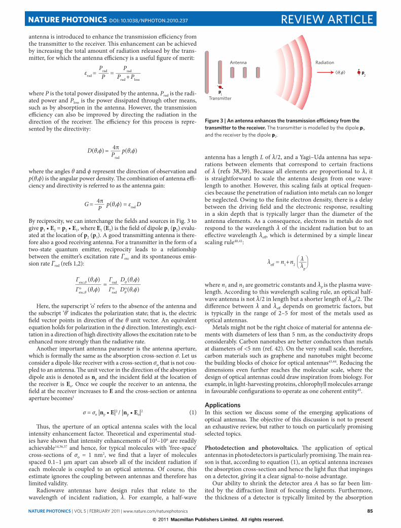
antenna is introduced to enhance the transmission efficiency from the transmitter to the receiver. This enhancement can be achieved by increasing the total amount of radiation released by the trans-mitter, for which the antenna efficiency is a useful figure of merit:
εrad = = Prad
PPrad
Prad + Ploss
where P is the total power dissipated by the antenna, Prad is the radi-ated power and Ploss is the power dissipated through other means, such as by absorption in the antenna. However, the transmission efficiency can also be improved by directing the radiation in the direction of the receiver. The efficiency for this process is repre-sented by the directivity:
D(θ,ϕ) = p(θ,ϕ)4πPrad
where the angles θ and ϕ represent the direction of observation and p(θ,ϕ) is the angular power density. The combination of antenna effi-ciency and directivity is referred to as the antenna gain:
G = p(θ,ϕ) = εrad D4πP
By reciprocity, we can interchange the fields and sources in Fig. 3 to give p1 • E2 = p2 • E1, where E1 (E2) is the field of dipole p1 (p2) evalu-ated at the location of p2 (p1). A good transmitting antenna is there-fore also a good receiving antenna. For a transmitter in the form of a two-state quantum emitter, reciprocity leads to a relationship between the emitter’s excitation rate Γexc and its spontaneous emis-sion rate Γrad (refs 1,2):
= Гexc,θ (θ,ϕ)Гexc,θ (θ,ϕ)
Гrad Dθ (θ,ϕ)Гrad Dθ (θ,ϕ)o o o
Here, the superscript ‘o’ refers to the absence of the antenna and the subscript ‘θ’ indicates the polarization state; that is, the electric field vector points in direction of the θ unit vector. An equivalent equation holds for polarization in the ϕ direction. Interestingly, exci-tation in a direction of high directivity allows the excitation rate to be enhanced more strongly than the radiative rate.
Another important antenna parameter is the antenna aperture, which is formally the same as the absorption cross-section σ. Let us consider a dipole-like receiver with a cross-section σo that is not cou-pled to an antenna. The unit vector in the direction of the absorption dipole axis is denoted as np and the incident field at the location of the receiver is Eo. Once we couple the receiver to an antenna, the field at the receiver increases to E and the cross-section or antenna aperture becomes1
σ = σo |np • E|2 / |np • Eo|2 (1)
Thus, the aperture of an optical antenna scales with the local intensity enhancement factor. Theoretical and experimental stud-ies have shown that intensity enhancements of 104–106 are readily achievable14,36,37 and hence, for typical molecules with ‘free-space’ cross-sections of σo = 1 nm2, we find that a layer of molecules spaced 0.1–1 μm apart can absorb all of the incident radiation if each molecule is coupled to an optical antenna. Of course, this estimate ignores the coupling between antennas and therefore has limited validity.
Radiowave antennas have design rules that relate to the wavelength of incident radiation, λ. For example, a half-wave
antenna has a length L of λ/2, and a Yagi–Uda antenna has sepa-rations between elements that correspond to certain fractions of λ (refs 38,39). Because all elements are proportional to λ, it is straightforward to scale the antenna design from one wave-length to another. However, this scaling fails at optical frequen-cies because the penetration of radiation into metals can no longer be neglected. Owing to the finite electron density, there is a delay between the driving field and the electronic response, resulting in a skin depth that is typically larger than the diameter of the antenna elements. As a consequence, electrons in metals do not respond to the wavelength λ of the incident radiation but to an effective wavelength λeff, which is determined by a simple linear scaling rule40,41:
λeff = n1+ n2 λλp
where n1 and n2 are geometric constants and λp is the plasma wave-length. According to this wavelength scaling rule, an optical half-wave antenna is not λ/2 in length but a shorter length of λeff/2. The difference between λ and λeff depends on geometric factors, but is typically in the range of 2–5 for most of the metals used as optical antennas.
Metals might not be the right choice of material for antenna ele-ments with diameters of less than 5 nm, as the conductivity drops considerably. Carbon nanotubes are better conductors than metals at diameters of <5 nm (ref. 42). On the very small scale, therefore, carbon materials such as graphene and nanotubes might become the building blocks of choice for optical antennas43,44. Reducing the dimensions even further reaches the molecular scale, where the design of optical antennas could draw inspiration from biology. For example, in light-harvesting proteins, chlorophyll molecules arrange in favourable configurations to operate as one coherent entity45.
applicationsIn this section we discuss some of the emerging applications of optical antennas. The objective of this discussion is not to present an exhaustive review, but rather to touch on particularly promising selected topics.
Photodetection and photovoltaics. The application of optical antennas in photodetectors is particularly promising. The main rea-son is that, according to equation (1), an optical antenna increases the absorption cross-section and hence the light flux that impinges on a detector, giving it a clear signal-to-noise advantage.
Our ability to shrink the detector area A has so far been lim-ited by the diffraction limit of focusing elements. Furthermore, the thickness of a detector is typically limited by the absorption
Antenna Radiation
p1
Transmitter
p2
( , )φθ
Figure 3 | an antenna enhances the transmission efficiency from the transmitter to the receiver. The transmitter is modelled by the dipole p1, and the receiver by the dipole p2.
Review aRticleNATuRe phOTONics doi: 10.1038/nphoton.2010.237
© 2011 Macmillan Publishers Limited. All rights reserved.
86 nature photonics | VOL 5 | FEBRUARY 2011 | www.nature.com/naturephotonics
depth of the detector material. Optical antennas can be used in a photodetector to further reduce its critical dimensions and improve performance metrics such as the signal-to-noise ratio, power consumption and speed3,25,29,46. Using antennas reduces the detector area 100-fold, thus gaining at least an order of mag-nitude in sensitivity. The speed of a photodetector depends on the time it takes for photogenerated carriers to traverse the cir-cuit, which scales with the detector size. Similar considerations hold for the power consumption. Because the dark current iD of a photodetector scales with the detector area A we find that both the noise current iN = (2e iD Δf)1/2 and the noise equivalent power NEP = (iN/η) (hν/e) scale with the square root of A. Here, η is the quantum efficiency, ν is the frequency and Δf is the bandwidth. The NEP corresponds to the lowest power a detector can detect with a signal-to-noise ratio of 1. To eliminate the dependence on detector area, one defines the detectivity D* = (AΔf)1/2/NEP, with units of cm Hz1/2 W–1 (known as the Jones). Recent studies have reported values of NEP = 1.53 nW and D* = 2.15 × 10⁶ Jones for antenna-coupled infrared detectors based on metal–oxide–metal diodes47. Current research is aimed at improving these values and extending operation to optical frequencies.
Optical antennas have also been explored for enhancing the efficiency of photovoltaic devices, particularly for solar energy harvesting1,48. The main emphasis is on reducing the photovoltaic layer thickness in thin-film devices to lower the carrier collection length and reduce impurity recombination, while keeping the optical absorption constant48.
Antenna probes for nano-imaging. Over the past decade, optical microscopy has reached the nanoscale through techniques such as stimulated emission depletion (STED) microscopy, photoac-tivatable localization microscopy (PALM) and stochastic optical reconstruction microscopy (STORM)49–53. All of these far-field lens-based methods reveal 20–50 nm features, and rely on the flu-orescence detection of dyes with suitable photodynamic properties for depletion or photoswitching. PALM and STORM in particular are finding rapid acceptance in biological applications.
Optical antennas, when used in scanning probe arrangement, yield a spatial response function on the 10–50 nm scale, independ-ent of the nature and photophysics of the sample; this is in contrast with far-field approaches. Several types of sharp tip were initially exploited to achieve a locally ‘tip-enhanced’ response, with reso-lutions of 10–30 nm achieved in certain cases28,54–56. Dieter Pohl17 was the first to point out the analogy between optical probes and optical antennas, following which scanning antenna probes were steadily investigated. The first of such studies involved attaching colloidal spherical gold particles (~80 nm), tuned to resonance
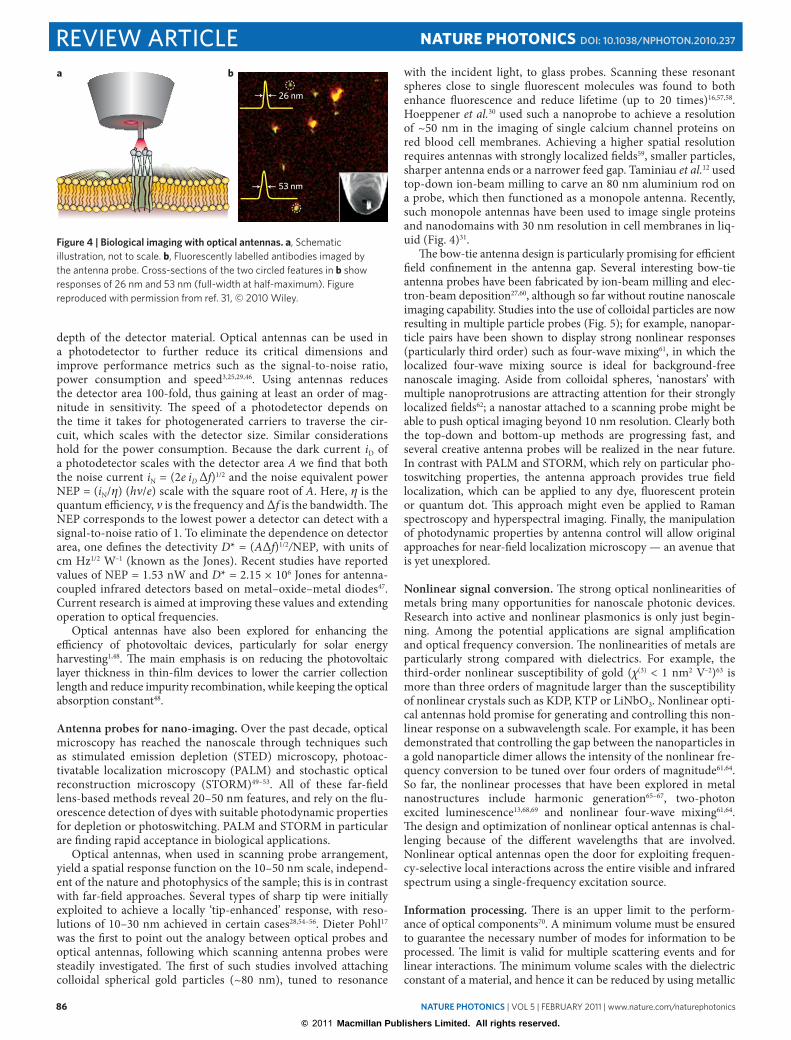
with the incident light, to glass probes. Scanning these resonant spheres close to single fluorescent molecules was found to both enhance fluorescence and reduce lifetime (up to 20 times)16,57,58. Hoeppener et al.30 used such a nanoprobe to achieve a resolution of ~50 nm in the imaging of single calcium channel proteins on red blood cell membranes. Achieving a higher spatial resolution requires antennas with strongly localized fields59, smaller particles, sharper antenna ends or a narrower feed gap. Taminiau et al.12 used top-down ion-beam milling to carve an 80 nm aluminium rod on a probe, which then functioned as a monopole antenna. Recently, such monopole antennas have been used to image single proteins and nanodomains with 30 nm resolution in cell membranes in liq-uid (Fig. 4)31.
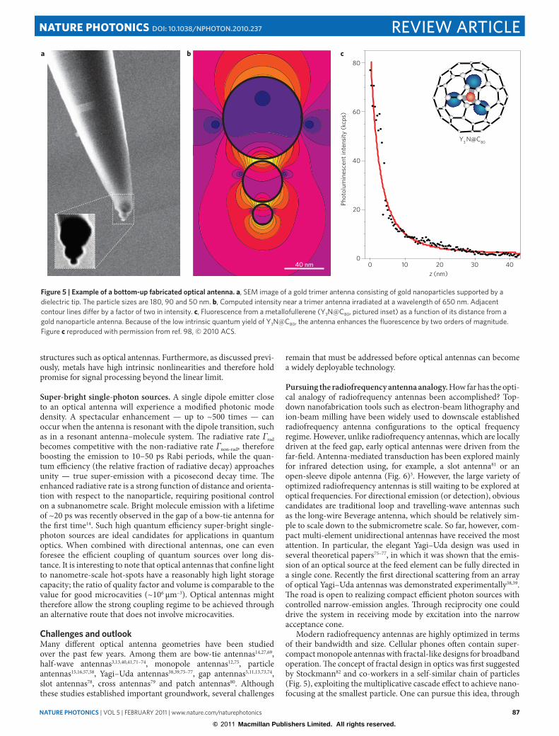
The bow-tie antenna design is particularly promising for efficient field confinement in the antenna gap. Several interesting bow-tie antenna probes have been fabricated by ion-beam milling and elec-tron-beam deposition27,60, although so far without routine nanoscale imaging capability. Studies into the use of colloidal particles are now resulting in multiple particle probes (Fig. 5); for example, nanopar-ticle pairs have been shown to display strong nonlinear responses (particularly third order) such as four-wave mixing61, in which the localized four-wave mixing source is ideal for background-free nanoscale imaging. Aside from colloidal spheres, ‘nanostars’ with multiple nanoprotrusions are attracting attention for their strongly localized fields62; a nanostar attached to a scanning probe might be able to push optical imaging beyond 10 nm resolution. Clearly both the top-down and bottom-up methods are progressing fast, and several creative antenna probes will be realized in the near future. In contrast with PALM and STORM, which rely on particular pho-toswitching properties, the antenna approach provides true field localization, which can be applied to any dye, fluorescent protein or quantum dot. This approach might even be applied to Raman spectroscopy and hyperspectral imaging. Finally, the manipulation of photodynamic properties by antenna control will allow original approaches for near-field localization microscopy — an avenue that is yet unexplored.
Nonlinear signal conversion. The strong optical nonlinearities of metals bring many opportunities for nanoscale photonic devices. Research into active and nonlinear plasmonics is only just begin-ning. Among the potential applications are signal amplification and optical frequency conversion. The nonlinearities of metals are particularly strong compared with dielectrics. For example, the third-order nonlinear susceptibility of gold (χ(3) < 1 nm2 V–2)63 is more than three orders of magnitude larger than the susceptibility of nonlinear crystals such as KDP, KTP or LiNbO3. Nonlinear opti-cal antennas hold promise for generating and controlling this non-linear response on a subwavelength scale. For example, it has been demonstrated that controlling the gap between the nanoparticles in a gold nanoparticle dimer allows the intensity of the nonlinear fre-quency conversion to be tuned over four orders of magnitude61,64. So far, the nonlinear processes that have been explored in metal nanostructures include harmonic generation65–67, two-photon excited luminescence13,68,69 and nonlinear four-wave mixing61,64. The design and optimization of nonlinear optical antennas is chal-lenging because of the different wavelengths that are involved. Nonlinear optical antennas open the door for exploiting frequen-cy-selective local interactions across the entire visible and infrared spectrum using a single-frequency excitation source.
Information processing. There is an upper limit to the perform-ance of optical components70. A minimum volume must be ensured to guarantee the necessary number of modes for information to be processed. The limit is valid for multiple scattering events and for linear interactions. The minimum volume scales with the dielectric constant of a material, and hence it can be reduced by using metallic
26 nm
53 nm
ba
Figure 4 | biological imaging with optical antennas. a, Schematic illustration, not to scale. b, Fluorescently labelled antibodies imaged by the antenna probe. Cross-sections of the two circled features in b show responses of 26 nm and 53 nm (full-width at half-maximum). Figure reproduced with permission from ref. 31, © 2010 Wiley.
Review aRticle NATuRe phOTONics doi: 10.1038/nphoton.2010.237
© 2011 Macmillan Publishers Limited. All rights reserved.
nature photonics | VOL 5 | FEBRUARY 2011 | www.nature.com/naturephotonics 87
structures such as optical antennas. Furthermore, as discussed previ-ously, metals have high intrinsic nonlinearities and therefore hold promise for signal processing beyond the linear limit.
Super-bright single-photon sources. A single dipole emitter close to an optical antenna will experience a modified photonic mode density. A spectacular enhancement — up to ~500 times — can occur when the antenna is resonant with the dipole transition, such as in a resonant antenna–molecule system. The radiative rate Γrad becomes competitive with the non-radiative rate Γnon-rad, therefore boosting the emission to 10–50 ps Rabi periods, while the quan-tum efficiency (the relative fraction of radiative decay) approaches unity — true super-emission with a picosecond decay time. The enhanced radiative rate is a strong function of distance and orienta-tion with respect to the nanoparticle, requiring positional control on a subnanometre scale. Bright molecule emission with a lifetime of ~20 ps was recently observed in the gap of a bow-tie antenna for the first time14. Such high quantum efficiency super-bright single-photon sources are ideal candidates for applications in quantum optics. When combined with directional antennas, one can even foresee the efficient coupling of quantum sources over long dis-tance. It is interesting to note that optical antennas that confine light to nanometre-scale hot-spots have a reasonably high light storage capacity; the ratio of quality factor and volume is comparable to the value for good microcavities (~106 μm–3). Optical antennas might therefore allow the strong coupling regime to be achieved through an alternative route that does not involve microcavities.
challenges and outlookMany different optical antenna geometries have been studied over the past few years. Among them are bow-tie antennas14,27,69, half-wave antennas3,13,40,41,71–74, monopole antennas12,75, particle antennas15,16,57,58, Yagi–Uda antennas38,39,75–77, gap antennas5,11,13,73,74, slot antennas78, cross antennas79 and patch antennas80. Although these studies established important groundwork, several challenges
remain that must be addressed before optical antennas can become a widely deployable technology.
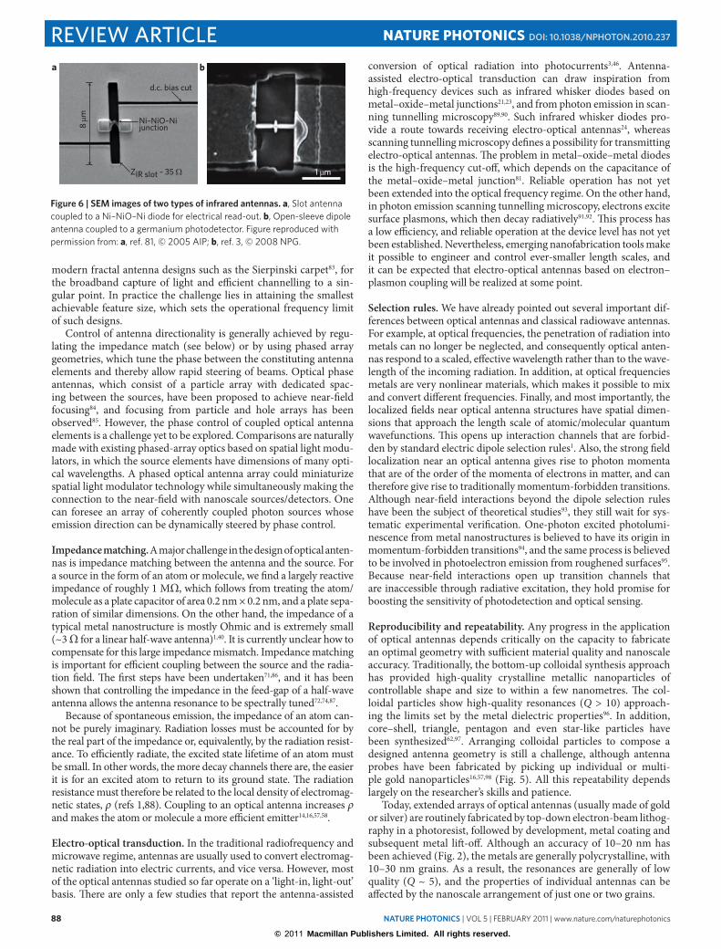
Pursuing the radiofrequency antenna analogy. How far has the opti-cal analogy of radiofrequency antennas been accomplished? Top-down nanofabrication tools such as electron-beam lithography and ion-beam milling have been widely used to downscale established radiofrequency antenna configurations to the optical frequency regime. However, unlike radiofrequency antennas, which are locally driven at the feed gap, early optical antennas were driven from the far-field. Antenna-mediated transduction has been explored mainly for infrared detection using, for example, a slot antenna81 or an open-sleeve dipole antenna (Fig. 6)3. However, the large variety of optimized radiofrequency antennas is still waiting to be explored at optical frequencies. For directional emission (or detection), obvious candidates are traditional loop and travelling-wave antennas such as the long-wire Beverage antenna, which should be relatively sim-ple to scale down to the submicrometre scale. So far, however, com-pact multi-element unidirectional antennas have received the most attention. In particular, the elegant Yagi–Uda design was used in several theoretical papers75–77, in which it was shown that the emis-sion of an optical source at the feed element can be fully directed in a single cone. Recently the first directional scattering from an array of optical Yagi–Uda antennas was demonstrated experimentally38,39. The road is open to realizing compact efficient photon sources with controlled narrow-emission angles. Through reciprocity one could drive the system in receiving mode by excitation into the narrow acceptance cone.
Modern radiofrequency antennas are highly optimized in terms of their bandwidth and size. Cellular phones often contain super-compact monopole antennas with fractal-like designs for broadband operation. The concept of fractal design in optics was first suggested by Stockmann82 and co-workers in a self-similar chain of particles (Fig. 5), exploiting the multiplicative cascade effect to achieve nano-focusing at the smallest particle. One can pursue this idea, through
40
80
60
20
z (nm)
Phot
olum
ines
cent
inte
nsity
(kcp
s)
0 403020100
Y3 N@C80
40 nm
a cb
Figure 5 | example of a bottom-up fabricated optical antenna. a, SEM image of a gold trimer antenna consisting of gold nanoparticles supported by a dielectric tip. The particle sizes are 180, 90 and 50 nm. b, Computed intensity near a trimer antenna irradiated at a wavelength of 650 nm. Adjacent contour lines differ by a factor of two in intensity. c, Fluorescence from a metallofullerene (Y3N@C80, pictured inset) as a function of its distance from a gold nanoparticle antenna. Because of the low intrinsic quantum yield of Y3N@C80, the antenna enhances the fluorescence by two orders of magnitude. Figure c reproduced with permission from ref. 98, © 2010 ACS.
Review aRticleNATuRe phOTONics doi: 10.1038/nphoton.2010.237
© 2011 Macmillan Publishers Limited. All rights reserved.
88 nature photonics | VOL 5 | FEBRUARY 2011 | www.nature.com/naturephotonics
modern fractal antenna designs such as the Sierpinski carpet83, for the broadband capture of light and efficient channelling to a sin-gular point. In practice the challenge lies in attaining the smallest achievable feature size, which sets the operational frequency limit of such designs.
Control of antenna directionality is generally achieved by regu-lating the impedance match (see below) or by using phased array geometries, which tune the phase between the constituting antenna elements and thereby allow rapid steering of beams. Optical phase antennas, which consist of a particle array with dedicated spac-ing between the sources, have been proposed to achieve near-field focusing84, and focusing from particle and hole arrays has been observed85. However, the phase control of coupled optical antenna elements is a challenge yet to be explored. Comparisons are naturally made with existing phased-array optics based on spatial light modu-lators, in which the source elements have dimensions of many opti-cal wavelengths. A phased optical antenna array could miniaturize spatial light modulator technology while simultaneously making the connection to the near-field with nanoscale sources/detectors. One can foresee an array of coherently coupled photon sources whose emission direction can be dynamically steered by phase control.
Impedance matching. A major challenge in the design of optical anten-nas is impedance matching between the antenna and the source. For a source in the form of an atom or molecule, we find a largely reactive impedance of roughly 1 MΩ, which follows from treating the atom/molecule as a plate capacitor of area 0.2 nm × 0.2 nm, and a plate sepa-ration of similar dimensions. On the other hand, the impedance of a typical metal nanostructure is mostly Ohmic and is extremely small (~3 Ω for a linear half-wave antenna)1,40. It is currently unclear how to compensate for this large impedance mismatch. Impedance matching is important for efficient coupling between the source and the radia-tion field. The first steps have been undertaken71,86, and it has been shown that controlling the impedance in the feed-gap of a half-wave antenna allows the antenna resonance to be spectrally tuned72,74,87.
Because of spontaneous emission, the impedance of an atom can-not be purely imaginary. Radiation losses must be accounted for by the real part of the impedance or, equivalently, by the radiation resist-ance. To efficiently radiate, the excited state lifetime of an atom must be small. In other words, the more decay channels there are, the easier it is for an excited atom to return to its ground state. The radiation resistance must therefore be related to the local density of electromag-netic states, ρ (refs 1,88). Coupling to an optical antenna increases ρ and makes the atom or molecule a more efficient emitter14,16,57,58.
Electro-optical transduction. In the traditional radiofrequency and microwave regime, antennas are usually used to convert electromag-netic radiation into electric currents, and vice versa. However, most of the optical antennas studied so far operate on a ‘light-in, light-out’ basis. There are only a few studies that report the antenna-assisted
conversion of optical radiation into photocurrents3,46. Antenna-assisted electro-optical transduction can draw inspiration from high-frequency devices such as infrared whisker diodes based on metal–oxide–metal junctions21,23, and from photon emission in scan-ning tunnelling microscopy89,90. Such infrared whisker diodes pro-vide a route towards receiving electro-optical antennas24, whereas scanning tunnelling microscopy defines a possibility for transmitting electro-optical antennas. The problem in metal–oxide–metal diodes is the high-frequency cut-off, which depends on the capacitance of the metal–oxide–metal junction81. Reliable operation has not yet been extended into the optical frequency regime. On the other hand, in photon emission scanning tunnelling microscopy, electrons excite surface plasmons, which then decay radiatively91,92. This process has a low efficiency, and reliable operation at the device level has not yet been established. Nevertheless, emerging nanofabrication tools make it possible to engineer and control ever-smaller length scales, and it can be expected that electro-optical antennas based on electron–plasmon coupling will be realized at some point.
Selection rules. We have already pointed out several important dif-ferences between optical antennas and classical radiowave antennas. For example, at optical frequencies, the penetration of radiation into metals can no longer be neglected, and consequently optical anten-nas respond to a scaled, effective wavelength rather than to the wave-length of the incoming radiation. In addition, at optical frequencies metals are very nonlinear materials, which makes it possible to mix and convert different frequencies. Finally, and most importantly, the localized fields near optical antenna structures have spatial dimen-sions that approach the length scale of atomic/molecular quantum wavefunctions. This opens up interaction channels that are forbid-den by standard electric dipole selection rules1. Also, the strong field localization near an optical antenna gives rise to photon momenta that are of the order of the momenta of electrons in matter, and can therefore give rise to traditionally momentum-forbidden transitions. Although near-field interactions beyond the dipole selection rules have been the subject of theoretical studies93, they still wait for sys-tematic experimental verification. One-photon excited photolumi-nescence from metal nanostructures is believed to have its origin in momentum-forbidden transitions94, and the same process is believed to be involved in photoelectron emission from roughened surfaces95. Because near-field interactions open up transition channels that are inaccessible through radiative excitation, they hold promise for boosting the sensitivity of photodetection and optical sensing.
Reproducibility and repeatability. Any progress in the application of optical antennas depends critically on the capacity to fabricate an optimal geometry with sufficient material quality and nanoscale accuracy. Traditionally, the bottom-up colloidal synthesis approach has provided high-quality crystalline metallic nanoparticles of controllable shape and size to within a few nanometres. The col-loidal particles show high-quality resonances (Q > 10) approach-ing the limits set by the metal dielectric properties96. In addition, core–shell, triangle, pentagon and even star-like particles have been synthesized62,97. Arranging colloidal particles to compose a designed antenna geometry is still a challenge, although antenna probes have been fabricated by picking up individual or multi-ple gold nanoparticles16,57,98 (Fig. 5). All this repeatability depends largely on the researcher’s skills and patience.
Today, extended arrays of optical antennas (usually made of gold or silver) are routinely fabricated by top-down electron-beam lithog-raphy in a photoresist, followed by development, metal coating and subsequent metal lift-off. Although an accuracy of 10–20 nm has been achieved (Fig. 2), the metals are generally polycrystalline, with 10–30 nm grains. As a result, the resonances are generally of low quality (Q ~ 5), and the properties of individual antennas can be affected by the nanoscale arrangement of just one or two grains.
a b
1 µm
8 µm
d.c. bias cut
Ni–NiO–Nijunction
ZIR slot ~ 35 Ω
Figure 6 | seM images of two types of infrared antennas. a, Slot antenna coupled to a Ni–NiO–Ni diode for electrical read-out. b, Open-sleeve dipole antenna coupled to a germanium photodetector. Figure reproduced with permission from: a, ref. 81, © 2005 AIP; b, ref. 3, © 2008 NPG.
Review aRticle NATuRe phOTONics doi: 10.1038/nphoton.2010.237
© 2011 Macmillan Publishers Limited. All rights reserved.
nature photonics | VOL 5 | FEBRUARY 2011 | www.nature.com/naturephotonics 89
The direct carving of antennas by focused ion beam milling is a good alternative to electron-beam lithography, particularly for more complex three-dimensional structures or dedicated post-processing steps12. Again, reproducibility is a matter of patience. The implanta-tion of gallium ions seems to have an insignificant effect on antenna resonance. Ion-milling could be performed on sheets of crystalline gold or silver, thereby opening the route to high-quality single-crys-talline complex antenna geometries99.
Although techniques in the field of antenna nanofabrication have progressed rapidly, the major hurdle now is how to couple anten-nas to active optical sources such as molecules, quantum dots and nitrogen–vacancy centres. Most work so far has relied on randomly depositing such sources onto an array of antennas, either as a mon-olayer or as a low ‘single-molecule’ concentration. Post-selection can be used to identify ‘hot spots’, and indeed orders of magnitude in antenna enhancement have been observed14, although the exact molecule–antenna arrangement usually remains unknown. Vice versa, colloidal antennas have been spread on pre-patterned sam-ples46. Much more direct control has been achieved by scanning antenna probes in close proximity to molecules or quantum dots, where the relative position and orientation are both fully controlled, giving independent insight on the excitation enhancement and how the emission is modified2,16,57.
For applications, one ideally envisions arrays of antennas, each driven by an optical source (or read-out by an optical detector) at its optimal feed point. Clearly directed nanopositioning of single quantum emitters (detectors) with full control of both location and orientation relative to the antenna remains the challenge for future functional applications.
conclusionsOptical antennas have emerged as the dominant tool for manipu-lating light at the nanometre scale, while also providing optimal control of transduction in the far-field. Current research into optical antennas is being driven in particular by advances in nanofabrica-tion and analogies with radiofrequency antennas. Although many antenna configurations are now being realized at optical frequen-cies, it is interesting to see how antenna concepts such as impedance matching are being redefined for optical sources such as atoms and molecules. Optical antennas connect to quantum systems and pure photon sources, and in doing so involve interesting new physics such as the breaking of selection rules and alternative routes for strong coupling. Concepts of directed emission and directed reception can now be applied to photon emitters. Once the fabrication tech-niques have been mastered, a wide range of applications will emerge, including controlled single-photon sources for quantum informa-tion, light harvesting, energy conversion, efficient biosensors, data storage100,101, nanoscale optical circuitry and optical imaging beyond 10 nm resolution.
references1. Bharadwaj, P., Deutsch, B. & Novotny, L. Optical antennas. Adv. Opt. Photon.
1, 438–483 (2009).2. Taminiau, T. H., Stefani, F. D. & van Hulst, N. F. Enhanced directional
excitation and emission of single emitters by a nano-optical Yagi–Uda antenna. Opt. Express 16, 10858–10866 (2008).
3. Tang, L. et al. Nanometre-scale germanium photodetector enhanced by a near-infrared dipole antenna. Nature Photon. 2, 226–229 (2008).
4. Cao, L., Park, J.-S., Fan, P., Clemens, B. & Brongersma, M. L. Resonant Germanium nanoantenna photodetectors. Nano Lett. 10, 1229–1233 (2010).
5. Cubukcu, E., Kort, E. A., Crozier, K. B. & Capasso, F. Plasmonic laser antenna. Appl. Phys. Lett. 89, 093120 (2006).
6. Pillai, S., Catchpole, K., Trupke, T. & Green, M. Surface plasmon enhanced silicon solar cells. J. Appl. Phys. 101, 093105 (2007).
7. Anker, J. N. et al. Biosensing with plasmonic nanosensors. Nature Mater. 7, 442–453 (2008).
8. DeWilde, Y. et al. Thermal radiation scanning tunnelling microscopy. Nature 444, 740 (2006).
9. Schuller, J. A., Taubner, T. & Brongersma, M. L. Optical antenna thermal emitters. Nature Photon. 3, 658–661 (2009).
10. Novotny, L. & Stranick, S. J. Near-field optical microscopy and spectroscopy with pointed probes. Ann. Rev. Phys. Chem. 57, 303–331 (2006).
11. Muehlschlegel, P., Eisler, H.-J., Martin, O. J. F., Hecht, B. & Pohl, D. W. Resonant optical antennas. Science 308, 1607–1609 (2005).
12. Taminiau, T. H. et al. Resonance of an optical monopole antenna probed by single molecule fluorescence. Nano Lett. 7, 28–33 (2007).
13. Ghenuche, P., Cherukulappurath, S., Taminiau, T. H., van Hulst, N. F. & Quidant, R. Spectroscopic mode mapping of resonant plasmon nanoantennas. Phys. Rev. Lett. 101, 116805 (2008).
14. Kinkhabwala, A. et al. Large single-molecule fluorescence enhancements produced by a bowtie nanoantenna. Nature Photon. 3, 654–657 (2009).
15. Kalkbrenner, T. et al. Optical microscopy via spectral modifications of a nanoantenna. Phys. Rev. Lett. 95, 200801 (2005).
16. Anger, P., Bharadwaj, P. & Novotny, L. Enhancement and quenching of single molecule fluorescence. Phys. Rev. Lett. 96, 113002 (2006).
17. Pohl, D. W. Near-field optics seen as an antenna problem in Near-field Optics, Principles and Applications (eds Zhu, X. & Ohtsu, M.) 9–21 (World Scientific, 2000).
18. Novotny, L. Effective wavelength scaling for optical antennas. Phys. Rev. Lett. 98, 266802 (2007).
19. Wessel, J. Surface-enhanced optical microscopy. J. Opt. Soc. Am. B 2, 1538–1540 (1985).
20. Fischer, U. C. & Pohl, D. W. Observation on single-particle plasmons by near-field optical microscopy. Phys. Rev. Lett. 62, 458–461 (1989).
21. Hocker, L. O., Sokoloff, D. R., V. Daneu, A. S. & Javan, A. Frequency mixing in the infrared and far-infrared using metal-to-metal point contact diode. Appl. Phys. Lett. 12, 401–402 (1968).
22. Fetterman, H. R., Clifton, B. J., Tannenwald, P. E. & Parker, C. D. Submillimeter detection and mixing using Schottky diodes. Appl. Phys. Lett. 24, 70–72 (1974).
23. Fetterman, H. R. et al. Far-IR heterodyne radiometric measurements with quasioptical Schottky diode mixers. Appl. Phys. Lett. 33, 151–153 (1978).
24. Alda, J., Rico-Garcia, J., Lopez-Alonso, J. & Boreman, G. Optical antennas for nano-photonic applications. Nanotechnology 16, S230–S234 (2005).
25. Gonzalez, F. & Boreman, G. Comparison of dipole, bowtie, spiral and log-periodic IR antennas. Infrared Phys. Technol. 146, 418–428 (2004).
26. Grober, R. D., Schoelkopf, R. J. & Prober, D. E. Optical antenna: towards a unity efficiency near-field optical probe. Appl. Phys. Lett. 70, 1354–1356 (1997).
27. Farahani, J. N., Pohl, D. W., Eisler, H.-J. & Hecht, B. Single quantum dot coupled to a scanning optical antenna: A tunable superemitter. Phys. Rev. Lett. 95, 017402 (2005).
28. Frey, H. G., Witt, S., Felderer, K. & Guckenberger, R. High-resolution imaging of single fluorescent molecules with the optical near-field of a metal tip. Phys. Rev. Lett. 93, 200801 (2004).
29. Schuller, J. A. et al. Plasmonics for extreme light concentration and manipulation. Nature Mater. 9, 193–204 (2010).
30. Hoeppener, C. & Novotny, L. Antenna-based optical imaging of single Ca2+ transmembrane proteins in liquids. Nano Lett. 8, 642–646 (2008).
31. van Zanten, T. S., Lopez-Busquets, M. J. & Garcia-Parajo, M. F. Imaging individual proteins and nanodomains on intact cell membranes with a probe-based optical antenna. Small 6, 270–275 (2010).
32. Hecht, B., Muehlschlegel, P., Farahani, J., Eisler, H.-J. & Pohl, D. W. Resonant optical antennas and single emitters in Tip Enhancement (eds Kawata, S. & Shalaev, V. M.) 275–307 (Elsevier, 2007).
33. Gevaux, D. Nano-antenna picks up green light. Nature Photon. 1, 90 (2007).34. Novotny, L. Optical antennas tuned to pitch. Nature 455, 879–880 (2008).35. Greffet, J.-J. Nanoantennas for light emission. Science 308, 1561–1563 (2005).36. Novotny, L., Bian, R. X. & Xie, X. S. Theory of nanometric optical tweezers.
Phys. Rev. Lett. 79, 645–648 (1997).37. Crozier, K. B., Sundaramurthy, A., Kino, G. S. & Quate, C. F. Optical antennas:
Resonators for local field enhancement. J. Appl. Phys. 94, 4632–4642 (2003).38. Curto, A. G. et al. Unidirectional emission of a quantum dot coupled to a
nanoantenna. Science 329, 930–933 (2010).39. Kosako, T., Kadoya, Y. & Hofmann, H. F. Directional control of light by a
nano-optical Yagi–Uda antenna. Nature Photon. 4, 312–315 (2010).40. Novotny, L. The history of near-field optics. Prog. Opt. 50, 137–180 (2007).41. Bryant, G. W., de Abajo, F. J. G. & Aizpurua, J. Mapping the plasmon
resonances of metallic nanoantennas. Nano Lett. 8, 631–636 (2008).42. Sfeir, M. Y. et al. Optical spectroscopy of individual single-walled carbon
nanotubes of defined chiral structure. Science 312, 554–556 (2006).43. Burke, P. J., Li, S. & Yu, Z. Quantitative theory of nanowire and nanotube
antenna performance. IEEE Trans. Nanotech. 5, 314–334 (2006).44. Hao, J. & Hanson, G. W. Infrared and optical properties of carbon nanotube
dipole antennas. IEEE T. Nanotechnol. 5, 766–775 (2006).
Review aRticleNATuRe phOTONics doi: 10.1038/nphoton.2010.237

© 2011 Macmillan Publishers Limited. All rights reserved.
90 nature photonics | VOL 5 | FEBRUARY 2011 | www.nature.com/naturephotonics
45. Blankenship, R., Madigan, M. T. & Bauer, C. E. (eds) Anoxygenic Photosynthetic Bacteria (Kluwer, 1995).
46. Falk, A. L. et al. Near-field electrical detection of optical and single-plasmon sources. Nature Phys. 5, 475–479 (2009).
47. Bean, J. A., Tiwari, B., Bernstein, G. H., Fay, P. & Porod, W. Thermal infrared detection using dipole antenna-coupled metal-oxide-metal diodes. J. Vac. Sci. Technnol. B 27, 11–14 (2009).
48. Atwater, H. A. & Polman, A. Plasmonics for improved photovoltaic devices. Nature Mater. 9, 205–213 (2010).
49. Hell, S. W. & Wichmann, J. Breaking the diffraction resolution limit by stimulated emission: Stimulated-emission-depletion fluorescence microscopy. Opt. Lett. 19, 780–782 (1994).
50. Westphal, V. & Hell, S. W. Nanoscale resolution in the focal plane of an optical microscope. Phys. Rev. Lett. 94, 143903 (2005).
51. Betzig, E. Proposed method for molecular optical imaging. Opt. Lett. 20, 237–239 (1995).
52. Betzig, E. et al. Imaging intracellular fluorescent proteins at nanometer resolution. Science 313, 1642–1645 (2006).
53. Rust, M., Bates, M. & Zhuang, X. Sub-diffraction limit imaging by stochastic optical reconstruction microscopy (storm). Nat. Methods 3, 793–796 (2006).
54. Sanchez, E. J., Novotny, L. & Xie, X. S. Near-field fluorescence microscopy based on two-photon excitation with metal tips. Phys. Rev. Lett. 82, 4014–4017 (1999).
55. Gerton, J. M., Wade, L. A., Lessard, G. A., Ma, Z. & Quake, S. R. Tip-enhanced fluorescence microscopy at 10 nanometer resolution. Phys. Rev. Lett. 93, 180801 (2004).
56. Hartschuh, A., Sanchez, E., Xie, X. & Novotny, L. High-resolution near-field Raman microscopy of single-walled carbon nanotubes. Phys. Rev. Lett. 90, 095503 (2003).
57. Kuehn, S., Hakanson, U., Rogobete, L. & Sandoghdar, V. Enhancement of single-molecule fluorescence using a gold nanoparticle as an optical nanoantenna. Phys. Rev. Lett. 97, 017402 (2006).
58. Bharadwaj, P. & Novotny, L. Spectral dependence of single molecule fluorescence enhancement. Opt. Express 15, 14266–14274 (2007).
59. Garcia-Parajo, M. F. Optical antennas focus in on biology. Nature Photon. 2, 201–203 (2008).
60. Weber-Bargioni, A. et al. Functional plasmonic antenna scanning probes fabricated by induced-deposition mask lithography. Nanotechnology 21, 065306 (2010).
61. Palomba, S. & Novotny, L. Near-field imaging with a localized nonlinear light source. Nano Lett. 9, 3801–1804 (2009).
62. Rodriguez-Lorenzo, L. et al. Zeptomol detection through controlled ultrasensitive surface enhanced Raman scattering. J. Am. Chem. Soc. 131, 4616–4618 (2009).
63. Renger, J., Quidant, R., Hulst, N. V. & Novotny, L. Surface enhanced nonlinear four-wave mixing. Phys. Rev. Lett. 104, 046803 (2010).
64. Danckwerts, M. & Novotny, L. Optical frequency mixing at coupled gold nanoparticles. Phys. Rev. Lett. 98, 026104 (2007).
65. Bouhelier, A., Beversluis, M., Hartschuh, A. & Novotny, L. Near-field second-harmonic generation induced by local field enhancement. Phys. Rev. Lett. 90, 013903 (2003).
66. Lippitz, M., van Dijk, M. A. & Orrit, M. Third-harmonic generation from single gold nanoparticles. Nano Lett. 5, 799–802 (2005).
67. Kim, S. et al. High-harmonic generation by resonant plasmon field enhancement. Nature 453, 757–760 (2008).
68. Bouhelier, A., Beversluis, M. R. & Novotny, L. Characterization of nanoplasmonic structures by locally excited photoluminescence. Appl. Phys. Lett. 83, 5041–5043 (2003).
69. Schuck, P., Fromm, D. P., Sundaramurthy, A., Kino, G. S. & Moerner, W. E. Improving the mismatch between light and nanoscale objects with gold bowtie nanoantennas. Phys. Rev. Lett. 94, 017402 (2005).
70. Miller, D. A. B. Fundamental limit for optical components. J. Opt. Soc. Am. B 24, A1–A18 (2007).
71. Alu, A. & Engheta, N. Input impedance, nanocircuit loading, and radiation tuning of optical nanoantennas. Phys. Rev. Lett. 101, 043901 (2008).
72. Alu, A. & Engheta, N. Hertzian plasmonic nanodimer as an efficient optical nanoantenna. Phys. Rev. B 78, 195111 (2008).
73. Olmon, R. L., Krenz, P. M., Jones, A. C., Boreman, G. D. & Raschke, M. B. Near-field imaging of optical antenna modes in the mid-infrared. Opt. Express 16, 20295–20305 (2008).
74. Schnell, M. et al. Controlling the near-field oscillations of loaded plasmonic nanoantennas. Nature Photon. 3, 287–291 (2009).
75. Taminiau, T. H., Stefani, F. D., Segerink, F. B. & van Hulst, N. F. Optical antennas direct single-molecule emission. Nature Photon. 2, 234–237 (2008).
76. Hofmann, H. F., Kosako, T. & Kadoya, Y. Design parameters for a nano-optical Yagi–Uda antenna. New J. Phys. 9, 217–217 (2007).
77. Li, J., Salandrino, A. & Engheta, N. Shaping light beams in the nanometer scale: A Yagi–Uda nanoantenna in the optical domain. Phys. Rev. B 76, 245403 (2007).
78. Guo, H. et al. Optical resonances of bowtie slot antennas and their geometry and material dependence. Opt. Express 16, 7756–7766 (2008).
79. Biagioni, P., Huang, J. S., Duò, L., Finazzi, M. & Hecht, B. Cross resonant optical antenna. Phys. Rev. Lett. 102, 256801 (2009).
80. Esteban, R., Teperik, T. V. & Greffet, J.-J. Optical patch antennas for single photon emission using surface plasmon resonances. Phys. Rev. Lett. 104, 026802 (2010).
81. Abdel-Rahman, M. R., Monacelli, B., Weeks, A. R., Zummo, G. & Boreman, G. D. Design, fabrication and characterization of antenna-coupled metal-oxide-metal diodes for dual-band detection. Opt. Eng. 44, 066401 (2005).
82. Li, K., Stockman, M. I. & Bergman, D. J. Self-similar chain of metal nanospheres as an efficient nanolens. Phys. Rev. Lett. 91, 227402 (2003).
83. Puente-Biliarda, C., Romeu, J., Pous, R. & Cardama, A. On the behavior of the sierpinski multiband fractal antenna. IEEE T. Antenn. Propag. 46, 517–524 (1998).
84. Curto, A. G., Manjavacas, A. & de Abajo, F. J. G. Near-field focusing with optical phase antennas. Opt. Express 17, 17801–17811 (2009).
85. Huang, C. et al. Gain, detuning, and radiation patterns of nanoparticles optical antennas. Phys. Rev. B 88, 155407 (2008).
86. Huang, J.-S., Feichtner, T., Biagioni, P. & Hecht, B. Impedance matching and emission properties of nanoantennas in an optical nanocircuit. Nano Lett. 9, 1897–1902 (2009).
87. Berthelot, J. et al. Tuning of an optical dimer nanoantenna by electrically controlling its load impedance. Nano Lett. 9, 3914–3921 (2009).
88. Greffet, J.-J., Laroche, M. & Marquier, F. Impedance of a nanoantenna and a single quantum emitter. Phys. Rev. Lett. 105, 117701 (2010).
89. Gimzewski, J. K., Reihl, B., Coombs, J. H. & Schlittler, R. R. Photon emission with the scanning tunneling microscope. Z. Phys. B 72, 497–501 (1988).
90. Schull, G., Nel, N., Johanson, P. & Berndt, R. Electron–plasmon and electron–electron interactions at a single atom contact. Phys. Rev. Lett. 102, 057401 (2009).
91. Johansson, P., Monreal, R. & Apell, P. Theory for light emission from a scanning tunneling microscope. Phys. Rev. B 42, 9210–9213 (1990).
92. Persson, B. N. J. & Baratoff, A. Theory of photon emission in electron tunneling to metallic particles. Phys. Rev. B 68, 3224–3227 (1992).
93. Zurita-Sanchez, J. R. & Novotny, L. Multipolar interband absorption in a semiconductor quantum dot. I. Electric quadrupole enhancement. J. Opt. Soc. Am. B 19, 1355–1362 (2002).
94. Beversluis, M. R., Bouhelier, A. & Novotny, L. Continuum generation from single gold nanostructures through near-field mediated intraband transitions. Phys. Rev. B 68, 115433 (2003).
95. Shalaev, V. M., Douketis, C., Haslett, T., Stuckless, T. & Moskovits, M. Two-photon electron emission from smooth and rough metal films in the threshold region. Phys. Rev. B 53, 11193–11206 (1996).
96. Ditlbacher, H. et al. Silver nanowires as surface plasmon resonators. Phys. Rev. Lett. 95, 257403 (2005).
97. Averitt, R. D., Sarkar, D. & Halas, N. J. Plasmon resonance shifts of Au-coated Au2S nanoshells: Insight into multicomponent nanoparticle growth. Phys. Rev. Lett. 78, 4217–4220 (1997).
98. Bharadwaj, P. & Novotny, L. Plasmon-enhanced photoemission from a single Y3N@C80 fullerene. J. Phys. Chem. C 114, 7444–7447 (2010).
99. Huang, J.-S. et al. Atomically flat single-crystalline gold nanostructures for plasmonic nanocircuitry. Nature Comm. 1, 150 (2010).
100. Challener, W. A. et al. Heat-assisted magnetic recording by a near-field transducer with efficient optical energy transfer. Nature Photon. 3, 220–224 (2009).
101. Stipe, B. C. et al. Magnetic recording at 1.5 Pb m−2 using an integrated plasmonic antenna. Nature Photon. 4, 484–488 (2010).
acknowledgementsN.L. and N.v.H. thank C. Hoeppener and P. Bharadwaj for providing the particle trimer probe shown in Fig. 5a. They also thank T. Taminiau for valuable discussions. N.L. and N.v.H. thank M. Castro-Lopez, G. Volpe, L. Neumann, A. Curto, M. Kuttge and R. Quidant for providing several top-down fabricated antennas. L.N. acknowledges financial support from the US Department of Energy (DE-FG02-01ER15204) and the National Science Foundation (ECCS- 0918416 and ECCS-0651079). N.v.H. thanks the Spanish Ministry of Science and Innovation (CSD2007-046-NanoLight.es and FIS2009-08203), the Fundacio Cellex Barcelona and the European Research Council (AdvGrant ERC247330) for financial support.
additional informationThe authors declare no competing financial interests.
Review aRticle NATuRe phOTONics doi: 10.1038/nphoton.2010.237