“design of combinational logic” · binary adder (ic 7483) 4. bcd adder 5. look ahead carry...
TRANSCRIPT
Pune Vidyarthi Griha’s
COLLEGE OF ENGINEERING, NASHIK – 3.
“Design of Combinational Logic”
By
Prof. Anand N. Gharu (Assistant Professor)
PVGCOE Computer Dept.
30th June 2017 .
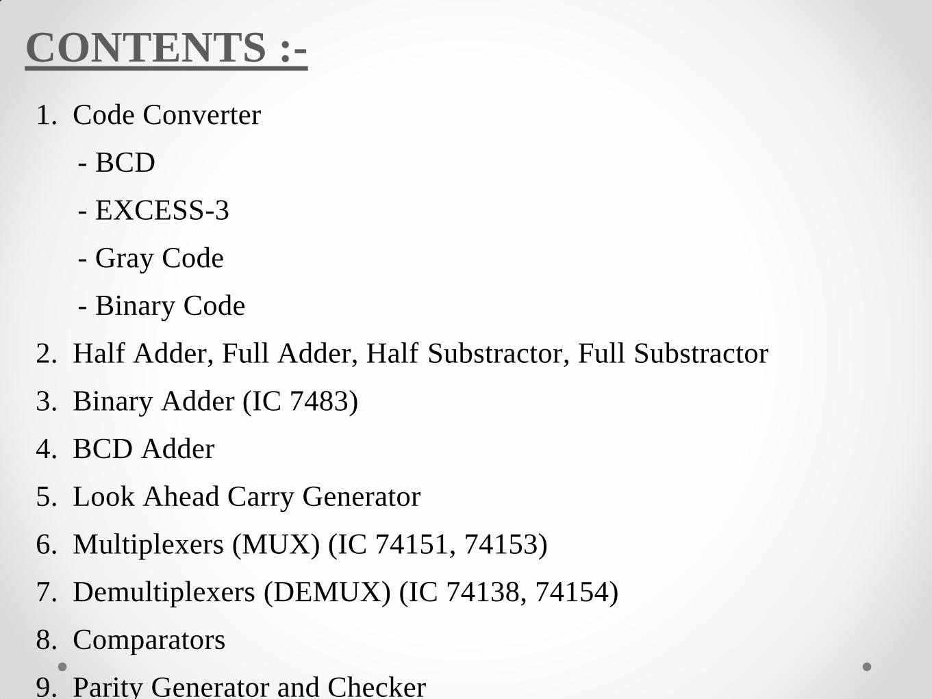
CONTENTS :-
1. Code Converter
- BCD
- EXCESS-3
- Gray Code
- Binary Code
2. Half Adder, Full Adder, Half Substractor, Full Substractor
3. Binary Adder (IC 7483)
4. BCD Adder
5. Look Ahead Carry Generator
6. Multiplexers (MUX) (IC 74151, 74153)
7. Demultiplexers (DEMUX) (IC 74138, 74154)
8. Comparators
9. Parity Generator and Checker
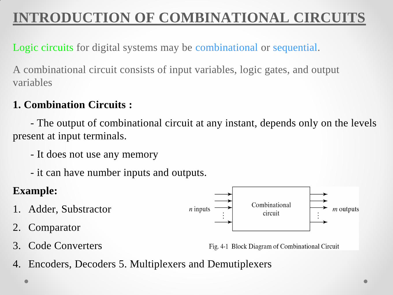
INTRODUCTION OF COMBINATIONAL CIRCUITS
Logic circuits for digital systems may be combinational or sequential.
A combinational circuit consists of input variables, logic gates, and output
variables
1. Combination Circuits :
- The output of combinational circuit at any instant, depends only on the levels
present at input terminals.
- It does not use any memory
- it can have number inputs and outputs.
Example:
1. Adder, Substractor
2. Comparator
3. Code Converters
4. Encoders, Decoders 5. Multiplexers and Demutiplexers
4
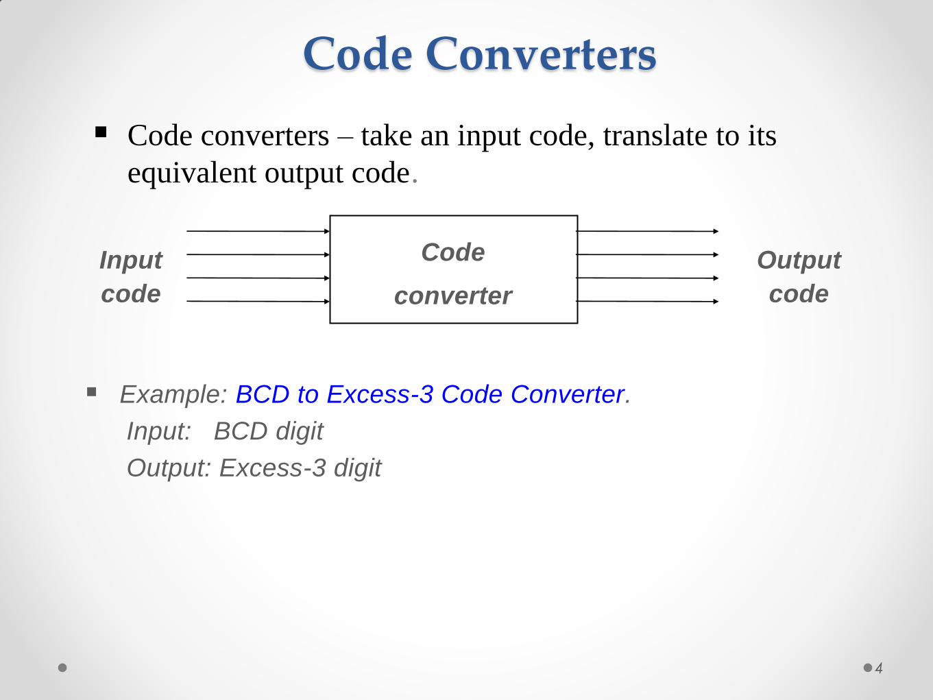
Code Converters
Code converters – take an input code, translate to its
equivalent output code.
Code
converter
Input
code
Output
code
Example: BCD to Excess-3 Code Converter.
Input: BCD digit
Output: Excess-3 digit
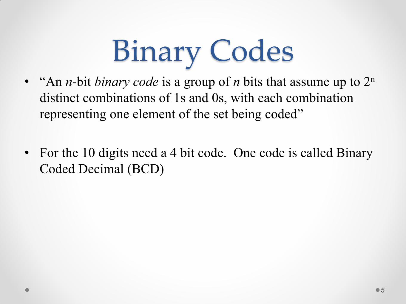
Binary Codes • “An n-bit binary code is a group of n bits that assume up to 2n
distinct combinations of 1s and 0s, with each combination
representing one element of the set being coded”
• For the 10 digits need a 4 bit code. One code is called Binary
Coded Decimal (BCD)
5
Binary Coded Decimal
ex1: dec-to-BCD
(a) 35
(b) 98
(c) 170
(d) 2469
ex2: BCD-to-dec
(a) 10000110
(b) 001101010001
(c) 1001010001110000
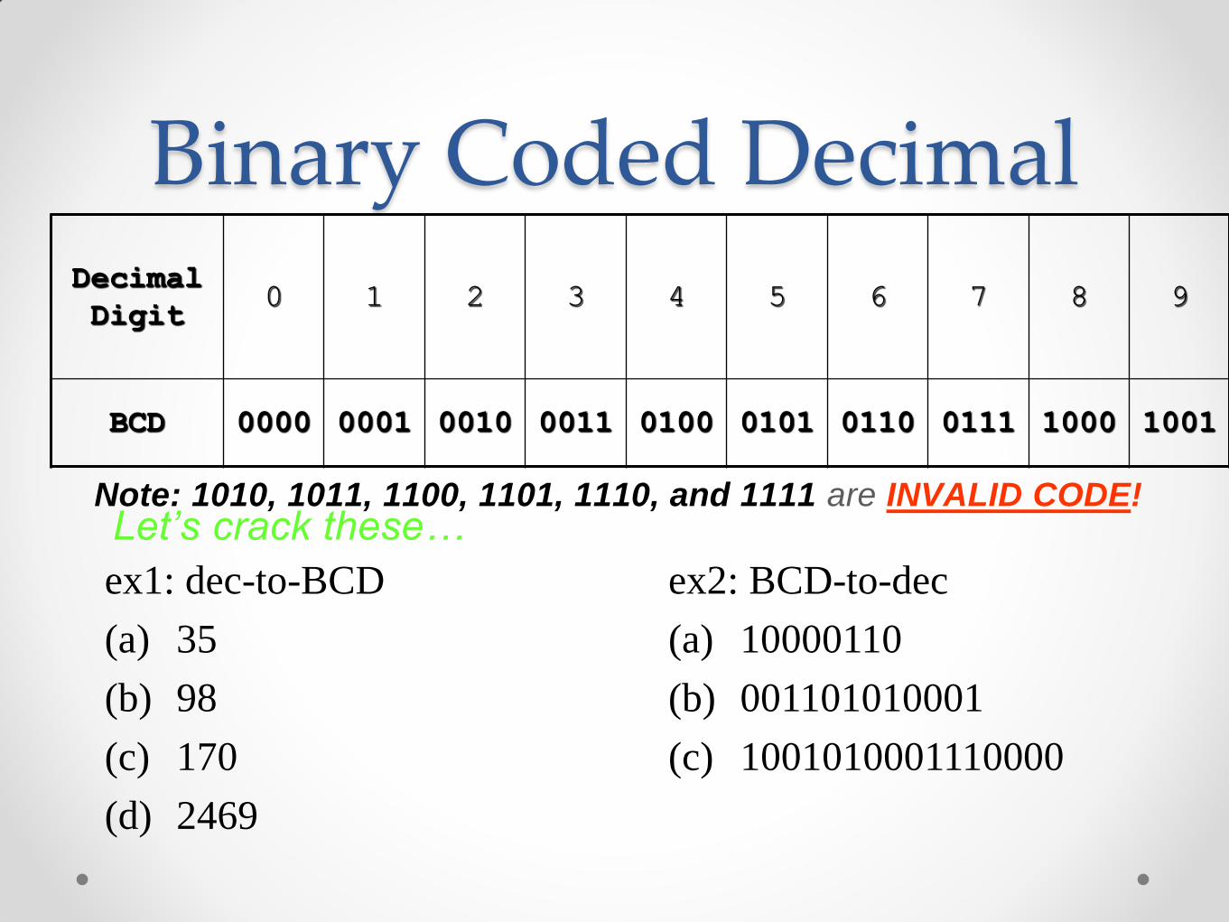
Decimal
Digit 0 1 2 3 4 5 6 7 8 9
BCD 0000 0001 0010 0011 0100 0101 0110 0111 1000 1001
Let’s crack these… Note: 1010, 1011, 1100, 1101, 1110, and 1111 are INVALID CODE!
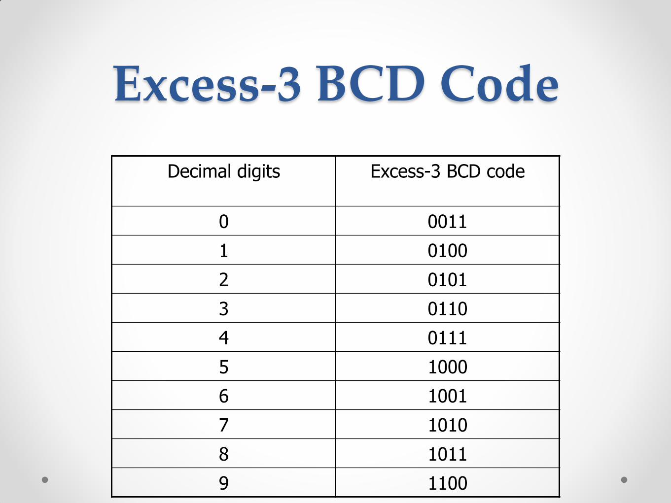
Excess-3 BCD Code
Decimal digits Excess-3 BCD code
0 0011
1 0100
2 0101
3 0110
4 0111
5 1000
6 1001
7 1010
8 1011
9 1100
8/29/2017 Amit Nevase 8
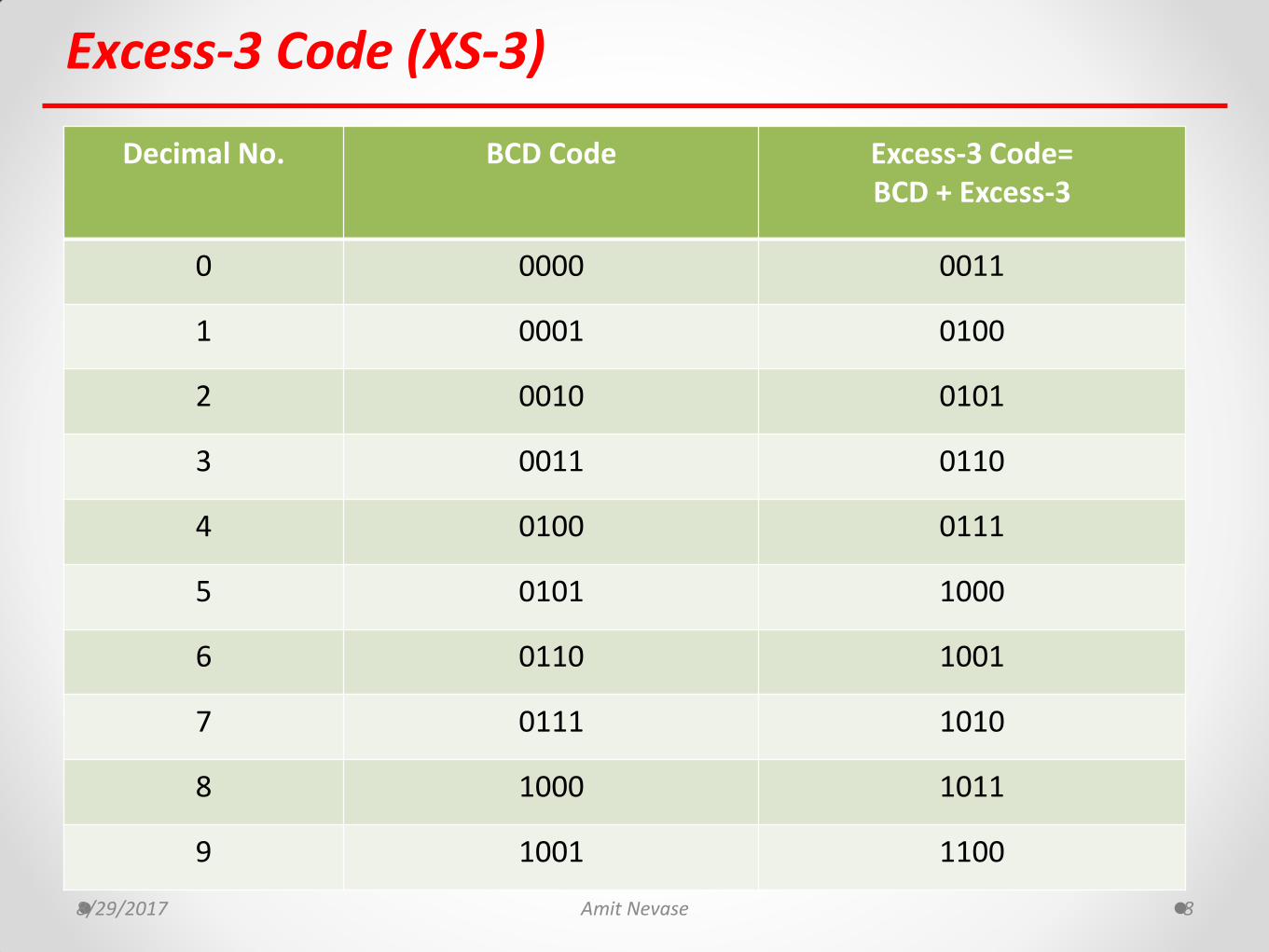
Excess-3 Code (XS-3)
Decimal No. BCD Code Excess-3 Code=
BCD + Excess-3
0 0000 0011
1 0001 0100
2 0010 0101
3 0011 0110
4 0100 0111
5 0101 1000
6 0110 1001
7 0111 1010
8 1000 1011
9 1001 1100
8/29/2017 Amit Nevase 9
Excess-3 Code (XS-3)
Example 1: Obtain Xs-3 Code for 428 Decimal
8/29/2017 Amit Nevase 10
Excess-3 Code (XS-3)
Example 1: Obtain Xs-3 Code for 428 Decimal
4 2 8
0100 0010 1000
+ 0011 0011 0011
0111 0101 1011
8/29/2017 Amit Nevase 11
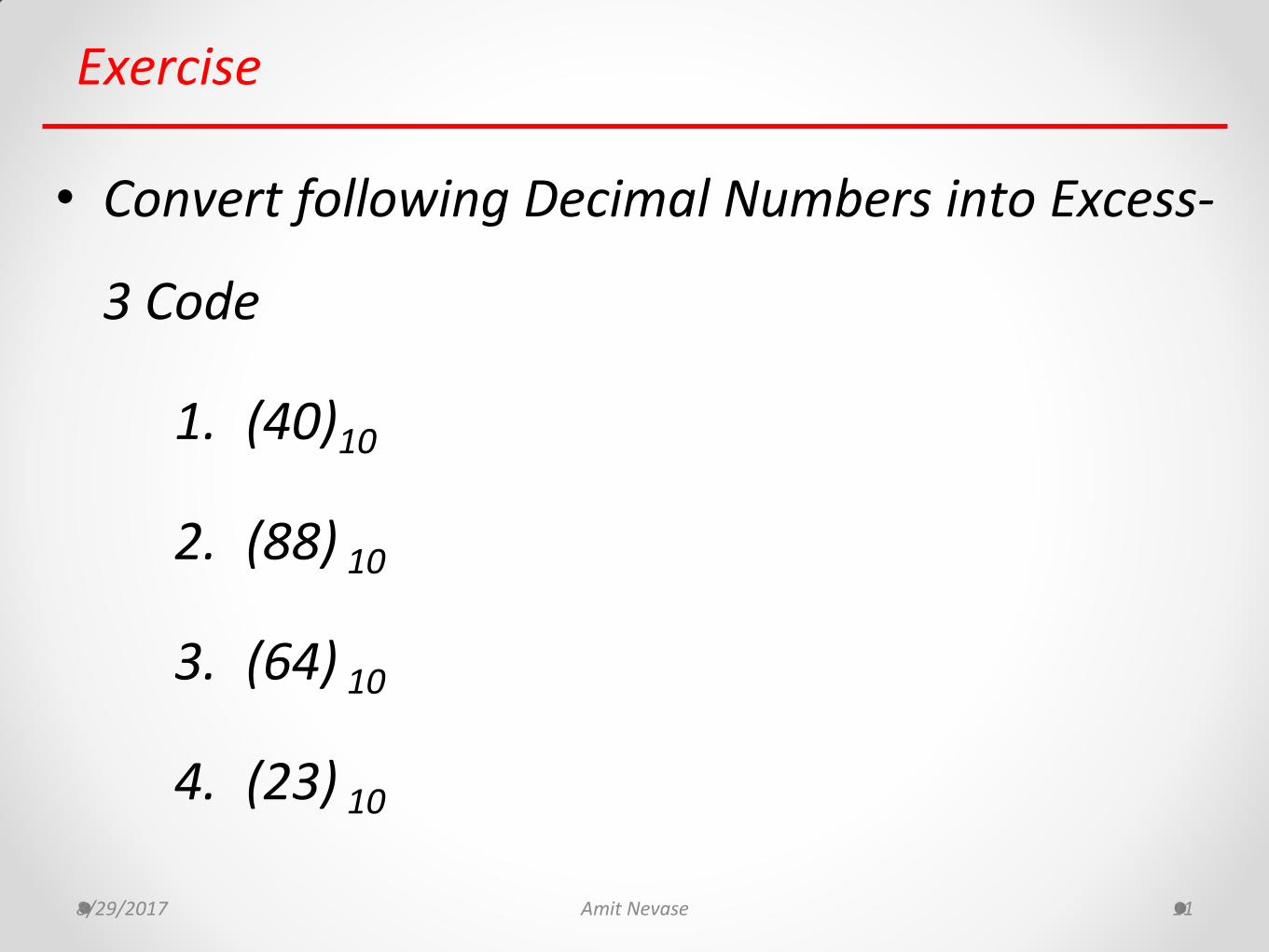
Exercise
• Convert following Decimal Numbers into Excess-
3 Code
1. (40)10
2. (88) 10
3. (64) 10
4. (23) 10

12
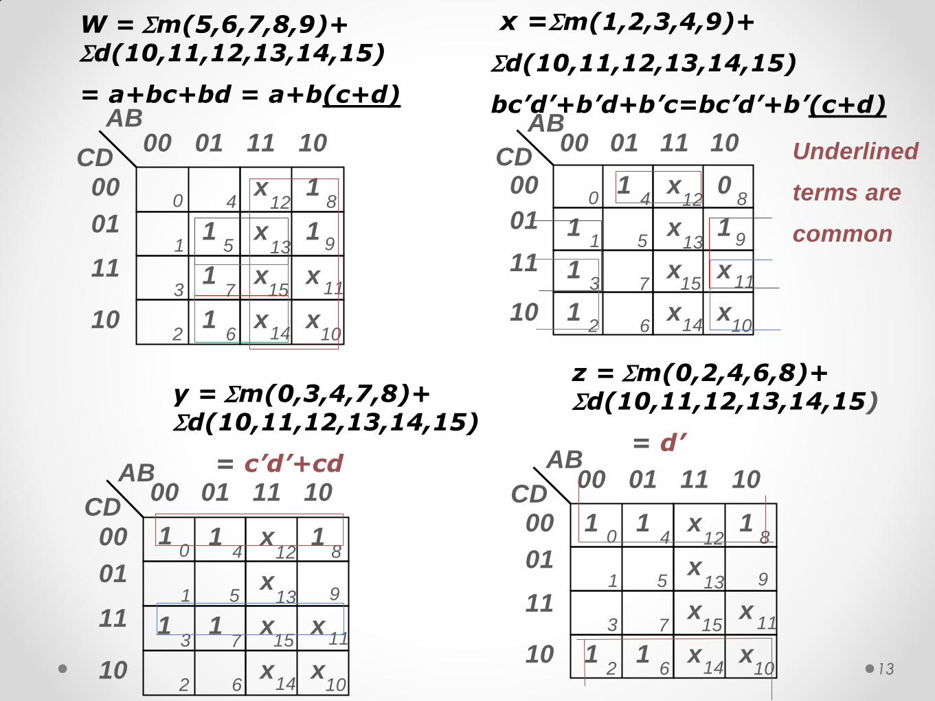
BCD-to-Excess-3 Code Converter
Truth table:
BCD Excess-3
A B C D W X Y Z
0 0 0 0 0 0 0 1 1
1 0 0 0 1 0 1 0 0
2 0 0 1 0 0 1 0 1
3 0 0 1 1 0 1 1 0
4 0 1 0 0 0 1 1 1
5 0 1 0 1 1 0 0 0
6 0 1 1 0 1 0 0 1
7 0 1 1 1 1 0 1 0
8 1 0 0 0 1 0 1 1
9 1 0 0 1 1 1 0 0
10 1 0 1 0 X X X X
11 1 0 1 1 X X X X
12 1 1 0 0 X X X X
13 1 1 0 1 X X X X
14 1 1 1 0 X X X X
15 1 1 1 1 X X X X
W = S m(5,6,7,8,9)
x = S m(1,2,3,4,9)
y = S m(0,3,4,7,8)
z = S m(0,2,4,6,8)
13
AB 01
1
00 CD
00
1
1
01
11
10
x 1
x 1
x x
x x
11 10
0
1
3
2
4
5
7
6
12 8
9
11
10
13
15
14
x =Sm(1,2,3,4,9)+
Sd(10,11,12,13,14,15)
bc’d’+b’d+b’c=bc’d’+b’(c+d)
y = Sm(0,3,4,7,8)+ Sd(10,11,12,13,14,15)
= c’d’+cd
01
1
1
00 CD
00
1
1
01
11
10
x 0
x 1
x x
x x
11 10
0
1
3
2
4
5
7
6
12 8
9
11
10
13
15
14
AB
01
1 1 00 CD
00
1 1
01
11
10
x 1
x
x x
x x
11 10
0
1
3
2
4
5
7
6
12 8
9
11
10
13
15
14
AB
W = Sm(5,6,7,8,9)+
Sd(10,11,12,13,14,15)
= a+bc+bd = a+b(c+d)
z = Sm(0,2,4,6,8)+ Sd(10,11,12,13,14,15)
= d’
01
1 00 CD
00
1 1
01
11
10
x 1
x
x x
x x
11 10
0
1
3
2
4
5
7
6
12 8
9
11
10
13
15
14
AB
1
Underlined
terms are
common

• The Excess-3 BCD system is formed by adding 0011 to each
BCD value as in Table 2. For example, the decimal number 7,
which is coded as 0111 in BCD, is coded as 0111+0011=1010
in Excess-3 BCD.
Decimal Numerals Excess-3
0 0011
1 0100
2 0101
3 0110
4 0111
5 1000
6 1001
7 1010
8 1011
9 1100
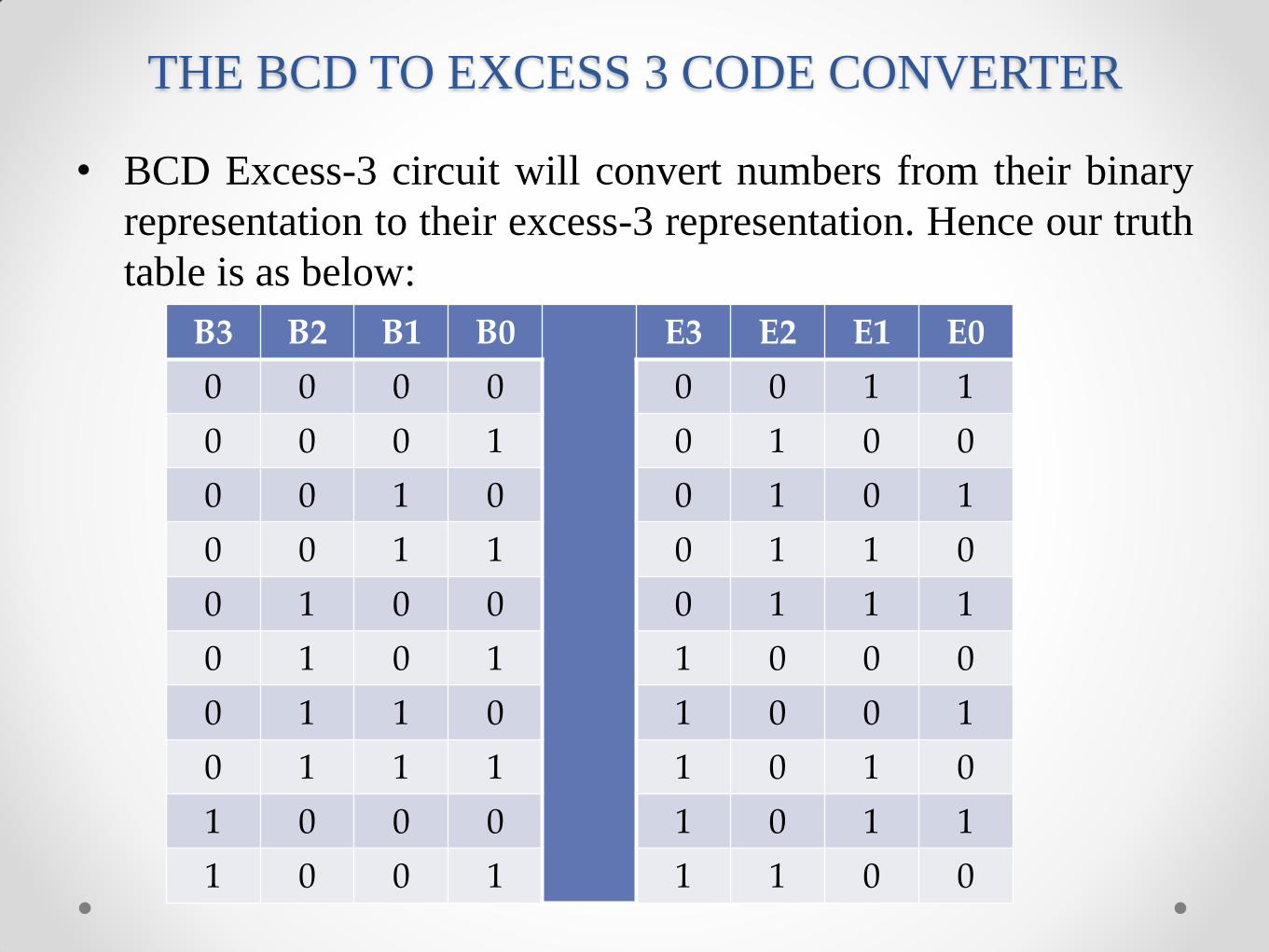
THE BCD TO EXCESS 3 CODE CONVERTER
• BCD Excess-3 circuit will convert numbers from their binary
representation to their excess-3 representation. Hence our truth
table is as below:
B3 B2 B1 B0 E3 E2 E1 E0
0 0 0 0 0 0 1 1
0 0 0 1 0 1 0 0
0 0 1 0 0 1 0 1
0 0 1 1 0 1 1 0
0 1 0 0 0 1 1 1
0 1 0 1 1 0 0 0
0 1 1 0 1 0 0 1
0 1 1 1 1 0 1 0
1 0 0 0 1 0 1 1
1 0 0 1 1 1 0 0
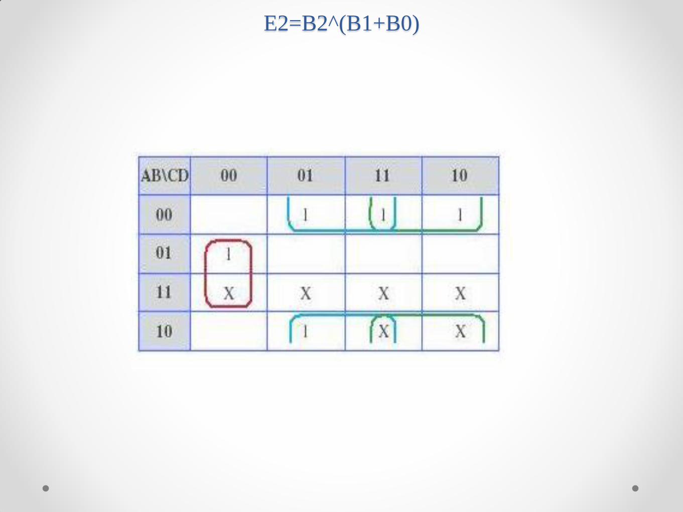
E2=B2^(B1+B0)
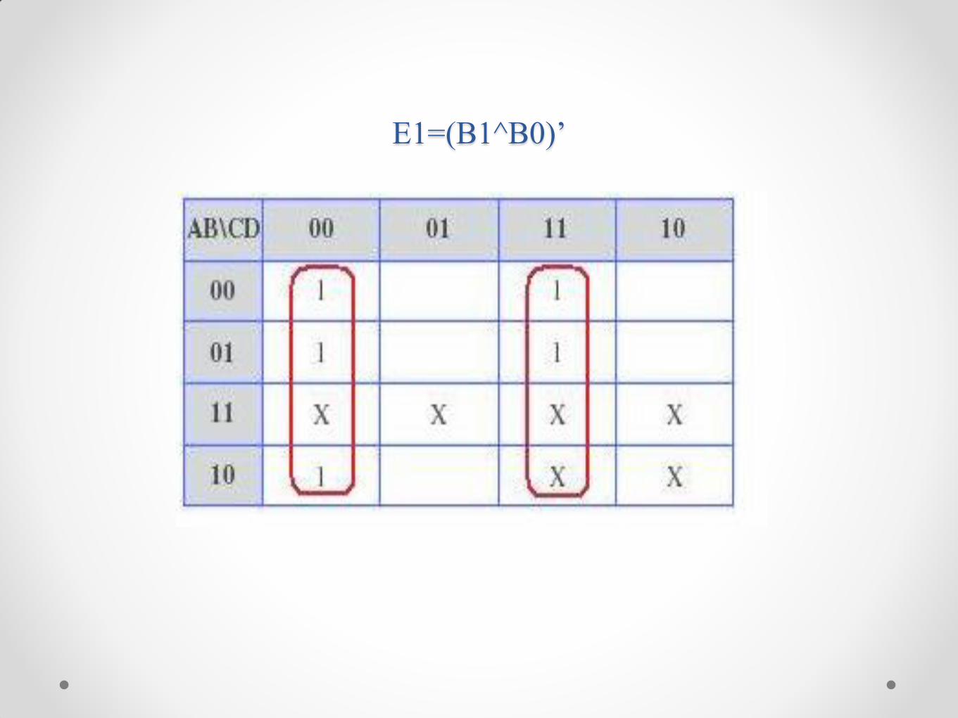
E1=(B1^B0)’
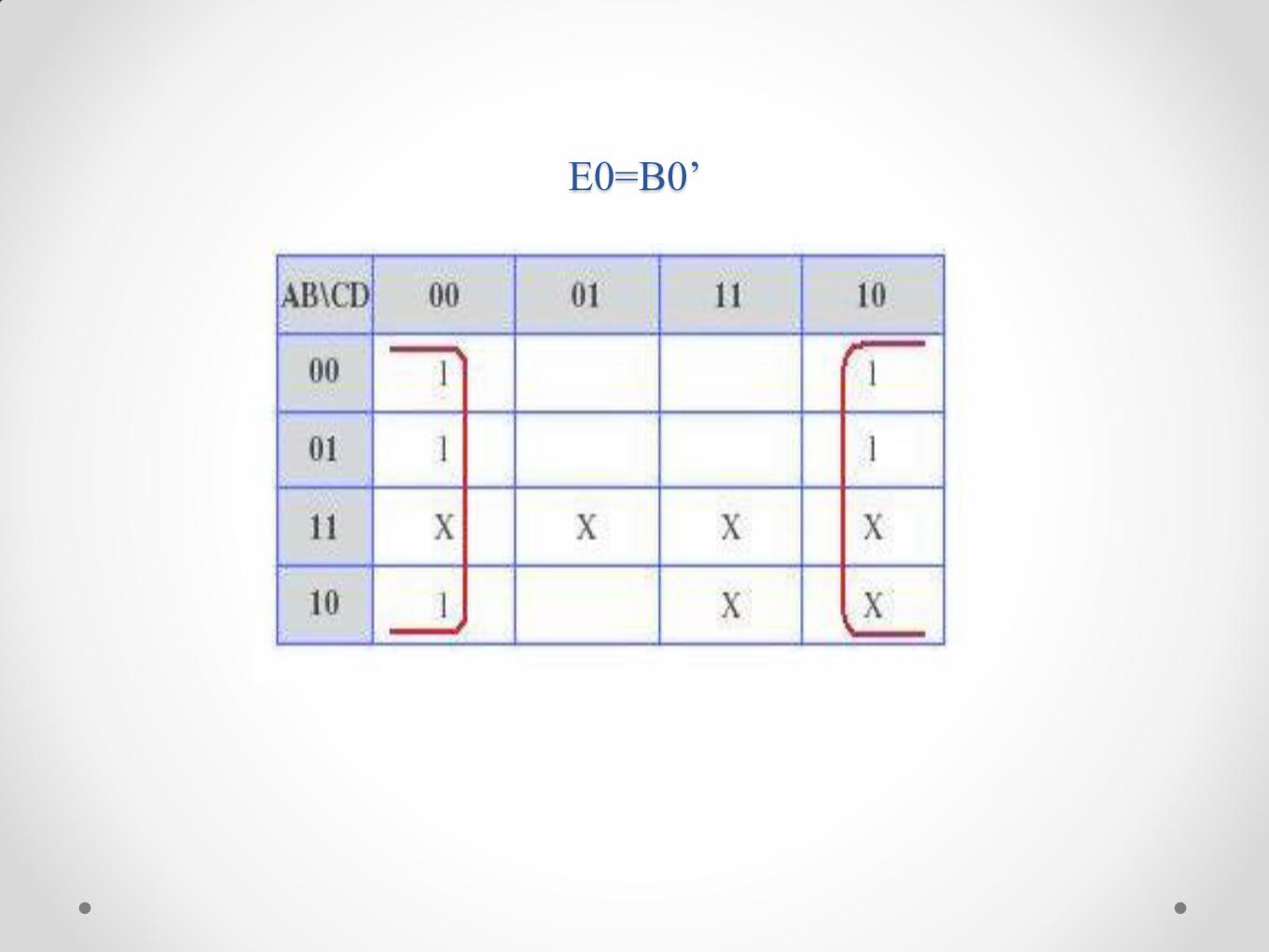
E0=B0’
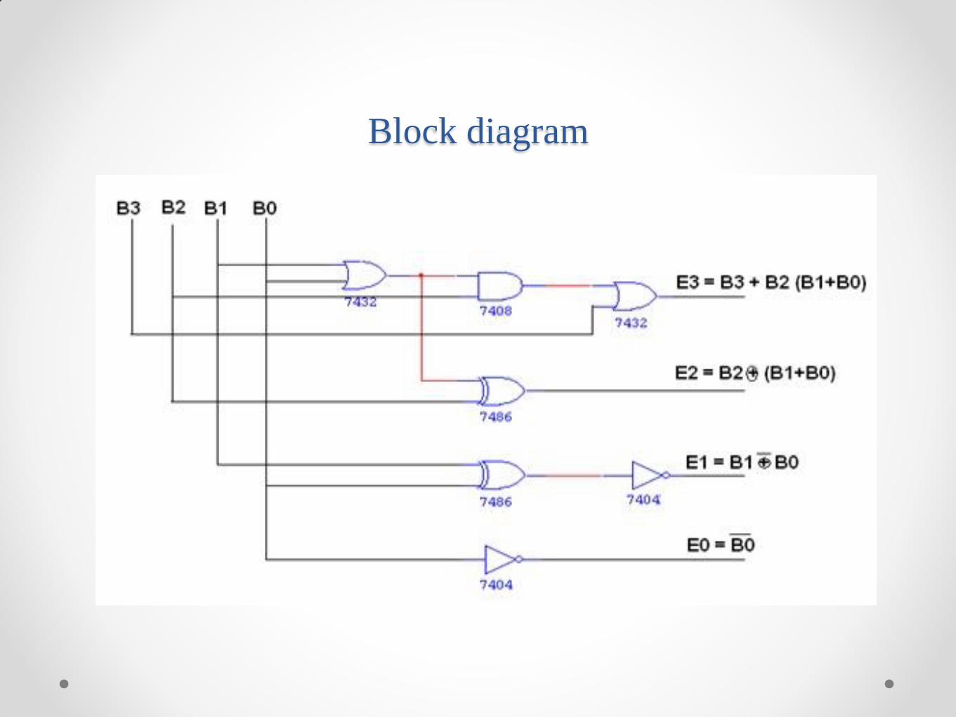
Block diagram
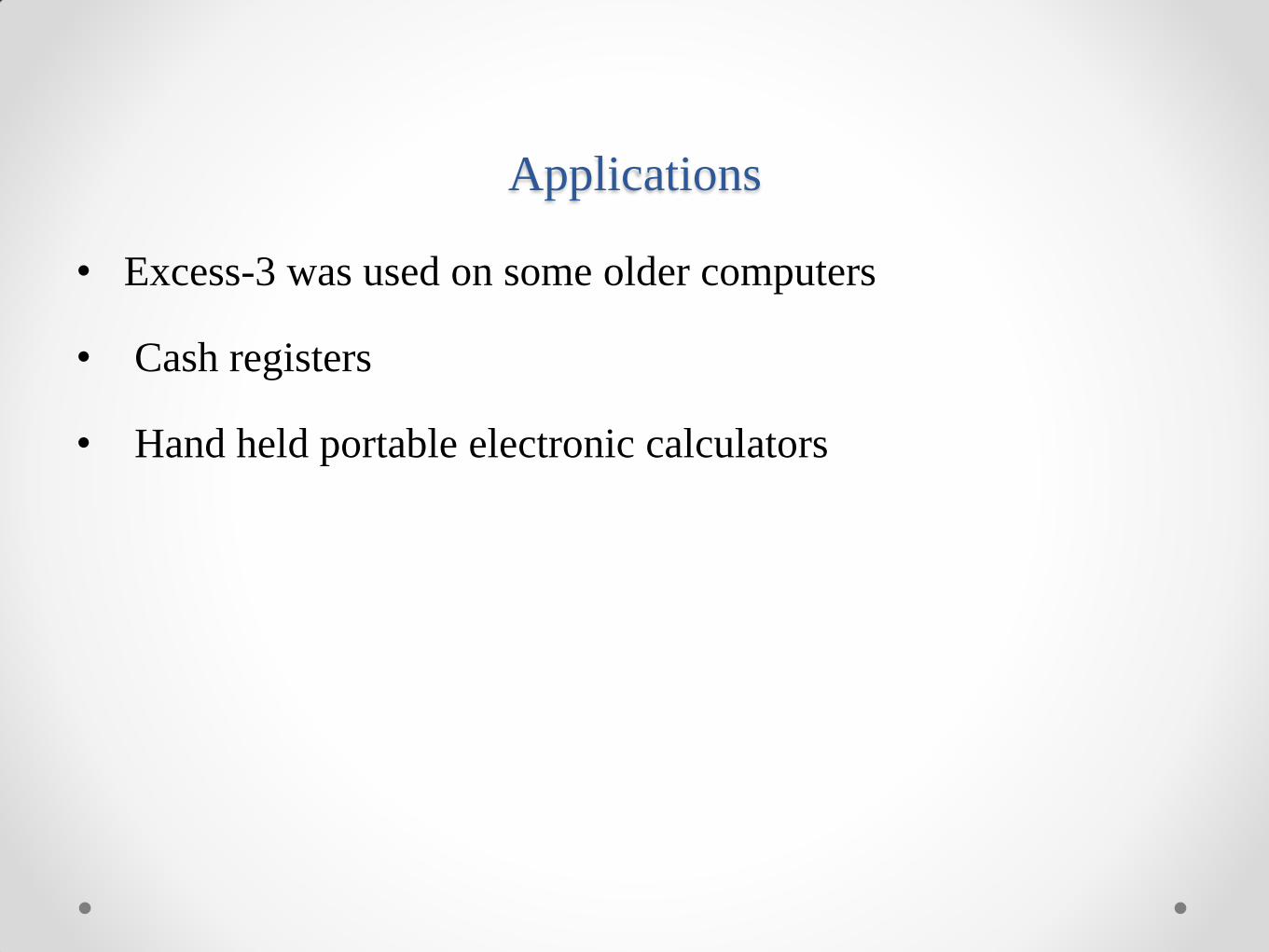
Applications
• Excess-3 was used on some older computers
• Cash registers
• Hand held portable electronic calculators
21
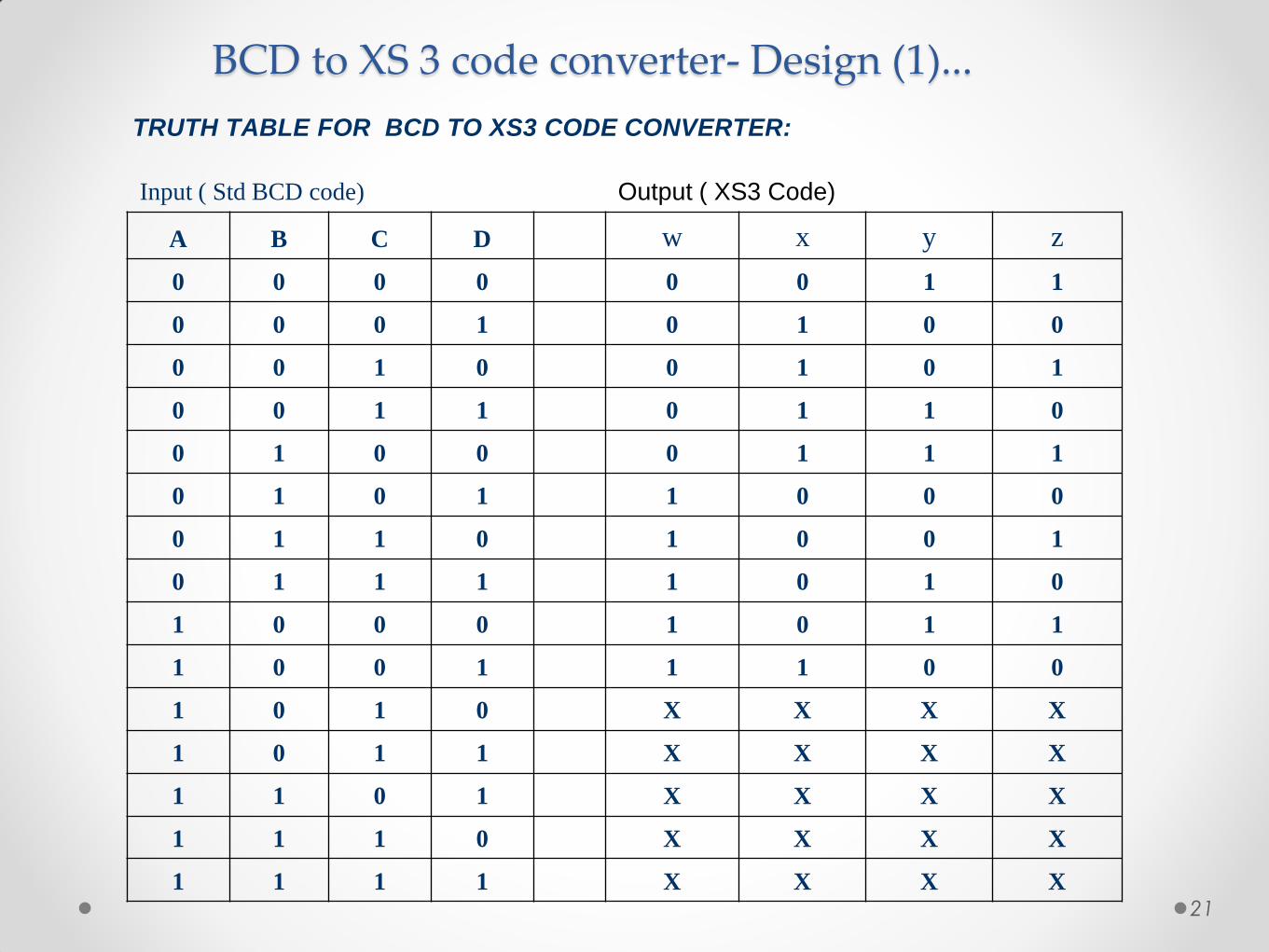
BCD to XS 3 code converter- Design (1)...
TRUTH TABLE FOR BCD TO XS3 CODE CONVERTER:
Input ( Std BCD code) Output ( XS3 Code)
A B C D w x y z
0 0 0 0 0 0 1 1
0 0 0 1 0 1 0 0
0 0 1 0 0 1 0 1
0 0 1 1 0 1 1 0
0 1 0 0 0 1 1 1
0 1 0 1 1 0 0 0
0 1 1 0 1 0 0 1
0 1 1 1 1 0 1 0
1 0 0 0 1 0 1 1
1 0 0 1 1 1 0 0
1 0 1 0 X X X X
1 0 1 1 X X X X
1 1 0 1 X X X X
1 1 1 0 X X X X
1 1 1 1 X X X X
22
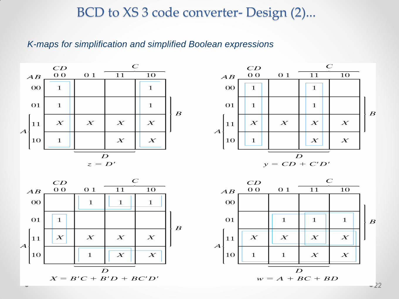
BCD to XS 3 code converter- Design (2)...
K-maps for simplification and simplified Boolean expressions

23
BCD to XS 3 code converter- Design (3)...
• After the manipulation of the Boolean expressions
for using common gates for two or more outputs,
logic expressions can be given by
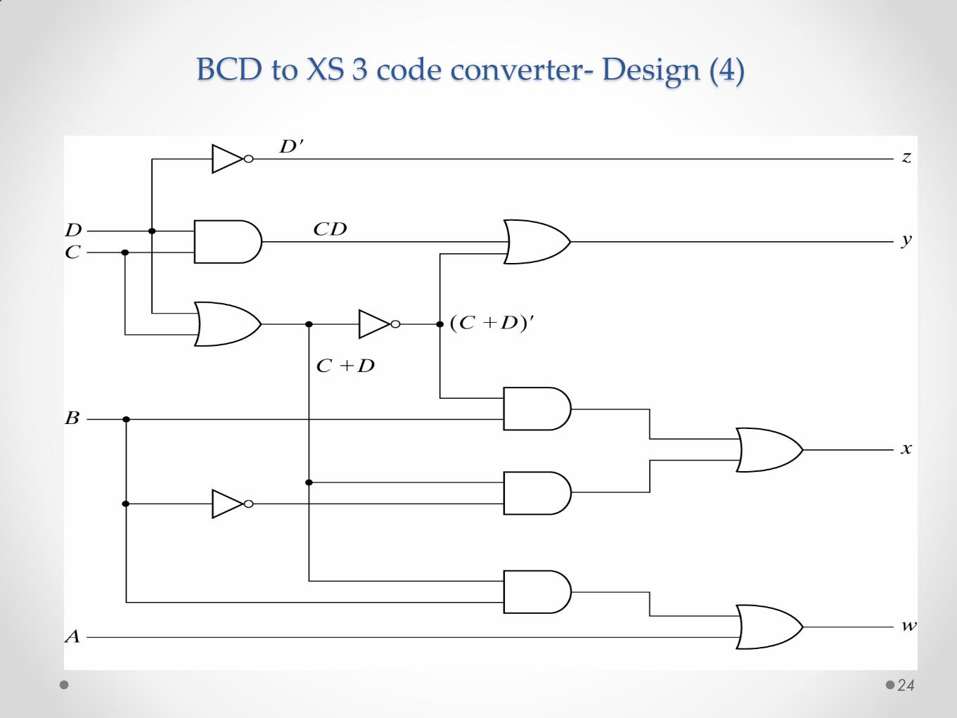
z=D’
y=CD+C’D’ = (C+D)’
x= B’C + B’D + BC’D’ = B’(C+D) + BC’D’
w= A + BC + BD = A + B (C+D)
24
BCD to XS 3 code converter- Design (4)
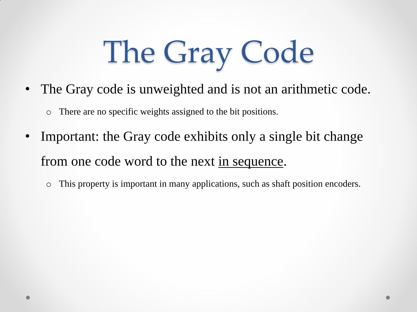
The Gray Code • The Gray code is unweighted and is not an arithmetic code.
o There are no specific weights assigned to the bit positions.
• Important: the Gray code exhibits only a single bit change
from one code word to the next in sequence.
o This property is important in many applications, such as shaft position encoders.
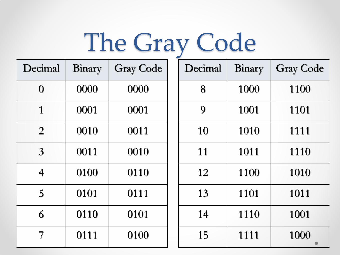
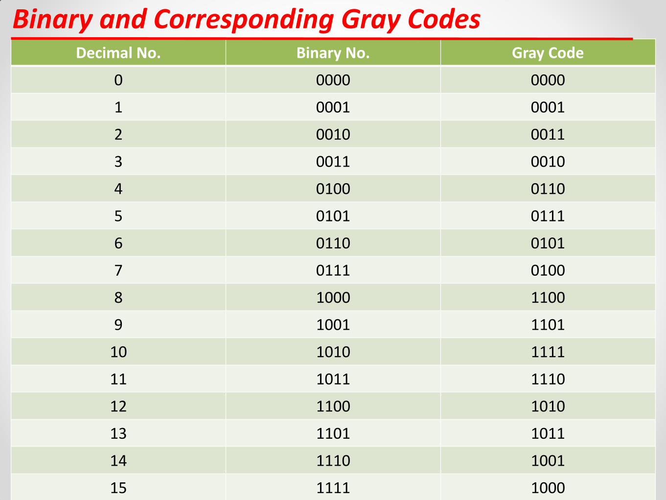
The Gray Code Decimal Binary Gray Code
0 0000 0000
1 0001 0001
2 0010 0011
3 0011 0010
4 0100 0110
5 0101 0111
6 0110 0101
7 0111 0100
Decimal Binary Gray Code
8 1000 1100
9 1001 1101
10 1010 1111
11 1011 1110
12 1100 1010
13 1101 1011
14 1110 1001
15 1111 1000
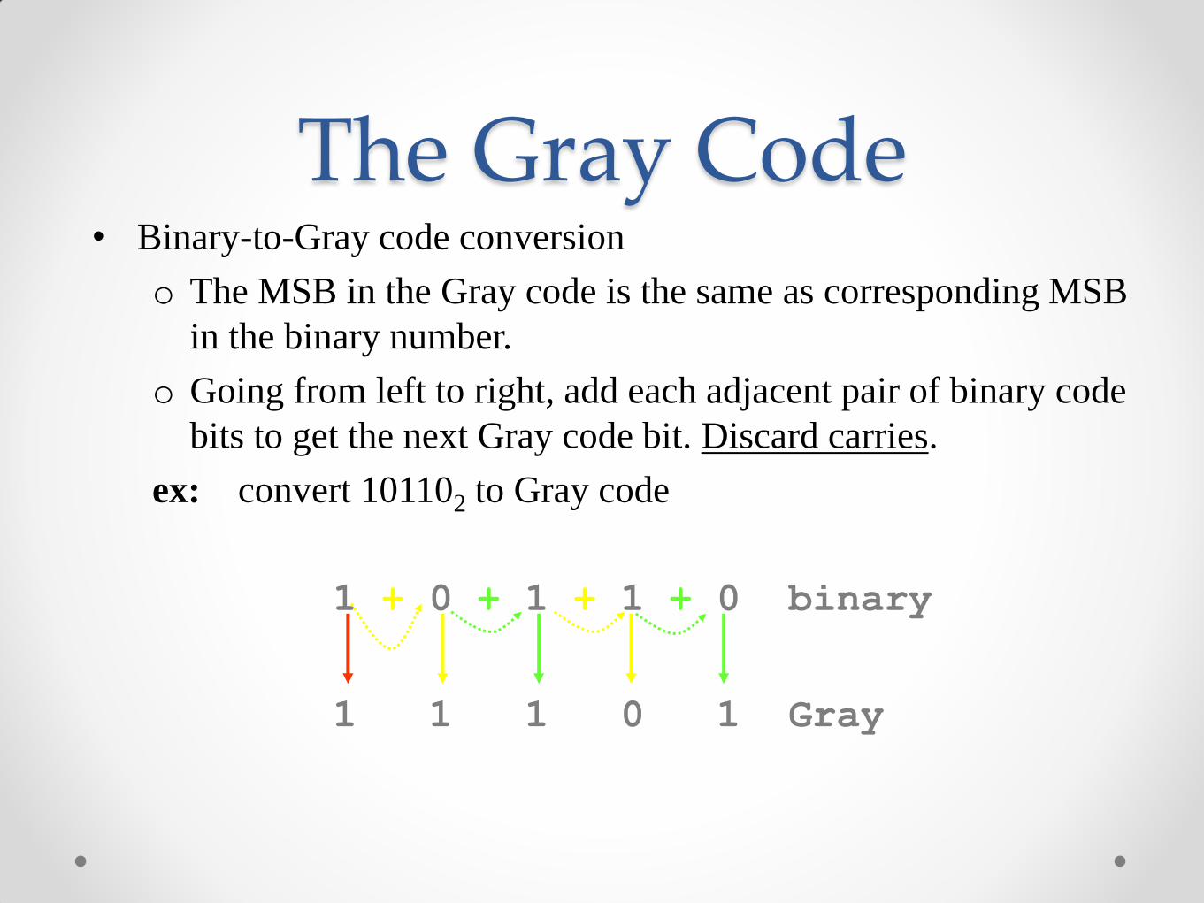
The Gray Code • Binary-to-Gray code conversion
o The MSB in the Gray code is the same as corresponding MSB
in the binary number.
o Going from left to right, add each adjacent pair of binary code
bits to get the next Gray code bit. Discard carries.
ex: convert 101102 to Gray code
1 + 0 + 1 + 1 + 0 binary
1 1 1 0 1 Gray
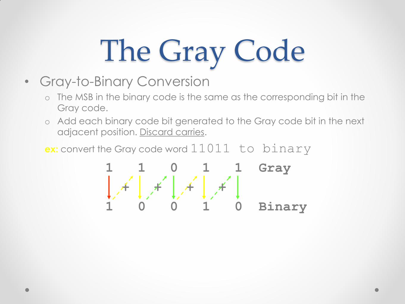
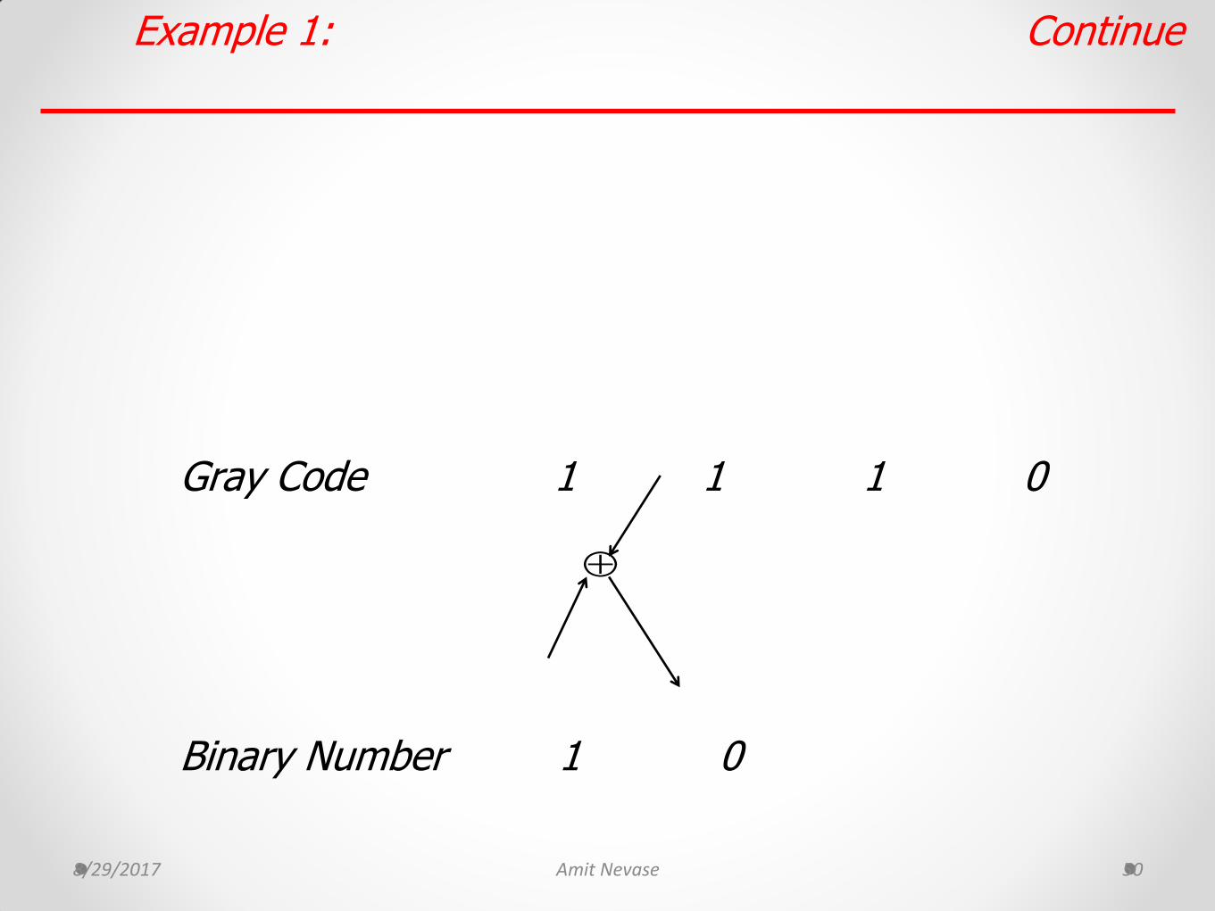
The Gray Code • Gray-to-Binary Conversion
o The MSB in the binary code is the same as the corresponding bit in the Gray code.
o Add each binary code bit generated to the Gray code bit in the next
adjacent position. Discard carries.
ex: convert the Gray code word 11011 to binary
1 1 0 1 1 Gray
+ + + +
1 0 0 1 0 Binary
Gray Code
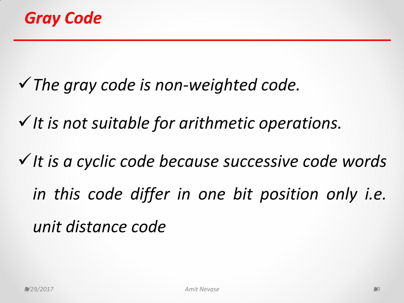
The gray code is non-weighted code.
It is not suitable for arithmetic operations.
It is a cyclic code because successive code words
in this code differ in one bit position only i.e.
unit distance code
8/29/2017 Amit Nevase 29
Binary to Gray Code Conversion
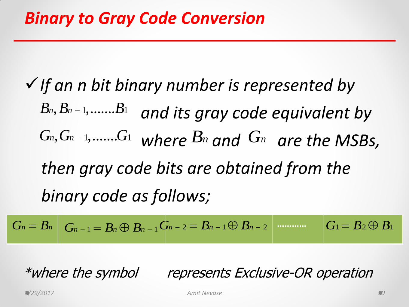
If an n bit binary number is represented by
and its gray code equivalent by
where and are the MSBs,
then gray code bits are obtained from the
binary code as follows;
8/29/2017 Amit Nevase 30
…………
*where the symbol represents Exclusive-OR operation
1 1, ,.......n nB B B
1 1, ,.......n nG G G nB nG
n nG B 1 1n n nG B B 2 1 2n n nG B B 1 2 1G B B

8/29/2017 Amit Nevase 31
Binary to Gray Code Conversion
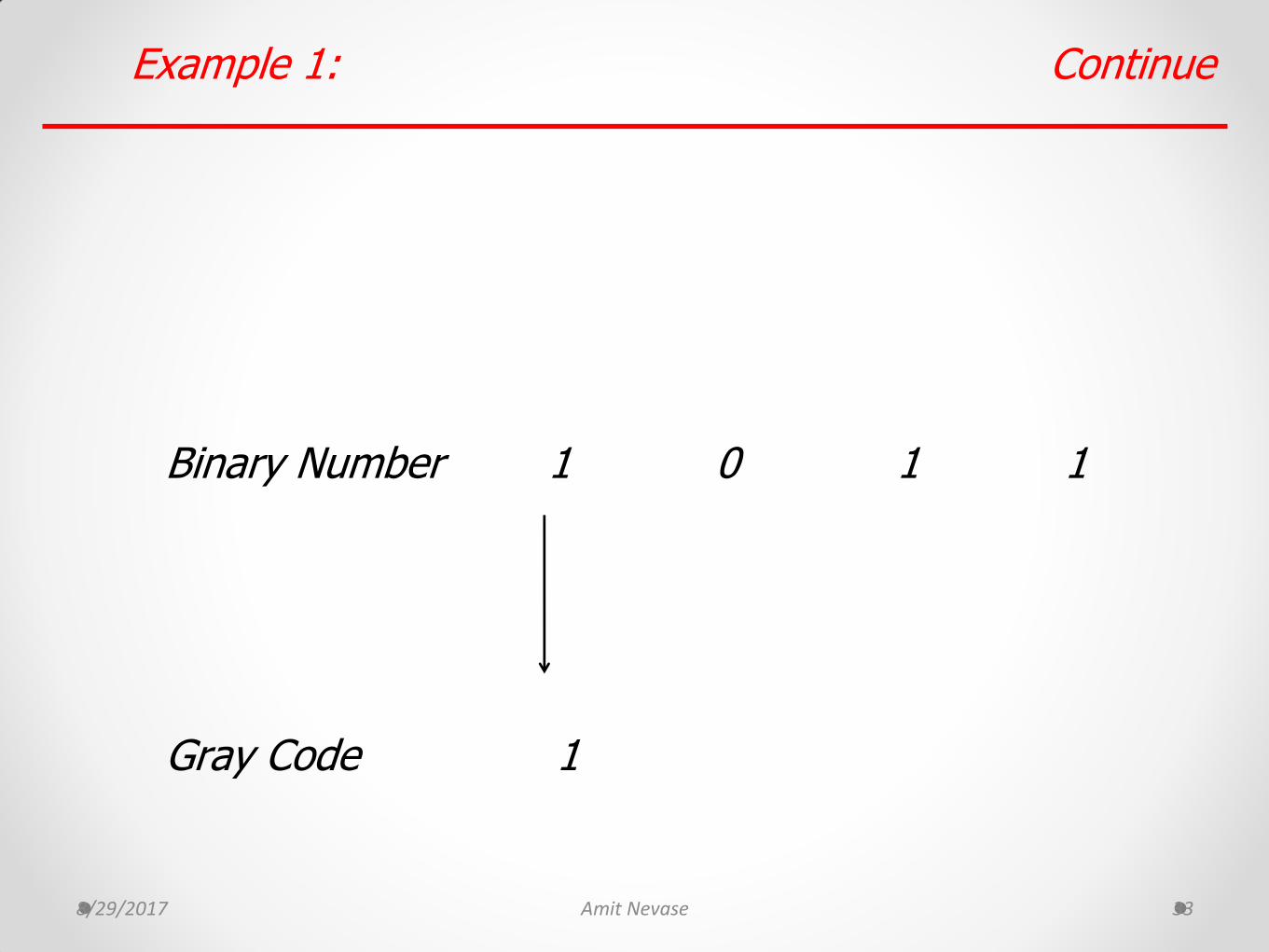
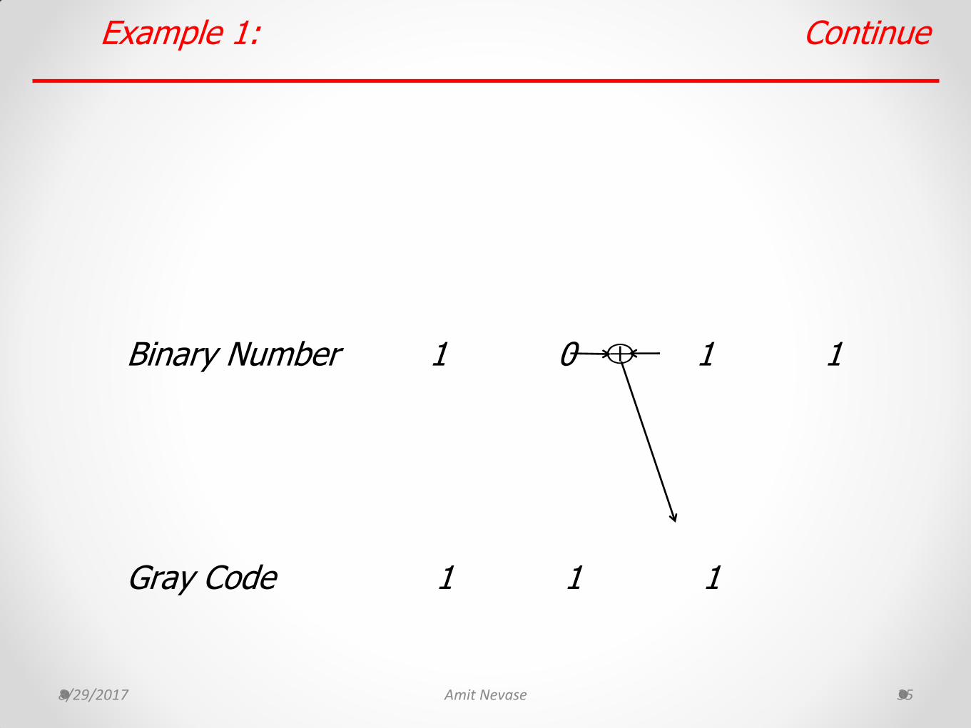
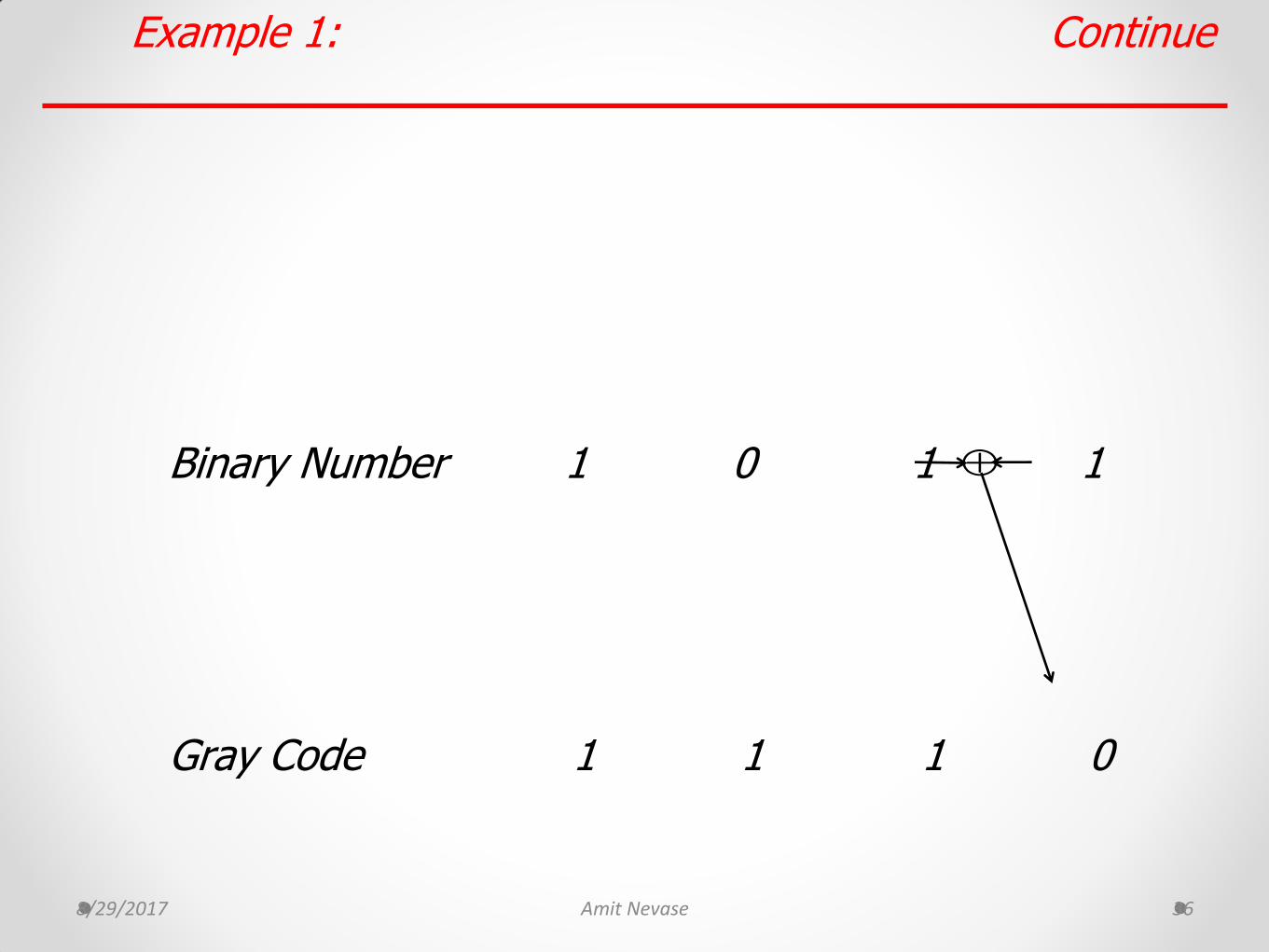
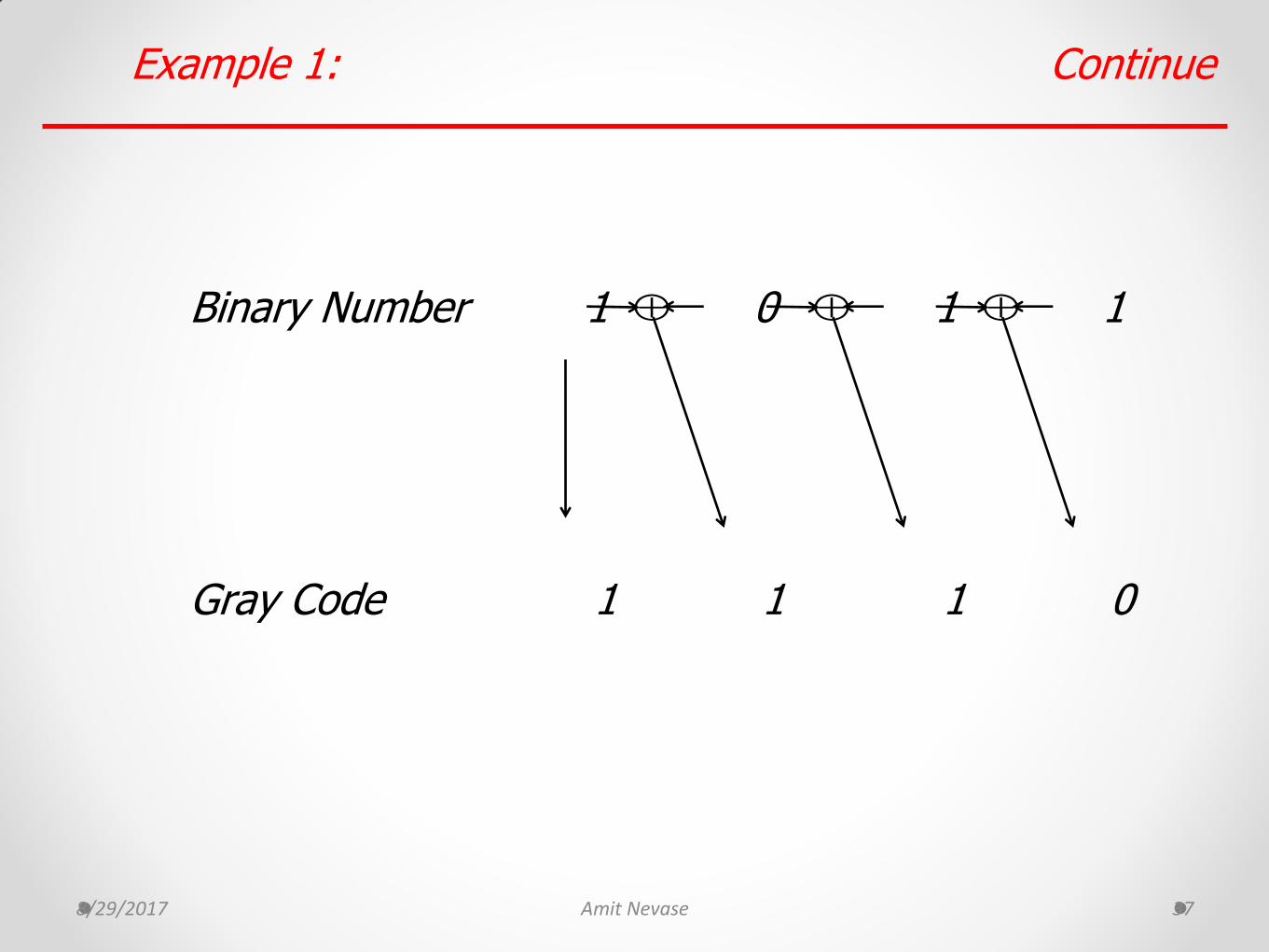
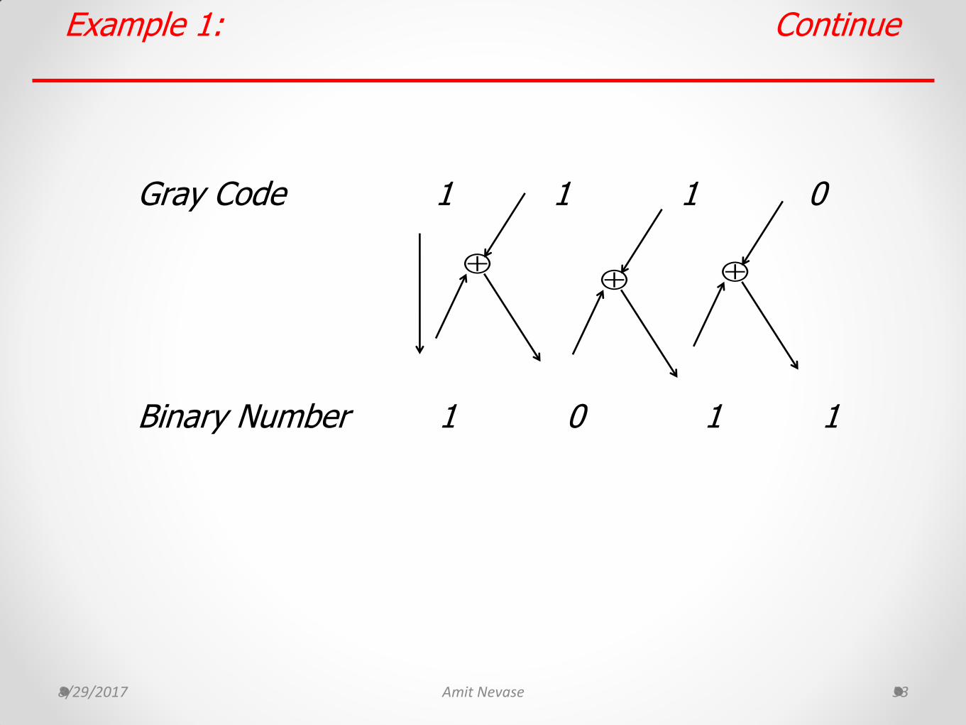
Example 1: Convert 1011 Binary Number into Gray Code
8/29/2017 Amit Nevase 32
Binary to Gray Code Conversion
Example 1: Convert 1011 Binary Number into Gray Code
Binary Number 1 0 1 1
8/29/2017 Amit Nevase 33
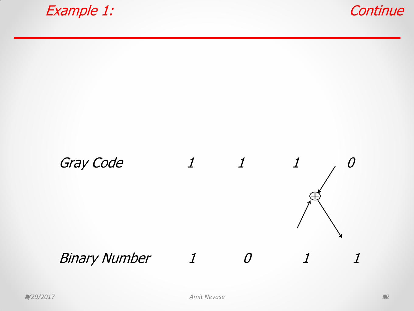
Binary Number 1 0 1 1
Gray Code 1
Example 1: Continue

8/29/2017 Amit Nevase 34
Example 1: Continue
Binary Number 1 0 1 1
Gray Code 1 1
8/29/2017 Amit Nevase 35
Binary Number 1 0 1 1
Gray Code 1 1 1
Example 1: Continue
8/29/2017 Amit Nevase 36
Binary Number 1 0 1 1
Gray Code 1 1 1 0
Example 1: Continue
8/29/2017 Amit Nevase 37
Binary Number 1 0 1 1
Gray Code 1 1 1 0
Example 1: Continue
Binary to Gray Code Conversion
8/29/2017 Amit Nevase 38
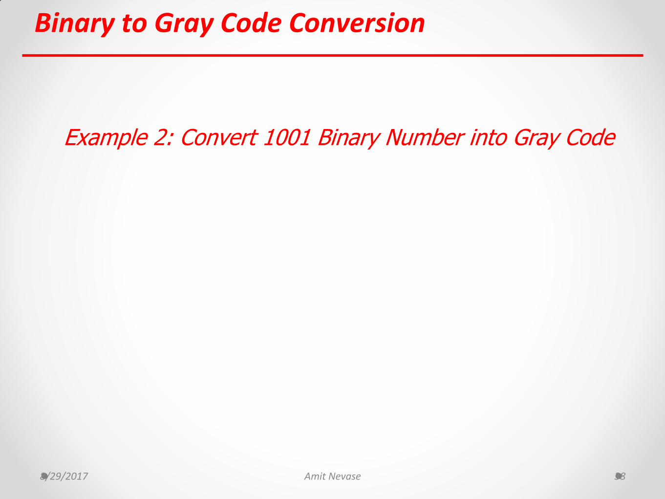
Example 2: Convert 1001 Binary Number into Gray Code

Binary to Gray Code Conversion
8/29/2017 Amit Nevase 39
Example 2: Convert 1001 Binary Number into Gray Code
Binary Number 1 0 0 1
Gray Code 1 1 0 1
Binary to Gray Code Conversion
8/29/2017 Amit Nevase 40
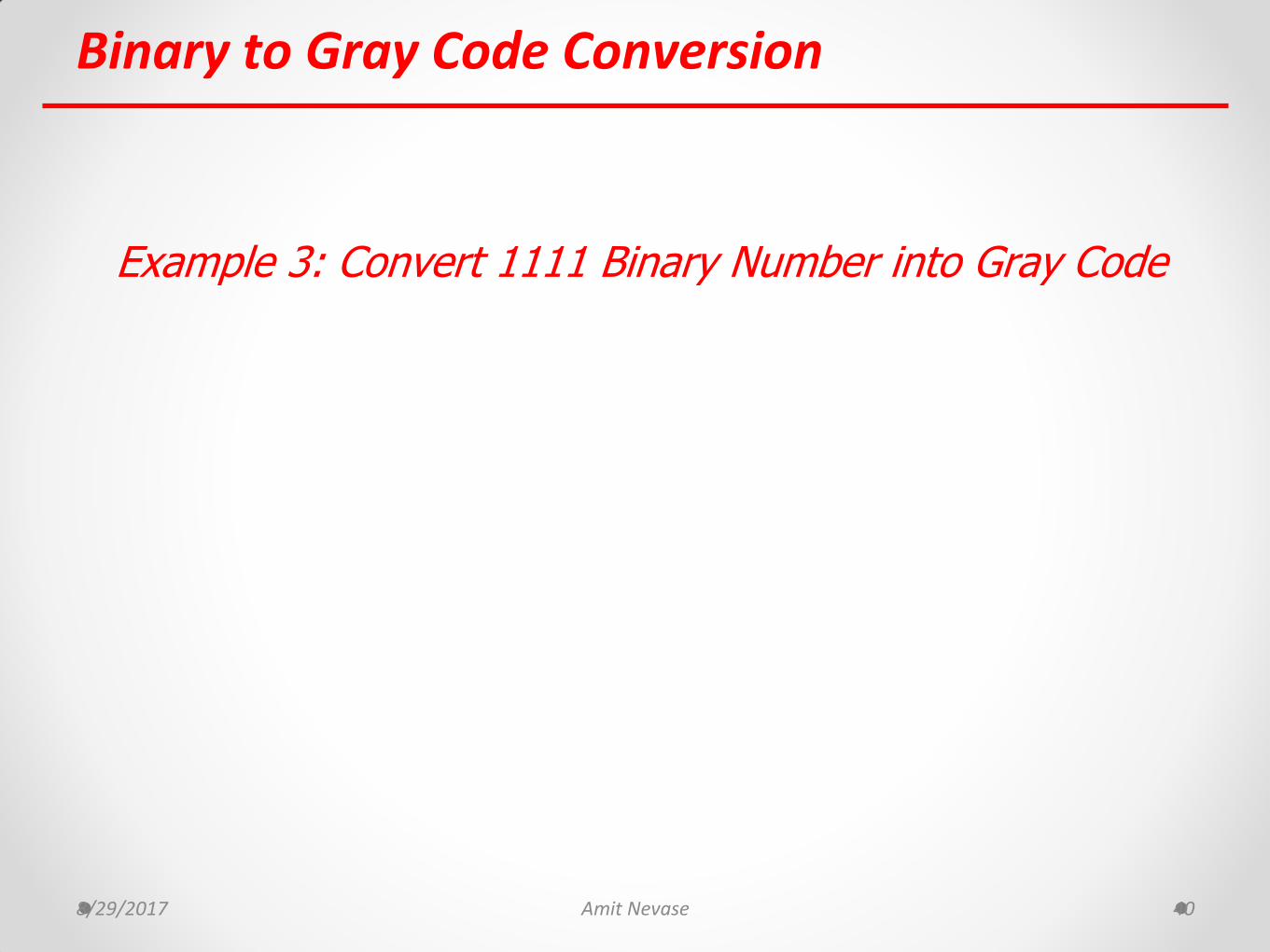
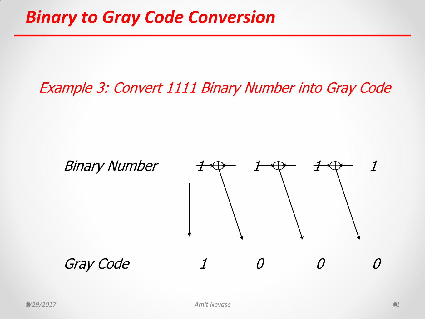
Example 3: Convert 1111 Binary Number into Gray Code
Binary to Gray Code Conversion
8/29/2017 Amit Nevase 41
Example 3: Convert 1111 Binary Number into Gray Code
Binary Number 1 1 1 1
Gray Code 1 0 0 0
Binary to Gray Code Conversion
8/29/2017 Amit Nevase 42
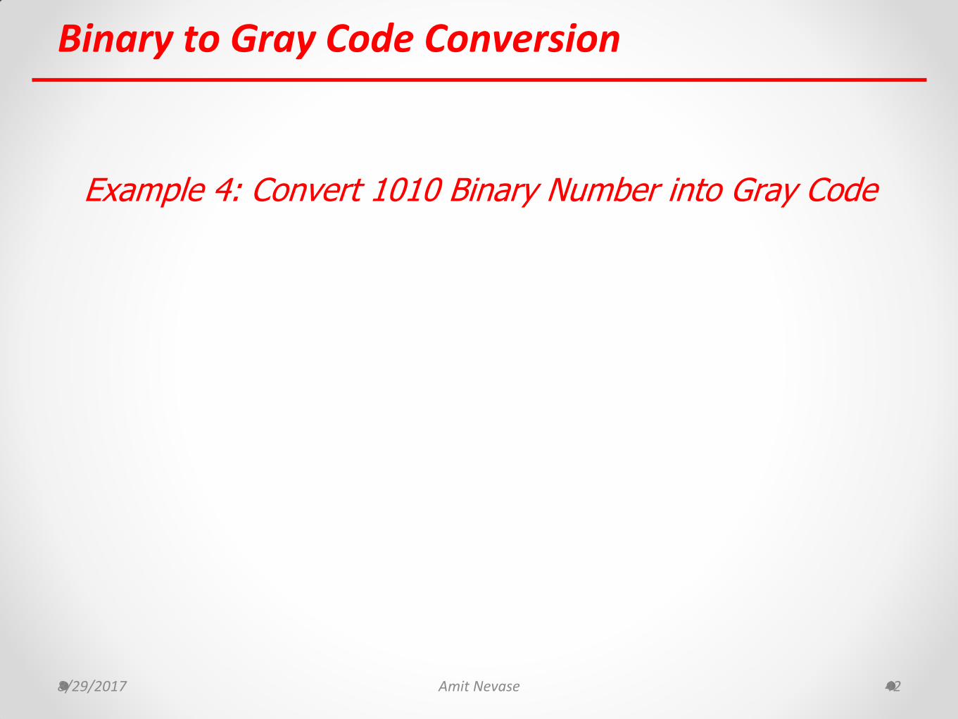
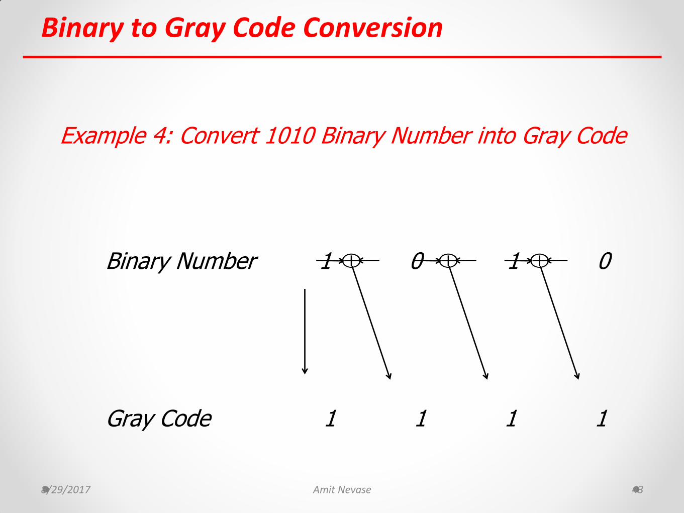
Example 4: Convert 1010 Binary Number into Gray Code
Binary to Gray Code Conversion
8/29/2017 Amit Nevase 43
Example 4: Convert 1010 Binary Number into Gray Code
Binary Number 1 0 1 0
Gray Code 1 1 1 1
Binary and Corresponding Gray Codes
8/29/2017 Amit Nevase 44
Decimal No. Binary No. Gray Code
0 0000 0000
1 0001 0001
2 0010 0011
3 0011 0010
4 0100 0110
5 0101 0111
6 0110 0101
7 0111 0100
8 1000 1100
9 1001 1101
10 1010 1111
11 1011 1110
12 1100 1010
13 1101 1011
14 1110 1001
15 1111 1000
8/29/2017 Amit Nevase 45
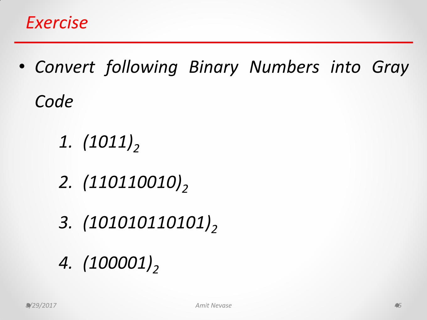
Exercise
• Convert following Binary Numbers into Gray
Code
1. (1011)2
2. (110110010)2
3. (101010110101)2
4. (100001)2
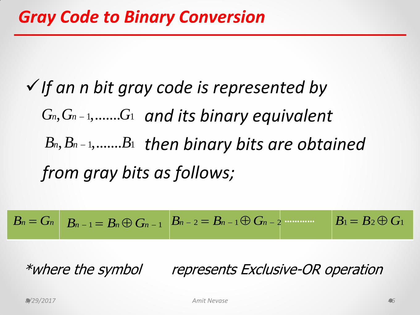
Gray Code to Binary Conversion
If an n bit gray code is represented by
and its binary equivalent
then binary bits are obtained
from gray bits as follows;
8/29/2017 Amit Nevase 46
…………
*where the symbol represents Exclusive-OR operation
1 1, ,.......n nG G G
1 1, ,.......n nB B B
n nB G 1 1n n nB B G 2 1 2n n nB B G 1 2 1B B G
Gray Code to Binary Conversion
8/29/2017 Amit Nevase 47
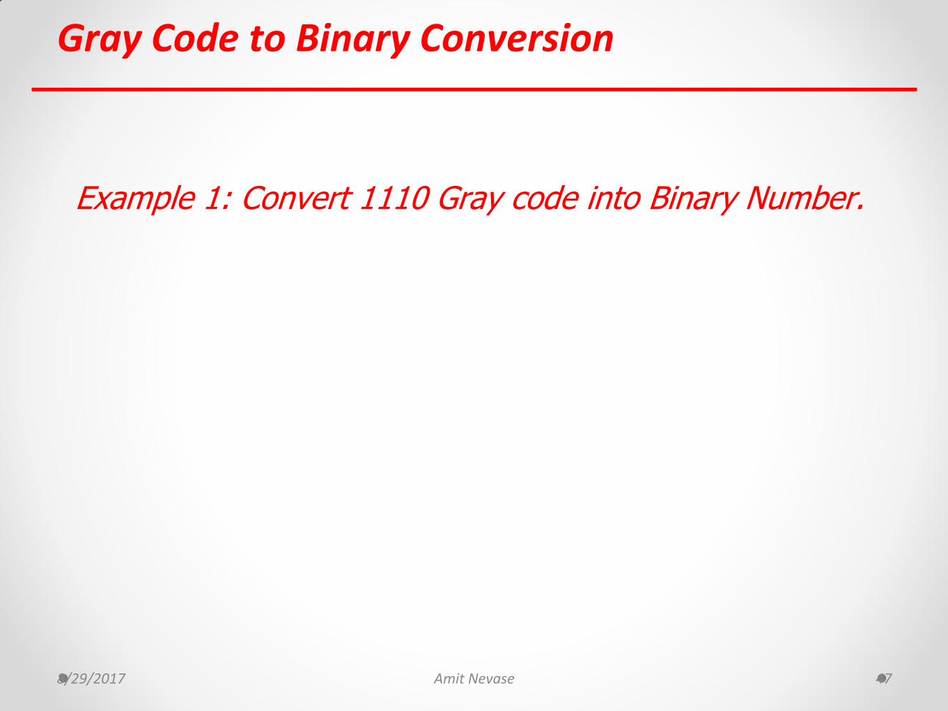
Example 1: Convert 1110 Gray code into Binary Number.
Gray Code to Binary Conversion
8/29/2017 Amit Nevase 48
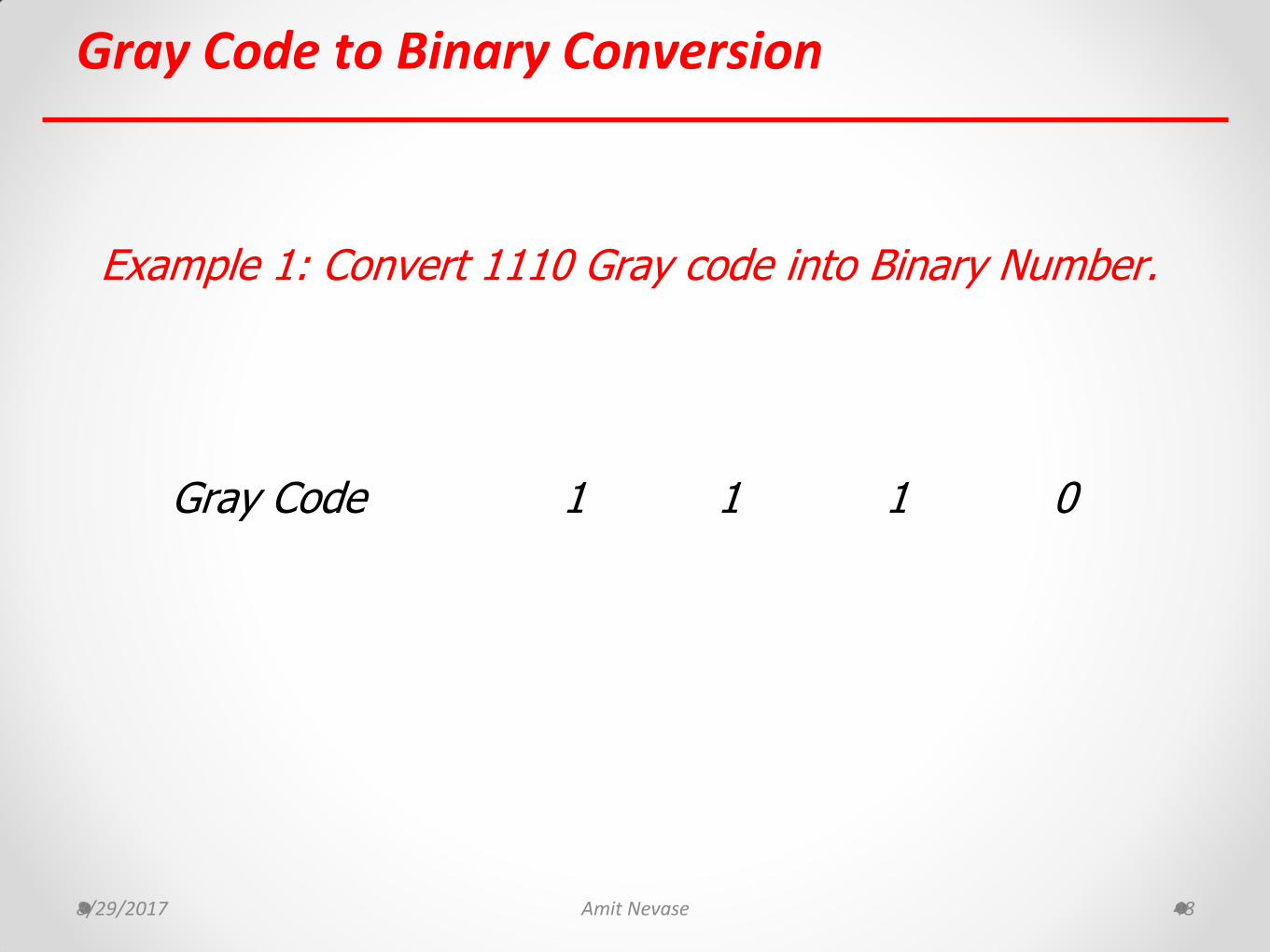
Example 1: Convert 1110 Gray code into Binary Number.
Gray Code 1 1 1 0
8/29/2017 Amit Nevase 49
Example 1: Continue
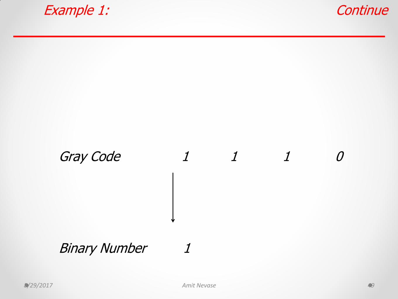
Gray Code 1 1 1 0
Binary Number 1
8/29/2017 Amit Nevase 50
Gray Code 1 1 1 0
Binary Number 1 0
Example 1: Continue

8/29/2017 Amit Nevase 51
Gray Code 1 1 1 0
Binary Number 1 0 1
Example 1: Continue
8/29/2017 Amit Nevase 52
Gray Code 1 1 1 0
Binary Number 1 0 1 1
Example 1: Continue
8/29/2017 Amit Nevase 53
Gray Code 1 1 1 0
Binary Number 1 0 1 1
Example 1: Continue
Gray Code to Binary Conversion
8/29/2017 Amit Nevase 54
Example 2: Convert 1101 Gray code into Binary Number.
Gray Code to Binary Conversion
8/29/2017 Amit Nevase 55
Example 2: Convert 1101 Gray code into Binary Number.
Gray Code 1 1 0 1
Binary Number 1 0 0 1
8/29/2017 Amit Nevase 56
Gray Code to Binary Conversion
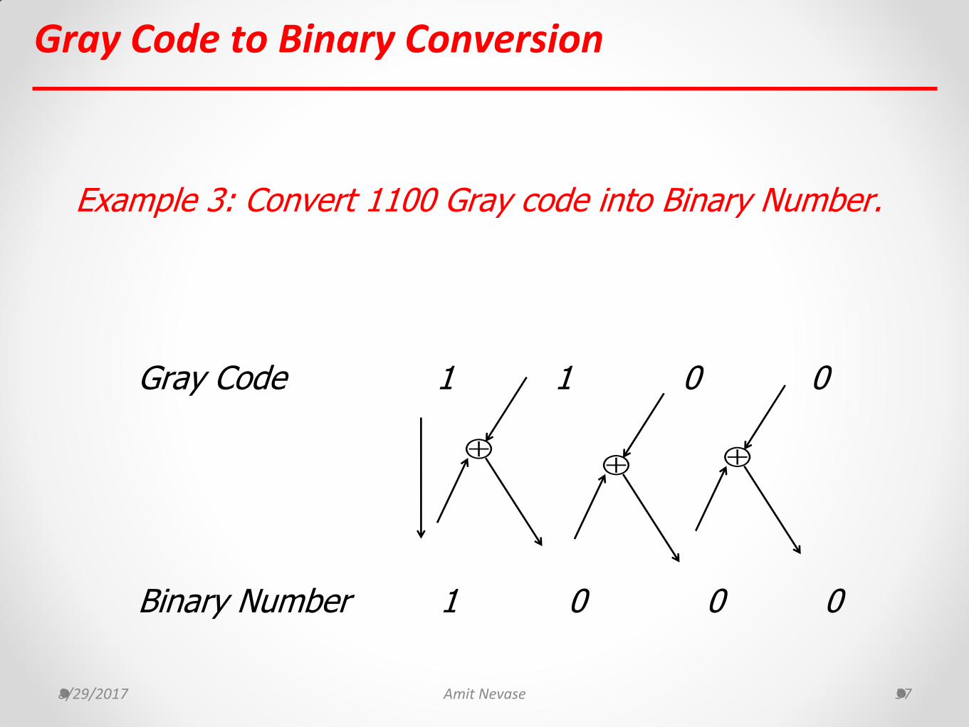
Example 3: Convert 1100 Gray code into Binary Number.
8/29/2017 Amit Nevase 57
Gray Code to Binary Conversion
Example 3: Convert 1100 Gray code into Binary Number.
Gray Code 1 1 0 0
Binary Number 1 0 0 0
8/29/2017 Amit Nevase 58
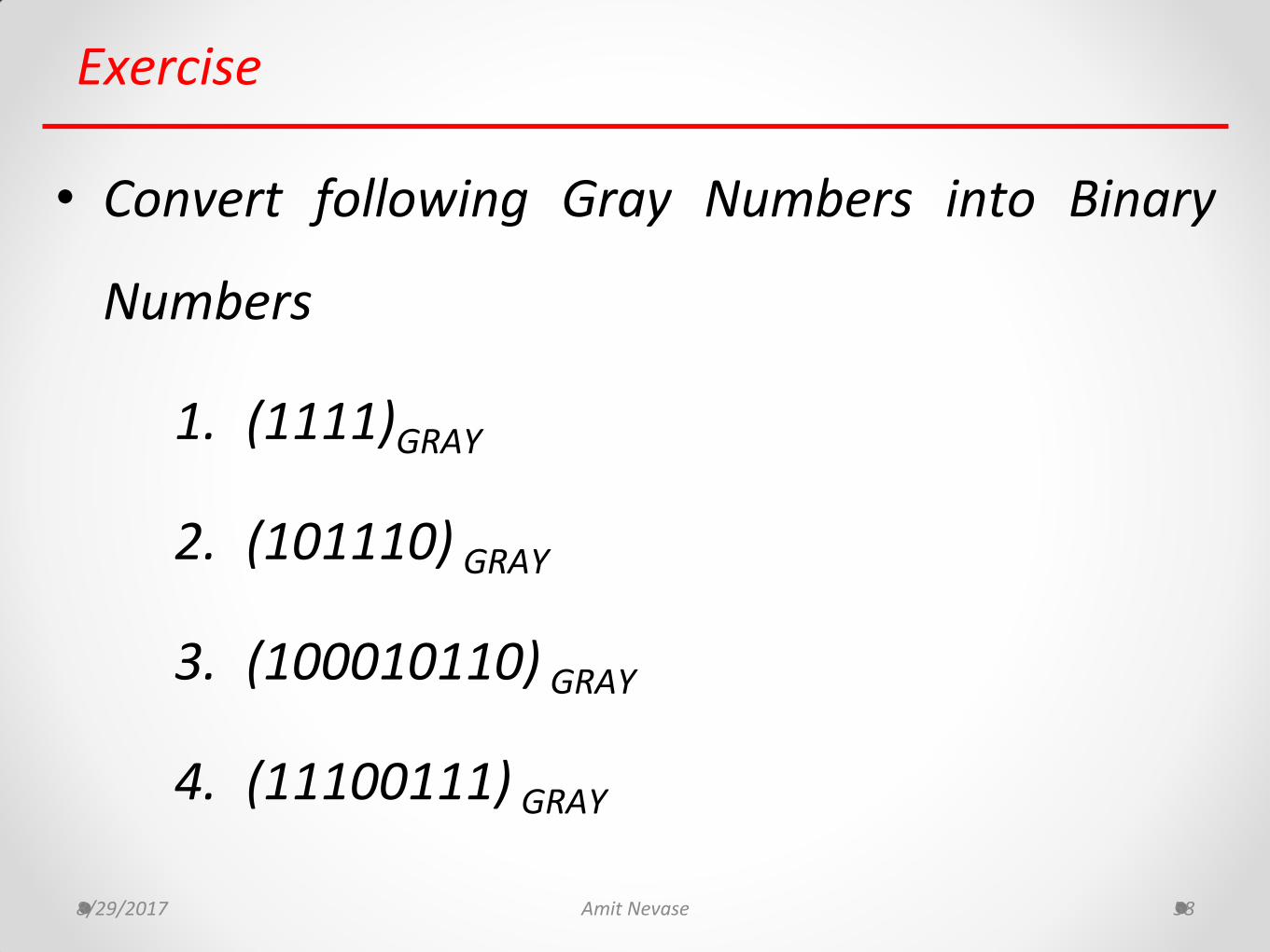
Exercise
• Convert following Gray Numbers into Binary
Numbers
1. (1111)GRAY
2. (101110) GRAY
3. (100010110) GRAY
4. (11100111) GRAY
59
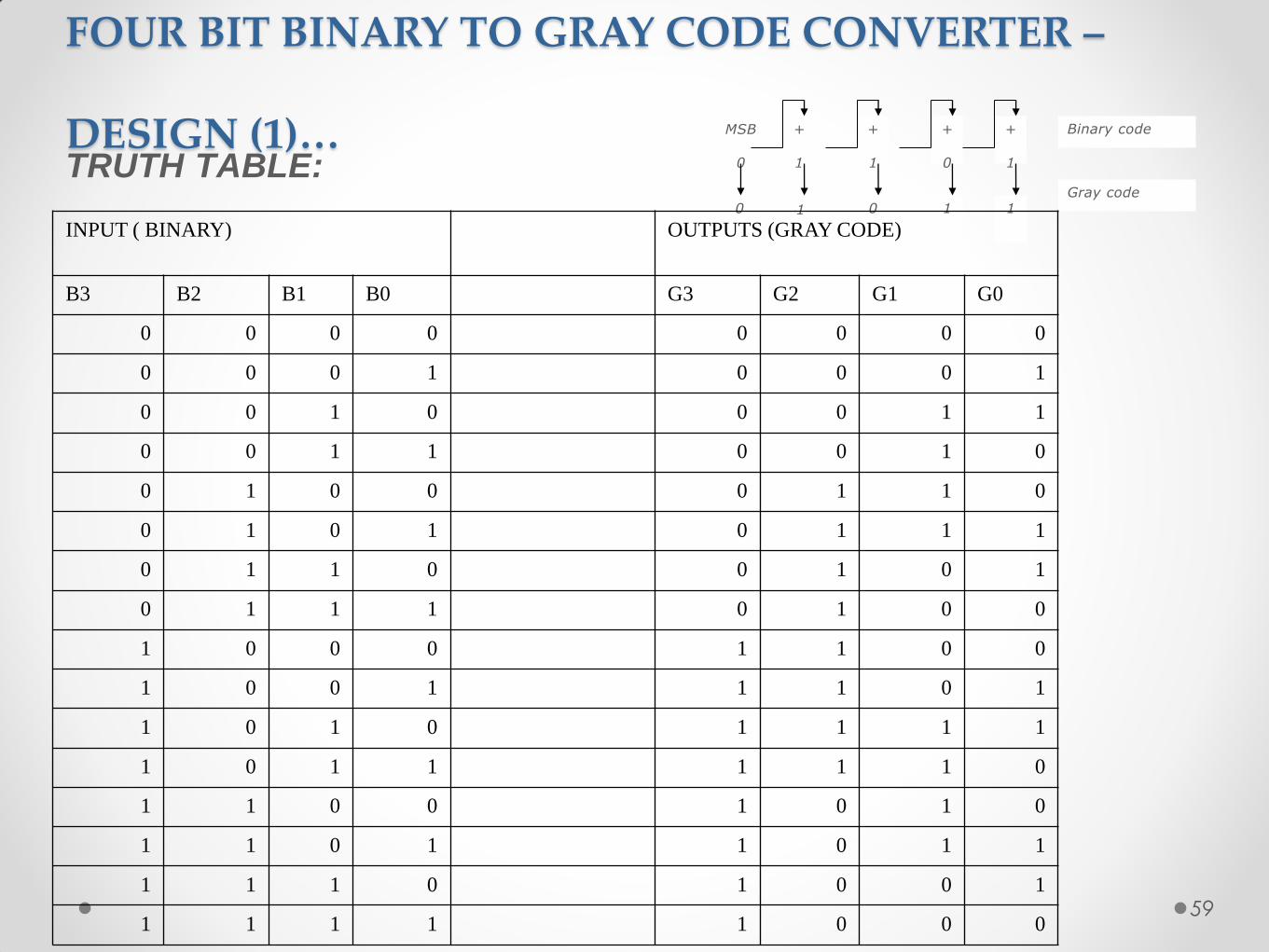
FOUR BIT BINARY TO GRAY CODE CONVERTER –
DESIGN (1)… TRUTH TABLE:
MSB
0
+
1
+
1
+
0
+
1
0 1 0 1 1
Binary code
Gray code
INPUT ( BINARY) OUTPUTS (GRAY CODE)
B3 B2 B1 B0 G3 G2 G1 G0
0 0 0 0 0 0 0 0
0 0 0 1 0 0 0 1
0 0 1 0 0 0 1 1
0 0 1 1 0 0 1 0
0 1 0 0 0 1 1 0
0 1 0 1 0 1 1 1
0 1 1 0 0 1 0 1
0 1 1 1 0 1 0 0
1 0 0 0 1 1 0 0
1 0 0 1 1 1 0 1
1 0 1 0 1 1 1 1
1 0 1 1 1 1 1 0
1 1 0 0 1 0 1 0
1 1 0 1 1 0 1 1
1 1 1 0 1 0 0 1
1 1 1 1 1 0 0 0
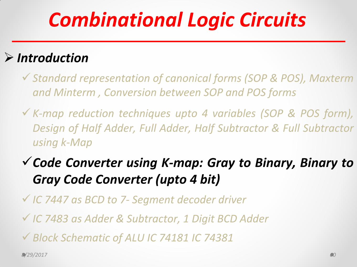
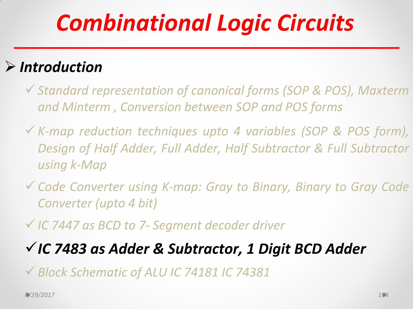
Combinational Logic Circuits
Introduction
Standard representation of canonical forms (SOP & POS), Maxterm and Minterm , Conversion between SOP and POS forms
K-map reduction techniques upto 4 variables (SOP & POS form), Design of Half Adder, Full Adder, Half Subtractor & Full Subtractor using k-Map
Code Converter using K-map: Gray to Binary, Binary to Gray Code Converter (upto 4 bit)
IC 7447 as BCD to 7- Segment decoder driver
IC 7483 as Adder & Subtractor, 1 Digit BCD Adder
Block Schematic of ALU IC 74181 IC 74381
8/29/2017 60
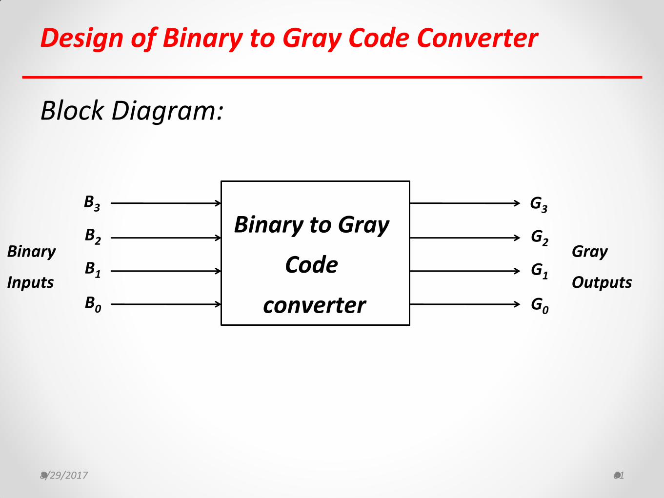
Design of Binary to Gray Code Converter
Block Diagram:
8/29/2017 61
Binary to Gray
Code
converter
B3
Binary
Inputs
Gray
Outputs
B2
B1
B0
G3
G2
G1
G0
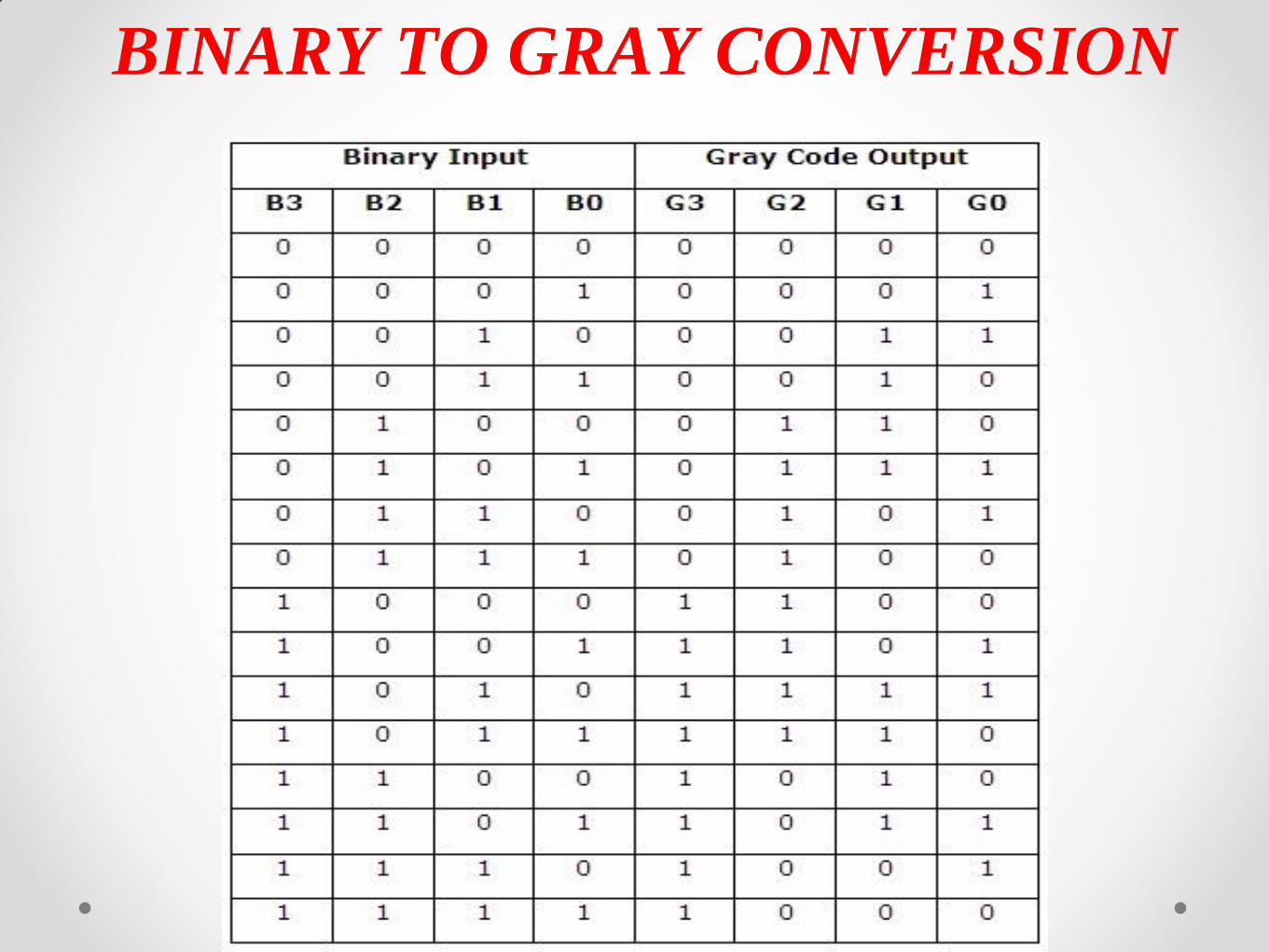
BINARY TO GRAY CONVERSION
Design of Binary to Gray Code Converter
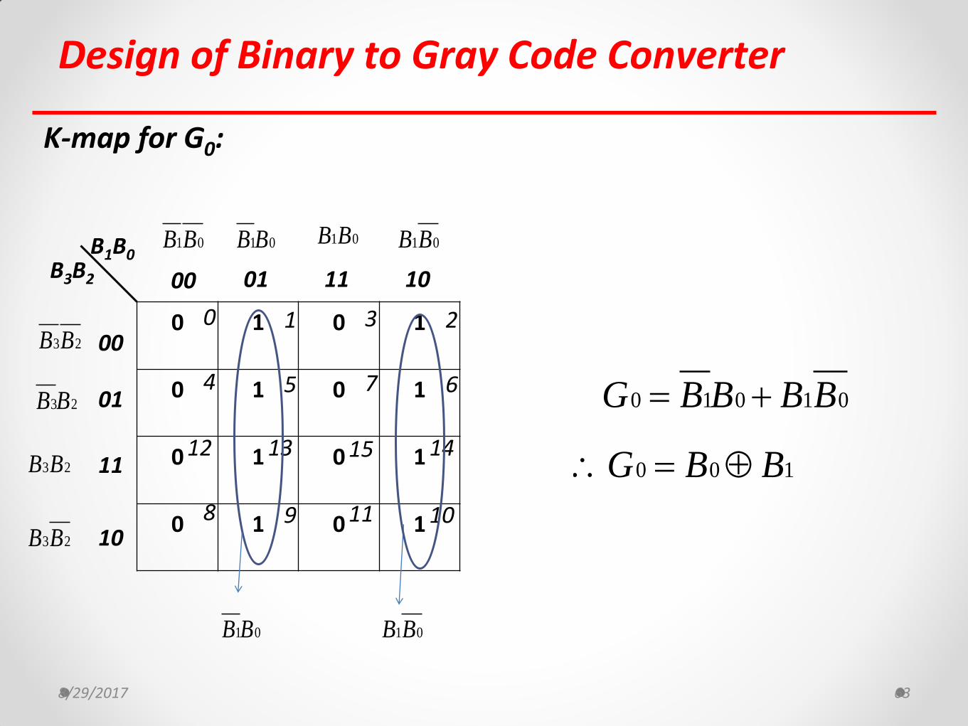
8/29/2017 63
K-map for G0:
0 1 0 1
0 1 0 1
0 1 0 1
0 1 0 1
B3B2 00 01 11 10
00
01
11
10
0 1 3 2
4 5 7 6
8 9 11 10
12 13 15 14
B1B0
3 2B B
3 2B B
3 2B B
3 2B B
1 0B B 1 0B B 1 0B B 1 0B B
1 0B B 1 0B B
0 1 0 1 0G B B B B
0 0 1G B B
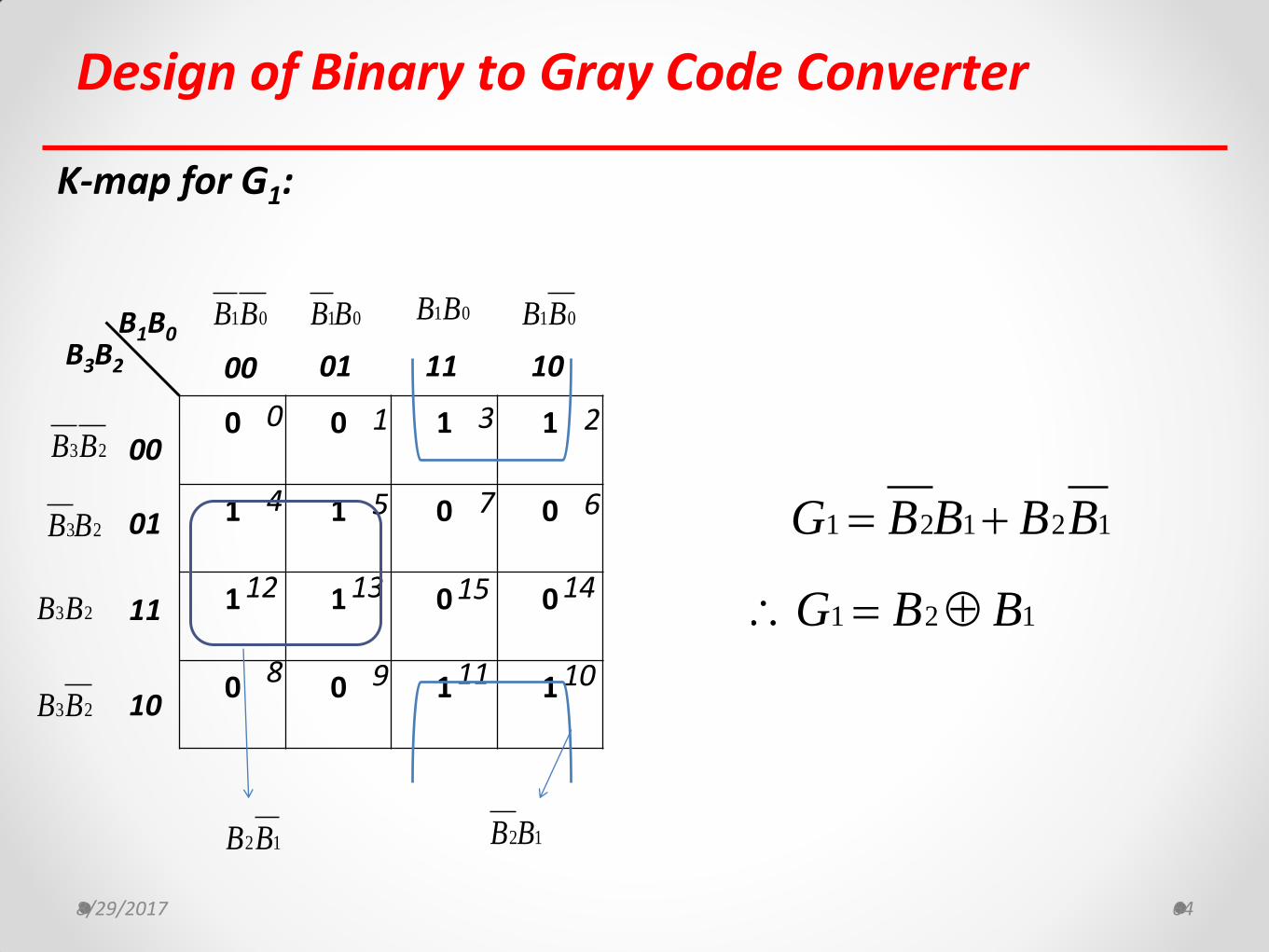
Design of Binary to Gray Code Converter
8/29/2017 64
K-map for G1:
0 0 1 1
1 1 0 0
1 1 0 0
0 0 1 1
B3B2 00 01 11 10
00
01
11
10
0 1 3 2
4 5 7 6
8 9 11 10
12 13 15 14
B1B0
3 2B B
3 2B B
3 2B B
3 2B B
1 0B B 1 0B B 1 0B B 1 0B B
2 1B B
1 2 1 2 1G B B B B
1 2 1G B B
2 1B B
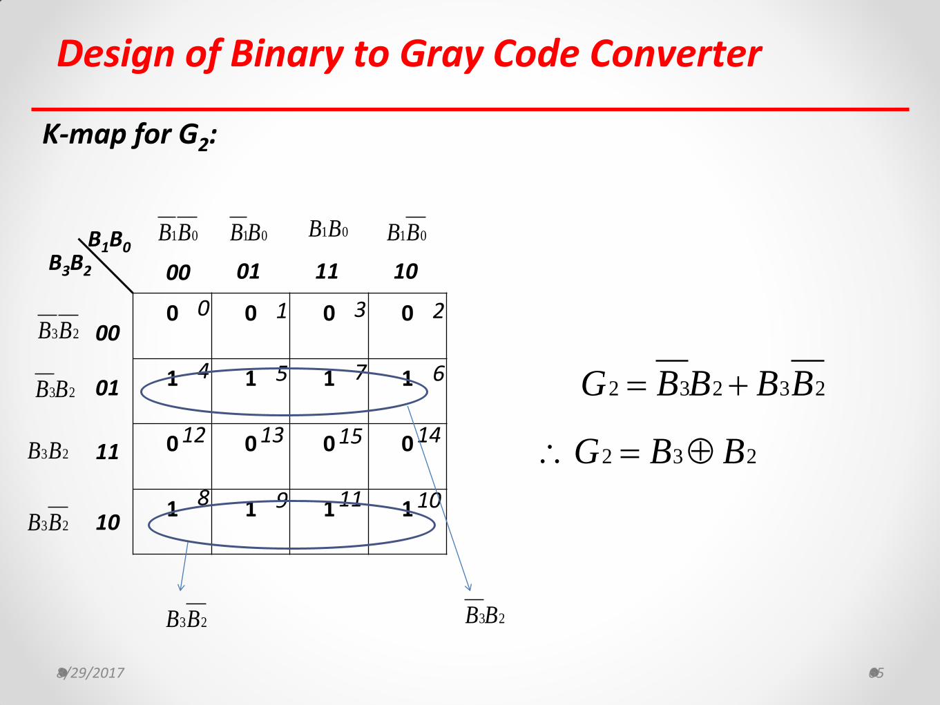
Design of Binary to Gray Code Converter
8/29/2017 65
K-map for G2:
0 0 0 0
1 1 1 1
0 0 0 0
1 1 1 1
B3B2 00 01 11 10
00
01
11
10
0 1 3 2
4 5 7 6
8 9 11 10
12 13 15 14
B1B0
3 2B B
3 2B B
3 2B B
3 2B B
1 0B B 1 0B B 1 0B B 1 0B B
3 2B B
2 3 2 3 2G B B B B
2 3 2G B B
3 2B B
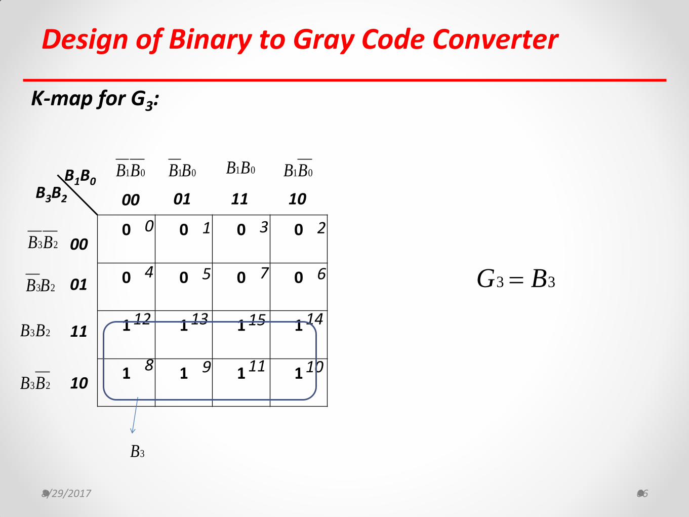
Design of Binary to Gray Code Converter
8/29/2017 66
K-map for G3:
0 0 0 0
0 0 0 0
1 1 1 1
1 1 1 1
B3B2 00 01 11 10
00
01
11
10
0 1 3 2
4 5 7 6
8 9 11 10
12 13 15 14
B1B0
3 2B B
3 2B B
3 2B B
3 2B B
1 0B B 1 0B B 1 0B B 1 0B B
3B
3 3G B
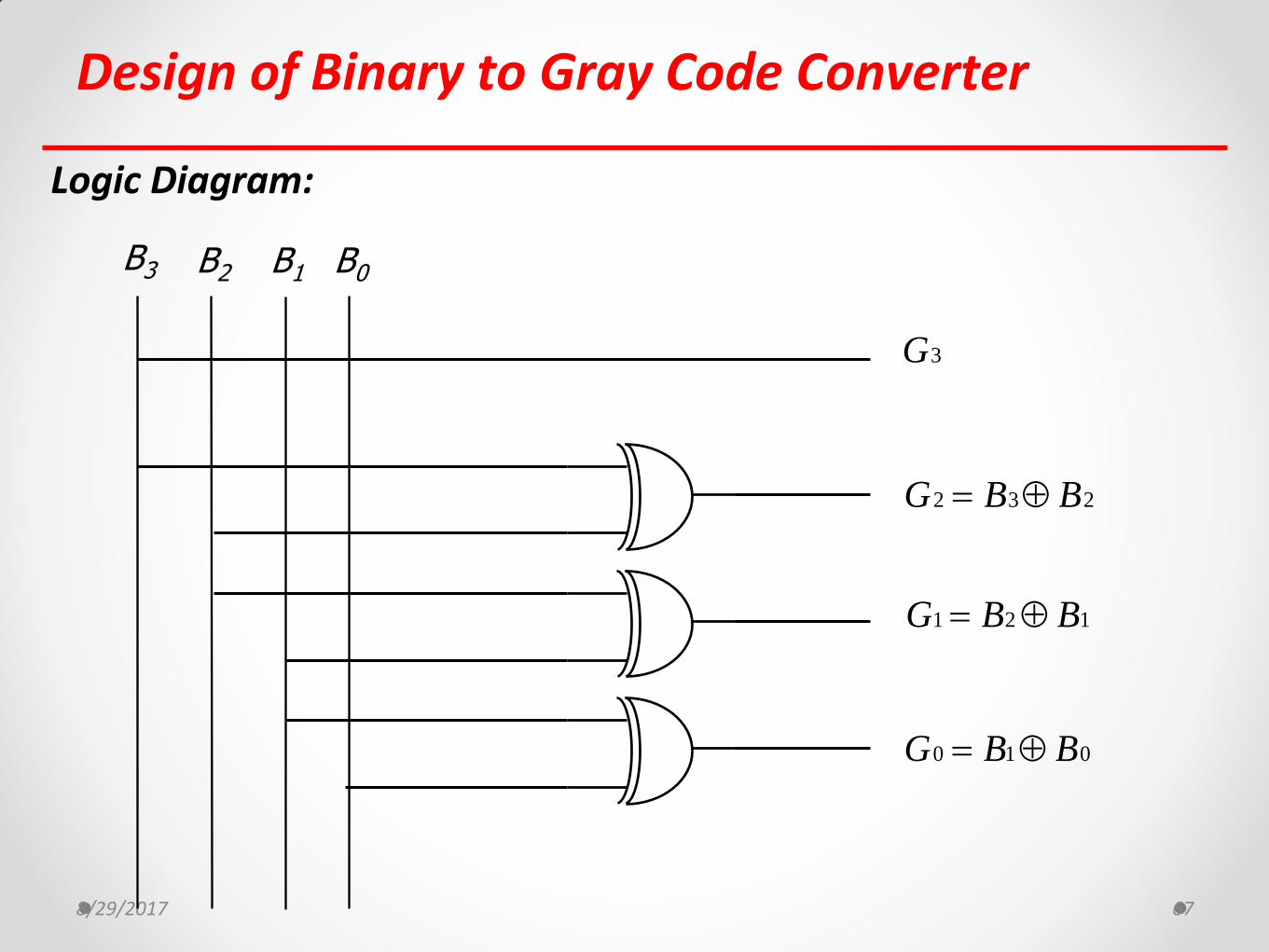
Design of Binary to Gray Code Converter
8/29/2017 67
Logic Diagram:
B3 B2 B1 B0
2 3 2G B B
1 2 1G B B
0 1 0G B B
3G
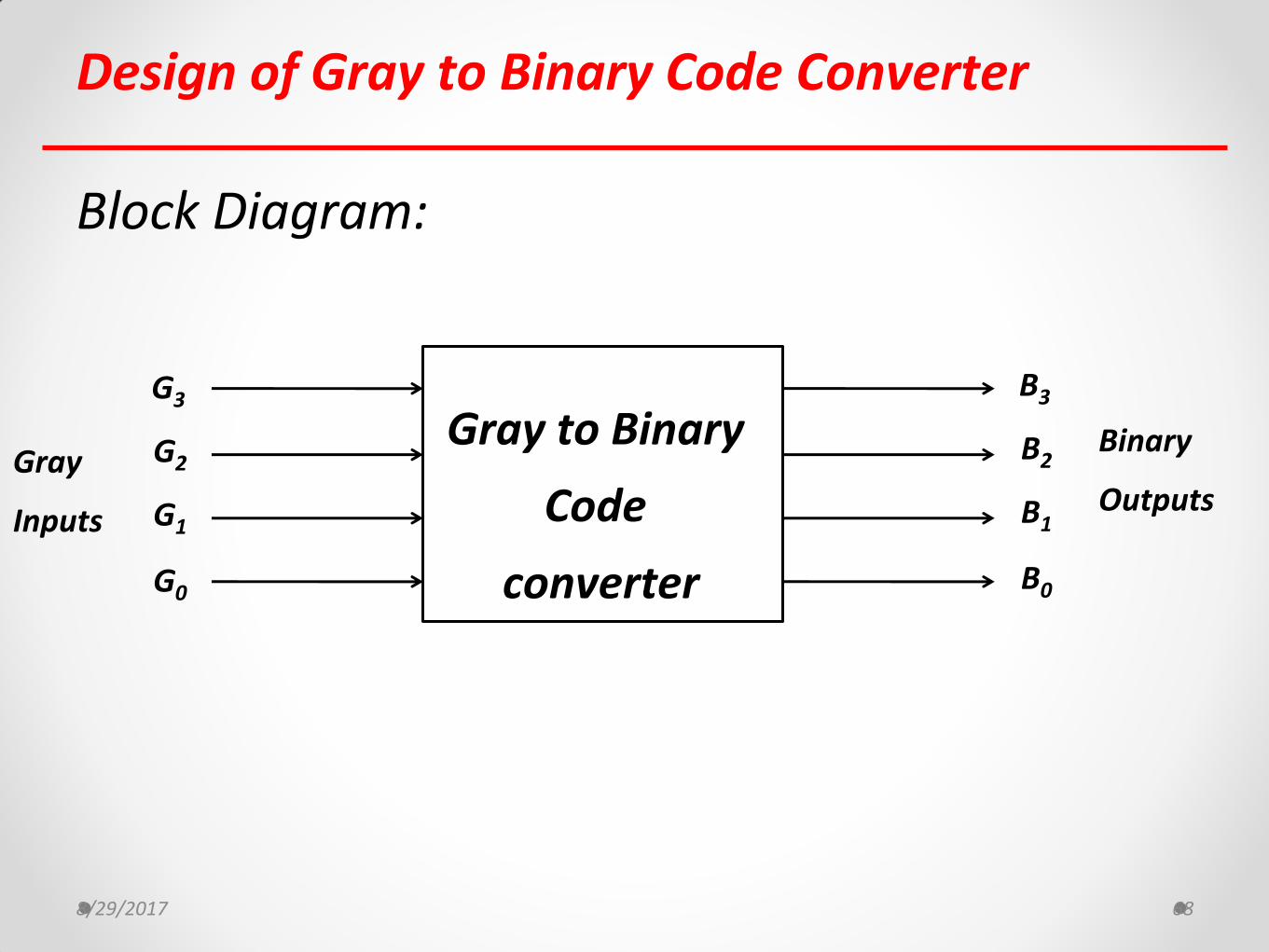
Design of Gray to Binary Code Converter
Block Diagram:
8/29/2017 68
Gray to Binary
Code
converter
B3
Binary
Outputs Gray
Inputs
B2
B1
B0
G3
G2
G1
G0
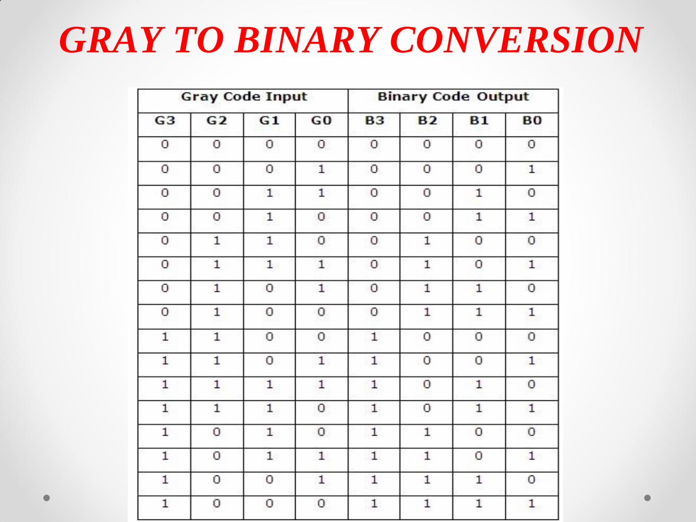
GRAY TO BINARY CONVERSION
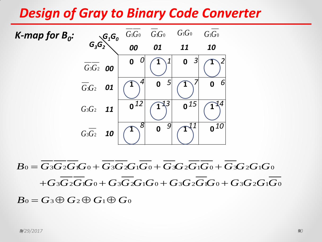
8/29/2017 70
K-map for B0:
0 1 0 1
1 0 1 0
0 1 0 1
1 0 1 0
G3G2 00 01 11 10
00
01
11
10
0 1 3 2
4 5 7 6
8 9 11 10
12 13 15 14
G1G0
Design of Gray to Binary Code Converter
3 2G G
3 2G G
3 2G G
3 2G G
1 0G G 1 0G G 1 0G G 1 0G G
0 3 2 1 0 3 2 1 0 3 2 1 0 3 2 1 0B G G G G G G G G G G G G G G G G
3 2 1 0 3 2 1 0 3 2 1 0 3 2 1 0G G G G G G G G G G G G G G G G
0 3 2 1 0B G G G G
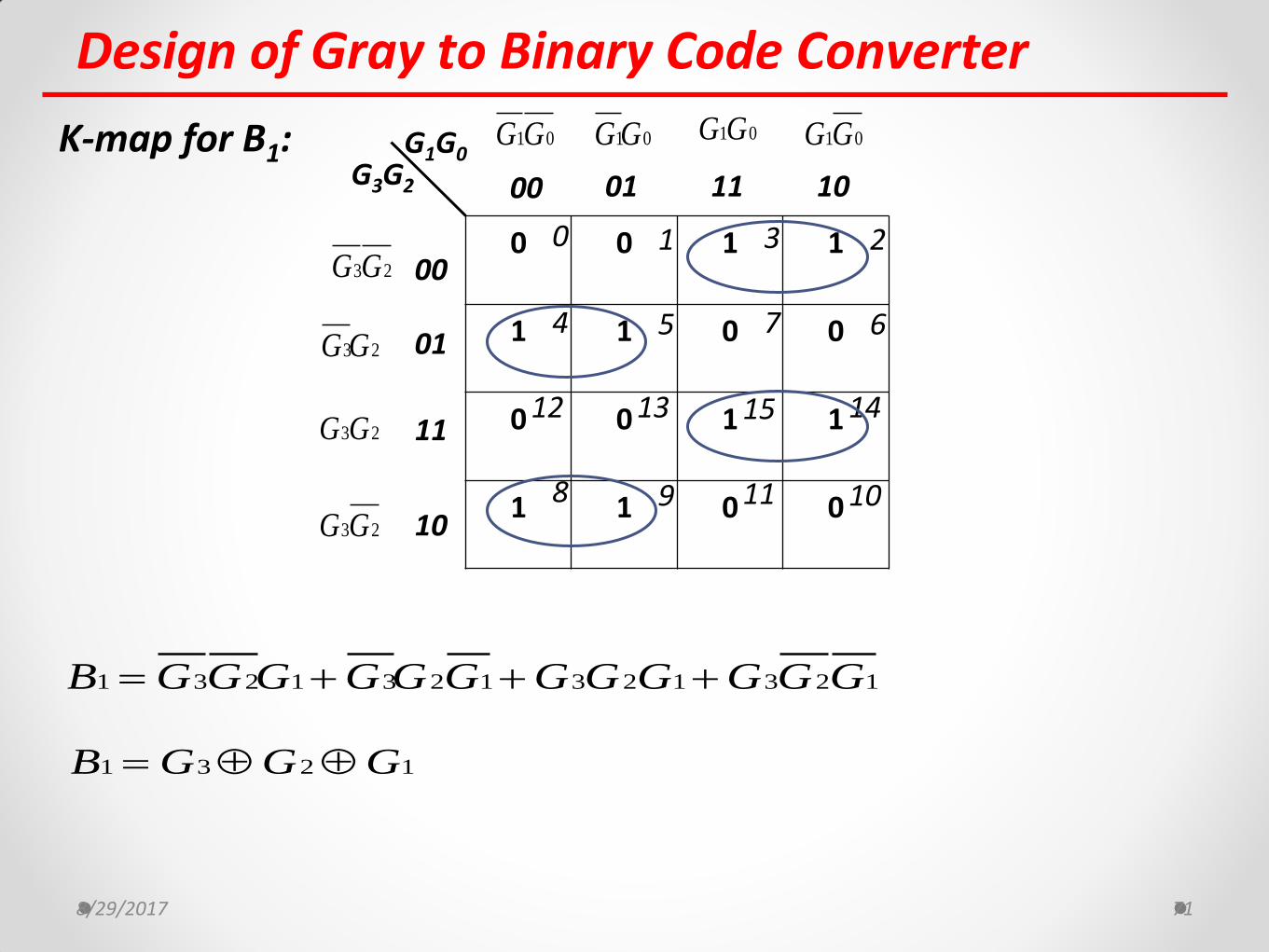
8/29/2017 71
K-map for B1:
0 0 1 1
1 1 0 0
0 0 1 1
1 1 0 0
G3G2 00 01 11 10
00
01
11
10
0 1 3 2
4 5 7 6
8 9 11 10
12 13 15 14
G1G0
Design of Gray to Binary Code Converter
3 2G G
3 2G G
3 2G G
3 2G G
1 0G G 1 0G G 1 0G G 1 0G G
1 3 2 1 3 2 1 3 2 1 3 2 1B G G G G G G G G G G G G
1 3 2 1B G G G
8/29/2017 72
K-map for B2:
0 0 0 0
1 1 1 1
0 0 0 0
1 1 1 1
G3G2 00 01 11 10
00
01
11
10
0 1 3 2
4 5 7 6
8 9 11 10
12 13 15 14
G1G0
Design of Gray to Binary Code Converter
3 2G G
3 2G G
3 2G G
3 2G G
1 0G G 1 0G G 1 0G G 1 0G G
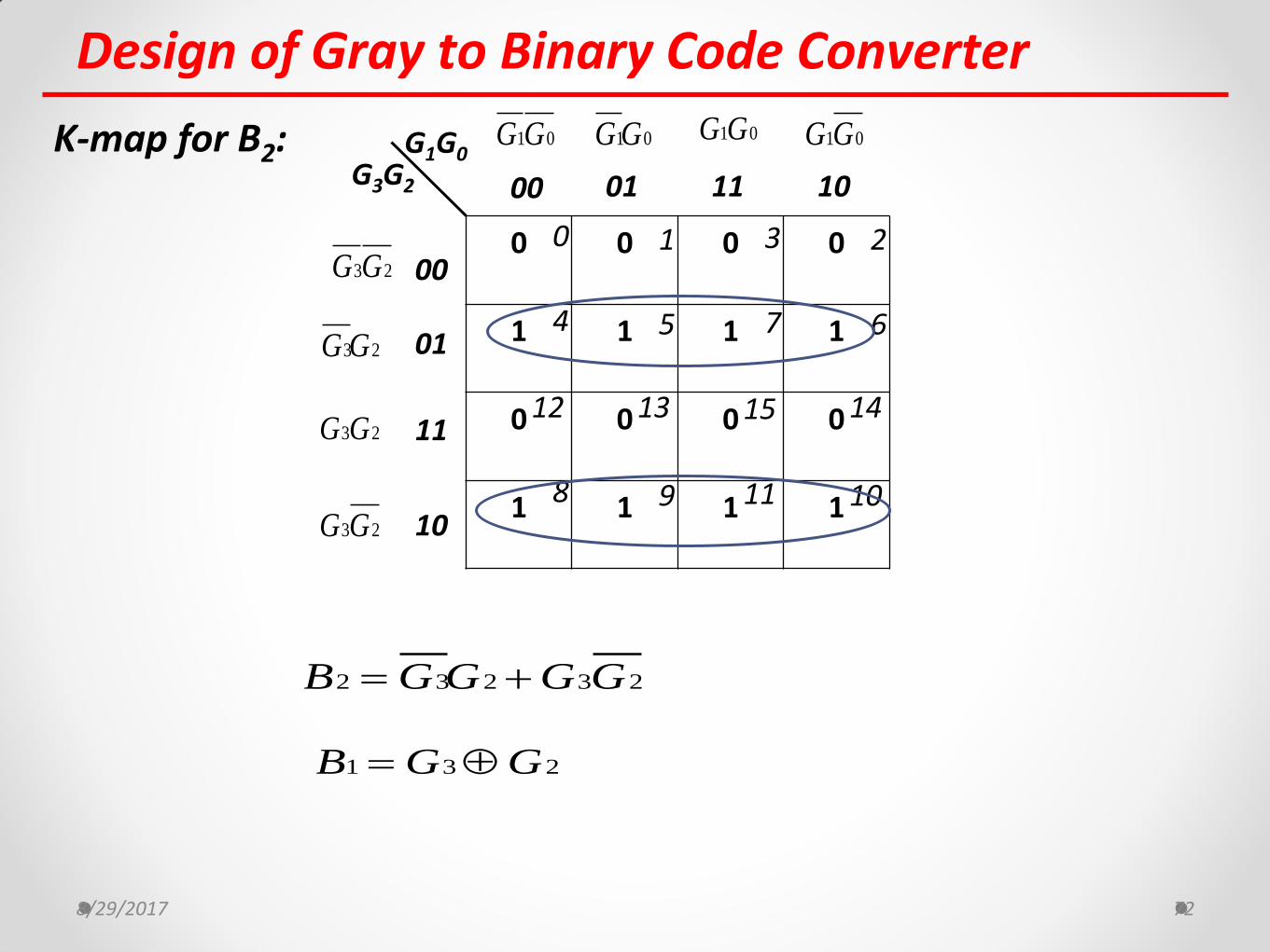
2 3 2 3 2B G G G G
1 3 2B G G
8/29/2017 73
K-map for B3:
0 0 0 0
0 0 0 0
1 1 1 1
1 1 1 1
G3G2 00 01 11 10
00
01
11
10
0 1 3 2
4 5 7 6
8 9 11 10
12 13 15 14
G1G0
Design of Gray to Binary Code Converter
3 2G G
3 2G G
3 2G G
3 2G G
1 0G G 1 0G G 1 0G G 1 0G G
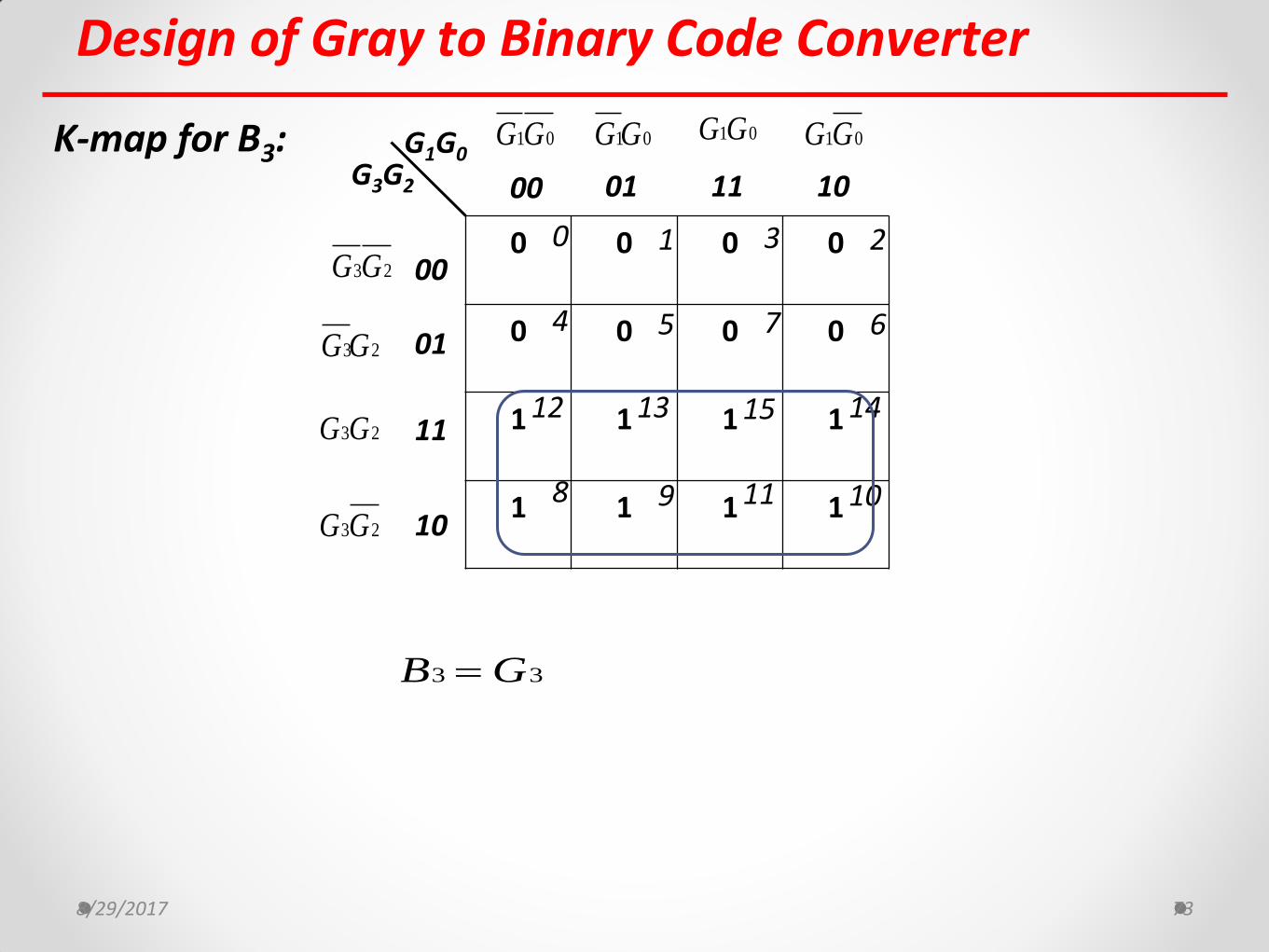
3 3B G
8/29/2017 74
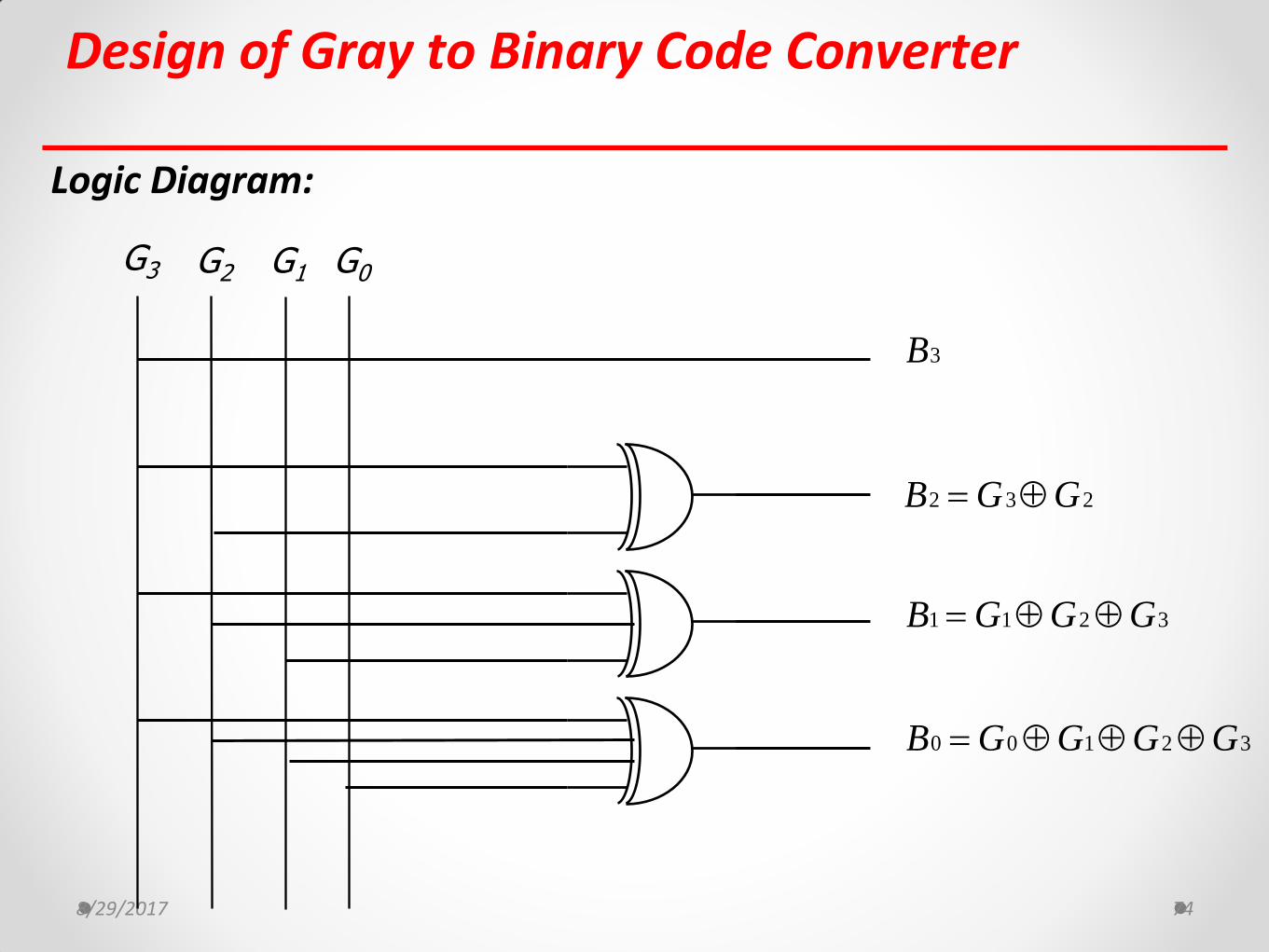
Logic Diagram:
G3 G2 G1 G0
Design of Gray to Binary Code Converter
2 3 2B G G
1 1 2 3B G G G
3B
0 0 1 2 3B G G G G
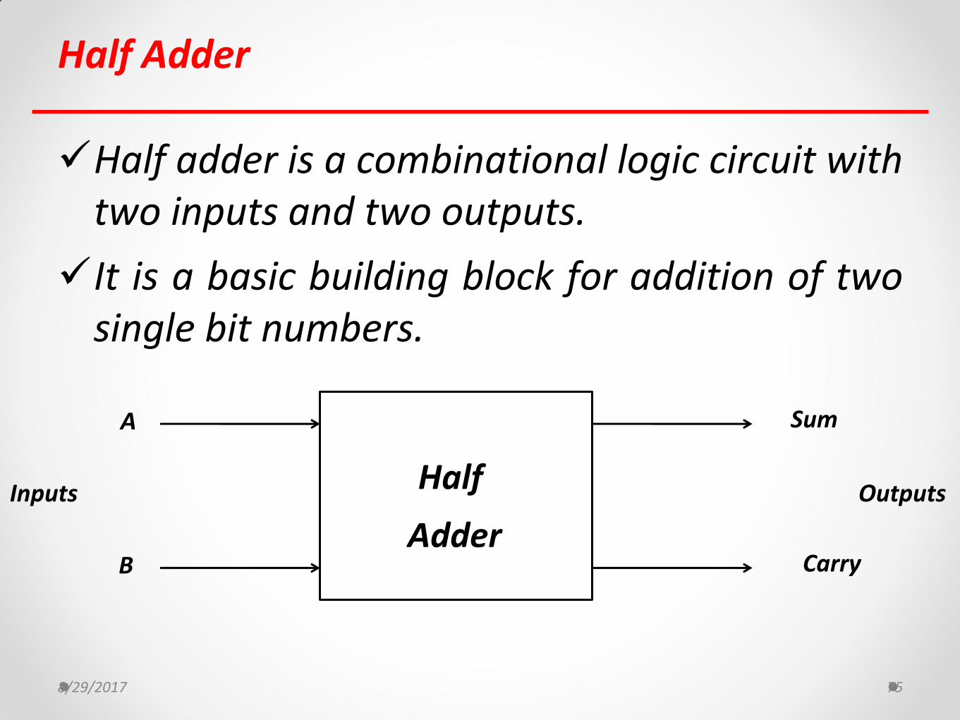
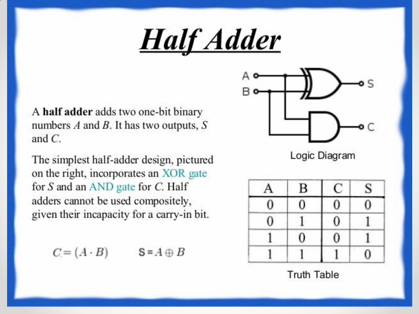
Half Adder
Half adder is a combinational logic circuit with two inputs and two outputs.
It is a basic building block for addition of two single bit numbers.
8/29/2017 75
Half
Adder
A
B
Sum
Carry
Inputs Outputs
8/29/2017 77
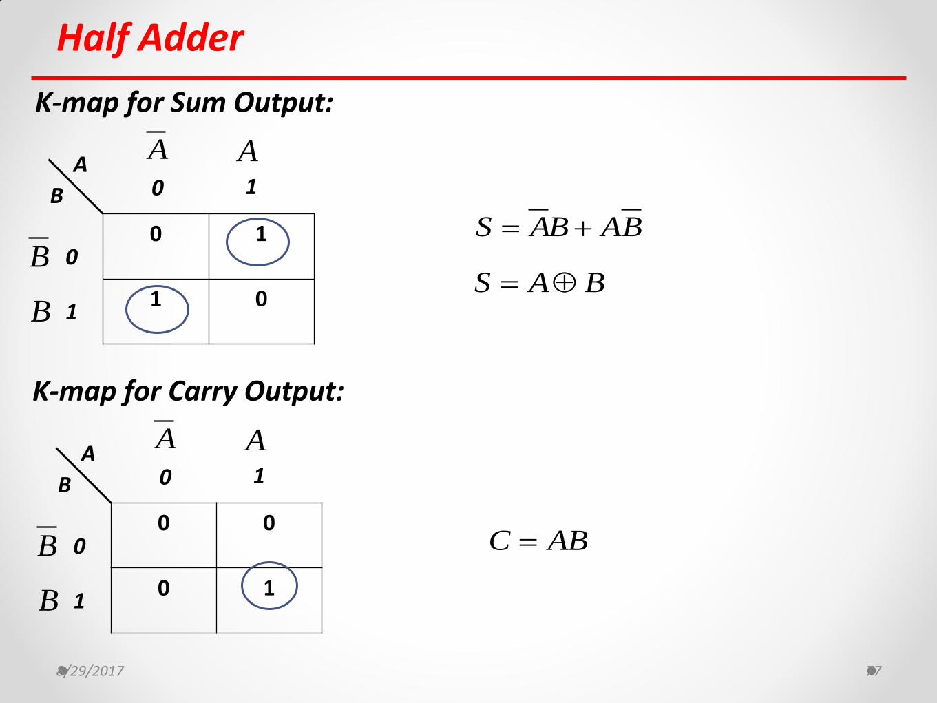
Half Adder
K-map for Sum Output:
0 1
1 0
A
B 0 1
0
1
0 0
0 1
A
B 0 1
0
1
K-map for Carry Output:
B
B
AA
B
B
AA
S AB AB
S A B
C AB
8/29/2017 78
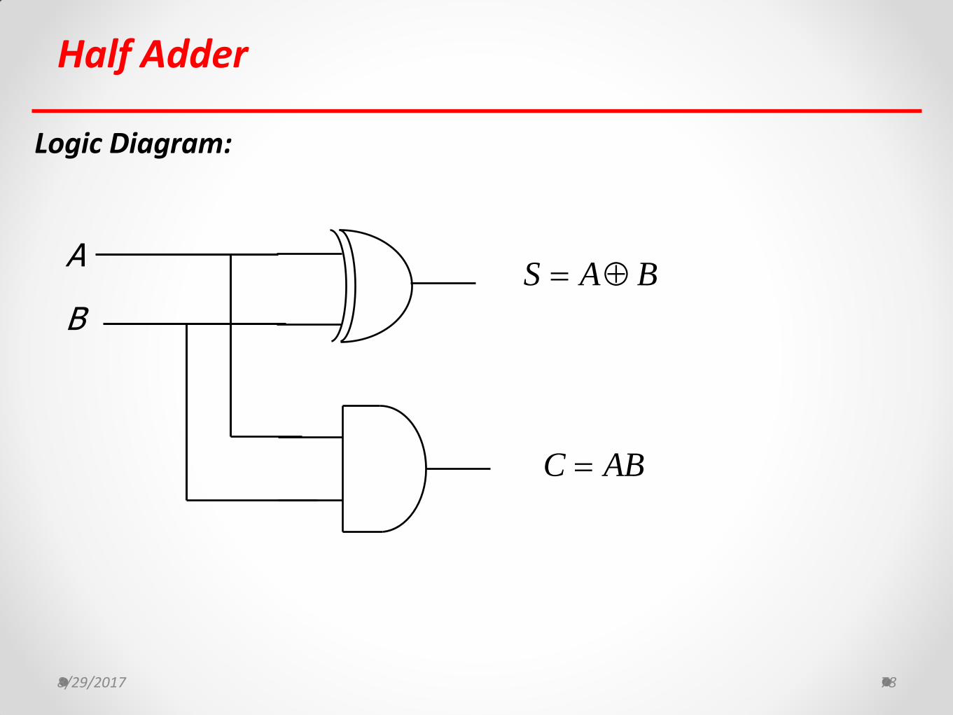
Half Adder
Logic Diagram:
A
B
S A B
C AB
8/29/2017 79
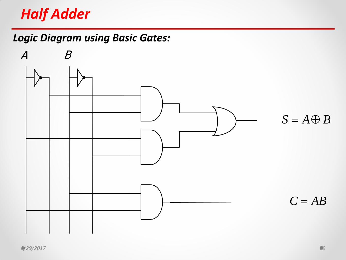
Half Adder
Logic Diagram using Basic Gates:
A B
S A B
C AB
Full Adder
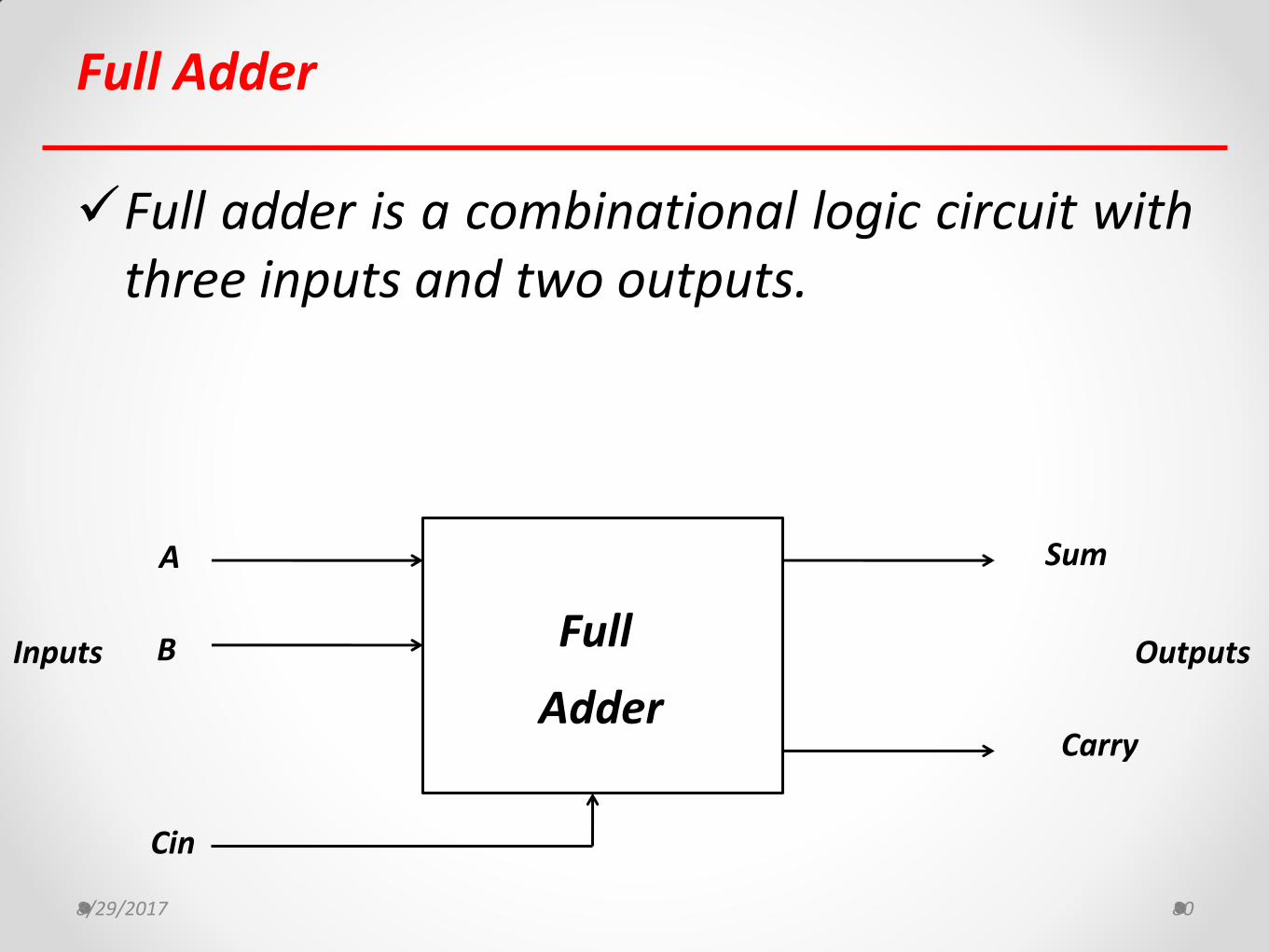
8/29/2017 80
Full adder is a combinational logic circuit with three inputs and two outputs.
Full
Adder
A
B
Sum
Carry
Inputs Outputs
Cin
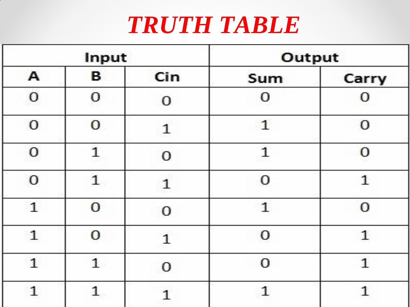
TRUTH TABLE
Full Adder
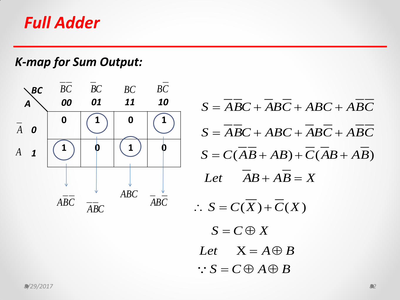
8/29/2017 82
K-map for Sum Output:
0 1 0 1
1 0 1 0
BC
A 00
0
1
01 11 10 S ABC ABC ABC ABC
BC BC BC BC
A
A
ABCABC
ABCABC
S ABC ABC ABC ABC
( ) ( )S C AB AB C AB AB
Let AB AB X
( ) ( )S C X C X
S C X
XLet A B
S C A B
Full Adder
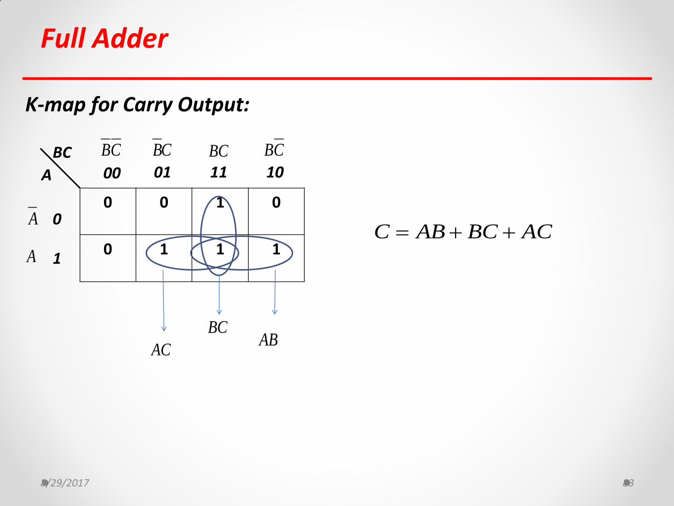
8/29/2017 83
K-map for Carry Output:
0 0 1 0
0 1 1 1
BC
A 00
0
1
01 11 10
C AB BC AC
BC BC BC BC
A
A
BCAB
AC
8/29/2017 84
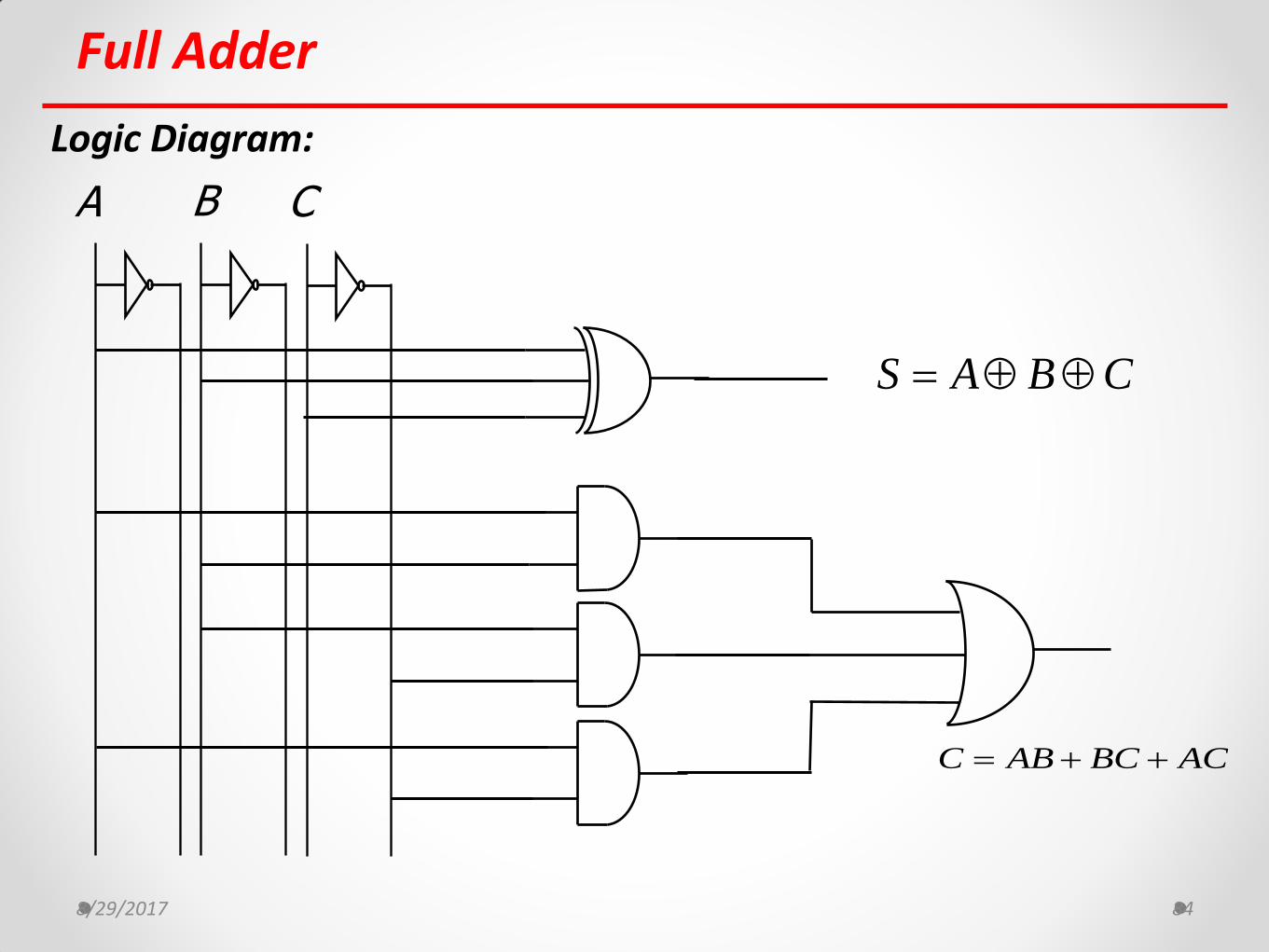
Full Adder
Logic Diagram:
A B C
S A B C
C AB BC AC
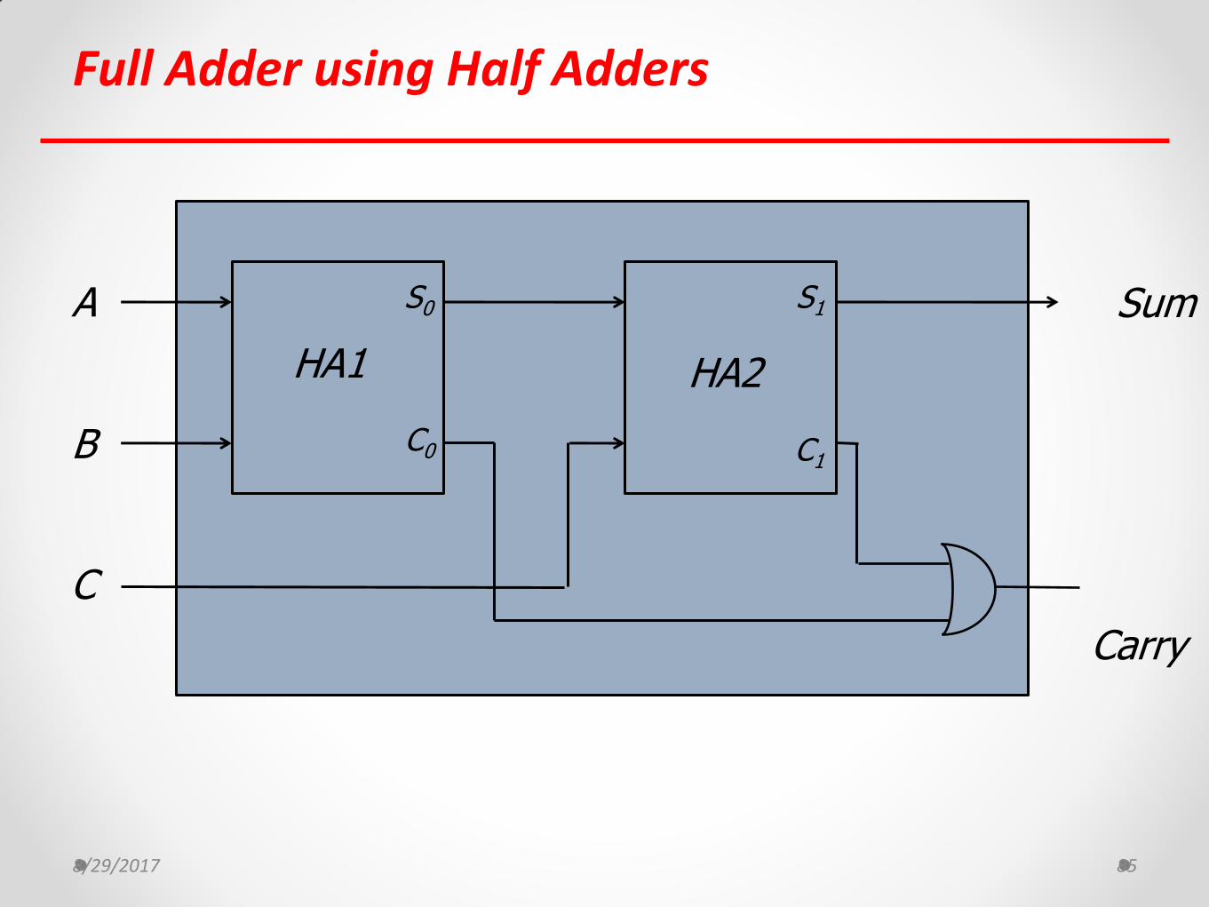
Full Adder using Half Adders
8/29/2017 85
A
B
C
HA1 HA2
S0 S1
C0 C1
Carry
Sum
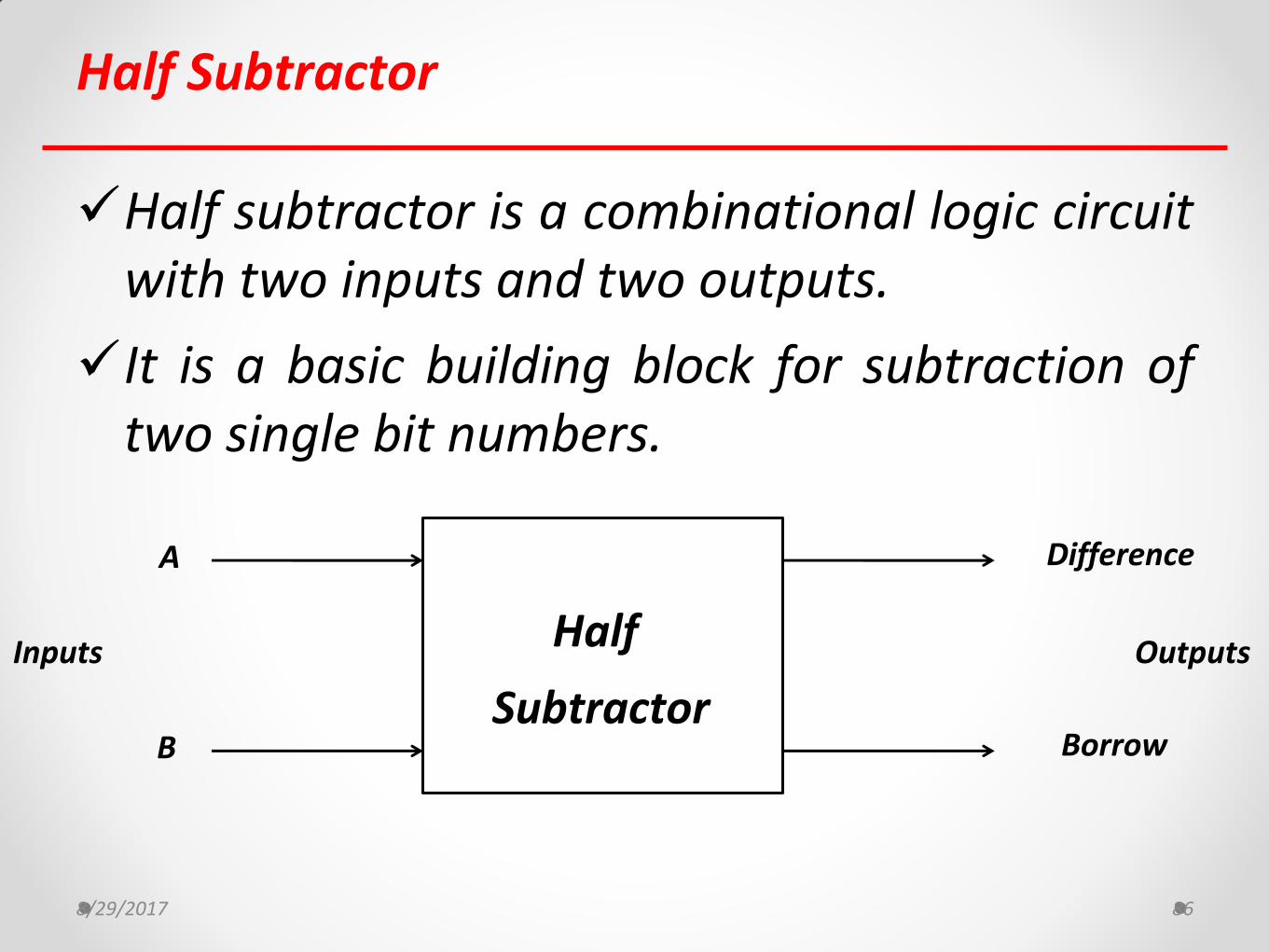
Half Subtractor
Half subtractor is a combinational logic circuit with two inputs and two outputs.
It is a basic building block for subtraction of two single bit numbers.
8/29/2017 86
Half
Subtractor
A
B
Difference
Borrow
Inputs Outputs

HALF SUBSTRACTOR
8/29/2017 88
K-map for Difference Output:
0 1
1 0
A
B 0 1
0
1
0 1
0 0
A
B 0 1
0
1
K-map for Borrow Output:
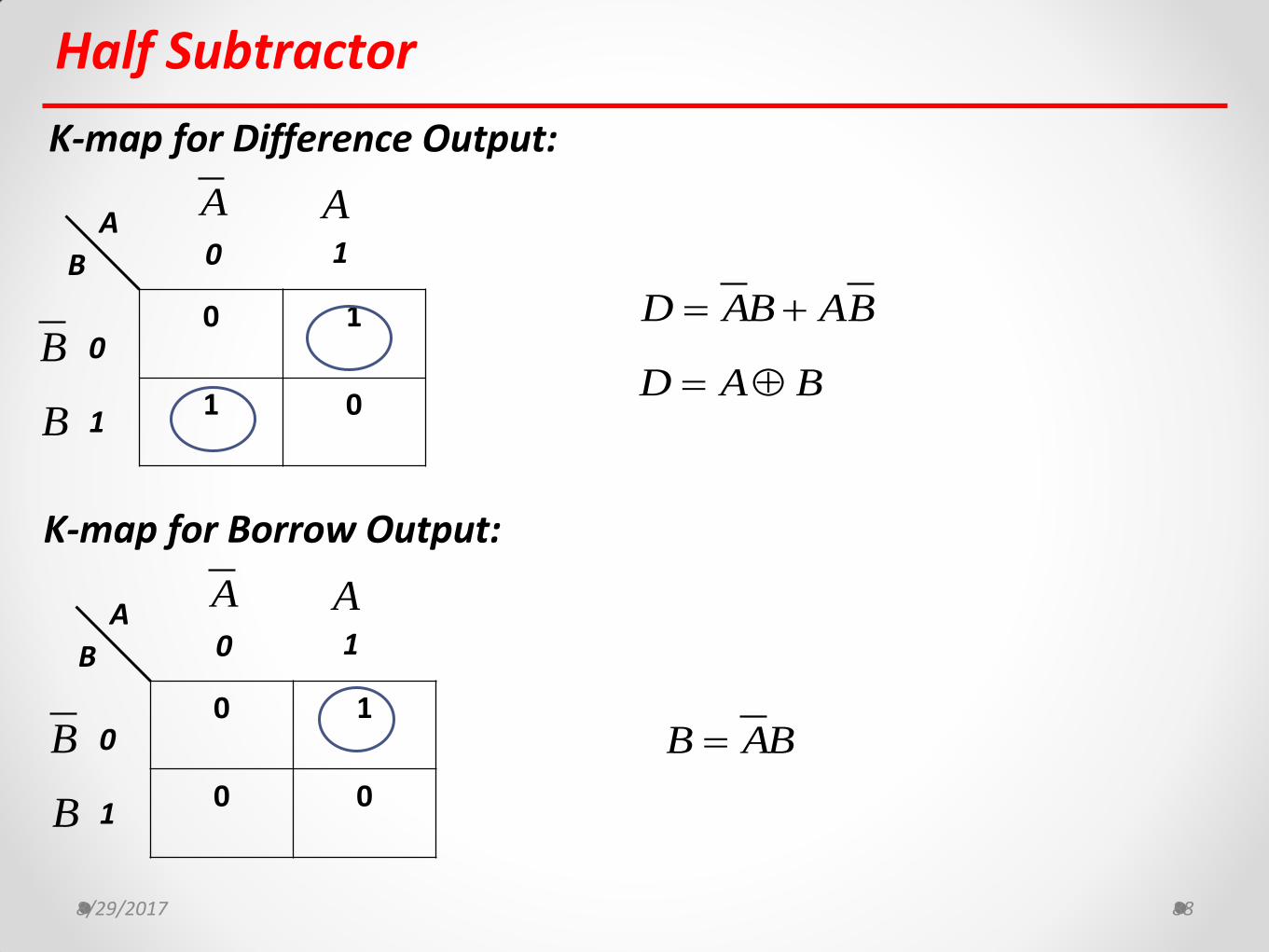
Half Subtractor
B
B
AA
B
B
AA
D AB AB
D A B
B AB
8/29/2017 89
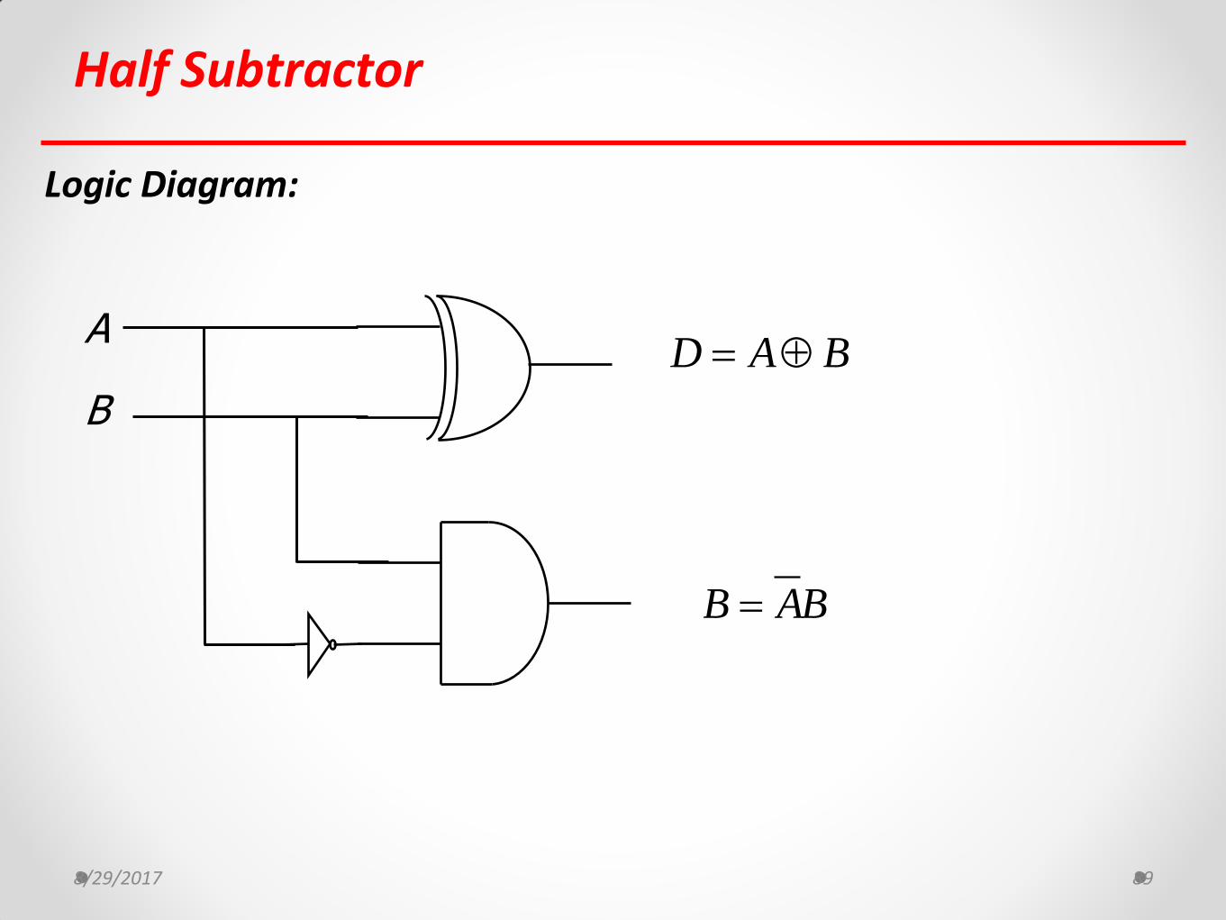
Half Subtractor
Logic Diagram:
A
B
D A B
B AB
8/29/2017 90
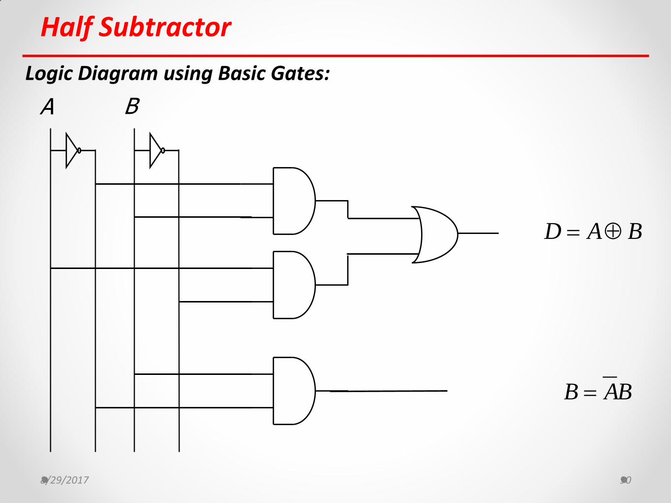
Half Subtractor
Logic Diagram using Basic Gates:
A B
D A B
B AB
Full Subtractor
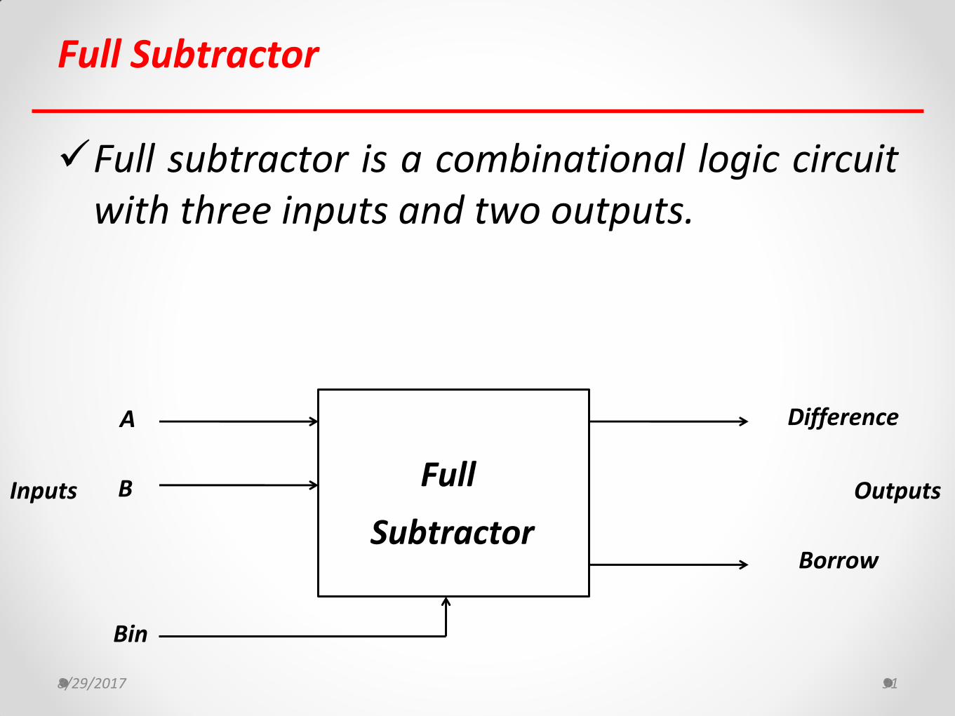
8/29/2017 91
Full subtractor is a combinational logic circuit with three inputs and two outputs.
Full
Subtractor
A
B
Difference
Borrow
Inputs Outputs
Bin

FULL SUBSTRATOR
Full Subtractor
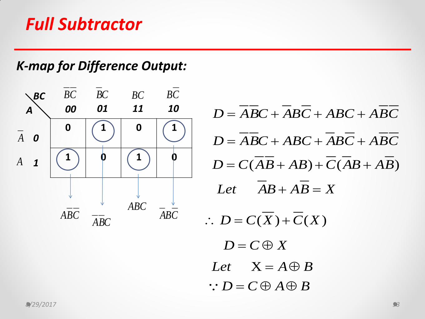
8/29/2017 93
K-map for Difference Output:
0 1 0 1
1 0 1 0
BC
A 00
0
1
01 11 10 D ABC ABC ABC ABC
BC BC BC BC
A
A
ABCABC
ABCABC
D ABC ABC ABC ABC
( ) ( )D C AB AB C AB AB
Let AB AB X
( ) ( )D C X C X
D C X
XLet A B
D C A B

Full Subtractor
8/29/2017 94
K-map for Borrow Output:
0 1 1 1
0 0 1 0
BC
A 00
0
1
01 11 10
0B AB BC AC
BC BC BC BC
A
A
BCAB
AC
8/29/2017 95
Full Subtractor
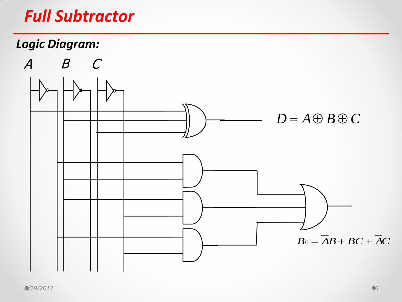
Logic Diagram:
A B C
D A B C
0B AB BC AC

Full Subtractor using Half Subtractor
8/29/2017 96
A
B
C
HS1 HS2
D0 D1
B0 B1
Borrow
Difference
Combinational Logic Circuits
Introduction
Standard representation of canonical forms (SOP & POS), Maxterm and Minterm , Conversion between SOP and POS forms
K-map reduction techniques upto 4 variables (SOP & POS form), Design of Half Adder, Full Adder, Half Subtractor & Full Subtractor using k-Map
Code Converter using K-map: Gray to Binary, Binary to Gray Code Converter (upto 4 bit)
IC 7447 as BCD to 7- Segment decoder driver
IC 7483 as Adder & Subtractor, 1 Digit BCD Adder
Block Schematic of ALU IC 74181 IC 74381
8/29/2017 97
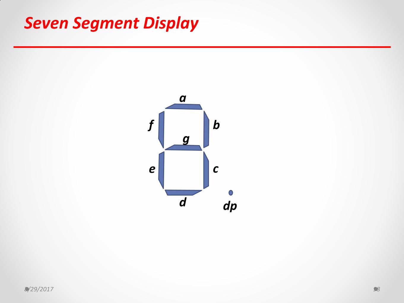
Seven Segment Display
8/29/2017 98
a
b
c
d
e
f g
dp
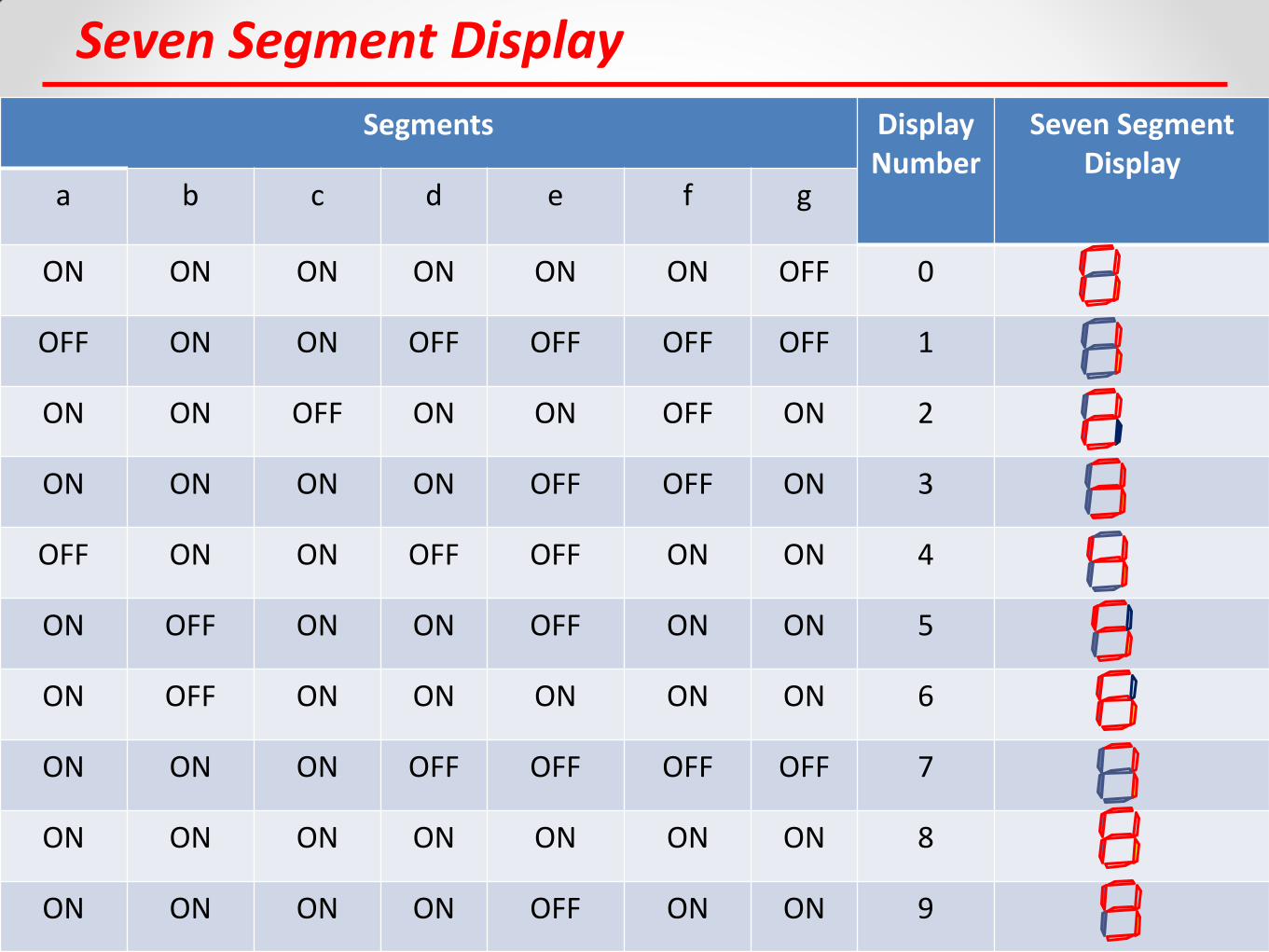
Seven Segment Display
8/29/2017 Amit Nevase 99
Segments Display Number
Seven Segment Display
a b c d e f g
ON ON ON ON ON ON OFF 0
OFF ON ON OFF OFF OFF OFF 1
ON ON OFF ON ON OFF ON 2
ON ON ON ON OFF OFF ON 3
OFF ON ON OFF OFF ON ON 4
ON OFF ON ON OFF ON ON 5
ON OFF ON ON ON ON ON 6
ON ON ON OFF OFF OFF OFF 7
ON ON ON ON ON ON ON 8
ON ON ON ON OFF ON ON 9

Types of Seven Segment Display
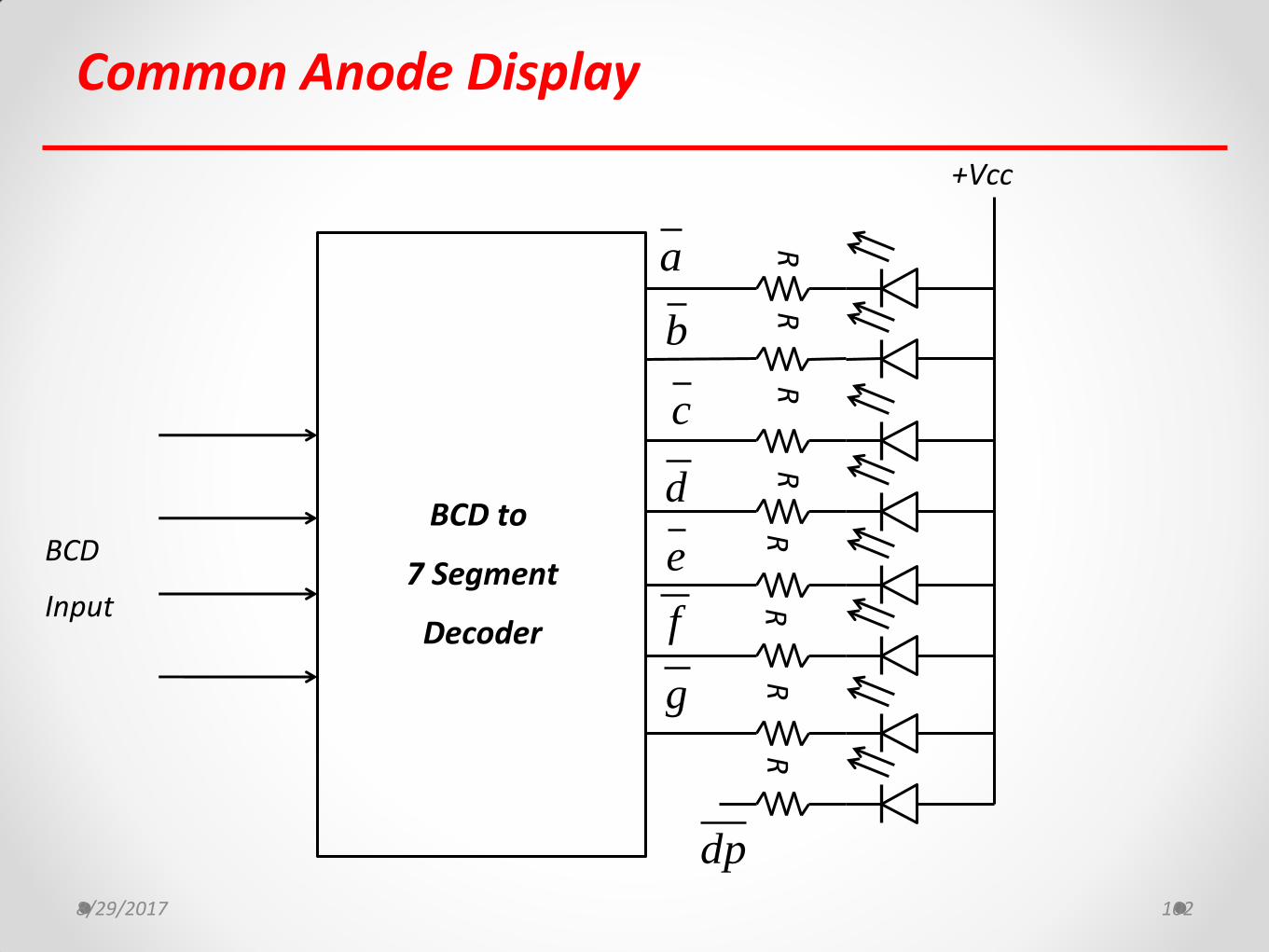
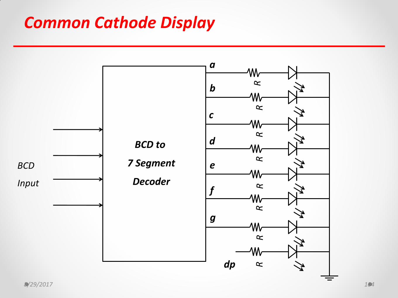
Common Cathode Display
Common Anode Display
8/29/2017 100
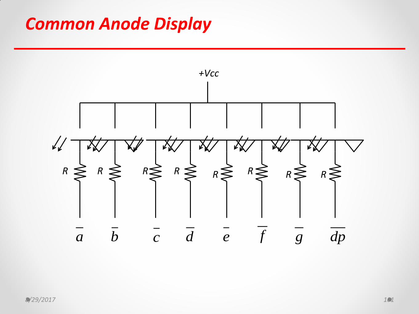
Common Anode Display
8/29/2017 101
+Vcc
R R R R R R R R
a b c d e f g dp
Common Anode Display
8/29/2017 102
+Vcc
R
R
R
R
R
R
R
R
BCD
Input
BCD to
7 Segment
Decoder
a
b
c
d
e
f
g
dp
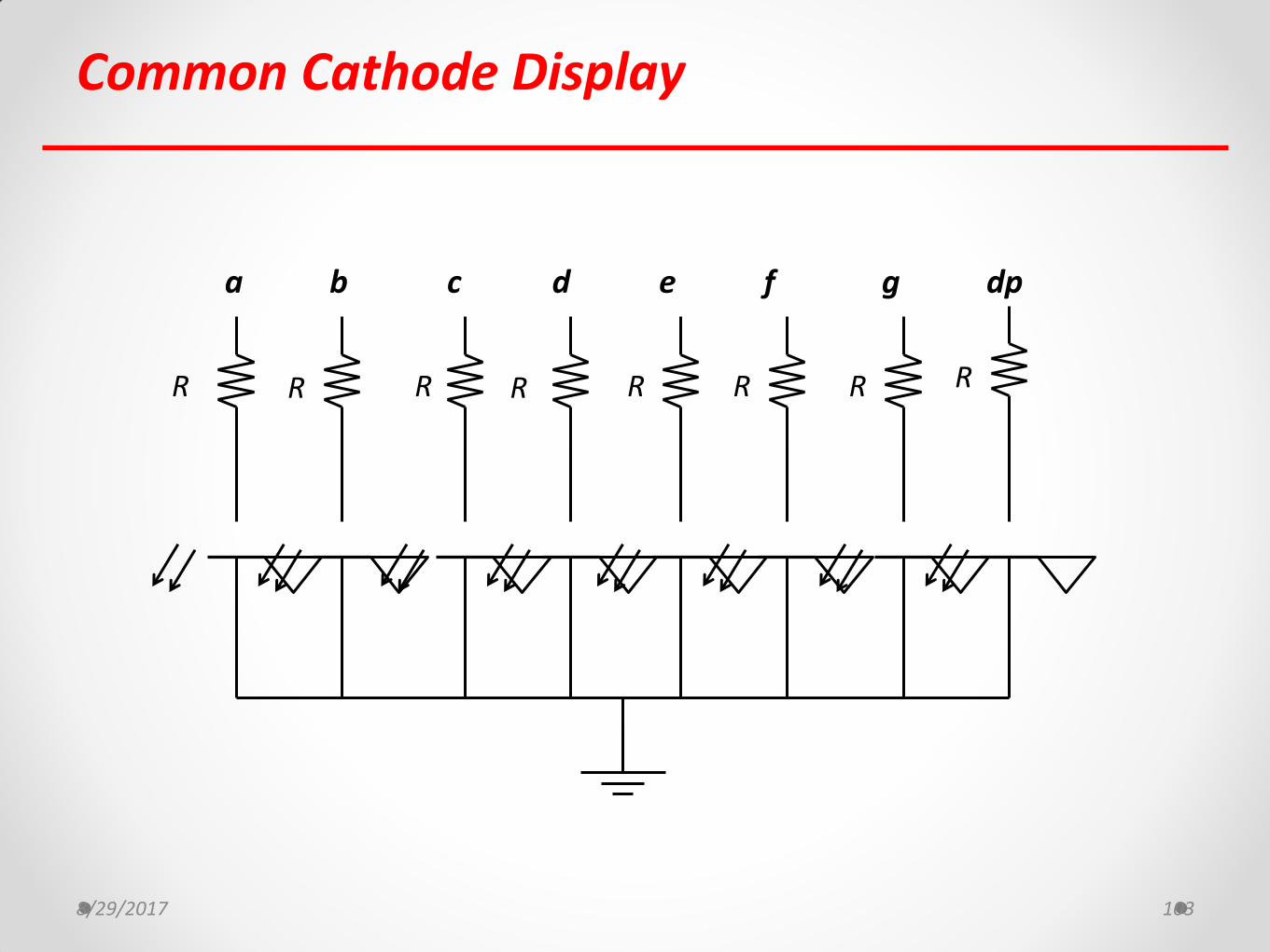
Common Cathode Display
8/29/2017 103
R R R R R R R R
a b c d e f g dp
Common Cathode Display
8/29/2017 104
BCD
Input
BCD to
7 Segment
Decoder
R
R
R
R
R
R
R
R
a
b
c
d
e
f
g
dp

BCD to 7 Segment Decoder Driver ICs
8/29/2017 105
Sr. No. IC Number Specifications
1 IC 7446, IC 74246
Active Low open collector outputs, maximum voltage 30 V, maximum current sinking capability 40mA
2 IC 7447, IC 74247
Active Low open collector outputs, maximum voltage 15 V, maximum current sinking capability 40mA
3 IC 7448, IC 74248
Active High open collector outputs, Pull up resistor 2kohm, maximum voltage 5.5 V, maximum current sinking capability 6.4mA
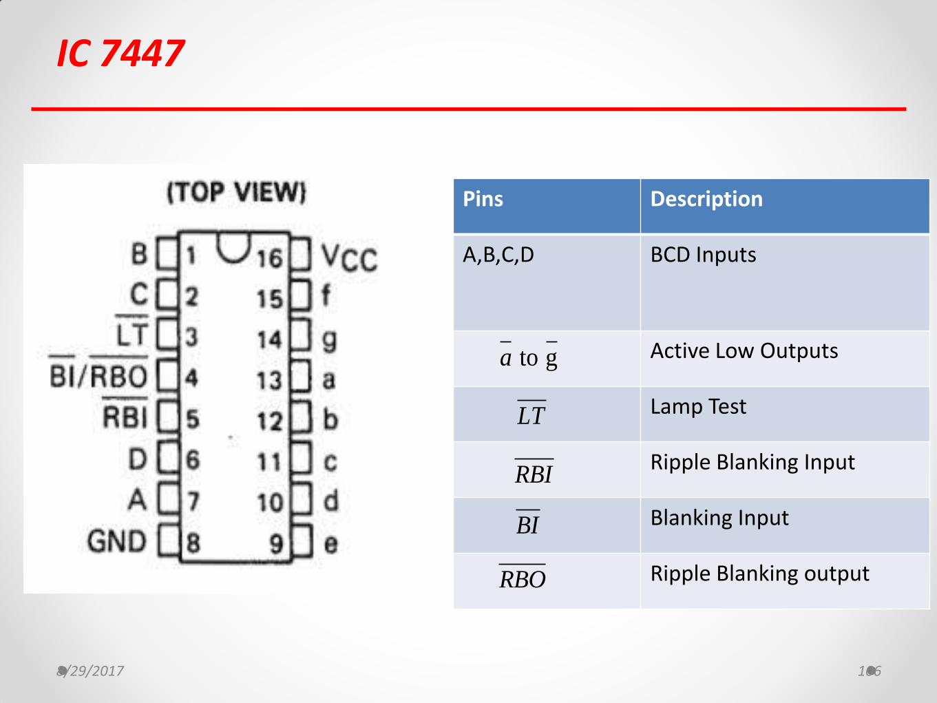
IC 7447
8/29/2017 106
Pins Description
A,B,C,D BCD Inputs
Active Low Outputs
Lamp Test
Ripple Blanking Input
Blanking Input
Ripple Blanking output
to ga
LT
RBI
BI
RBO
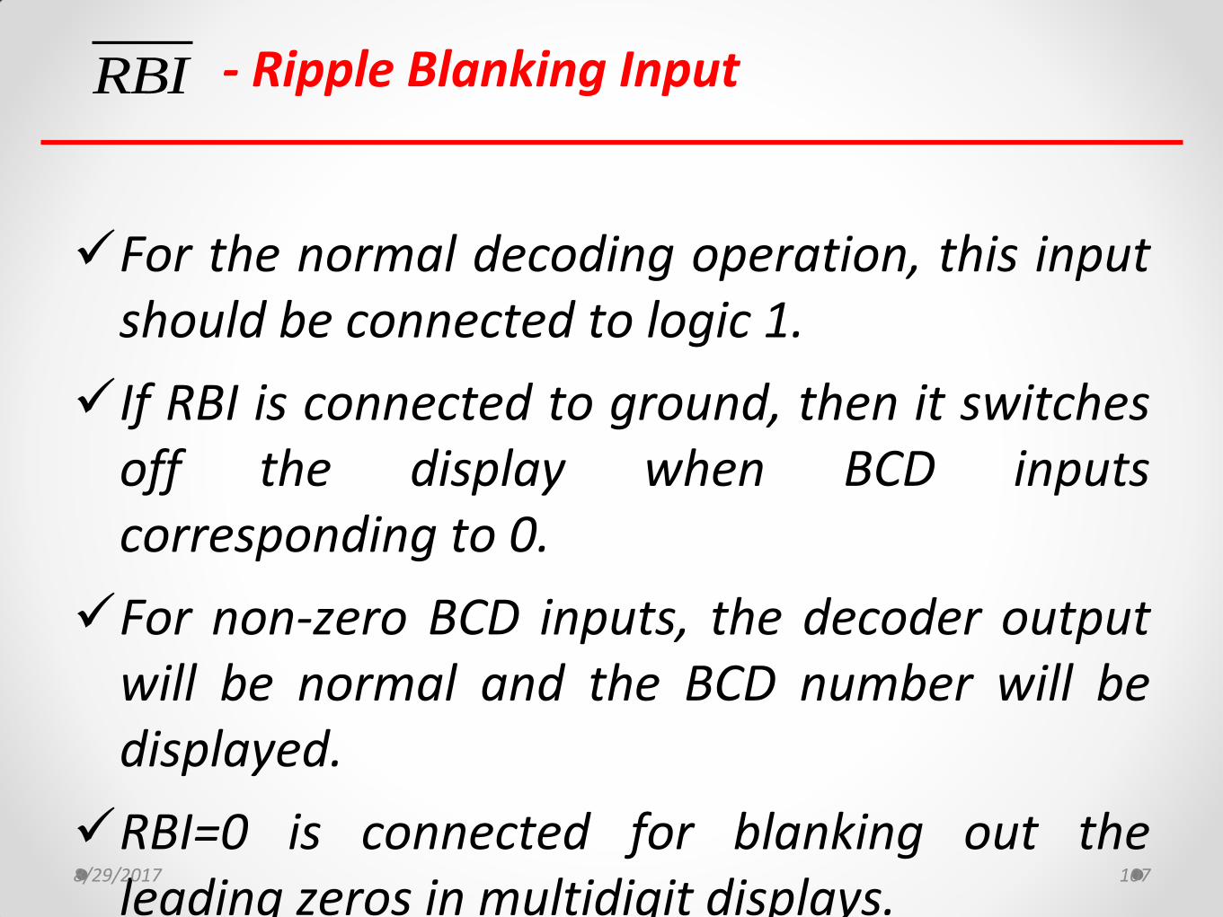
- Ripple Blanking Input
For the normal decoding operation, this input should be connected to logic 1.
If RBI is connected to ground, then it switches off the display when BCD inputs corresponding to 0.
For non-zero BCD inputs, the decoder output will be normal and the BCD number will be displayed.
RBI=0 is connected for blanking out the leading zeros in multidigit displays.
8/29/2017 107
RBI
– Blanking Input
If BI is connected to 0, then the display will be switched off irrespective of the BCD input.
This feature is used in the multiplexed display in order to save power.
In the non-multiplexed displays this input is permanently connected to Vcc
8/29/2017 108
BI
– Ripple Blanking Output
This output is normally at logic 1. But it goes to logic 0 during the zero blanking interval when RBI is forced to a low level.
RBO is used for cascading purpose and it is connected to RBI of the next stage.
8/29/2017 109
RBO
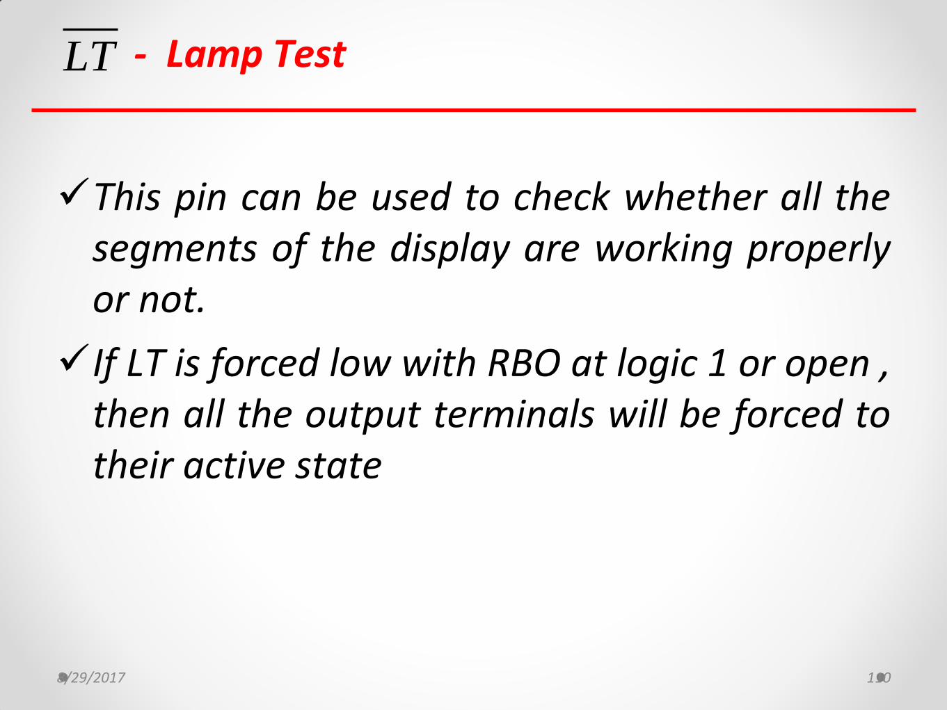
- Lamp Test
This pin can be used to check whether all the segments of the display are working properly or not.
If LT is forced low with RBO at logic 1 or open , then all the output terminals will be forced to their active state
8/29/2017 110
LT
Circuit Diagram
8/29/2017 111
a
b
c
d
e
f g
dp
R
R
R
R
R
R
R
1
2
6
7
3
5
4
13
12
11
10
9
15
14
16
8
BCD
Inputs
LSB
MSB
IC 7447
a
b
c
d
e
f
g
dp
LT
RBI
/BI RBO
Vcc
Gnd
0A
1A
2A
3A
5V
a
b
c
d
e
f
g
Common
Display Configuration – LTS 542
8/29/2017 112
a
b
c
d
e
f g
dp
a b
cde
fg
dp
Common
Common
Display Configuration
8/29/2017 113
Combinational Logic Circuits
Introduction
Standard representation of canonical forms (SOP & POS), Maxterm and Minterm , Conversion between SOP and POS forms
K-map reduction techniques upto 4 variables (SOP & POS form), Design of Half Adder, Full Adder, Half Subtractor & Full Subtractor using k-Map
Code Converter using K-map: Gray to Binary, Binary to Gray Code Converter (upto 4 bit)
IC 7447 as BCD to 7- Segment decoder driver
IC 7483 as Adder & Subtractor, 1 Digit BCD Adder
Block Schematic of ALU IC 74181 IC 74381
8/29/2017 114
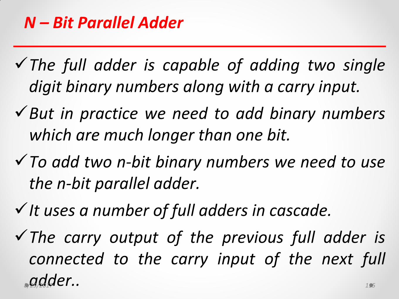
N – Bit Parallel Adder
The full adder is capable of adding two single digit binary numbers along with a carry input.
But in practice we need to add binary numbers which are much longer than one bit.
To add two n-bit binary numbers we need to use the n-bit parallel adder.
It uses a number of full adders in cascade.
The carry output of the previous full adder is connected to the carry input of the next full adder.. 8/29/2017 115
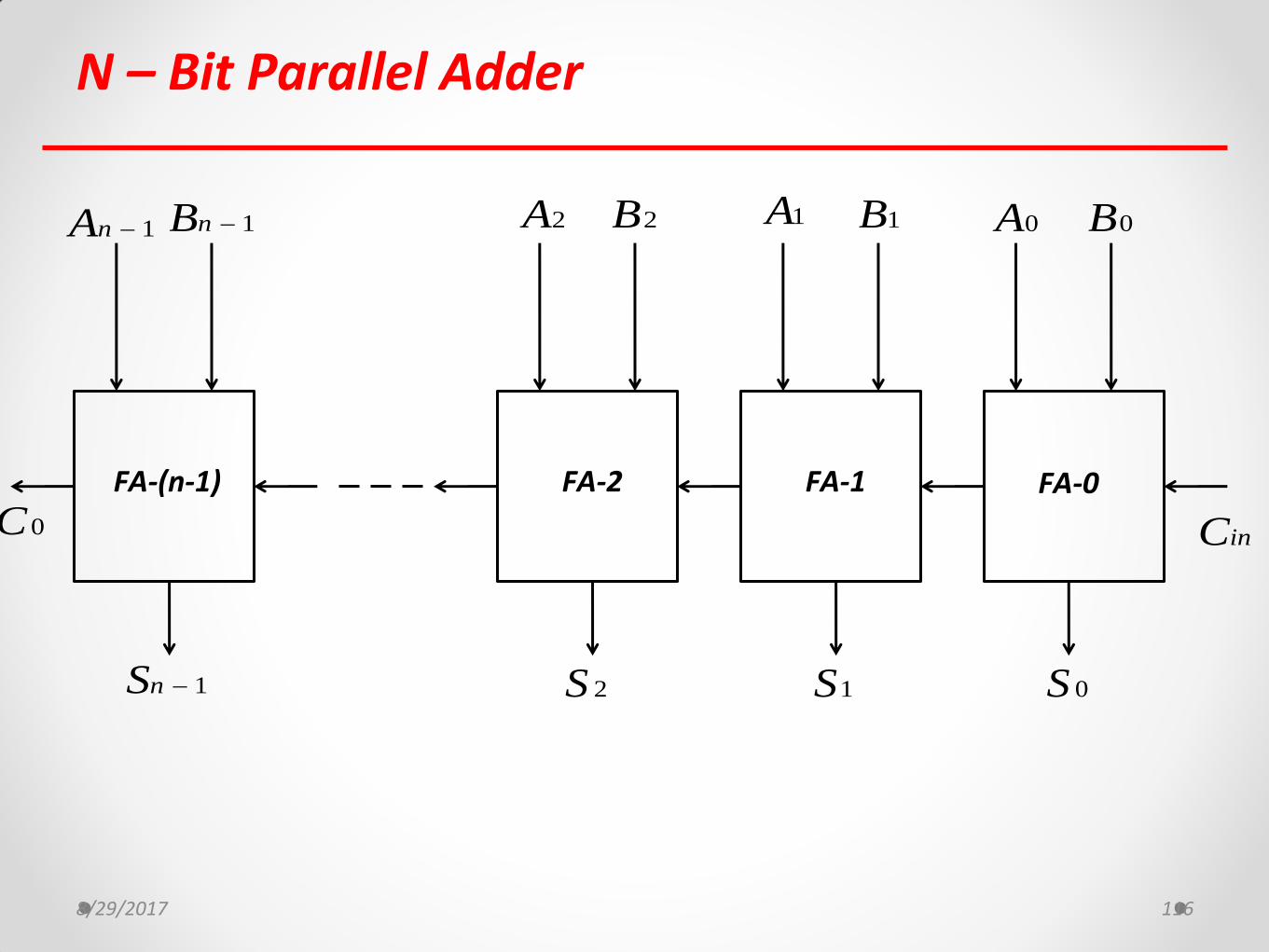
N – Bit Parallel Adder
8/29/2017 116
FA-0 FA-1 FA-2 FA-(n-1)
0A1A2A1nA 0B1B2B1nB
0S1S2S1nS
0C inC
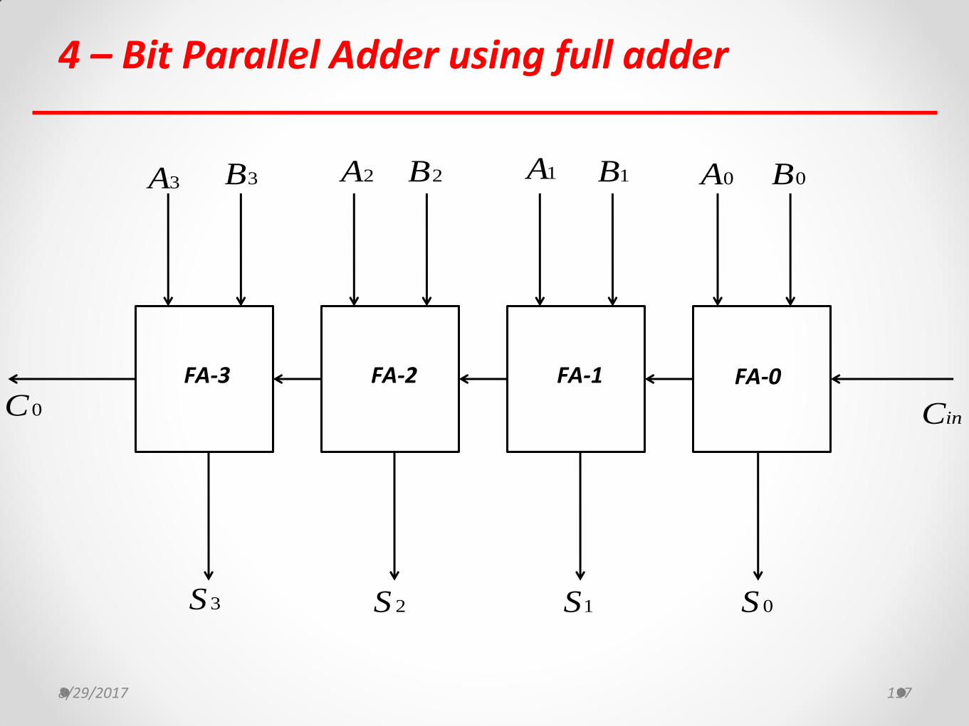
4 – Bit Parallel Adder using full adder
8/29/2017 117
FA-0 FA-1 FA-2 FA-3
0A1A2A3A 0B1B2B3B
0S1S2S3S
0C inC
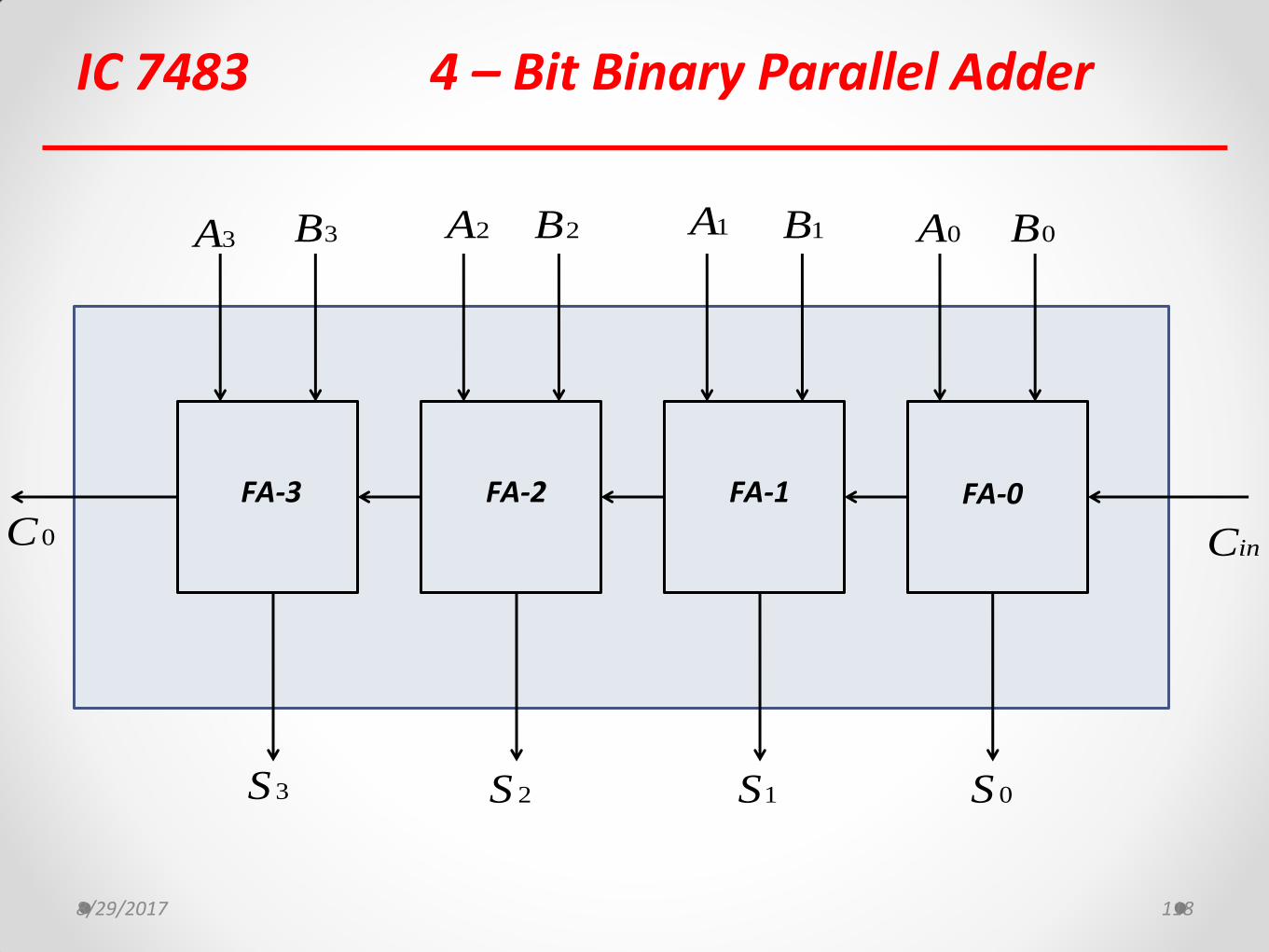
IC 7483 4 – Bit Binary Parallel Adder
8/29/2017 118
FA-0 FA-1 FA-2 FA-3
0A1A2A3A 0B1B2B3B
0S1S2S3S
0C inC
IC 7483 4 – Bit Binary Parallel Adder
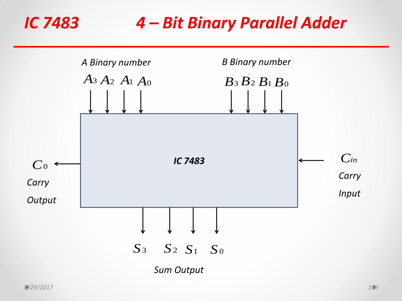
8/29/2017 119
Sum Output
IC 7483
Carry
Output
Carry
Input
A Binary number B Binary number
0A1A2A3A 0B1B2B3B
0S1S2S3S
0CinC
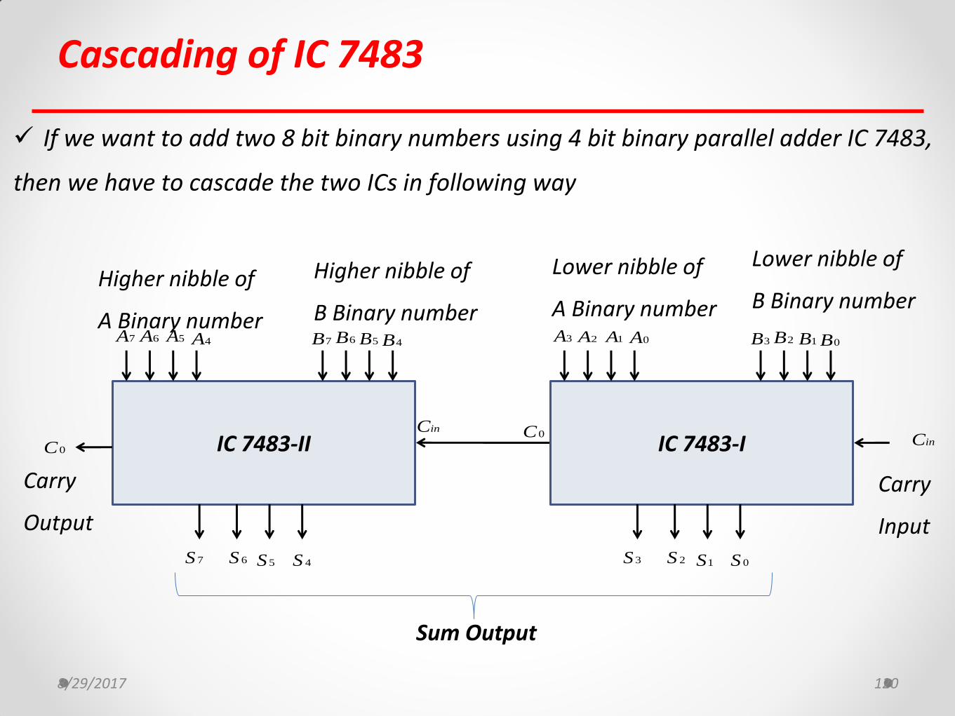
Cascading of IC 7483
8/29/2017 120
IC 7483-II
Carry
Output
Higher nibble of
A Binary number
Higher nibble of
B Binary number
Sum Output
IC 7483-I
Carry
Input
Lower nibble of
A Binary number
Lower nibble of
B Binary number
If we want to add two 8 bit binary numbers using 4 bit binary parallel adder IC 7483,
then we have to cascade the two ICs in following way
4A5A6A7A 4B5B6B7B
4S5S6S7S
0C
inC
0A1A2A3A 0B1B2B3B
0S1S2S3S
0CinC
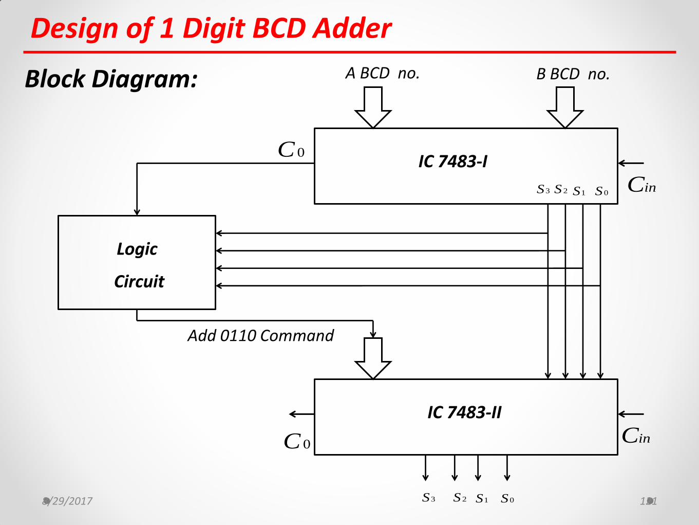
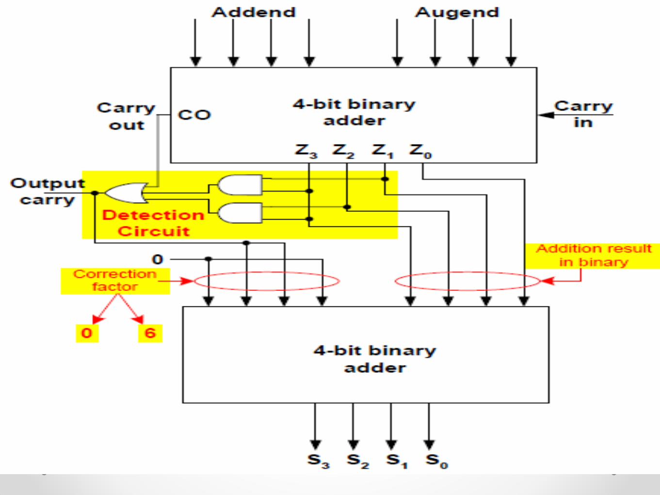
Design of 1 Digit BCD Adder
Block Diagram:
8/29/2017 121
Logic
Circuit
IC 7483-I
IC 7483-II
Add 0110 Command
A BCD no. B BCD no.
inC
0C
inC0C
3S 2S 1S 0S
3S 2S 1S 0S
Design of 1 Digit BCD Adder
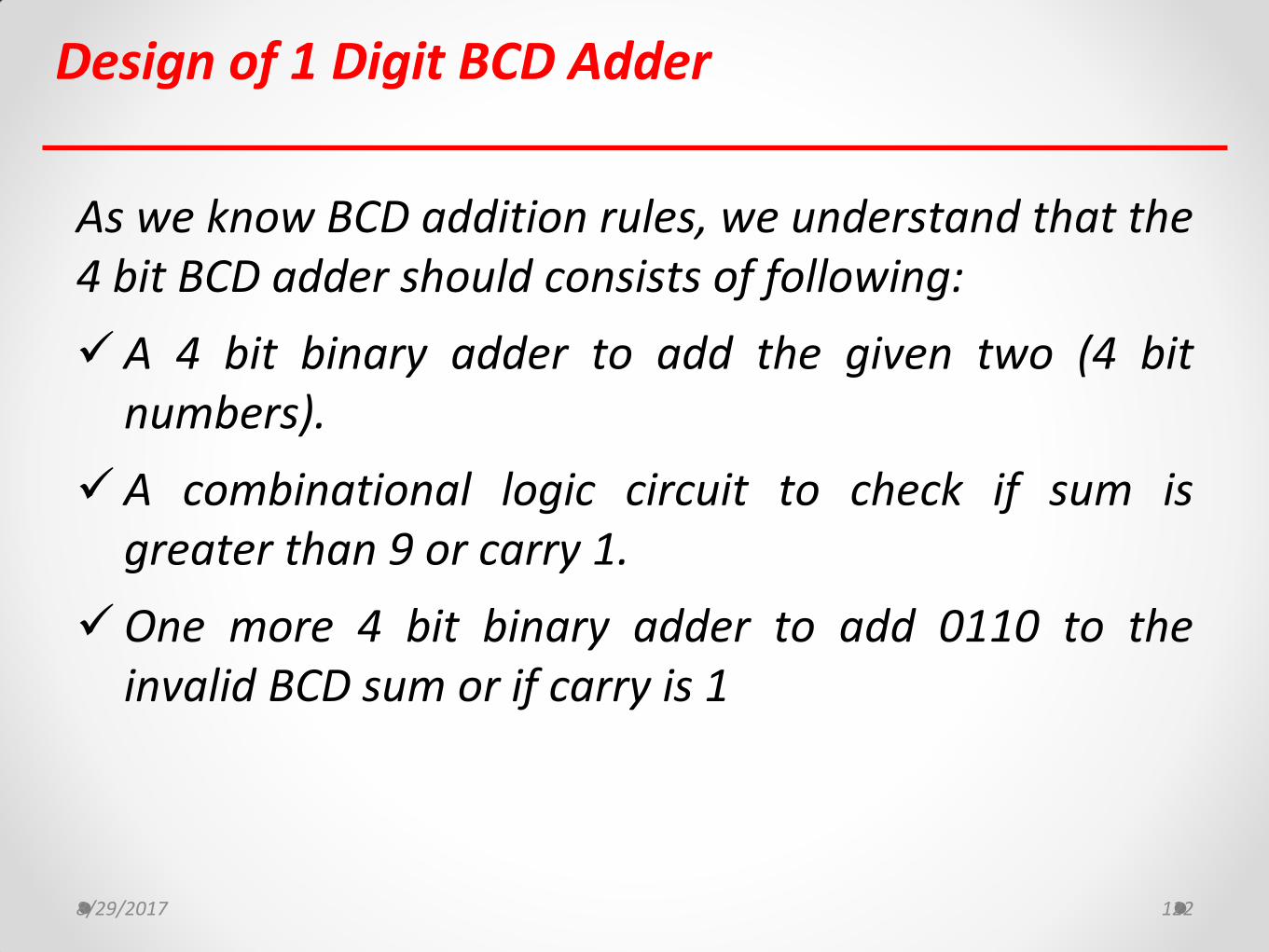
As we know BCD addition rules, we understand that the 4 bit BCD adder should consists of following:
A 4 bit binary adder to add the given two (4 bit numbers).
A combinational logic circuit to check if sum is greater than 9 or carry 1.
One more 4 bit binary adder to add 0110 to the invalid BCD sum or if carry is 1
8/29/2017 122
Design of 1 Digit BCD Adder
8/29/2017 Amit Nevase 123
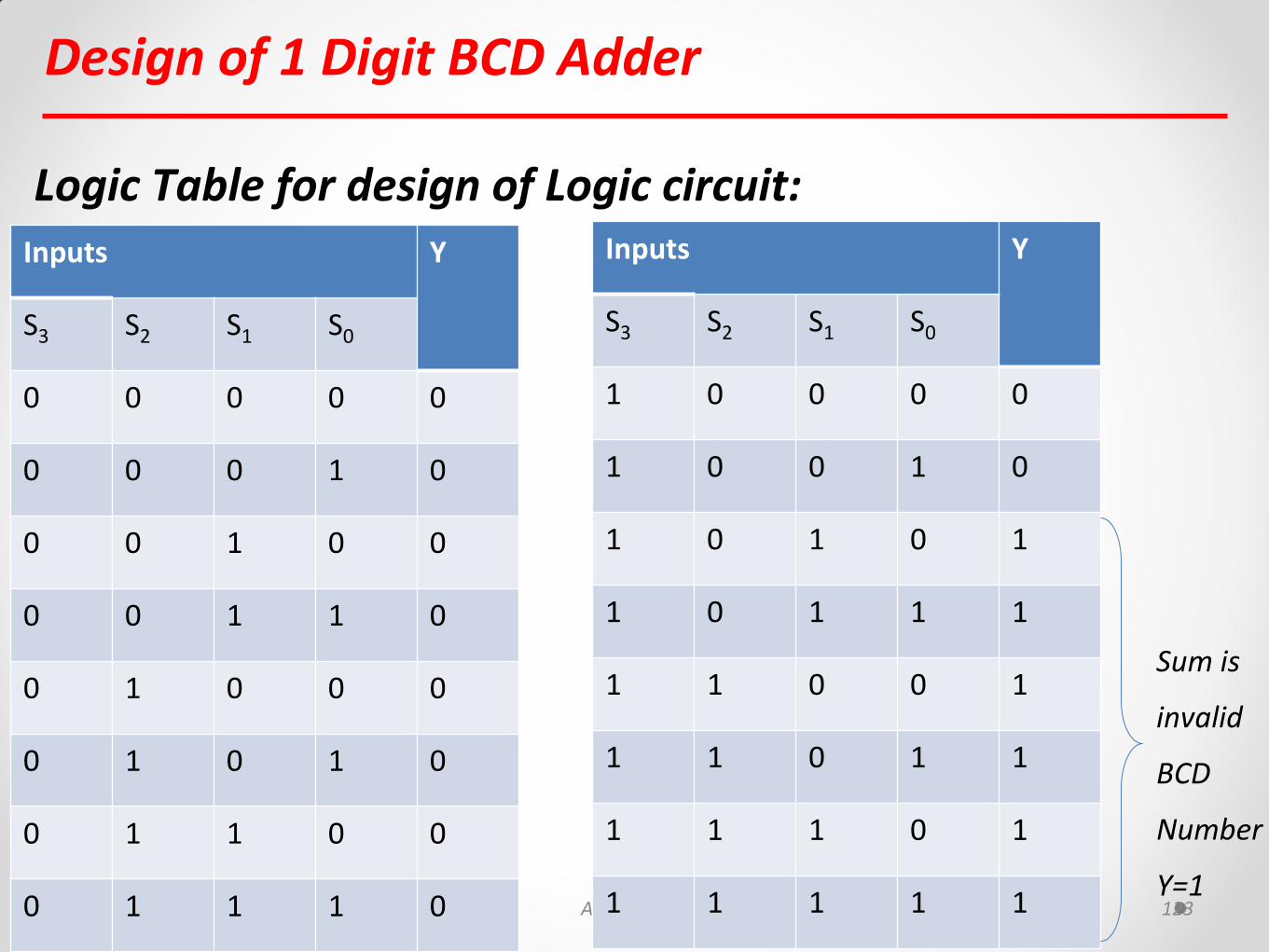
Logic Table for design of Logic circuit: Inputs Y
S3 S2 S1 S0
0 0 0 0 0
0 0 0 1 0
0 0 1 0 0
0 0 1 1 0
0 1 0 0 0
0 1 0 1 0
0 1 1 0 0
0 1 1 1 0
Inputs Y
S3 S2 S1 S0
1 0 0 0 0
1 0 0 1 0
1 0 1 0 1
1 0 1 1 1
1 1 0 0 1
1 1 0 1 1
1 1 1 0 1
1 1 1 1 1
Sum is
invalid
BCD
Number
Y=1
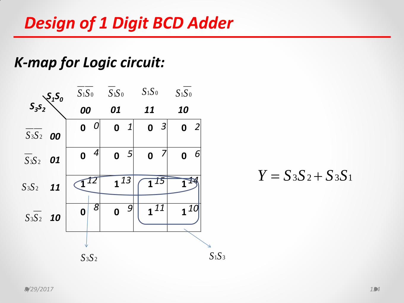
Design of 1 Digit BCD Adder
8/29/2017 124
K-map for Logic circuit:
0 0 0 0
0 0 0 0
1 1 1 1
0 0 1 1
S3s2 00 01 11 10
00
01
11
10
0 1 3 2
4 5 7 6
8 9 11 10
12 13 15 14
S1S0
3 2S S
3 2S S
3 2S S
3 2S S
1 0S S 1 0S S 1 0S S 1 0S S
3 2S S
3 2 3 1Y S S S S
1 3S S
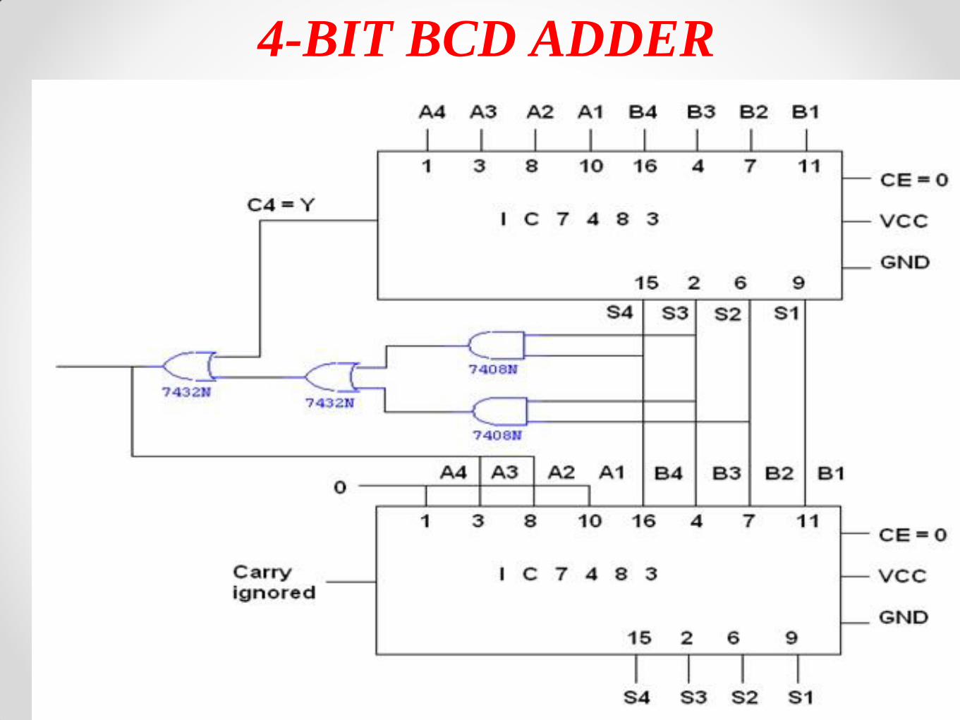
4-BIT BCD ADDER
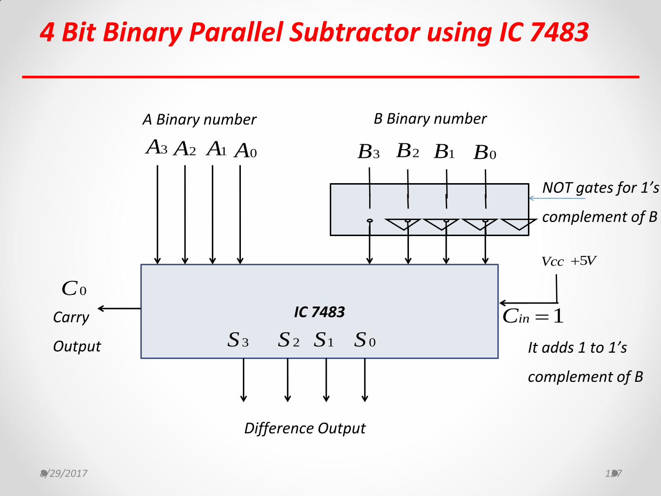
4 Bit Binary Parallel Subtractor using IC 7483
8/29/2017 127
Difference Output
IC 7483 Carry
Output It adds 1 to 1’s
complement of B
A Binary number B Binary number
NOT gates for 1’s
complement of B
0A1A2A3A 0B1B2B3B
0S1S2S3S
0C
1inC
Vcc 5V
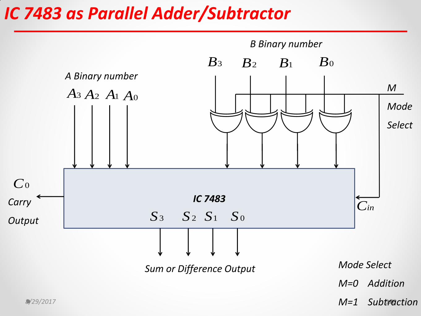
IC 7483 as Parallel Adder/Subtractor
8/29/2017 128
Sum or Difference Output
IC 7483 Carry
Output
Mode Select
M=0 Addition
M=1 Subtraction
A Binary number
B Binary number
M
Mode
Select
0A1A2A3A
0B1B2B3B
0S1S2S3S
0C
inC
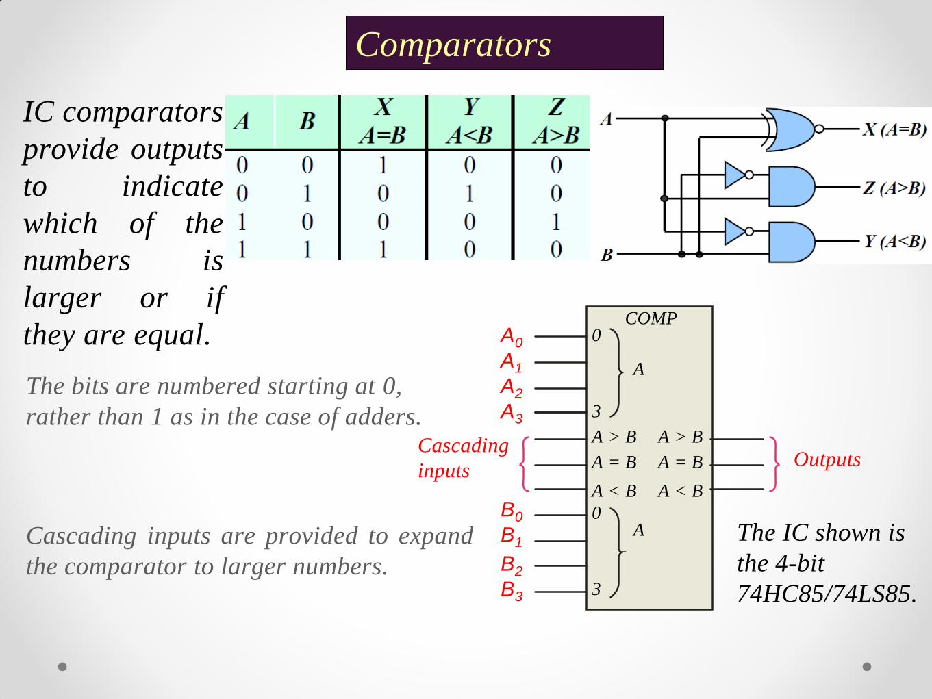
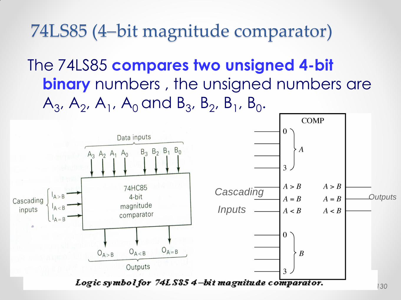
Comparators
IC comparators
provide outputs
to indicate
which of the
numbers is
larger or if
they are equal.
Outputs
A1
A0
A2
A3
B1
B0
B2
B3
Cascading
inputs
COMP
A = B
A < B
A > B
A = B
A < B
A > B
0
0
3
3
A
A The IC shown is
the 4-bit
74HC85/74LS85.
Cascading inputs are provided to expand
the comparator to larger numbers.
The bits are numbered starting at 0,
rather than 1 as in the case of adders.
130
74LS85 (4bit magnitude comparator)
The 74LS85 compares two unsigned 4-bit
binary numbers , the unsigned numbers are
A3, A2, A1, A0 and B3, B2, B1, B0.
Cascading
Inputs
Outputs
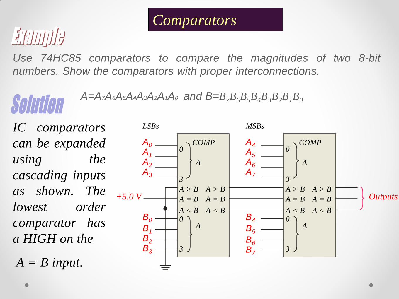
Comparators
IC comparators
can be expanded
using the
cascading inputs
as shown. The
lowest order
comparator has
a HIGH on the
A = B input.
Outputs
A1 A0
A2 A3
B1
B0
B2 B3
COMP
A = B
A < B
A > B
A = B
A < B
A > B
0
0
3
3
A
A
A5 A4
A6 A7
B5
B4
B6 B7
+5.0 V
COMP
A = B
A < B
A > B
A = B
A < B
A > B
0
0
3
3
A
A
LSBs MSBs
Use 74HC85 comparators to compare the magnitudes of two 8-bit
numbers. Show the comparators with proper interconnections.
A=A7A6A5A4A3A2A1A0 and B=B7B6B5B4B3B2B1B0
Combinational Logic Circuits
Introduction
Standard representation of canonical forms (SOP & POS), Maxterm and Minterm , Conversion between SOP and POS forms
K-map reduction techniques upto 4 variables (SOP & POS form), Design of Half Adder, Full Adder, Half Subtractor & Full Subtractor using k-Map
Code Converter using K-map: Gray to Binary, Binary to Gray Code Converter (upto 4 bit)
IC 7447 as BCD to 7- Segment decoder driver
IC 7483 as Adder & Subtractor, 1 Digit BCD Adder
Block Schematic of ALU IC 74181, IC 74381
8/29/2017 132
IC 74181 – Arithmetic Logic Unit
A very popular & widely used combinational circuit is ALU which is capable of performing arithmetic as well as logical operation.
Arithmetic Operating Modes:
Addition
Subtraction
Shift Operation
Magnitude Comparison
12 other arithmetic operations 8/29/2017 133
IC 74181
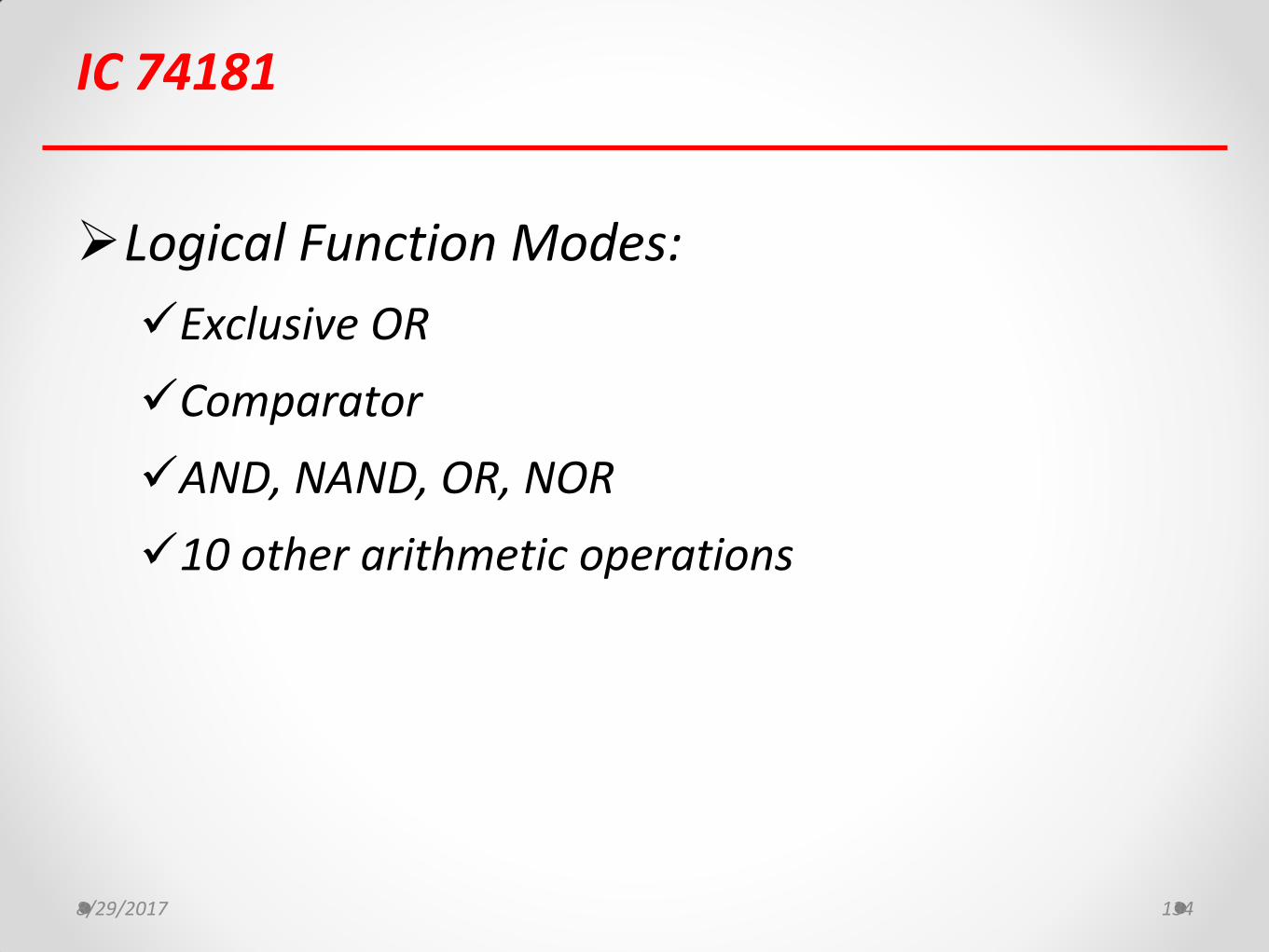
Logical Function Modes:
Exclusive OR
Comparator
AND, NAND, OR, NOR
10 other arithmetic operations
8/29/2017 134
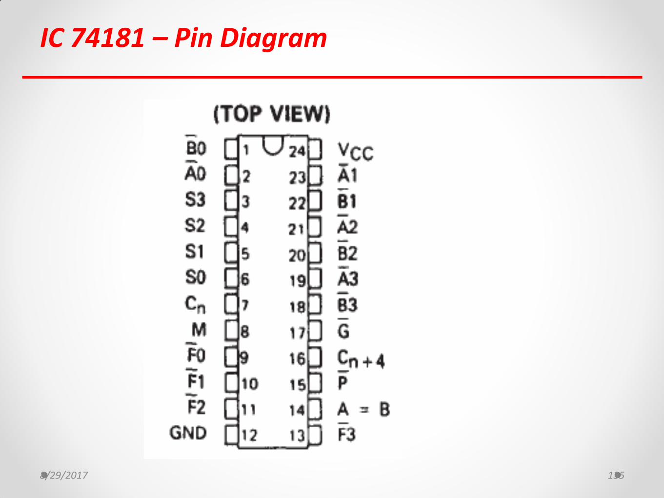
IC 74181 – Pin Diagram
8/29/2017 135
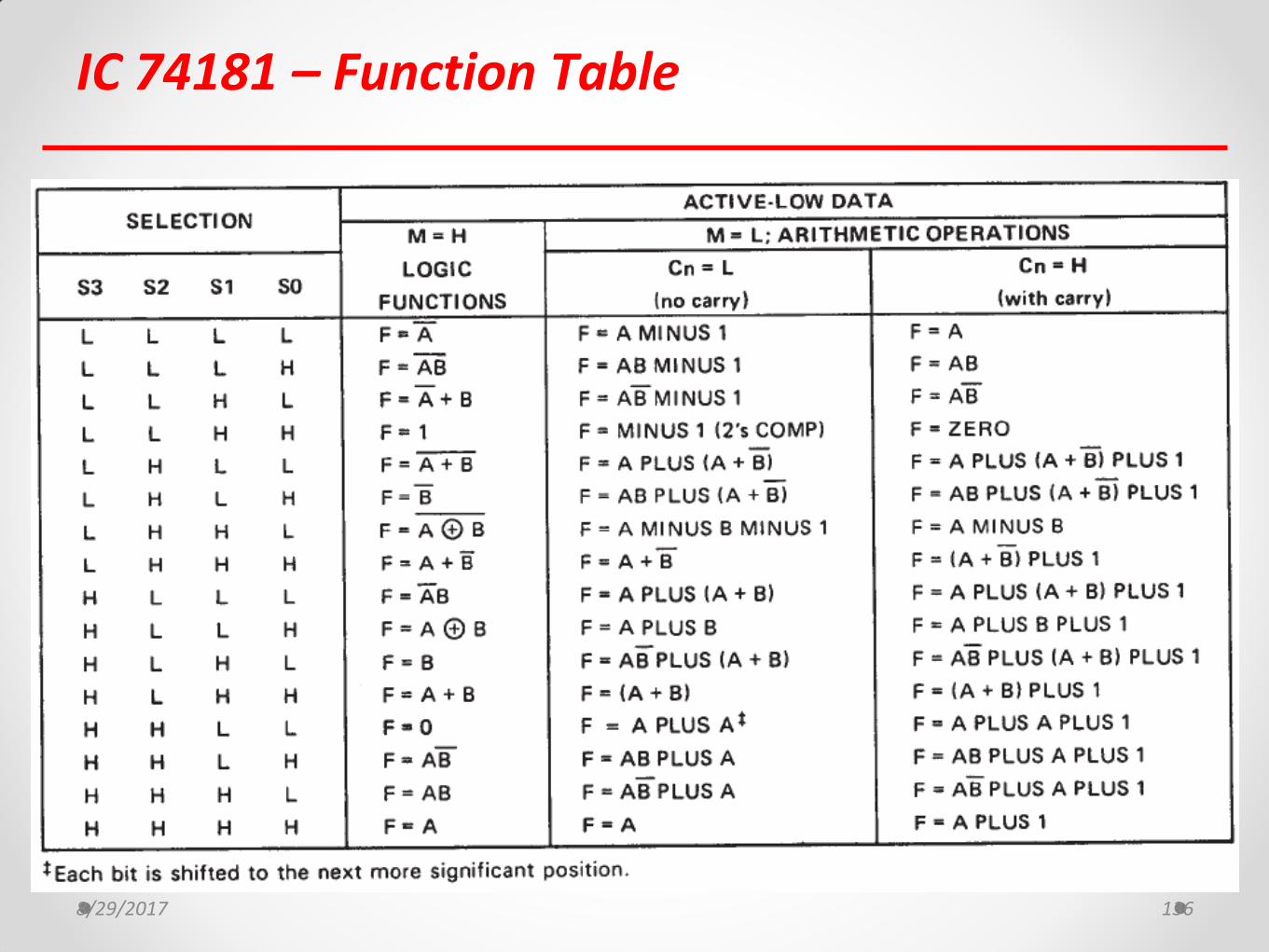
IC 74181 – Function Table
8/29/2017 136
IC 74381 – 4 Bit Arithmetic Logic Unit
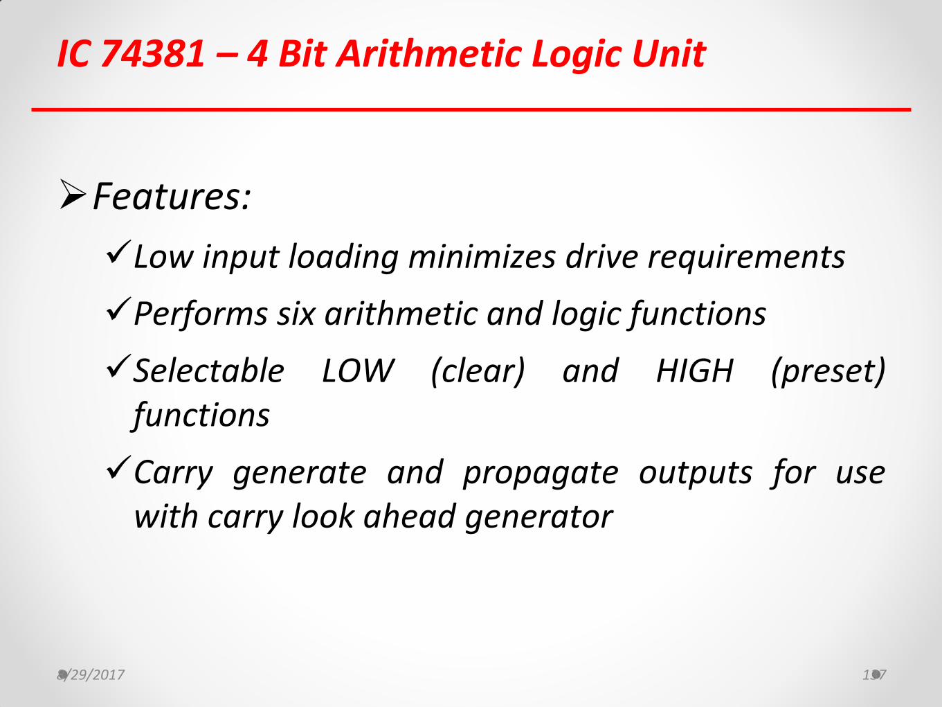
Features:
Low input loading minimizes drive requirements
Performs six arithmetic and logic functions
Selectable LOW (clear) and HIGH (preset) functions
Carry generate and propagate outputs for use with carry look ahead generator
8/29/2017 137
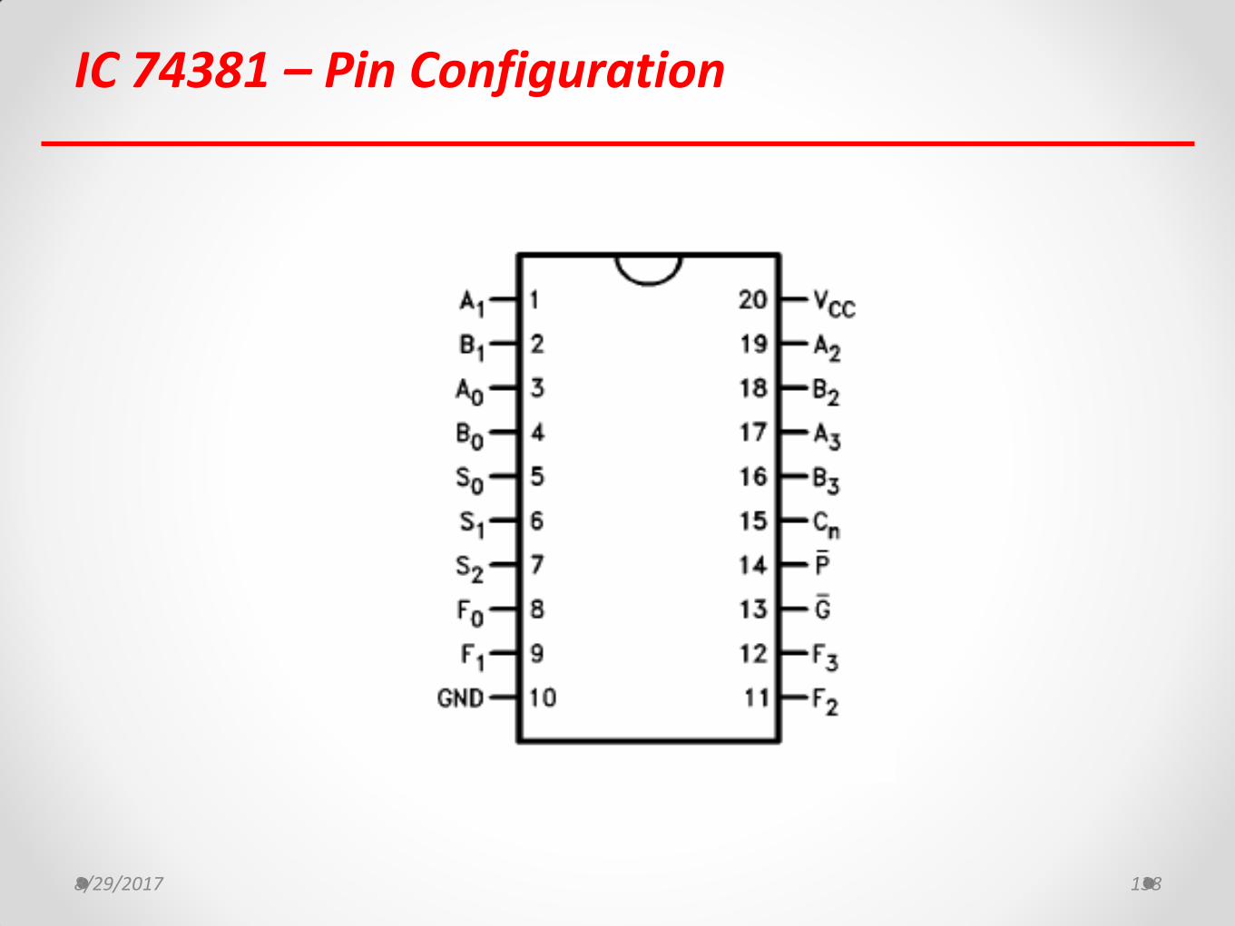
IC 74381 – Pin Configuration
8/29/2017 138
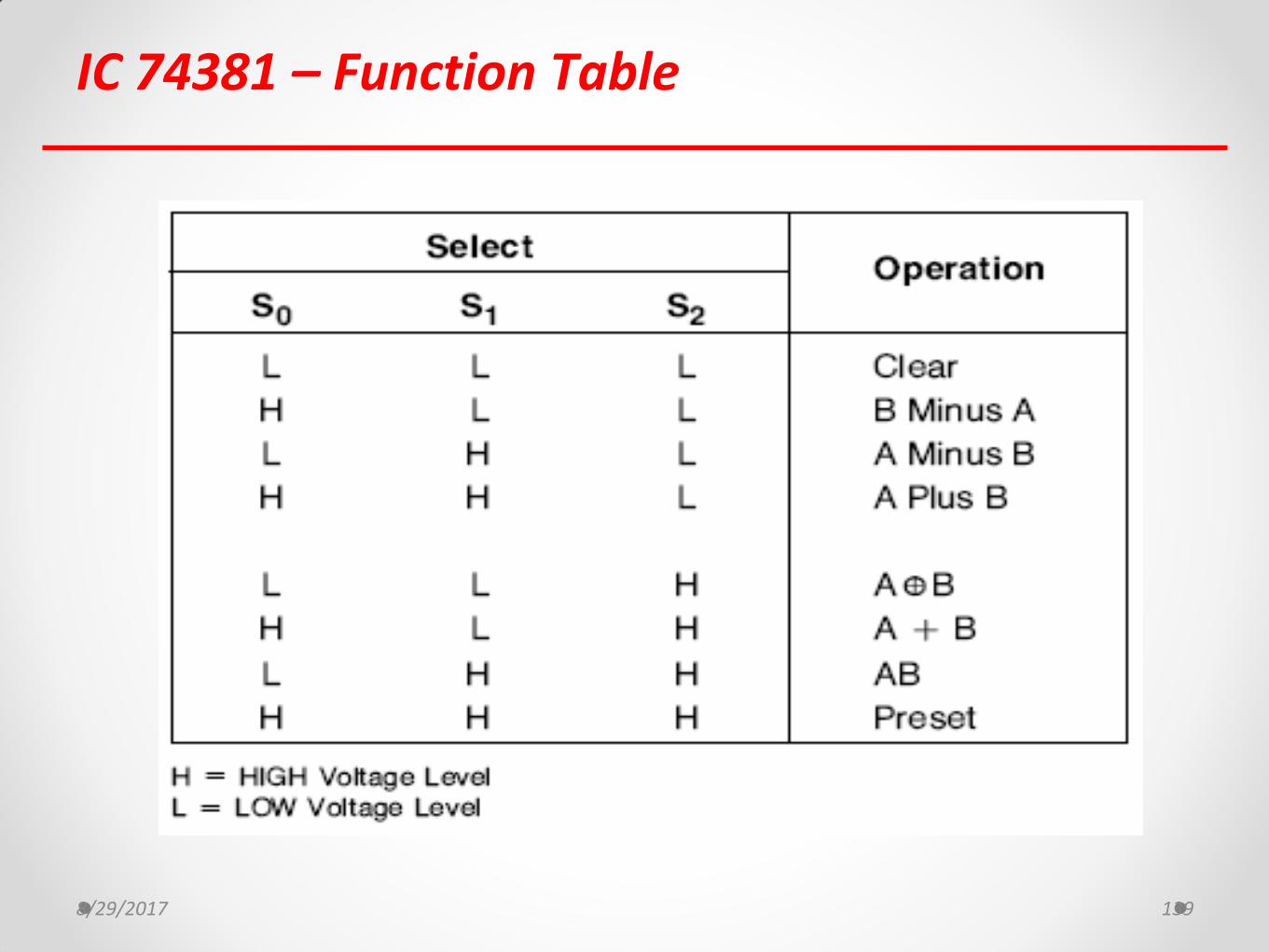
IC 74381 – Function Table
8/29/2017 139
Combinational Logic Circuits
Necessity, Applications and Realization of following
Multiplexers (MUX): MUX Tree
Demultiplexers (DEMUX): DEMUX Tree, DEMUX as Decoder
Study of IC 74151, IC 74155
Priority Encoder 8:3, Decimal to BCD Encoder
Tristate Logic, Unidirectional & Bidirectional buffer ICs: IC 74244 and IC 74245
8/29/2017 140

Multiplexers
Multiplexer is a circuit which has a number of inputs but only one output.
Multiplexer is a circuit which transmits large number of information signals over a single line.
Multiplexer is also known as “Data Selector” or MUX.
8/29/2017 141

Necessity of Multiplexers
In most of the electronic systems, the digital data is available on more than one lines. It is necessary to route this data over a single line.
Under such circumstances we require a circuit which select one of the many inputs at a time.
This circuit is nothing but a multiplexer. Which has many inputs, one output and some select lines.
Multiplexer improves the reliability of the digital system because it reduces the number of external wired connections.
8/29/2017 142
Advantages of Multiplexers
It reduces the number of wires.
So it reduces the circuit complexity and cost.
We can implement many combinational circuits using Mux.
It simplifies the logic design.
It does not need the k-map and simplification.
8/29/2017 143
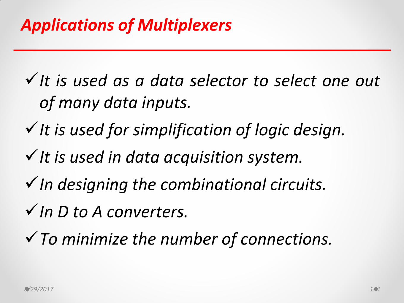
Applications of Multiplexers
It is used as a data selector to select one out of many data inputs.
It is used for simplification of logic design.
It is used in data acquisition system.
In designing the combinational circuits.
In D to A converters.
To minimize the number of connections.
8/29/2017 144
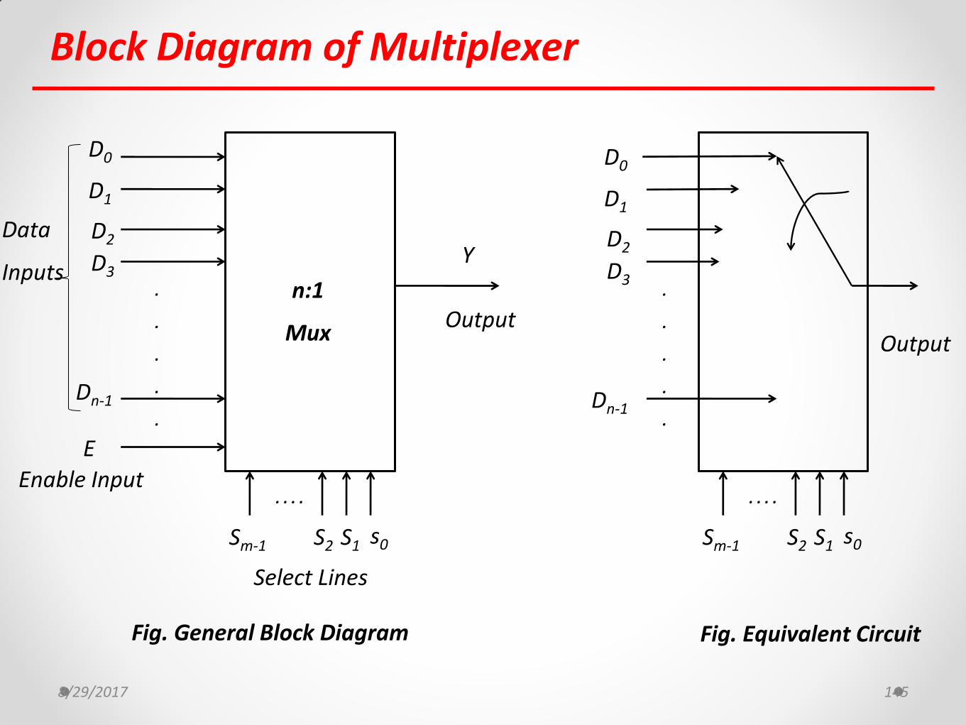
Block Diagram of Multiplexer
8/29/2017 145
Data
Inputs
Select Lines
Output n:1
Mux
E
Enable Input
Y
D0
D1
D2
D3
Dn-1
s0 S1 S2 Sm-1
.
.
.
.
.
. . . .
Output
D0
D1
D2
D3
Dn-1
s0 S1 S2 Sm-1
.
.
.
.
.
. . . .
Fig. General Block Diagram Fig. Equivalent Circuit
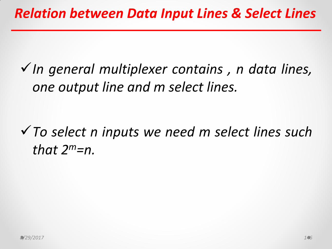
Relation between Data Input Lines & Select Lines
In general multiplexer contains , n data lines, one output line and m select lines.
To select n inputs we need m select lines such that 2m=n.
8/29/2017 146
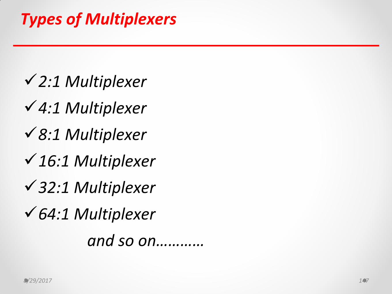
Types of Multiplexers
2:1 Multiplexer
4:1 Multiplexer
8:1 Multiplexer
16:1 Multiplexer
32:1 Multiplexer
64:1 Multiplexer
and so on…………
8/29/2017 147
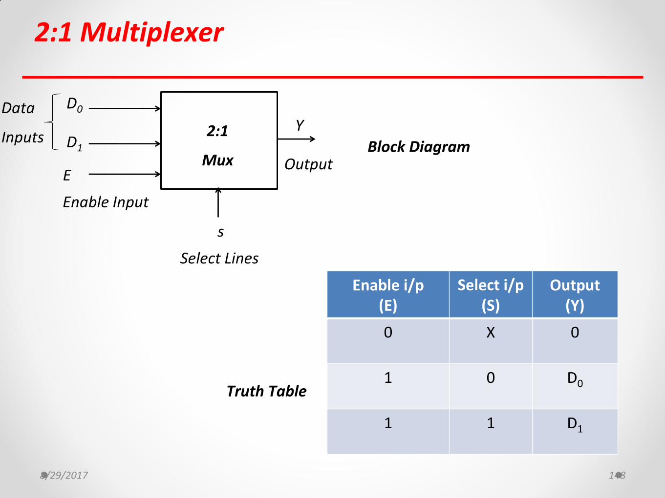
2:1 Multiplexer
8/29/2017 148
Select Lines
Output
2:1
Mux E
Enable Input
Y
D0
D1
s
Data
Inputs
Enable i/p (E)
Select i/p (S)
Output (Y)
0 X 0
1 0 D0
1 1 D1
Block Diagram
Truth Table

Realization of 2:1 Mux using gates
8/29/2017 149
S D1 D0
Output
E
Enable Input
Y
0SD
1SD
S
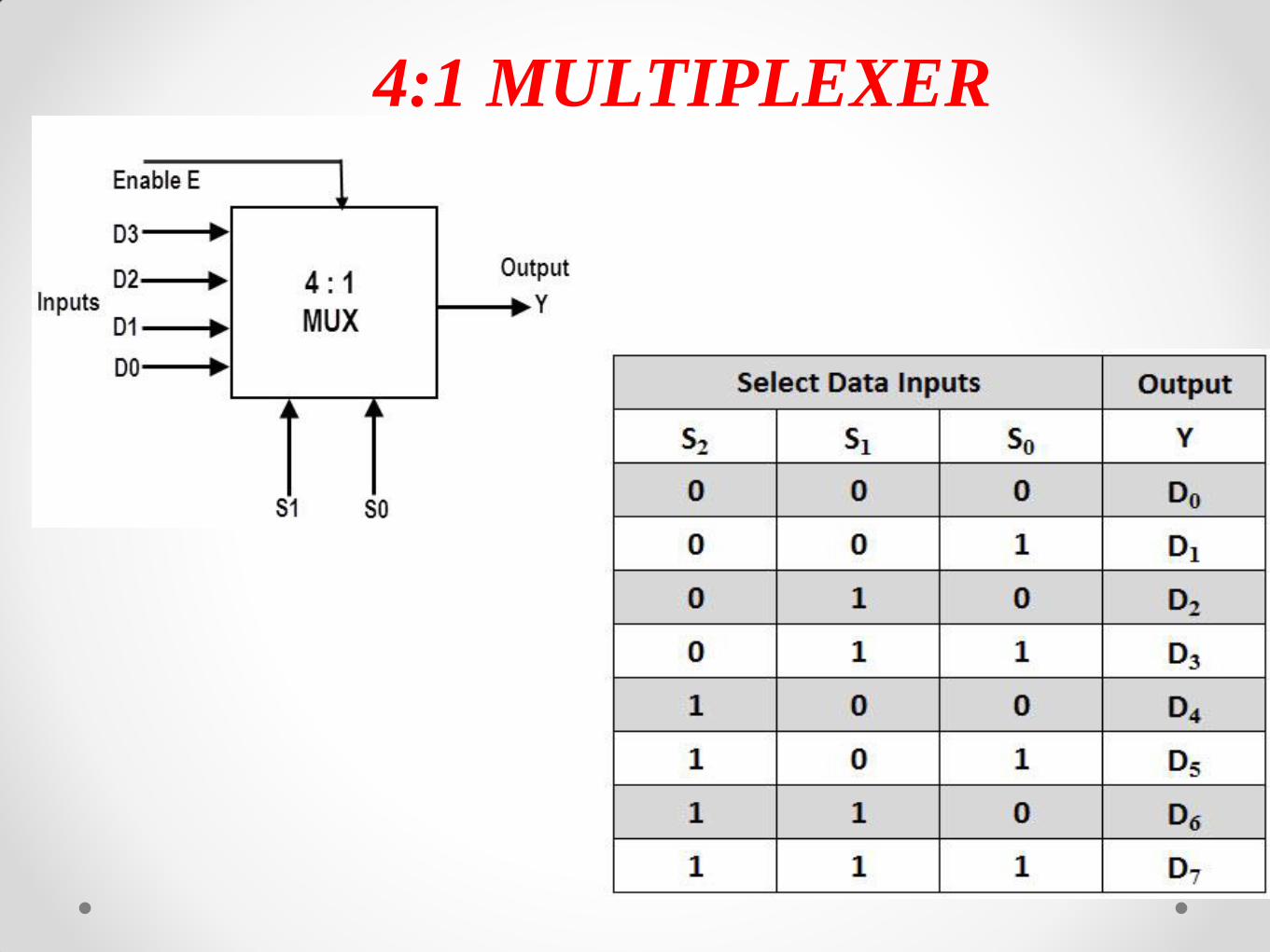
4:1 MULTIPLEXER
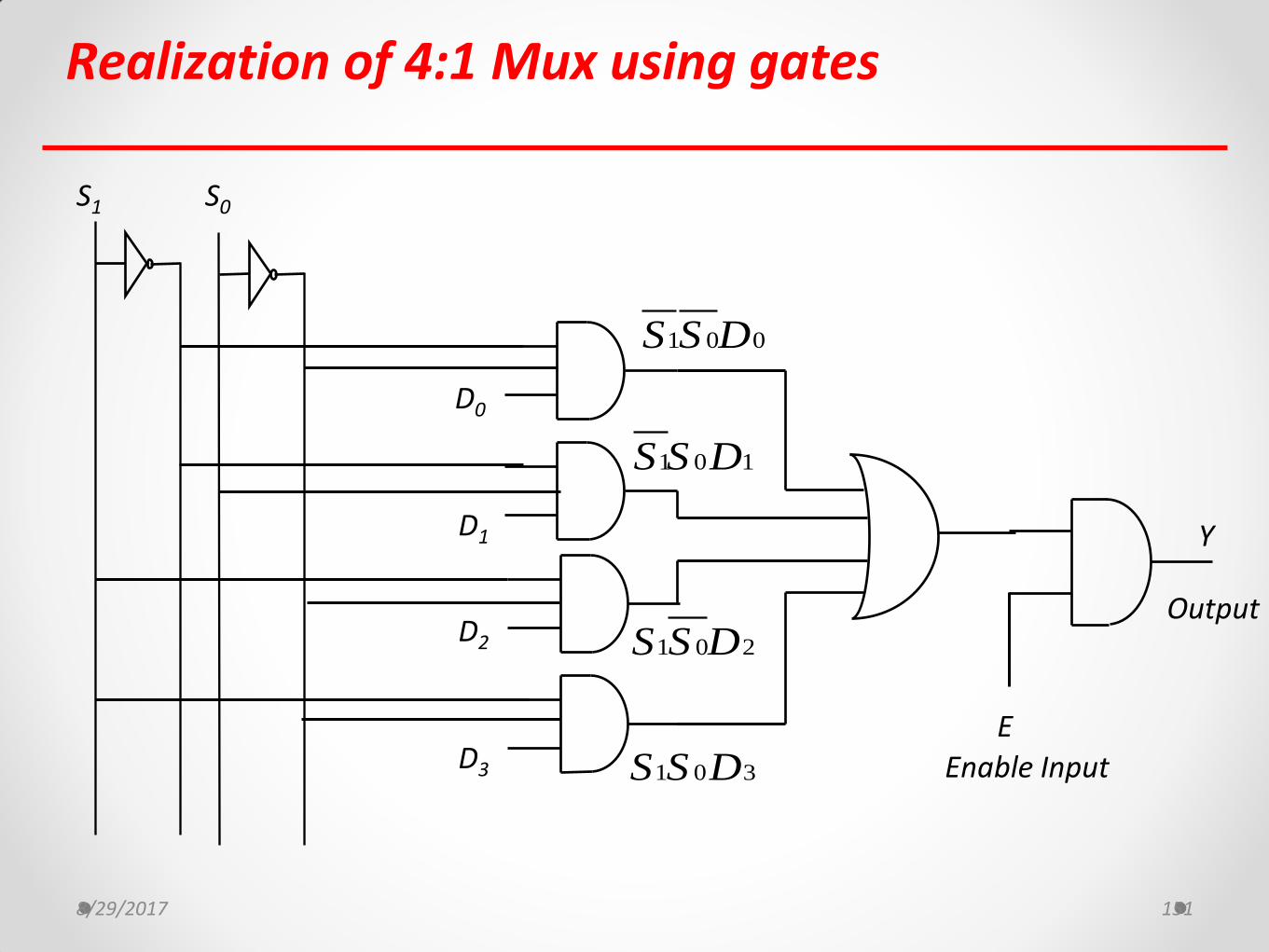
Realization of 4:1 Mux using gates
8/29/2017 151
Output
E
Enable Input
Y
S1 S0
D0
D1
D2
D3
1 0 0S S D
1 0 1S S D
1 0 2S S D
1 0 3S S D
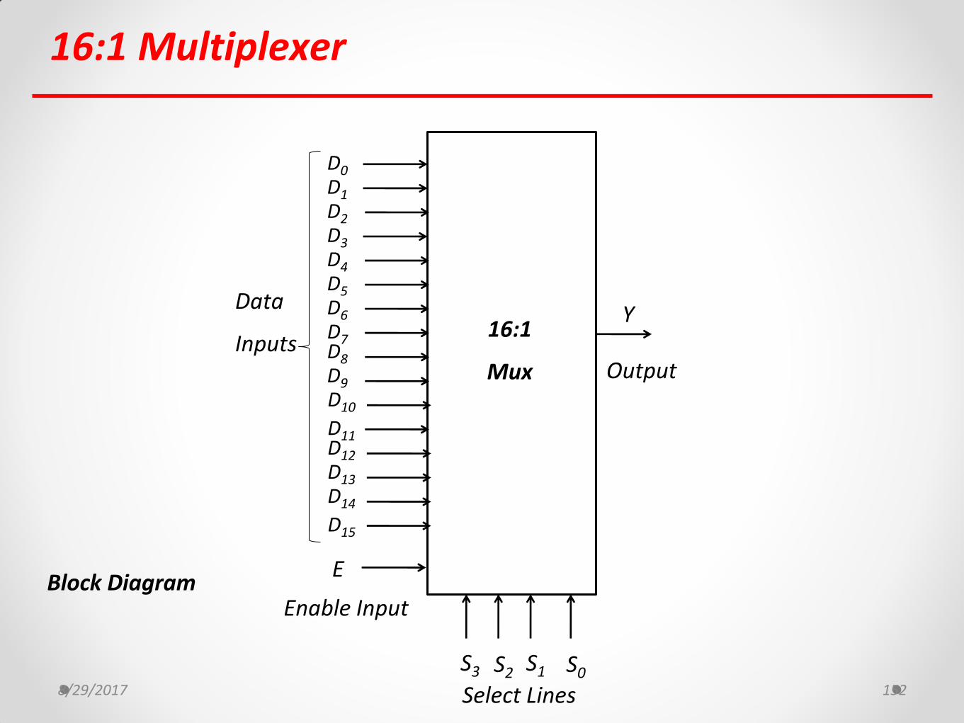
16:1 Multiplexer
8/29/2017 152 Select Lines
Output
16:1
Mux
E
Enable Input
Y
D0 D1
Data
Inputs
Block Diagram
D2 D3
S0 S2
D4 D5 D6 D7
S1
D8 D9 D10
D11 D12 D13 D14
D15
S3
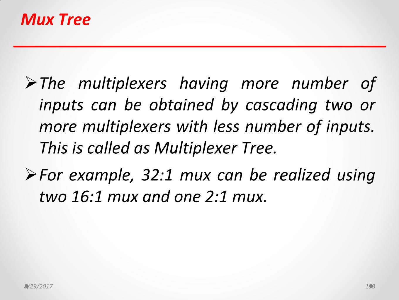
Mux Tree
The multiplexers having more number of inputs can be obtained by cascading two or more multiplexers with less number of inputs. This is called as Multiplexer Tree.
For example, 32:1 mux can be realized using two 16:1 mux and one 2:1 mux.
8/29/2017 153
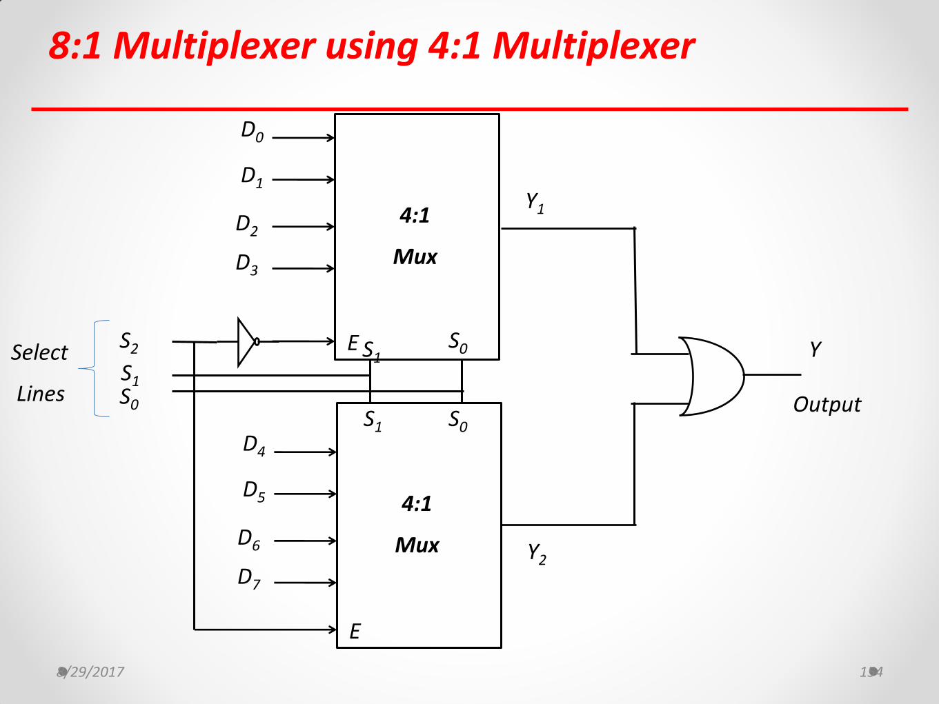
8:1 Multiplexer using 4:1 Multiplexer
8/29/2017 154
Select
Lines
4:1
Mux
E
Y1
D0
D1
D2
D3
S0
S1
Output
4:1
Mux
E
D4
D5
D6
D7
S0
S1
S1
S0
S2
Y2
Y
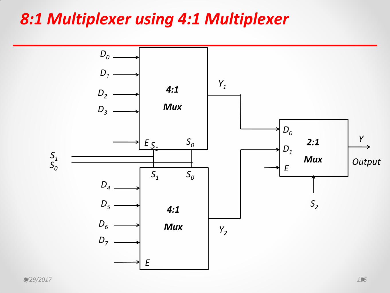
8:1 Multiplexer using 4:1 Multiplexer
8/29/2017 155
4:1
Mux
E
Y1
D0
D1
D2
D3
S0
S1
4:1
Mux
E
D4
D5
D6
D7
S0
S1
S1
S0
S2
Y2
Output
2:1
Mux E
Y D0
D1
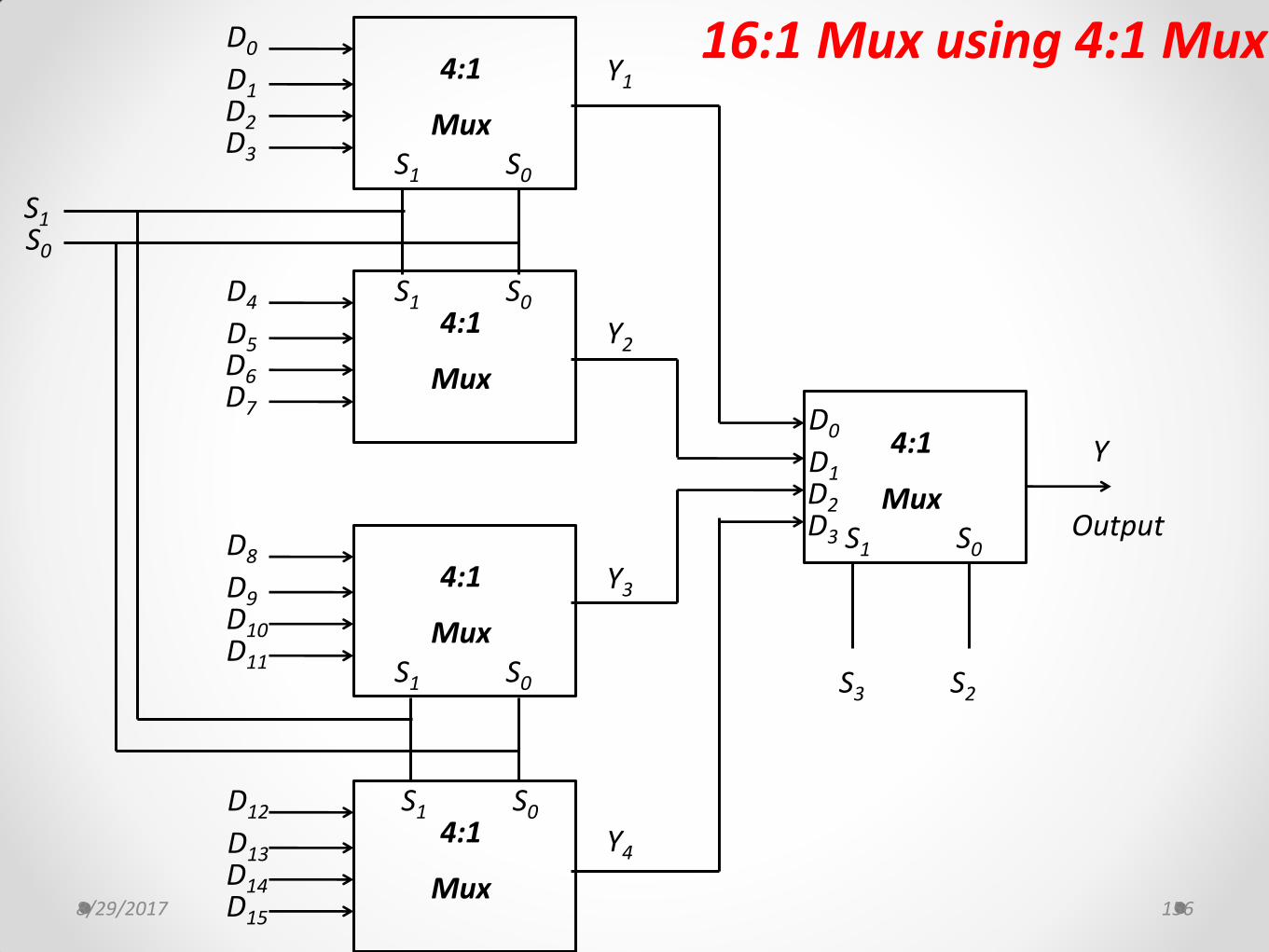
16:1 Mux using 4:1 Mux
8/29/2017 156
4:1
Mux
D0
D1 D2 D3
S0 S1
4:1
Mux
D4
D5 D6 D7
4:1
Mux
D8
D9 D10 D11
4:1
Mux
D12
D13 D14 D15
S0 S1
S0 S1
S0 S1
S1 S0
4:1
Mux
S0 S1
S2 S3
Output
Y
Y1
Y2
Y3
Y4
D0
D1 D2 D3
Realization of Boolean expression using Mux
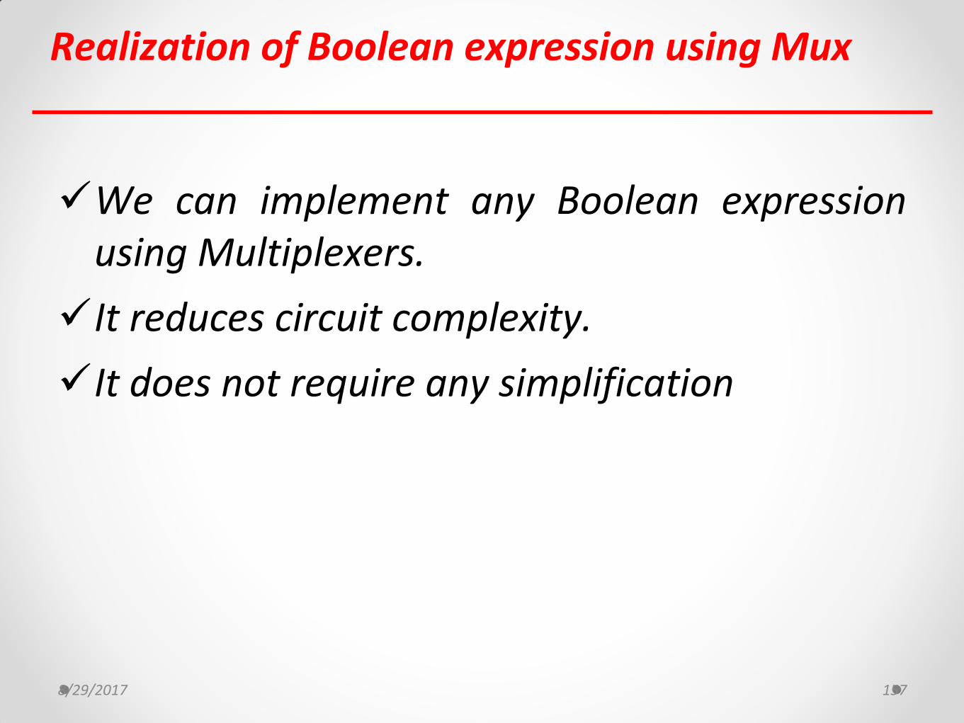
We can implement any Boolean expression using Multiplexers.
It reduces circuit complexity.
It does not require any simplification
8/29/2017 157

Example 1
8/29/2017 158
Implement following Boolean expression using multiplexer
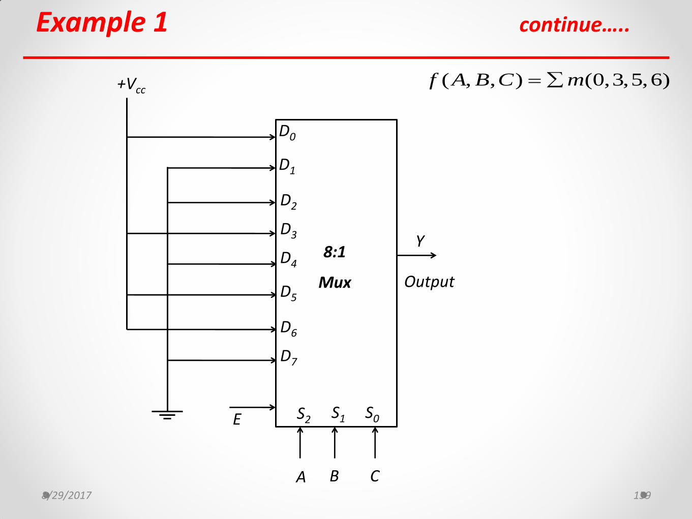
Since there are three variables, therefore a multiplexer with three select input is required i.e. 8:1 multiplexer is required
The 8:1 multiplexer is configured as below to implement given Boolean expression
( , , ) (0,3,5,6)f A B C m
Example 1 continue…..
8/29/2017 159
Output
8:1
Mux
E
Y
D0
D1
D2
D3
S0 S2
D4
D5
D6
D7
S1
A B C
+Vcc ( , , ) (0,3,5,6)f A B C m
Example 2
8/29/2017 160
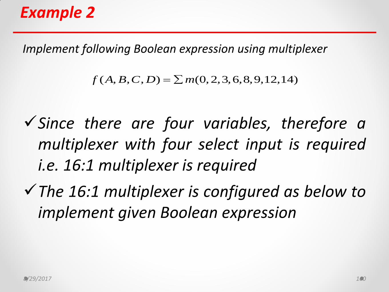
Implement following Boolean expression using multiplexer
Since there are four variables, therefore a multiplexer with four select input is required i.e. 16:1 multiplexer is required
The 16:1 multiplexer is configured as below to implement given Boolean expression
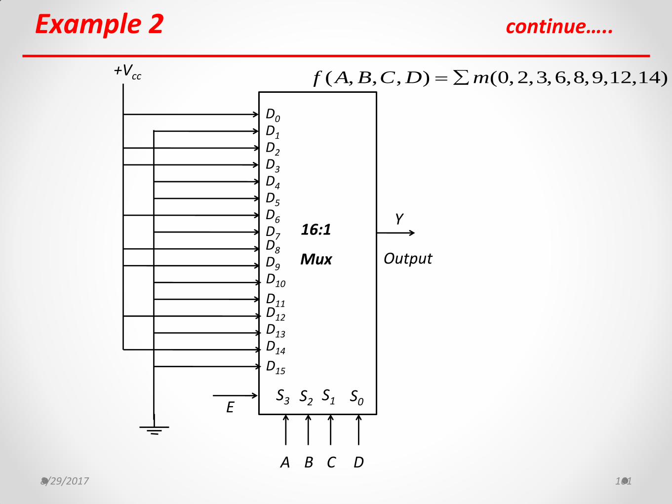
( , , , ) (0,2,3,6,8,9,12,14)f A B C D m
Example 2 continue…..
8/29/2017 161
Output
16:1
Mux
E
Y
D0 D1 D2 D3
S0 S2
D4 D5 D6 D7
S1
D8 D9 D10
D11 D12 D13 D14
D15
S3
A B C
+Vcc
D
( , , , ) (0,2,3,6,8,9,12,14)f A B C D m

Combinational Logic Circuits
Necessity, Applications and Realization of following
Multiplexers (MUX): MUX Tree
Demultiplexers (DEMUX): DEMUX Tree, DEMUX as Decoder
Study of IC 74151, IC 74155
Priority Encoder 8:3, Decimal to BCD Encoder
Tristate Logic, Unidirectional & Bidirectional buffer ICs: IC 74244 and IC 74245
8/29/2017 162
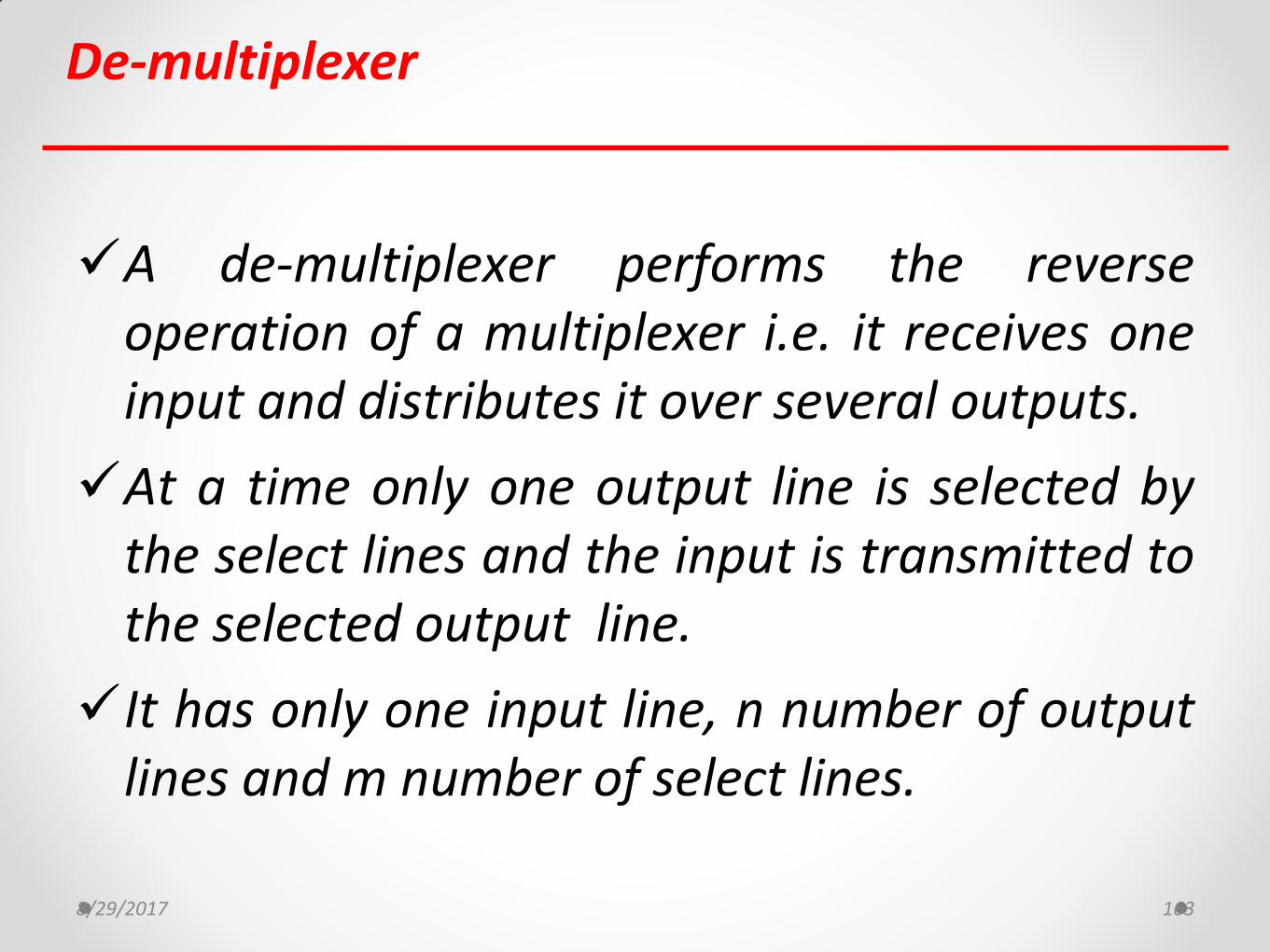
De-multiplexer
A de-multiplexer performs the reverse operation of a multiplexer i.e. it receives one input and distributes it over several outputs.
At a time only one output line is selected by the select lines and the input is transmitted to the selected output line.
It has only one input line, n number of output lines and m number of select lines.
8/29/2017 163
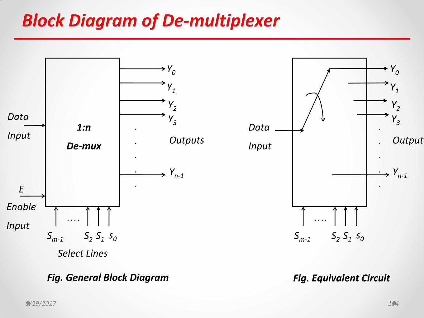
Block Diagram of De-multiplexer
8/29/2017 164
Data
Input
Select Lines
Outputs 1:n
De-mux
E
Enable
Input
Y0
Y1
Y2
Y3
Yn-1
s0 S1 S2 Sm-1
.
.
.
.
.
. . . .
s0 S1 S2 Sm-1
.
.
.
.
.
. . . .
Fig. General Block Diagram Fig. Equivalent Circuit
Data
Input Outputs
Y0
Y1
Y2
Y3
Yn-1
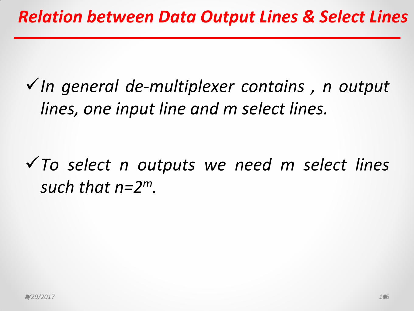
Relation between Data Output Lines & Select Lines
In general de-multiplexer contains , n output lines, one input line and m select lines.
To select n outputs we need m select lines such that n=2m.
8/29/2017 165
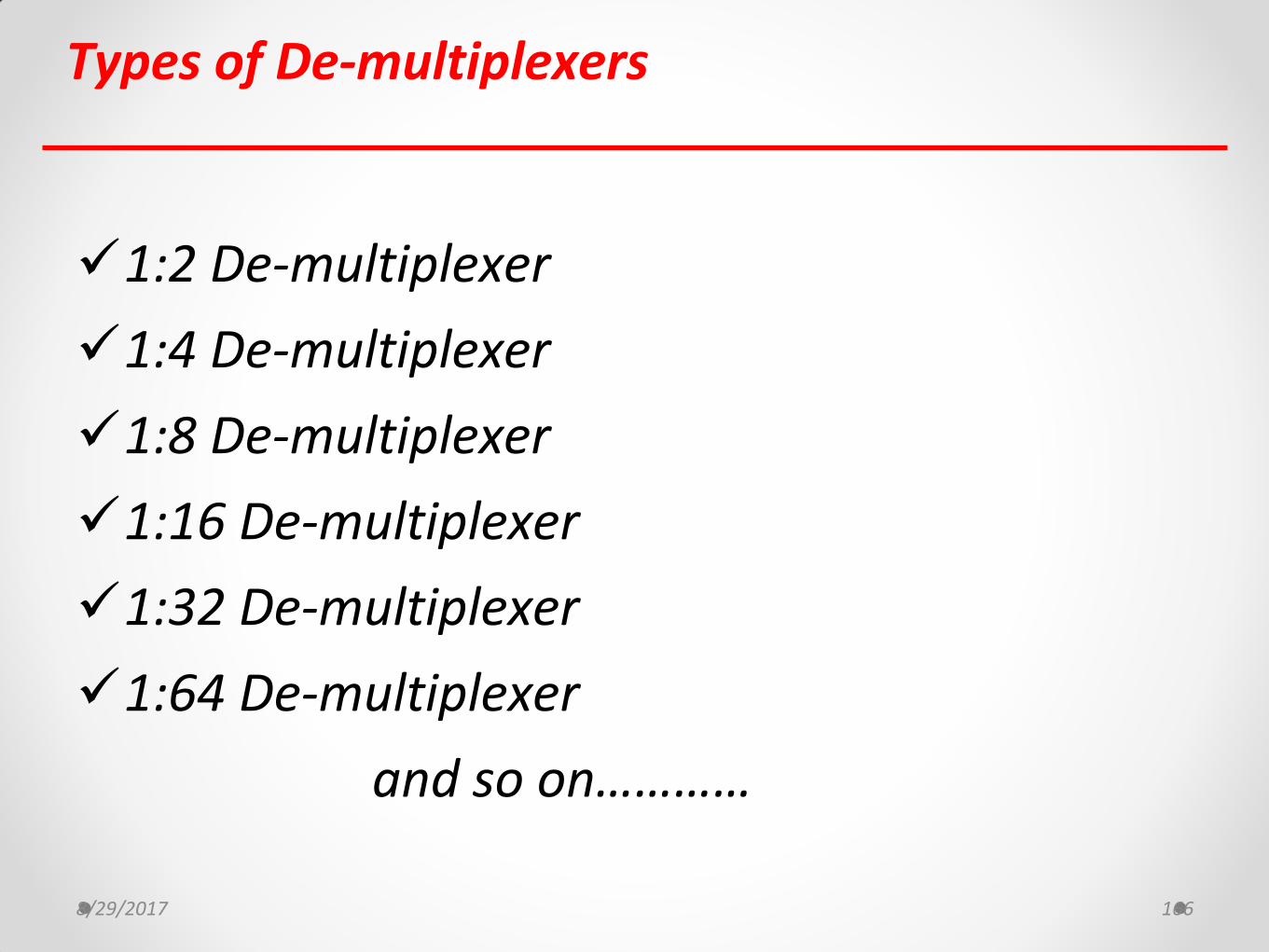
Types of De-multiplexers
1:2 De-multiplexer
1:4 De-multiplexer
1:8 De-multiplexer
1:16 De-multiplexer
1:32 De-multiplexer
1:64 De-multiplexer
and so on…………
8/29/2017 166
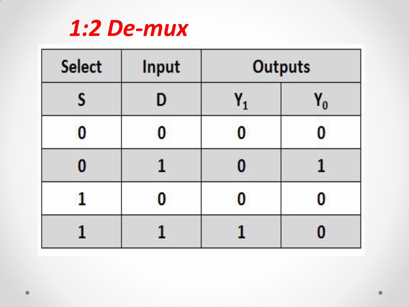
1:2 De-mux
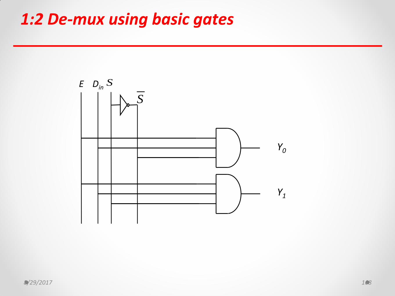
1:2 De-mux using basic gates
8/29/2017 168
E Din
Y0
Y1
S
S

1:4 De-mux
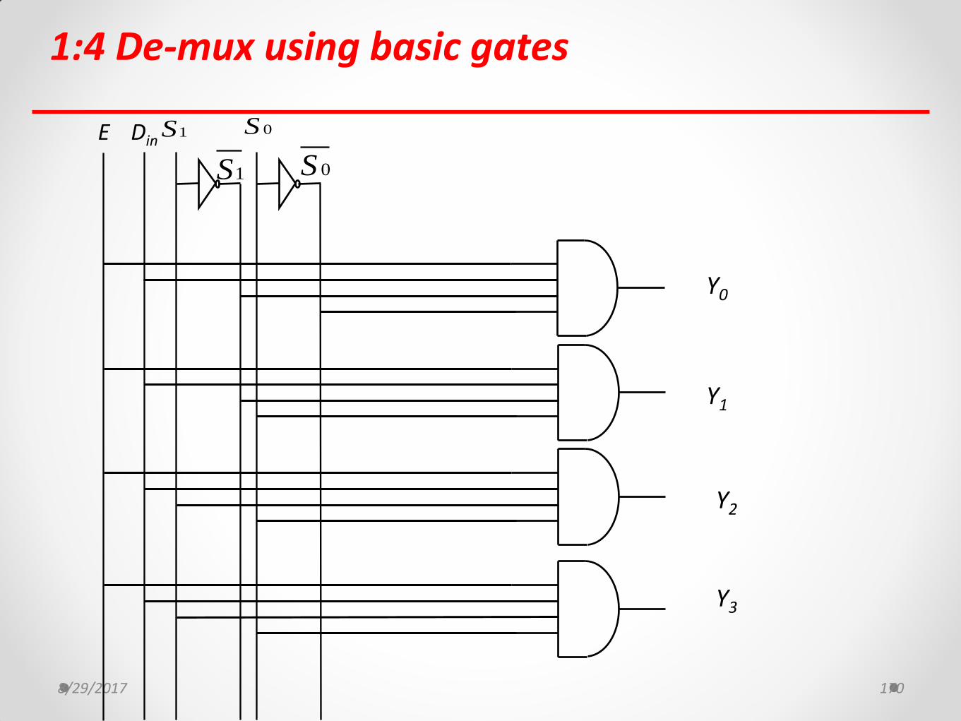
1:4 De-mux using basic gates
8/29/2017 170
E Din
Y0
Y1
Y2
Y3
1S
1S
0S
0S
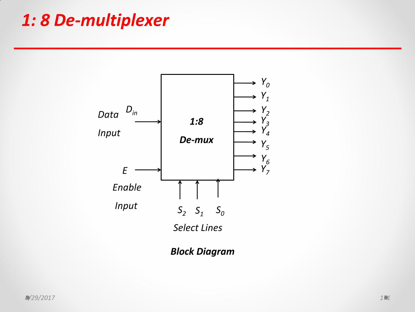
1: 8 De-multiplexer
8/29/2017 171
Select Lines
1:8
De-mux
E
Enable
Input
Y0
Y1
Data
Input
Block Diagram
Din
S0 S1
Y2 Y3 Y4
Y5
Y6 Y7
S2
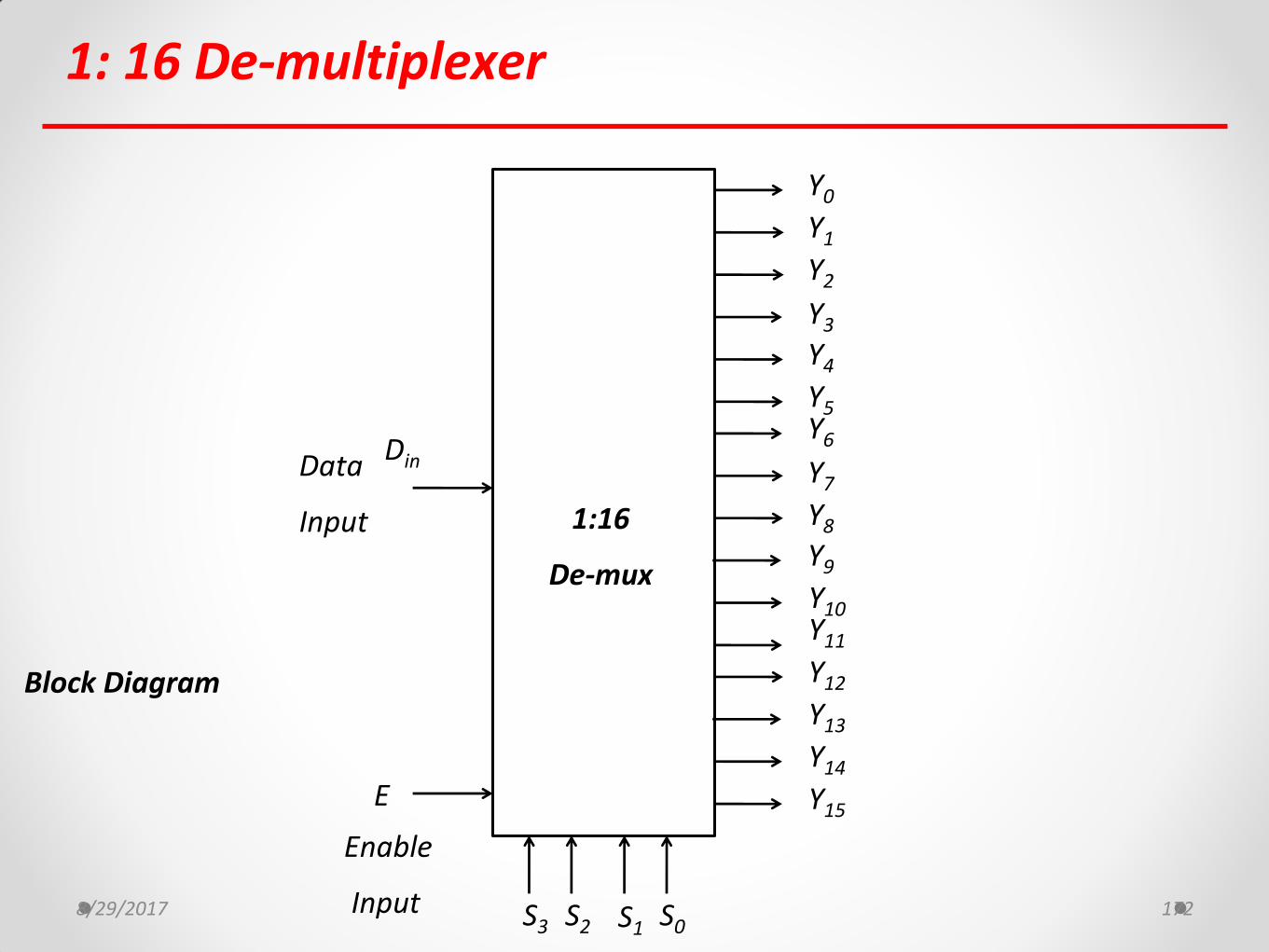
1: 16 De-multiplexer
8/29/2017 172
1:16
De-mux
E
Enable
Input
Y0
Data
Input
Block Diagram
Din
S0 S1 S2
Y1
Y2
Y3
Y4
Y5 Y6
Y7
Y8
Y9
Y10 Y11
Y12
Y13
Y14
Y15
S3
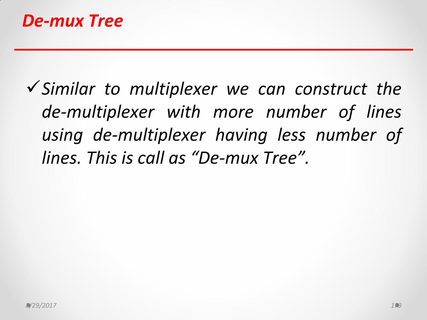
De-mux Tree
Similar to multiplexer we can construct the de-multiplexer with more number of lines using de-multiplexer having less number of lines. This is call as “De-mux Tree”.
8/29/2017 173
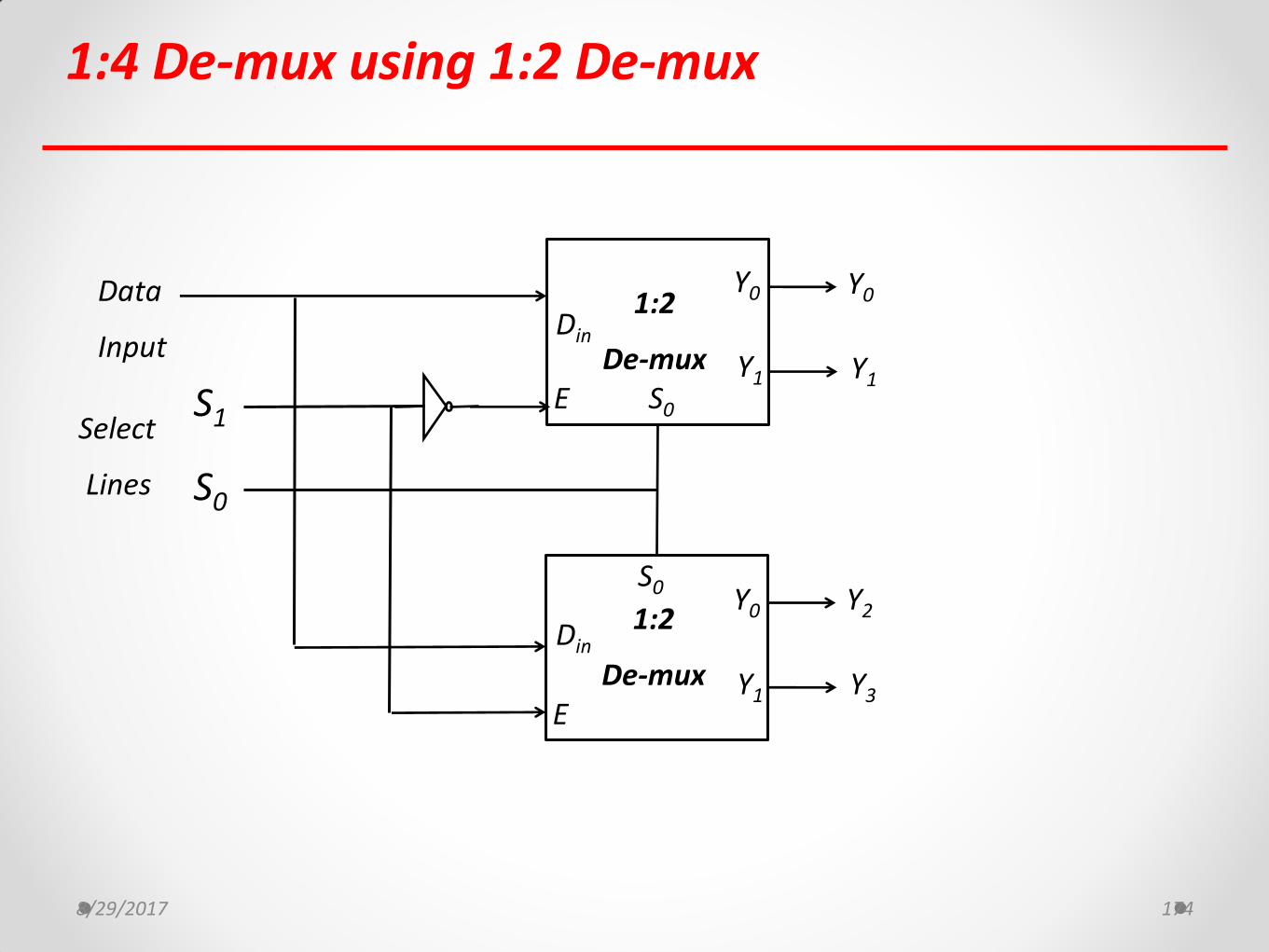
1:4 De-mux using 1:2 De-mux
8/29/2017 174
Select
Lines
1:2
De-mux
E
Y0
Y1
S0
Data
Input Din
1:2
De-mux
E
Y2
Y3
Din
S1
S0
S0
Y0
Y1
Y0
Y1
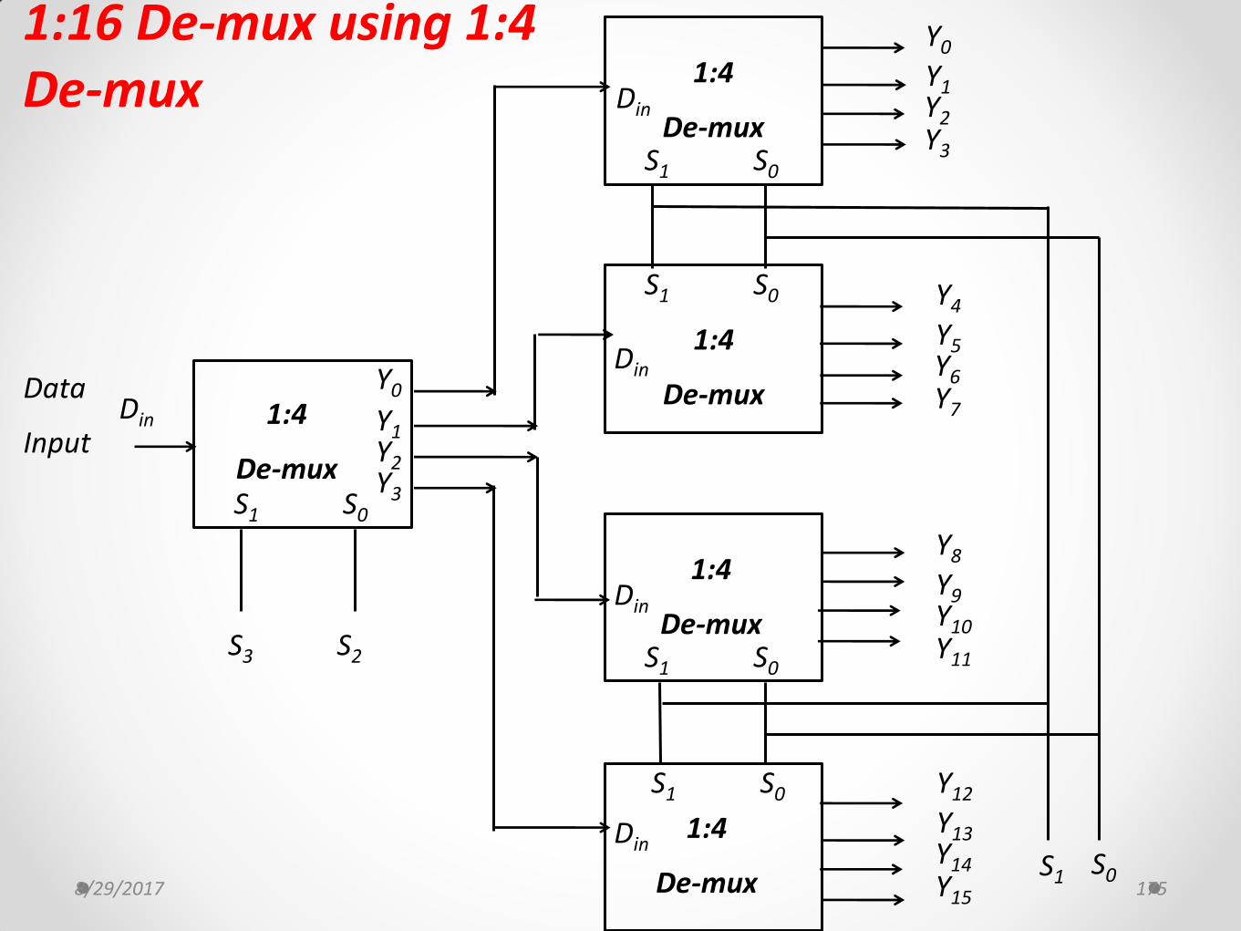
1:16 De-mux using 1:4 De-mux
8/29/2017 175
Y0
Y1 Y2 Y3
S0 S1
S0 S1
S0 S1
S0 S1
1:4
De-mux S0 S1
S2 S3
Data
Input
Y0
S1 S0
Y1 Y2 Y3
Din
Y4
Y5 Y6 Y7
Y8
Y9 Y10 Y11
Y12
Y13 Y14 Y15
Din
Din
Din
Din
1:4
De-mux
1:4
De-mux
1:4
De-mux
1:4
De-mux
Decoder
Decoder is a combinational circuit.
It converts n bit binary information at its input into a maximum of 2n output lines.
For example, if n=2 then we can design upto 2:4 decoder
8/29/2017 176
De-multiplexer as Decoder
It is possible to operate a de-multiplexer as a decoder.
Let us consider an example of 1:4 de-mux can be used as 2:4 decoder
8/29/2017 177

1:4 De-multiplexer as 2:4 Decoder
8/29/2017 178
Select Lines
1:4
De-mux
E
Enable
Input
Y0
Y1 Data
Input
Din
S0 S1
Y2 Y3
1:4
De-mux
E Enable
Input
Y0
Y2 Inputs
A
B
Y1
Y3
S1
S0
Din
Vcc
1: 4 De-multiplexer 1: 4 De-multiplexer as 2:4 Decoder
Realization of Boolean expression using De-mux
We can implement any Boolean expression using de-multiplexers.
It reduces circuit complexity.
It does not require any simplification
8/29/2017 179
Example 1
8/29/2017 180
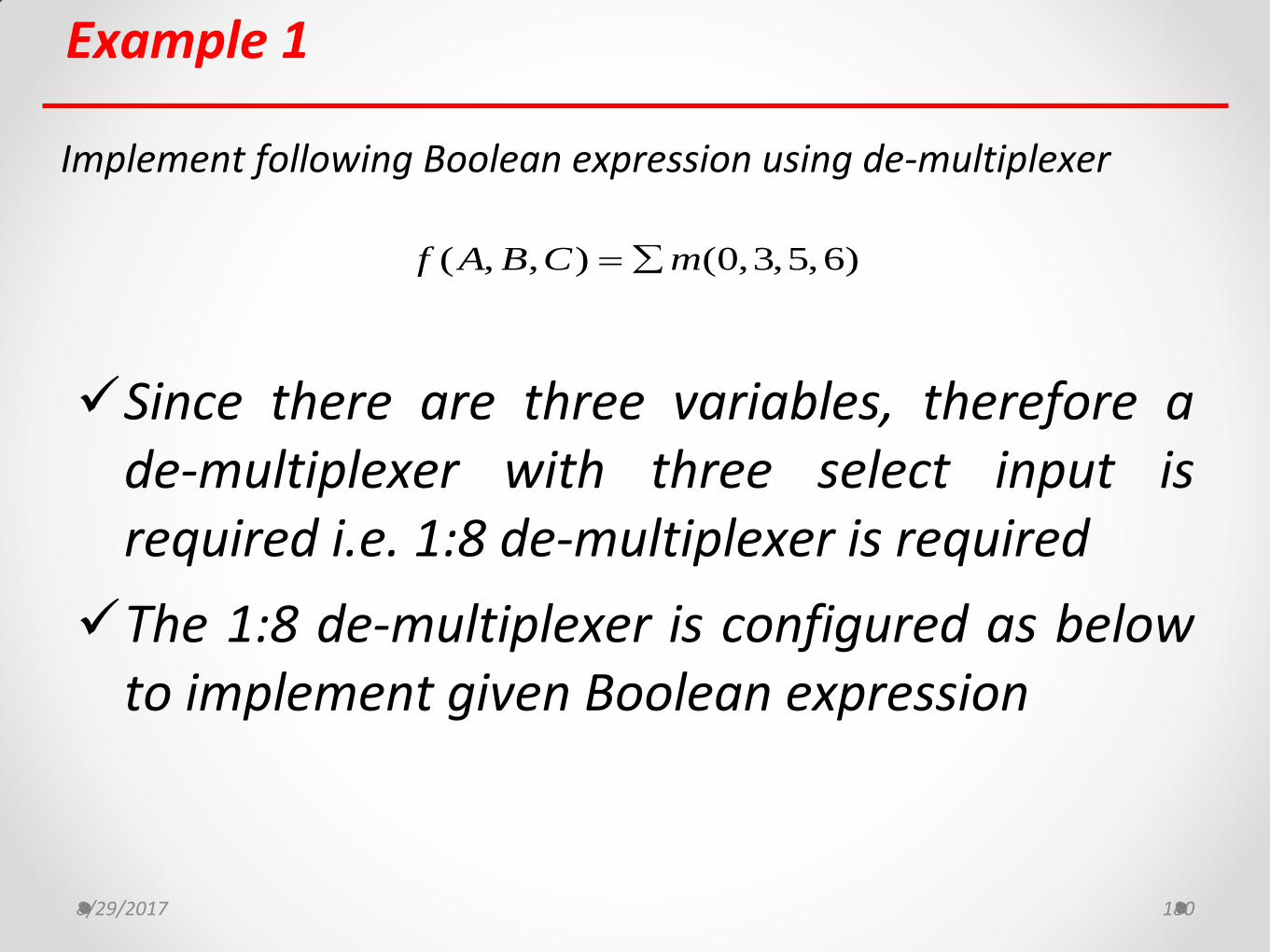
Implement following Boolean expression using de-multiplexer
Since there are three variables, therefore a de-multiplexer with three select input is required i.e. 1:8 de-multiplexer is required
The 1:8 de-multiplexer is configured as below to implement given Boolean expression
( , , ) (0,3,5,6)f A B C m
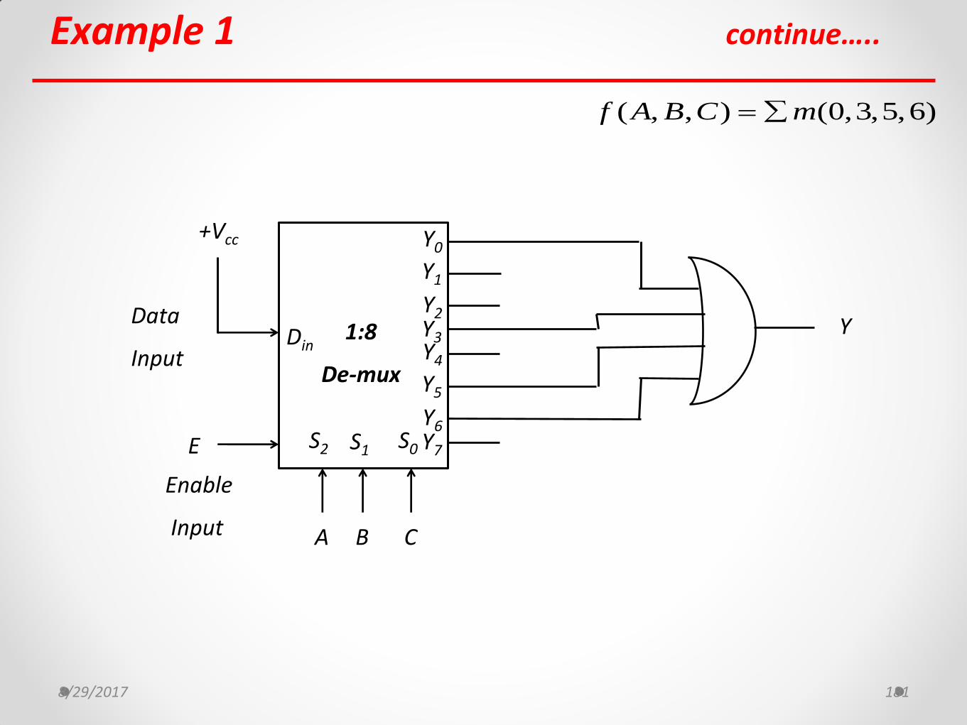
Example 1 continue…..
8/29/2017 181
+Vcc
1:8
De-mux
E
Enable
Input
Y0
Y1
Data
Input Din
S0 S1
Y2 Y3 Y4
Y5
Y6 Y7 S2
A B C
Y
( , , ) (0,3,5,6)f A B C m
Example 2
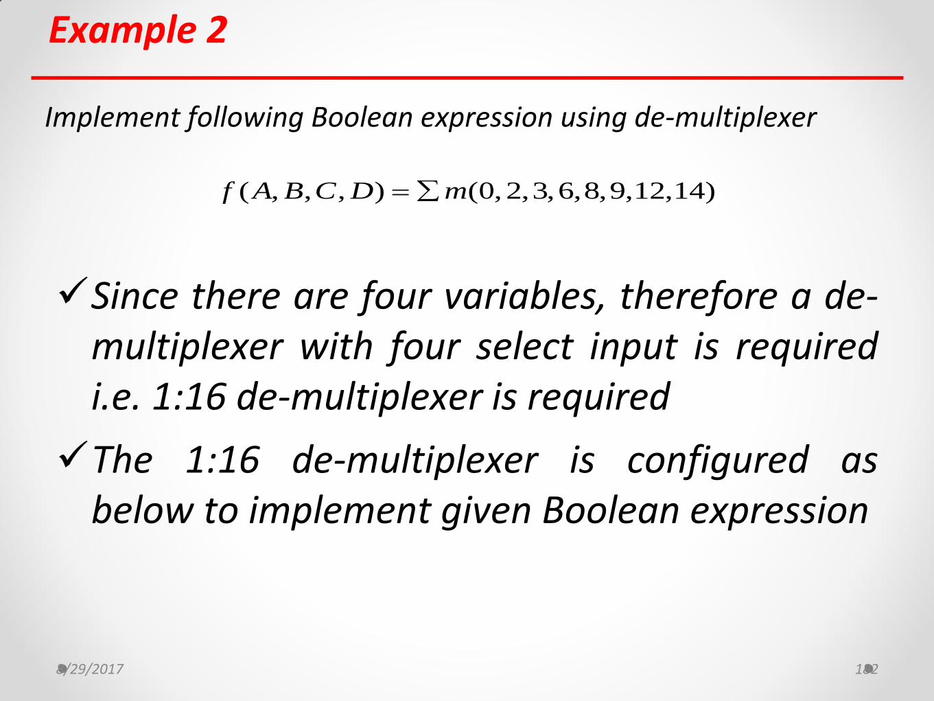
8/29/2017 182
Implement following Boolean expression using de-multiplexer
Since there are four variables, therefore a de-multiplexer with four select input is required i.e. 1:16 de-multiplexer is required
The 1:16 de-multiplexer is configured as below to implement given Boolean expression
( , , , ) (0,2,3,6,8,9,12,14)f A B C D m
Example 2 continue…..
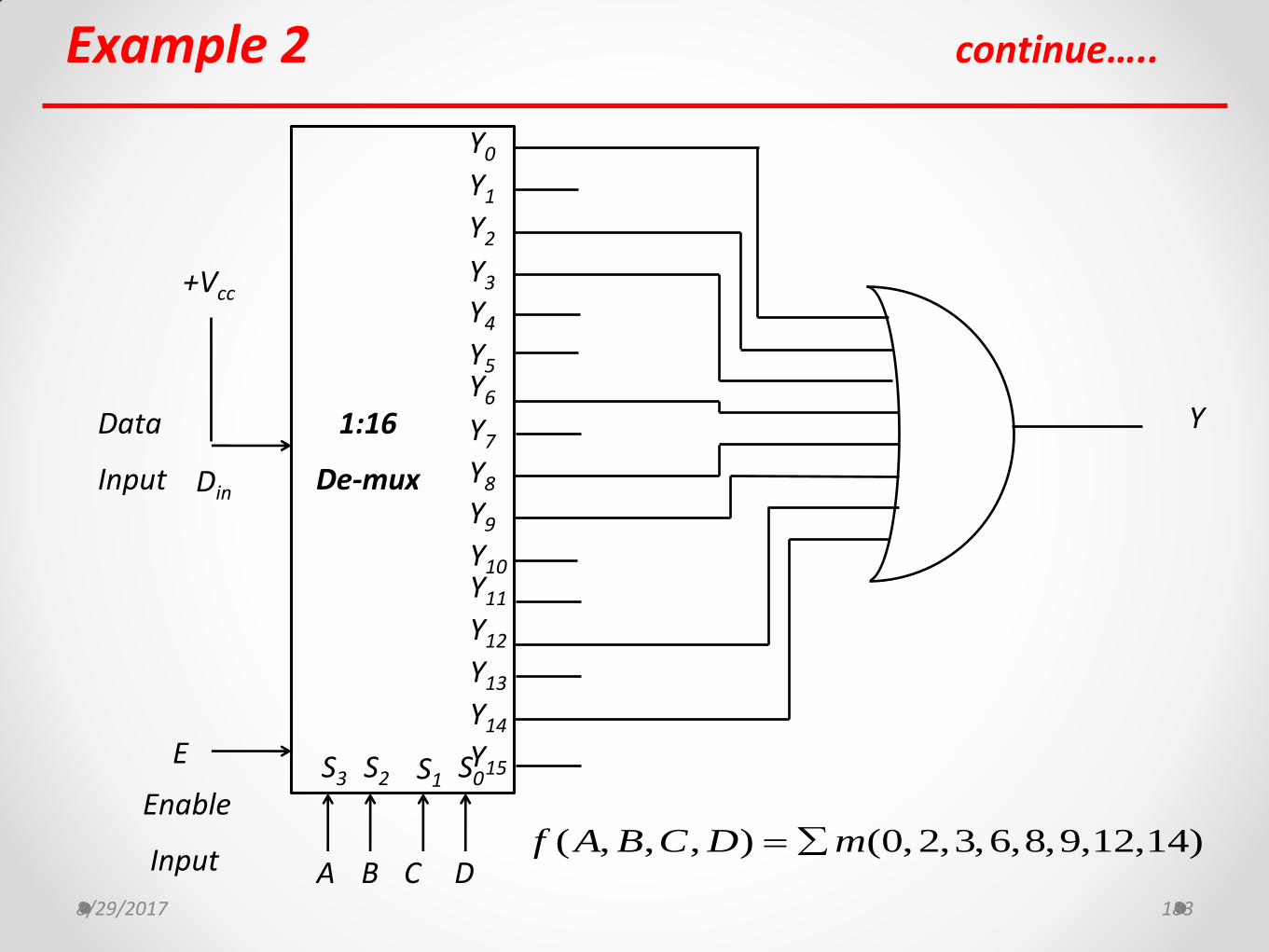
8/29/2017 183
A B C
+Vcc
D
1:16
De-mux
E
Enable
Input
Y0
Data
Input Din
S0 S1 S2
Y1
Y2
Y3
Y4
Y5 Y6
Y7
Y8
Y9
Y10 Y11
Y12
Y13
Y14
Y15 S3
Y
( , , , ) (0,2,3,6,8,9,12,14)f A B C D m
Module III – Combinational Logic Circuits
Necessity, Applications and Realization of following (8 Marks)
Multiplexers (MUX): MUX Tree
Demultiplexers (DEMUX): DEMUX Tree, DEMUX as Decoder
Study of IC 74151, IC 74155
Priority Encoder 8:3, Decimal to BCD Encoder
Tristate Logic, Unidirectional & Bidirectional buffer ICs: IC 74244 and IC 74245
8/29/2017 184
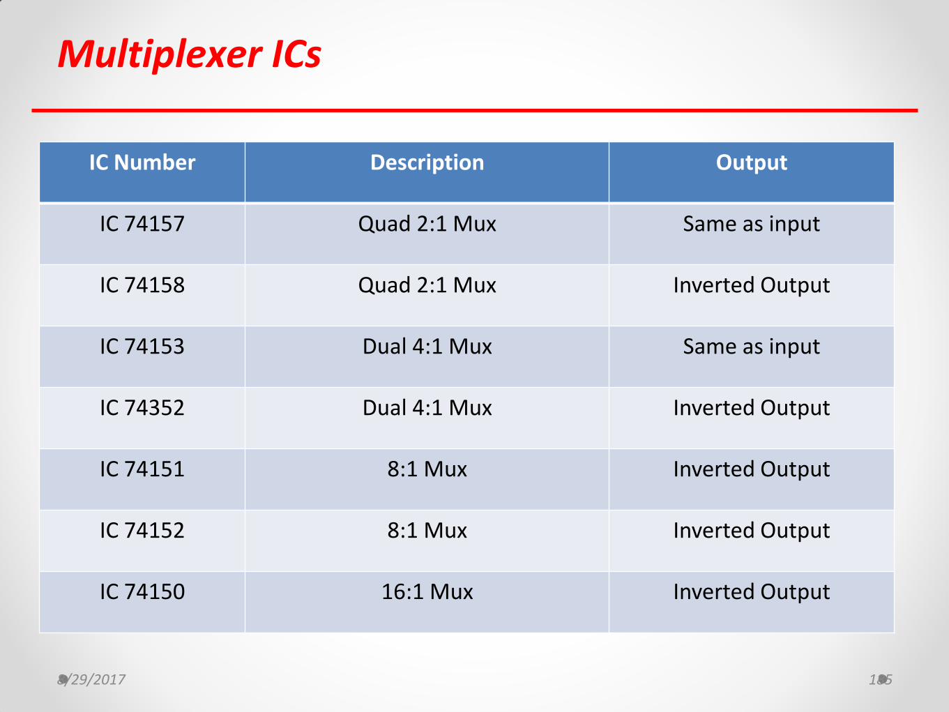
Multiplexer ICs
IC Number Description Output
IC 74157 Quad 2:1 Mux Same as input
IC 74158 Quad 2:1 Mux Inverted Output
IC 74153 Dual 4:1 Mux Same as input
IC 74352 Dual 4:1 Mux Inverted Output
IC 74151 8:1 Mux Inverted Output
IC 74152 8:1 Mux Inverted Output
IC 74150 16:1 Mux Inverted Output
8/29/2017 185

IC 74151 – General Description
This Data Selector/Multiplexer contains full on-chip decoding to select one-of-eight data sources as a result of a unique three-bit binary code at the Select inputs.
Two complementary outputs provide both inverting and non-inverting buffer operation.
A Strobe input is provided which, when at the high level, disables all data inputs and forces the Y output to the low state and the output to the high state.
The Select input buffers incorporate internal overlap features to ensure that select input changes do not cause invalid output transients.
8/29/2017 186
Y
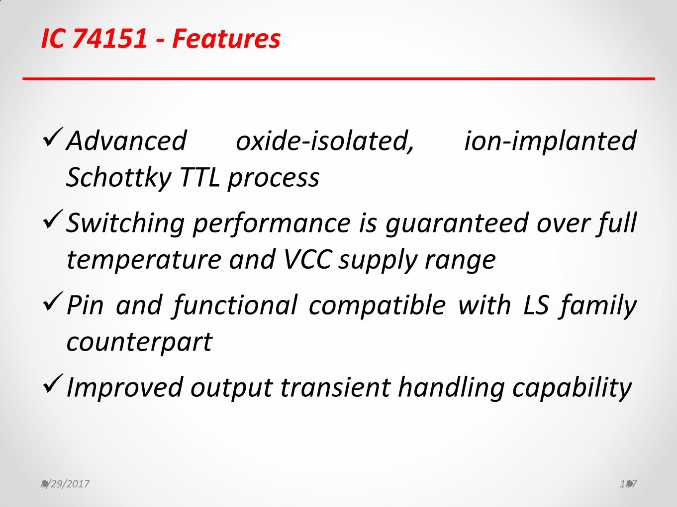
IC 74151 - Features
Advanced oxide-isolated, ion-implanted Schottky TTL process
Switching performance is guaranteed over full temperature and VCC supply range
Pin and functional compatible with LS family counterpart
Improved output transient handling capability
8/29/2017 187
IC 74151 – Pin Diagram
8/29/2017 188
Select Lines
8:1
Mux
Enable Input
Y
D0
D1
Data
Inputs
Equivalent Diagram
D2
D3
S0 S2
D4
D5
D6
D7
S1
VCC GND
Pin Diagram
E
Y
De-multiplexer ICs
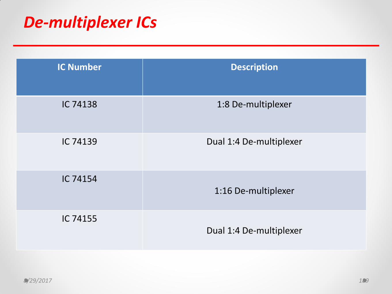
IC Number Description
IC 74138 1:8 De-multiplexer
IC 74139 Dual 1:4 De-multiplexer
IC 74154 1:16 De-multiplexer
IC 74155 Dual 1:4 De-multiplexer
8/29/2017 189

IC 74155 – General Description
These monolithic TTL circuits feature dual 1 line to 4 line de-multiplexers with individual strobes and common binary address inputs in a single 16 pin package.
The individual strobes permit activating or inhibiting each of the 4-bit sections as desired.
8/29/2017 190
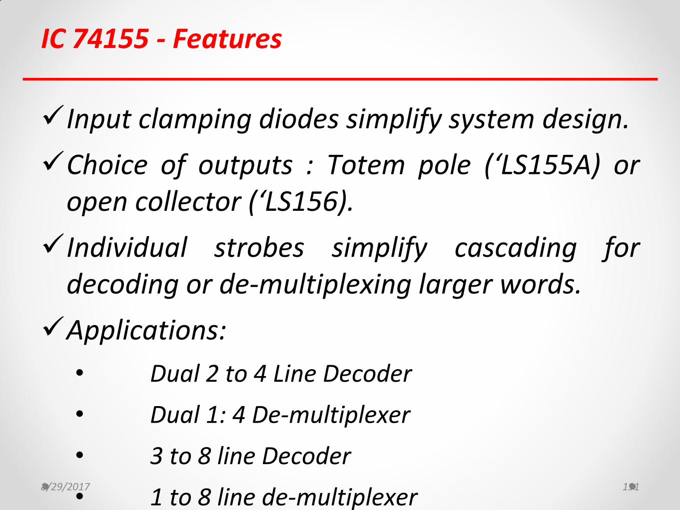
IC 74155 - Features
Input clamping diodes simplify system design.
Choice of outputs : Totem pole (‘LS155A) or open collector (‘LS156).
Individual strobes simplify cascading for decoding or de-multiplexing larger words.
Applications:
• Dual 2 to 4 Line Decoder
• Dual 1: 4 De-multiplexer
• 3 to 8 line Decoder
• 1 to 8 line de-multiplexer
8/29/2017 191
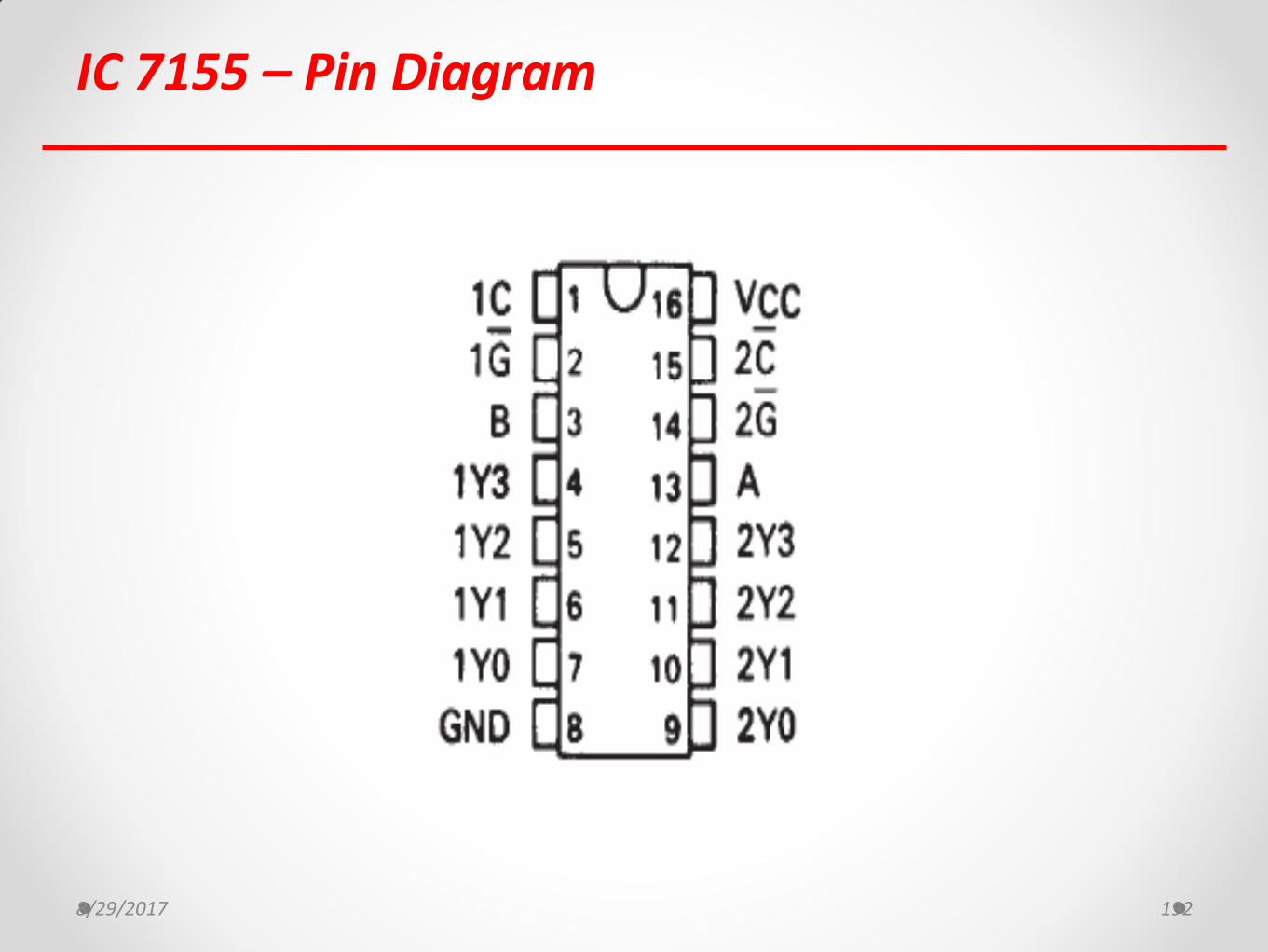
IC 7155 – Pin Diagram
8/29/2017 192
Combinational Logic Circuits
Necessity, Applications and Realization of following (8 Marks)
Multiplexers (MUX): MUX Tree
Demultiplexers (DEMUX): DEMUX Tree, DEMUX as Decoder
Study of IC 74151, IC 74155
Priority Encoder 8:3, Decimal to BCD Encoder
Tristate Logic, Unidirectional & Bidirectional buffer ICs: IC 74244 and IC 74245
8/29/2017 193
Encoder
Encoder is a combinational circuit which is designed to perform the inverse operation of decoder.
An encoder has ‘n’ number of input lines and ‘m’ number of output lines.
An encoder produces an m bit binary code corresponding to the digital input number.
The encoder accepts an n input digital word and converts it into m bit another digital word
8/29/2017 194
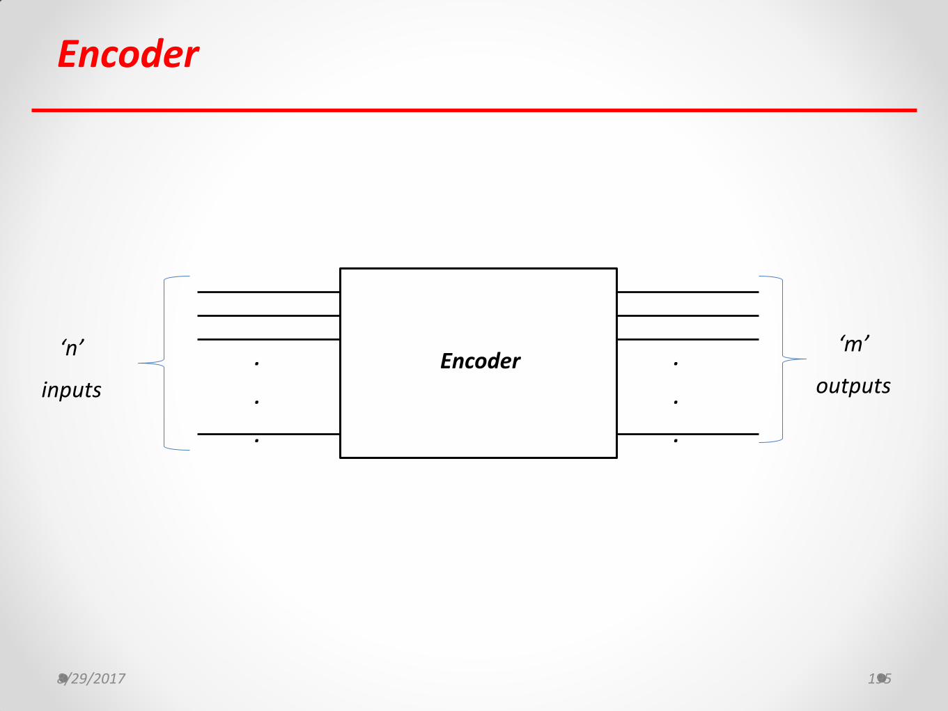
Encoder
8/29/2017 195
.
.
.
.
.
.
‘n’
inputs
‘m’
outputs Encoder
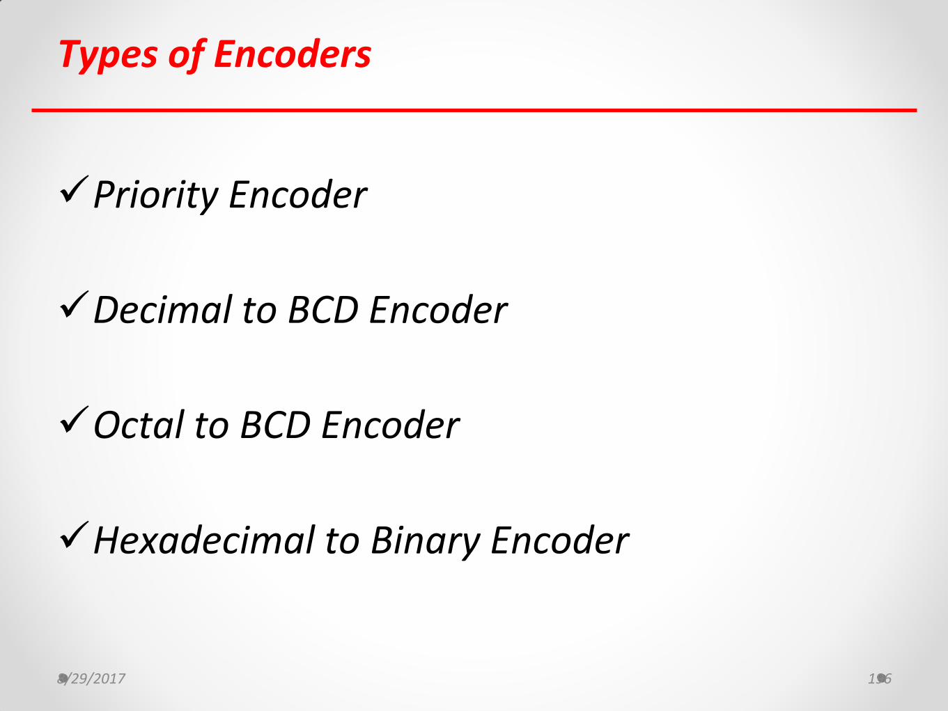
Types of Encoders
Priority Encoder
Decimal to BCD Encoder
Octal to BCD Encoder
Hexadecimal to Binary Encoder
8/29/2017 196
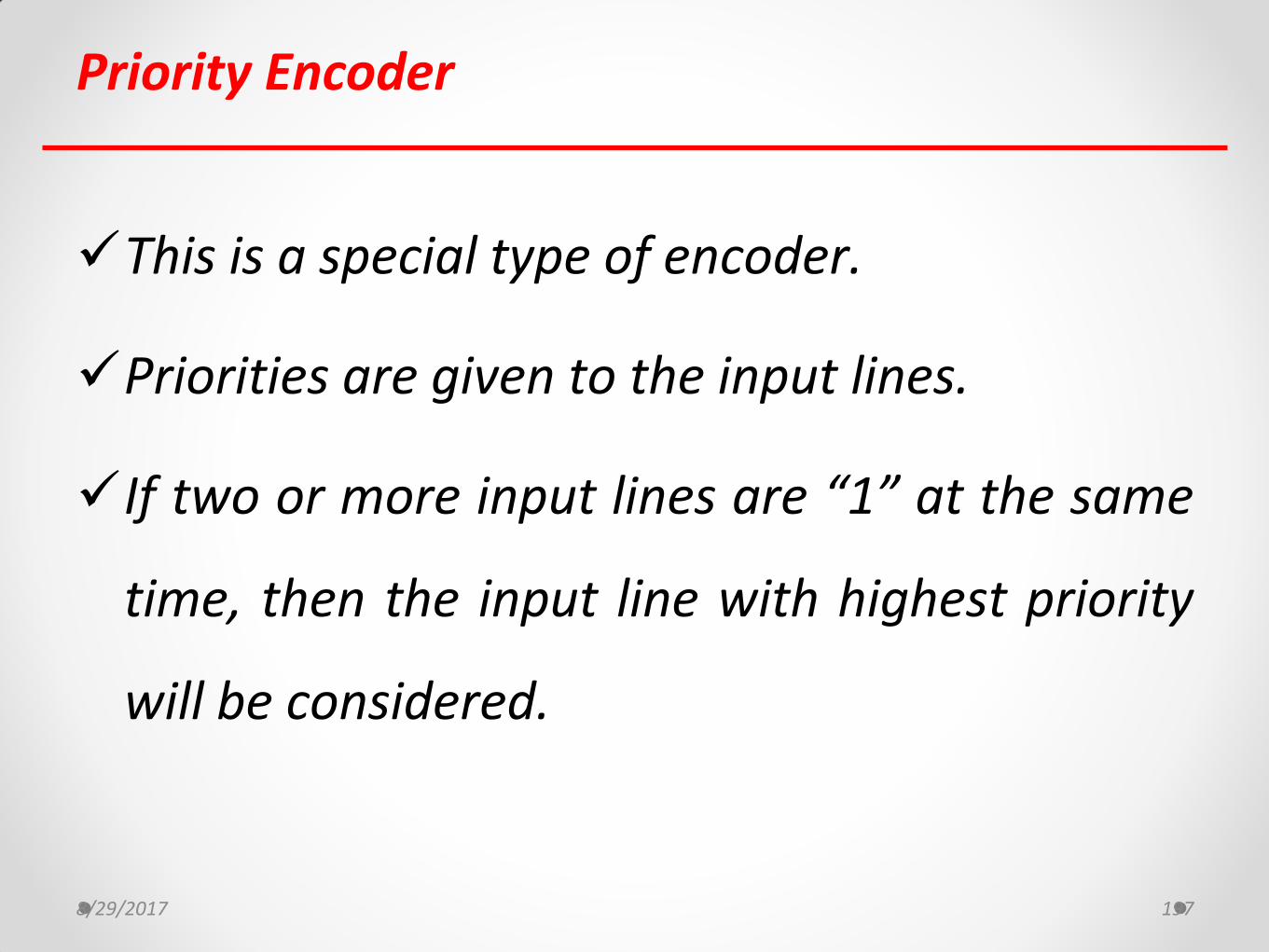
Priority Encoder
This is a special type of encoder.
Priorities are given to the input lines.
If two or more input lines are “1” at the same
time, then the input line with highest priority
will be considered.
8/29/2017 197
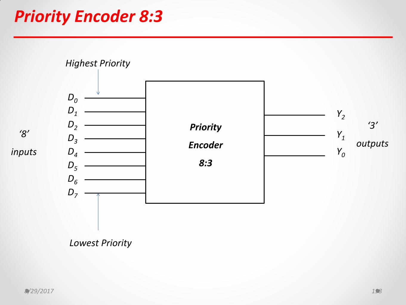
Priority Encoder 8:3
8/29/2017 198
‘8’
inputs
‘3’
outputs
Priority
Encoder
8:3
Y2
D0
D1
D2
D3
D4
D5
D6
D7
Y1
Y0
Highest Priority
Lowest Priority

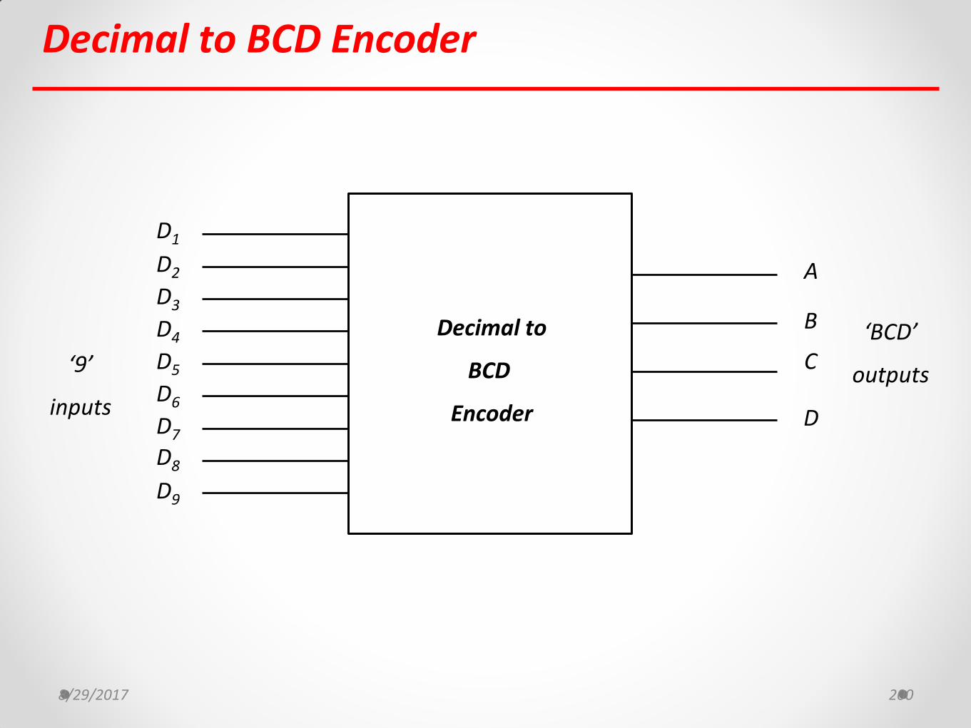
Decimal to BCD Encoder
8/29/2017 200
‘9’
inputs
‘BCD’
outputs
Decimal to
BCD
Encoder
A
D1
D2
D3
D4
D5
D6
D7
B
C
D8
D9
D

Combinational Logic Circuits
Necessity, Applications and Realization of following
Multiplexers (MUX): MUX Tree
Demultiplexers (DEMUX): DEMUX Tree, DEMUX as Decoder
Study of IC 74151, IC 74155
Priority Encoder 8:3, Decimal to BCD Encoder
Tristate Logic, Unidirectional & Bidirectional buffer ICs: IC 74244 and IC 74245
8/29/2017 201

Tristate Logic
In digital electronics three-state, tri-state, or 3-state logic allows an output port to assume a high impedance state in addition to the 0 and 1 logic levels, effectively removing the output from the circuit.
8/29/2017 202
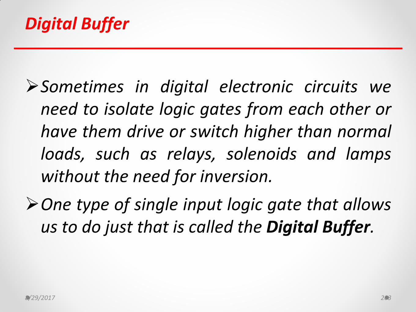
Digital Buffer
Sometimes in digital electronic circuits we need to isolate logic gates from each other or have them drive or switch higher than normal loads, such as relays, solenoids and lamps without the need for inversion.
One type of single input logic gate that allows us to do just that is called the Digital Buffer.
8/29/2017 203

Digital Buffer
Unlike the single input, single output inverter or NOT gate such as the TTL 7404 which inverts or complements its input signal on the output, the “Buffer” performs no inversion or decision making capabilities (like logic gates with two or more inputs) but instead produces an output which exactly matches that of its input. In other words, a digital buffer does nothing as its output state equals its input state.
Then digital buffers can be regarded as Idempotent gates applying Boole’s Idempotent Law because when an input passes through this device its value is not changed. So the digital buffer is a “non-inverting” device and will therefore give us the Boolean expression of: Q = A.
8/29/2017 204

Tri-state Buffer
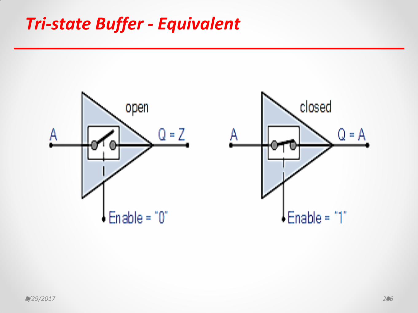
As well as the standard Digital Buffer seen above, there is another type of digital buffer circuit whose output can be “electronically” disconnected from its output circuitry when required. This type of Buffer is known as a 3-State Buffer or more commonly a Tri-state Buffer.
A Tri-state Buffer can be thought of as an input controlled switch with an output that can be electronically turned “ON” or “OFF” by means of an external “Control” or “Enable” ( EN ) signal input. This control signal can be either a logic “0” or a logic “1” type signal resulting in the Tri-state Buffer being in one state allowing its output to operate normally producing the required output or in another state were its output is blocked or disconnected.
8/29/2017 205
Tri-state Buffer - Equivalent
8/29/2017 206
What is Parity Generator? • A Parity Generator is a Combinational Logic Circuit that
Generates the Parity bit in the Transmitter.
• A Parity bit is used for the Purpose of Detecting Errors during
Transmissions of binary Information.
• It is an Extra bit Included with a binary Message to Make the
Number of 1’s either Odd or Even.

Two Types of Parity • In Even Parity, the added Parity bit will Make the Total
Number of 1’s an Even Amount.
• In Odd Parity, the added Parity bit will Make the Total
Number of 1’s an Odd Amount.
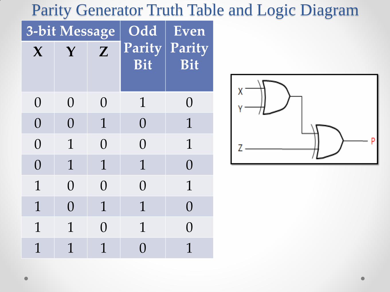
Parity Generator Truth Table and Logic Diagram
3-bit Message Odd Parity
Bit
Even Parity
Bit X Y Z
0 0 0 1 0
0 0 1 0 1
0 1 0 0 1
0 1 1 1 0
1 0 0 0 1
1 0 1 1 0
1 1 0 1 0
1 1 1 0 1
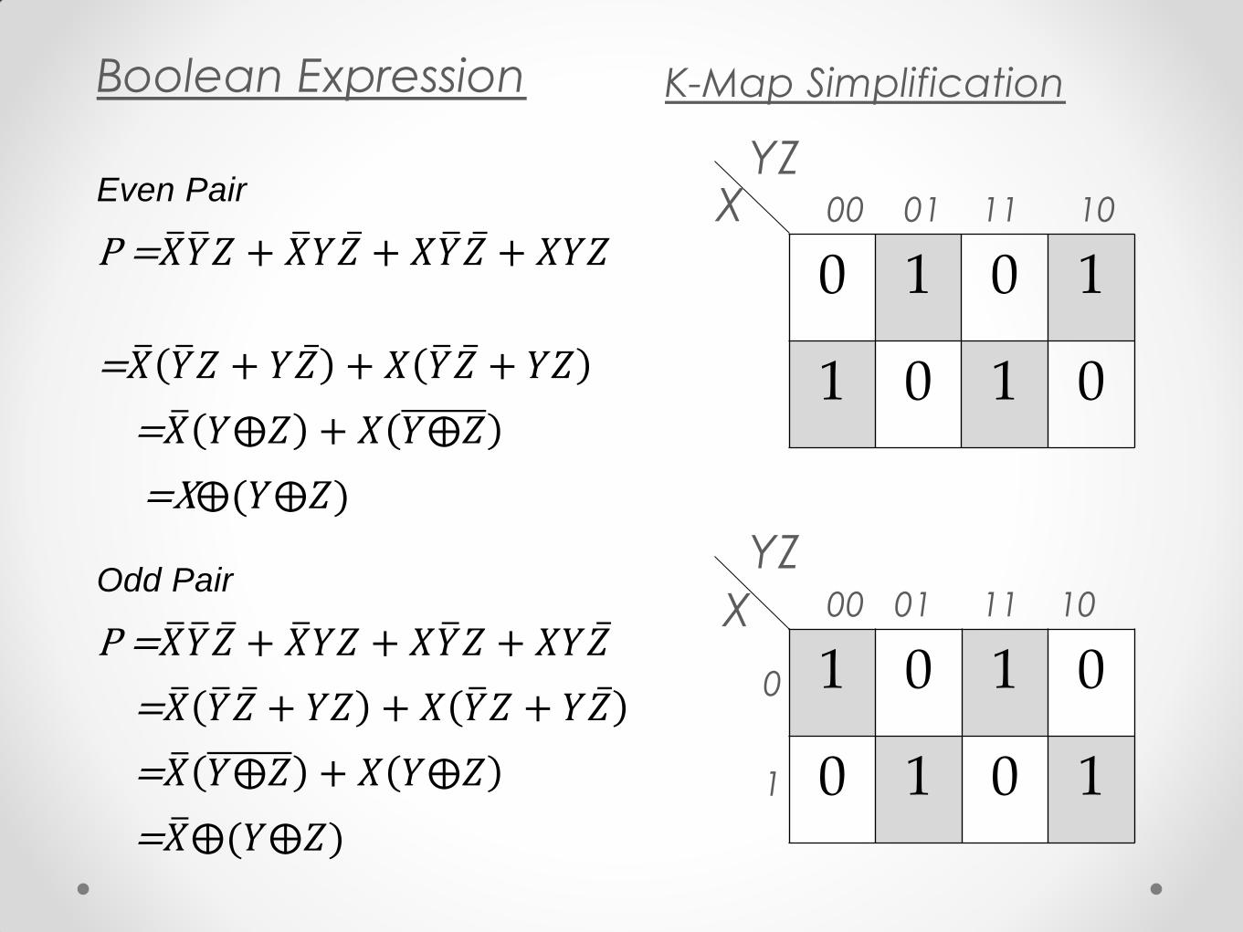
Even Pair
P =𝑋 𝑌 𝑍 + 𝑋 𝑌𝑍 + 𝑋𝑌 𝑍 + 𝑋𝑌𝑍
=𝑋 𝑌 𝑍 + 𝑌𝑍 + 𝑋 𝑌 𝑍 + 𝑌𝑍
=𝑋 𝑌⨁𝑍 + 𝑋 𝑌⨁𝑍
=X⨁(𝑌⨁𝑍)
0 1 0 1
1 0 1 0
X YZ
00 01 11 10
0
1
Boolean Expression K-Map Simplification
Odd Pair
P =𝑋 𝑌 𝑍 + 𝑋 𝑌𝑍 + 𝑋𝑌 𝑍 + 𝑋𝑌𝑍
=𝑋 𝑌 𝑍 + 𝑌𝑍 + 𝑋 𝑌 𝑍 + 𝑌𝑍
=𝑋 𝑌⨁𝑍 + 𝑋 𝑌⨁𝑍
=𝑋 ⨁(𝑌⨁𝑍)
1 0 1 0
0 1 0 1
X
YZ 00 01 11 10
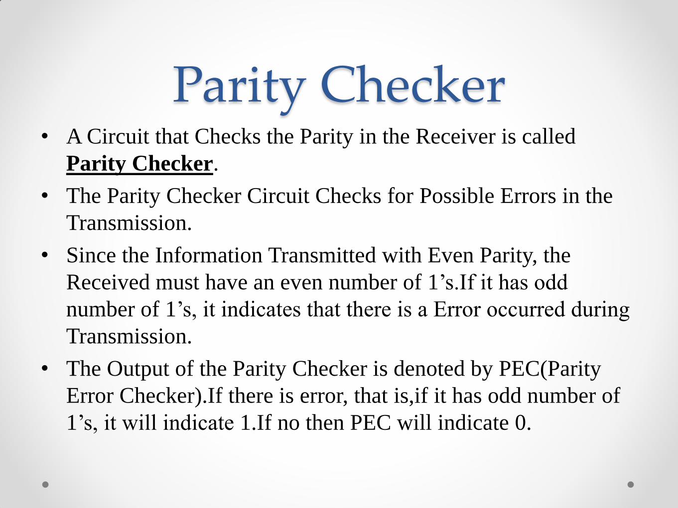
Parity Checker • A Circuit that Checks the Parity in the Receiver is called
Parity Checker.
• The Parity Checker Circuit Checks for Possible Errors in the
Transmission.
• Since the Information Transmitted with Even Parity, the
Received must have an even number of 1’s.If it has odd
number of 1’s, it indicates that there is a Error occurred during
Transmission.
• The Output of the Parity Checker is denoted by PEC(Parity
Error Checker).If there is error, that is,if it has odd number of
1’s, it will indicate 1.If no then PEC will indicate 0.
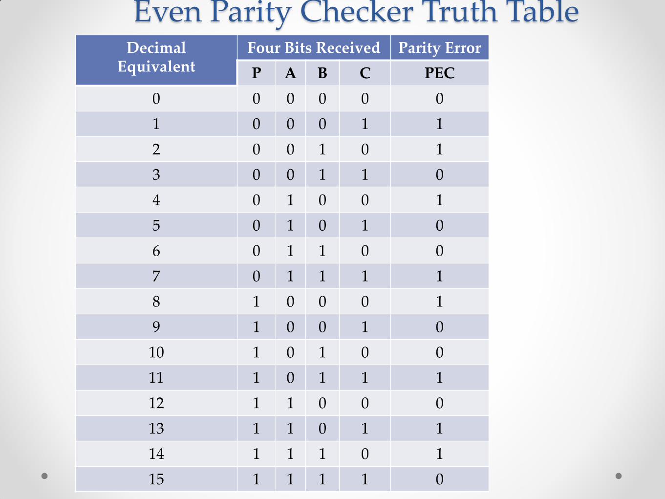
Decimal Equivalent
Four Bits Received Parity Error
P A B C PEC
0 0 0 0 0 0
1 0 0 0 1 1
2 0 0 1 0 1
3 0 0 1 1 0
4 0 1 0 0 1
5 0 1 0 1 0
6 0 1 1 0 0
7 0 1 1 1 1
8 1 0 0 0 1
9 1 0 0 1 0
10 1 0 1 0 0
11 1 0 1 1 1
12 1 1 0 0 0
13 1 1 0 1 1
14 1 1 1 0 1
15 1 1 1 1 0
Even Parity Checker Truth Table
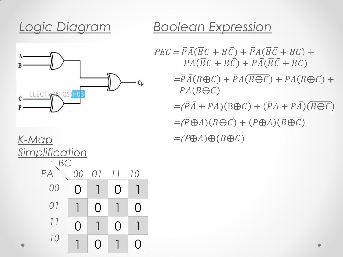
Logic Diagram Boolean Expression
PEC = 𝑃 𝐴 𝐵 𝐶 + 𝐵𝐶 + 𝑃 𝐴 𝐵 𝐶 + 𝐵𝐶 + 𝑃𝐴 𝐵 𝐶 + 𝐵𝐶 + 𝑃𝐴 (𝐵 𝐶 + 𝐵𝐶)
=𝑃 𝐴 𝐵⨁𝐶 + 𝑃 𝐴 𝐵⨁𝐶 + 𝑃𝐴 𝐵⨁𝐶 + 𝑃𝐴 𝐵⨁𝐶
=(𝑃 𝐴 + 𝑃𝐴) B⨁𝐶 + 𝑃 𝐴 + 𝑃𝐴 𝐵⨁𝐶
=(𝑃⨁𝐴) 𝐵⨁𝐶 + 𝑃⨁𝐴 𝐵⨁𝐶
=(P⨁𝐴)⨁(𝐵⨁𝐶) K-Map
Simplification
0 1 0 1
1 0 1 0
0 1 0 1
1 0 1 0
00 01 11 10
00
01
11
10
PA BC
Bi-directional Buffer
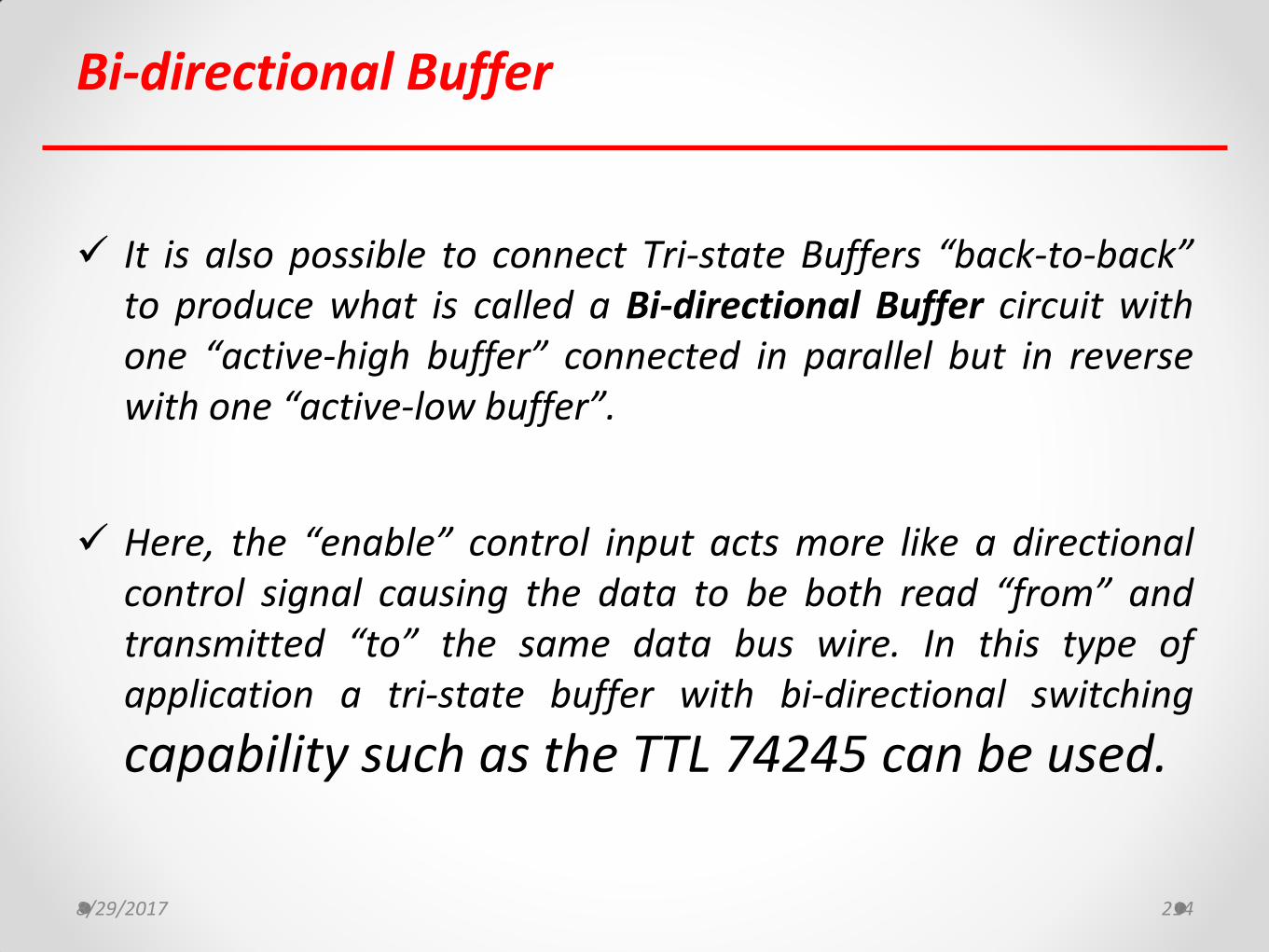
It is also possible to connect Tri-state Buffers “back-to-back” to produce what is called a Bi-directional Buffer circuit with one “active-high buffer” connected in parallel but in reverse with one “active-low buffer”.
Here, the “enable” control input acts more like a directional control signal causing the data to be both read “from” and transmitted “to” the same data bus wire. In this type of application a tri-state buffer with bi-directional switching
capability such as the TTL 74245 can be used.
8/29/2017 214
References
Digital Principles by Malvino Leach
Modern Digital Electronics by R.P. Jain
Digital Electronics, Principles and Integrated Circuits by Anil K. Maini
Digital Techniques by A. Anand Kumar
8/29/2017 215

Online Tutorials
http://nptel.ac.in/video.php?subjectId=117106086
http://www.electronics-tutorials.ws/combination/comb_1.html
http://www.electronics-tutorials.ws/combination/comb_2.html
8/29/2017 Amit Nevase 216

Thank You
8/29/2017 217