apollo study report, volume ii - ibiblio€¦ · · 2009-09-13apollo study report volume ii *•...
TRANSCRIPT
Apollo Study Report Volume
Machines N72-751112 (International Business1 Oct. 1963 36 p
VOLOMECorp.).
^

Apollo Study Report
Volume II
*• E. BOYES
RONGVED
"• L- WAGNER
Contract No. MAS 8-5296
and NAS 8-5276
CLASSIFICATION AND CONTENTS
APPROVED BY:
PROJECT OFFICE A P P R O V A L :
IBM NO.: 63-928-130
Prepared for the
GEORGE C. M A R S H A L L SPACE FLIGHT CENTER
Huntsvi l le, A labama
Space Guidance Center, Owego, New York
Technical Library, Bellcomm, Inc.1 October 1963

FOREWORD
The feasibility of adapting the Saturn V Guidance Computer, DataAdapter, and Laboratory Test Equipment to the Apollo application wasstudied by IBM under NASA Contract NAS 8-5296.
This report presents the results of the study effort. In order to publishthis report as soon as possible, it is being submitted without prior NASAreview. However, discussions with NASA personnel contributed significantlyto the compilation of this report. Volume I describes equipment that willsuccessfully fulfill the requirements of the Apollo mission. Volume n de-scribes the equipment currently being developed for Saturn V. The essentialsimilarities of Apollo and Saturn V equipment can provide significant timeand dollar savings during the Apollo development program.
11
*****
*****
*****
iii/iv

CONTENTS
Section Page
I. SYSTEM CONFIGURATION 1-1A. GENERAL 1-2B . SYSTEM BLOCK DIAGRAM . . 1-5C. MODES OF OPERATION 1-5
1. MODE 1 - GROUND CHECK-OUT. 1-72. MODE 2 - BOOST GUIDANCE 1-93. MODE 3 - ORBITAL CHECK-OUT 1-114. OTHER COMPUTATIONS 1-14
D. COMPUTER AND DATA ADAPTER CONSIDERATIONS . . 1-151. MEMORY STORAGE CAPACITY. 1-152. MEMORY STORAGE CHARACTERISTICS 1-153. COMPUTATIONAL SPEED 1-174. DATA ADAPTER DESIGN 1-17
II. RELIABILITY 2-1
IS. SATURN V COMPUTER , 3-1A. GENERAL DESCRIPTION 3-2B . COMPUTER FUNCTIONAL DESCRIPTION 3-7
1. CHARACTERISTICS 3-72. ORGANIZATION 3-93. TIMING 3-11
, C. COMPUTER CONTROL 3-131. INSTRUCTION LIST. 3-132. MULTIPLY AND DIVIDE TIMING 3-153. INTERRUPT 3-154. PROGRAMMING CONSIDERATIONS 3-16
D. ARITHMETIC SECTION 3-181. GENERAL 3-182. MULTIPLY 3-193. DIVIDE 3-20
E. MEMORY 3-23F. BASIC MEMORY SYSTEMS OPERATION 3-24G. COMPUTER INPUT/OUTPUT CAPABILITY 3-27
1. GENERAL 3-272. PIO INSTRUCTION 3-283. INTERRUPT. 0 3-28

Contents (cont)
Section Page
H. LOGIC CIRCUITS 3-281. DESIGN. 3-282. BASIC LOGIC CIRCUITS 3-29
I. SPECIAL CIRCUITS . 3-301. GENERAL 3-302. VOTER CIRCUIT 3-303. DISAGREEMENT DETECTOR 3-334. DELAY LINE CIRCUITS 3-335. CLOCK GENERATOR 3-34
J. TEMPERATURE CHARACTERISTICS 3-34K. COMPUTER PACKAGING AND ENVIRONMENTAL
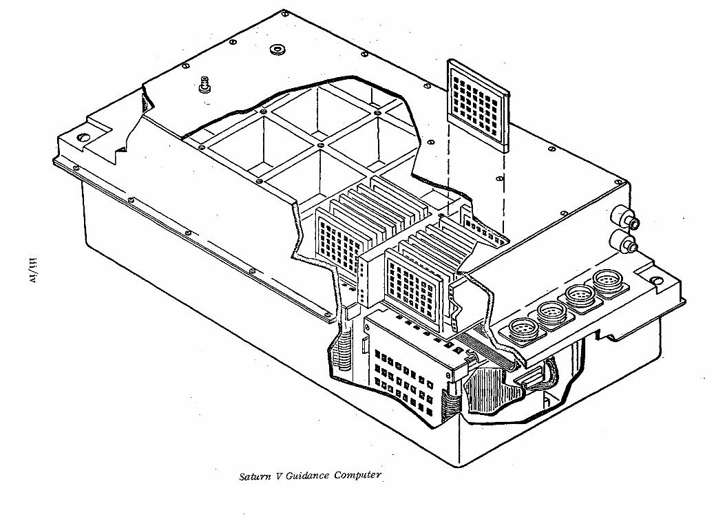
REQUIREMENTS 3-341. CONFIGURATION 3-342. MATERIAL 3-373. SEALING DESIGN < . 3-374. SIZE AND WEIGHT 3-375. COOLING 3-38
L. ENVIRONMENTAL REQUIREMENTS 3-39M. ELECTRONIC PACKAGING 3-40
1. UNIT LOGIC DEVICE (ULD) 3-402. MULTILAYER INTERCONNECTION BOARD (MIB) . 3-413. PAGE 3-414. BACK PANEL 3-435. MEMORY , 3-436., INTERCONNECTIONS 3-44
IV. SATURN V DATA ADAPTER 4-1A. GENERAL DESCRIPTION , 4-2B. FUNCTIONAL DESCRIPTION 4-5
1. DATA ADAPTER INTERNAL FUNCTIONS 4-52. POWER SUPPLIES 4-63. ADDRESS GENERATOR AND TAG REGISTER . . ..... 4-64. SWITCH SELECTOR REGISTER 4-75. DISCRETE OUTPUT REGISTER 4-76. DISCRETE INPUTS 4-87. SWITCH SELECTOR FEEDBACK INPUTS 4-88. INTERRUPT REGISTER 4-8
VI
Contents (cont)
Section Page
9. BUFFER REGISTER 4-910. MODE REGISTER 4-911. VALIDITY BIT GENERATOR 4-912. READY-BIT GENERATOR 4-1013. PARITY GENERATOR 4-1014. INTERNAL CONTROL DISCRETE REGISTER .. . . 4-1015. PIO DIGITAL INPUT MULTIPLEXER AND
SERIALIZER 4-1118. TMR DELAY LINE 4-li17. TELEMETRY MONITORING OF DATA 4-14
C. ANGLE MEASUREMENT 4-24D. POWER SUPPLY CONFIGURATION 4-25E. SPECIAL CIRCUIT DESIGN 4-28
1. 28-VOLT BUFFER INTERFACE CIRCUIT. 4-282. RESOLVER FREQUENCY SOURCE 4-28
, F. PACKAGING . 4-29
V. LABORATORY TEST EQUIPMENT 5-1A. GENERAL 5-2B. MACHINE CONFIGURATION 5-2C. DETAILED DESCRIPTION 5-3
1. ACME 5-32. ADAPT 5-83. ASTEC 5-94. ATOM 5-9
vii/viii

ILLUSTRATIONS
Figure Title Page
1-1 Guidance Subsystem 1-81-2 Apollo Vehicle S-V 1-81-3 Mode Flow Diagram 1-91-4 Boost Guidance 1-101-5 Orbital Check-out 1-12
II-1 Block Diagram of System Model 2-3
III-l TMR Voter Signal Outputs 3-6III-2 Saturn V Guidance Computer Simplified Diagram 3-8ni-3 Computer Timing 3-12III-4 MPY-DIV Timing Chart 3-16III-5 Self-Correcting Duplex-Toroid Memory System 3-26m-6 X-Y Coordinate Half-Select Current Error Detection . . . 3-27HI-7 INV Module 3-31in-8 AA Module 3-32III-9 Memory and Logic Assembly . 3-35111-10 Saturn V guidance Computer General Design 3-36IH-11 ULD Before and After Encapsulation . 3-42111-12 MIB Cross Section 3-43111-13 MIB Top Land Pattern . . 3-44111-14 MIB Circuit Layer 3-45IH-15 MIB Ground Plane 3-46111-16 MIB Front and Rear Before Trimming 3-47m-17 Page Mockup 3-48HI-IS, Memory Configuration 3-49HI-19 Flat Cable Artwork 3-50in-20 Computer Interconnection Wiring Diagram 3-51III-31 Interconnection System 3-52
IV-1 Saturn V Data Adapter Block Diagram 4-3IV-2 Use of Word. Locations 4-13IV-3 Proposed Digital Data Control for Telemetry
Transfers from the Saturn Data Adapter . . . '. 4-16IV-4 Data Adapter Telemetry. Timing 4-18IV-5 Angle Digitizer . 4-26
IX

Illustrations (Cont)
Figure Title Page
IV-6 Pulse-Width-Modulated Power Supply Module BlockDiagram 4-27
IV-7 Resolver Frequency Source-Block Diagram 4-28IV-8 Data Adapter Circuit Module 4-30IV-9 Data Adapter Packaging Layout 4-31/32
V-l ACME Installation Outline Drawing 5-4V-2 ADAPT Installation Outline Drawing 5-5V-3 ASTEC Installation Outline Drawing 5-6V-4 ATOM Installation Outline Drawing 5-7

TABLES
Table Page
1-1 STORAGE REQUIREMENT FOR COMPUTER 1-16
H-l NONREDUNDANT (SIMPLEX) MODE RELIABILITYWHEN OPERATING AT 100°C 2-6
II-2 REDUNDANT (DUPLEX) MODE RELIABILITY WHENOPERATING AT 100°C 2-7
II-3 NONREDUNDANT (SIMPLEX) MODE RELIABILITYWHEN OPERATING AT 75OC 2-8
II-4 REDUNDANT (DUPLEX) MODE RELIABILITYWHEN OPERATING AT 75°C 2-9
H-5 NONREDUNDANT (SIMPLEX) MODE RELIABILITYWHEN OPERATING AT 6QQC 2-10
II-6 NONREDUNDANT (DUPLEX) MODE RELIABILITYWHEN OPERATING AT 606C 2-11
II-7 SUMMARY OF SYSTEM RELIABILITYCALCULATIONS 2-12
III-l SATURN V COMPUTER CHARACTERISTICS 3-3m-2 TMR COMPUTER MODULE BREAKDOWN 3-4HI-3 DATA AND INSTRUCTION WORD FORMAT 3-10IH-4 OPERATION CODE MAP . . 3-13
IV-1 DATA ADAPTER CHARACTERISTICS 4-4IV-2 DEFINITION OF USE OF ADDRESS LINE BITS TO THE
DATA ADAPTER FOR PIO OPERATIONS 4-20IV-3 DEFINITION OF TAG CODE TO BE USED WITH
TELEMETRY 4-22
xi/xii

Section I
SYSTEM CONFIGURATION
1-1
Section I
SYSTEM CONFIGURATION
A. GENERAL
The Saturn V Guidance Computer and Data Adapter (DA) is inte-grated into the Saturn V vehicle guidance system. To meet the requirementsimposed by a variety of missions, flexible and highly reliable computer andDA equipment was designed. High computing speed and a random-accesscore memory are combined in a microminiature design approach achievinglow power dissipation and minimum size and weight.
The guidance computer is the primary computing element in the complexSaturn guidance system. It provides sufficient speed to meet all anticipatedcomputing needs and has a memory large enough to store all programs to beperformed in the various phases of the mission. The computer uses micro-miniature packaging technology, a random-access magnetic core memory,triple modular redundancy, and duplex memory modules to achieve the veryhigh reliability required for the Saturn missions. The computer isinterconnected with the DA which contains input and output conversionelectronics and power control equipment. The DA also connects the guidancecomputer with the ground control computer, the telemetry equipment, andthe guidance system sensors used during the mission.
High computational speed is obtained by operating the computer at a 500-kilocycle bit rate and using a logical organization that permits both additionand multiplication operations to take place simultaneously. Program in-structions are conserved in this mode of operation by allowing the pro-grammer control over whether one-word-time operations (and advancing ofthe instruction counter) are permitted during multiplication. One optionuses a multiply operation that allows concurrent one-word-time operations,while the other results in a sequential multiply mode by prohibiting one-word-time operations in the adder. Although this type of organization requires morecomponents than a machine organized to permit only sequential, nonconcur-rent operation, it allows a computational speed up to 40 percent greater thanthat of the conventional machine.
1-2

An instruction storage capacity of up to 32, 768 14-bit instructions (inthe duplex memory mode) is provided to store the programs associated withpre-launch check-out, injection guidance, orbital check-out and lunar tra- ,jectory injection. Data words, using two instruction words for a word lengthof 28 bits, may be intermixed with.instructions in any proportion. Eachword comprises two instructions or one data word. Memory modules maybe used singly or duplex in pairs, and up to eight magnetic core memorymodules of 4,096 words may be mounted in the computer.
The Saturn V Guidance Computer and DA can perform a variety of :(space booster and orbital missions, including injecting the Apollo lunarspacecraft into lunar trajectory. In view of the importance of these missions,the need to protect the lives of the astronauts involved, the expense of thevehicles, and the safety of launch equipment, reliability is of paramountimportance. For maximum reliability, triple modular redundancy (TMR) isused in the central computer electronics. The highly reliable central com-puter may then be used to provide for the reading of memory, the use of theinput/output instrumentation, and for operation of system check-out functionswith a high probability of having no malfunction in the vital central computer.TMR subdivides the computer logic into modules; the modules are triplicatedand a voter establishes an output based on a majority decision. One of themodules in each trio may fail (and in some circumstances, more than one),and the computer will continue to function.
The Saturn V DA contains power supplies for itself and for the computerand its memories. It also contains all input/output (I/O) equipment necessaryfor communication between the guidance system and the Instrument Unit sen-sors and telemetry equipment. It provides registers and sampling circuitsfor discrete outputs and inputs, including error monitoring of the computerand data adapter. A delay line buffers interrupt signals, which cause normalcomputer processing to stop, so that a high priority function may be handled. Astorage register also holds information intended for the RCA-110 GroundControl Computer, telemetry transmitter, and orbital check-out systemComputer Interface Unit (CIU). Gating circuits are provided for systeminputs from the RCA-110, command receiver, and CIU. Analog-to-digitalcircuits convert two-speed resolver inputs to digital form. (The resolversindicate platform gimbal angles, horizon scanner sensor angles, and otherangular inputs.) Optisyn inputs indicate velocity from the accelerometers.Ladder networks convert digital attitude error and other information to analogform.
The computer memory is organized to permit either simplex or duplexoperation. In simplex operation, the memory module to be used is specified,and reading and writing takes place in this module only. For duplex oper-ation, memory modules are used in pairs with identical information stored in
1-3
each member of the pair. Each memory is read out, but information fromonly one of them is used. If checking shows the information to be in error,the other memory output is used. Verified information is simultaneouslywritten into both memories. This duplexing provides a very high reliabilitymemory system, which is able to correct errors by its unique employmentof two memory modules. Noncritical portions of the mission, such as groundpre-launch check-out, may be carried out using a simplex memory con-figuration. Where very high reliability is required during the flight, duplexmemory operation would be used; thus, duplex memory organization provideslarge capacity during short and noncritical mission phases and less capacityand greater reliability for long and critical mission phases. The DA alsocontains redundant features for high reliability.
Redundancy leads to unique possibilities for the maintenance of thecomputer and DA. Each channel of the TMR central computer can be oper-ated in turn under control of data adapter relays. Simple test problems thenindicate whether the channel is functioning properly. The ground equipmentcan also switch modules in the TMR configuration to determine if individualmodules (of which each simplex channel has seven) are malfunctioning. Theinputs to the voters used in the TMR logic are monitored to determine whenthey do not agree. The disagreement detectors associated with each page oflogic are OR'd together to isolate malfunctions to a trio of triplicated pages.In a like manner, two duplexed logic functions may be compared for disa-greement and test programs and special detection circuits used to localizemalfunctions. Parity checking is used in the memories to detect readingand writing errors. Addressing currents are monitored to ensure that theyare within specified magnitude and timing limits. Test programs are usedto periodically check memory operation.
The Saturn V Computer Manual Exerciser (ACME) laboratory test equip-ment was designed to test the guidance computer. It contains data displays,memory loading and verification, a test stand for mounting the computerduring test, and can exercise the computer-DA interface for testing. TheSaturn V Data Adapter Processor Tester (ADAPT) tester performs similarfunctions for the DA. It can also exercise the interfaces between the DA andexternal sensors.
ASTEC laboratory test equipment can test either the computer or theDA in the same manner as the ACME and the ADAPT testers. The Saturn VTest and Evaluation Console (ASTEC) can also test the combined computer-DA,using a computer test program. Other functions of the ASTEC include thecapability to check operational programs by simulating system inputs in realtime and recording computer and DA outputs. In addition, it can assist indiagnosing of prime equipment malfunctions by analyzing information avail-able at test points and automating the check-out procedure.
1-4

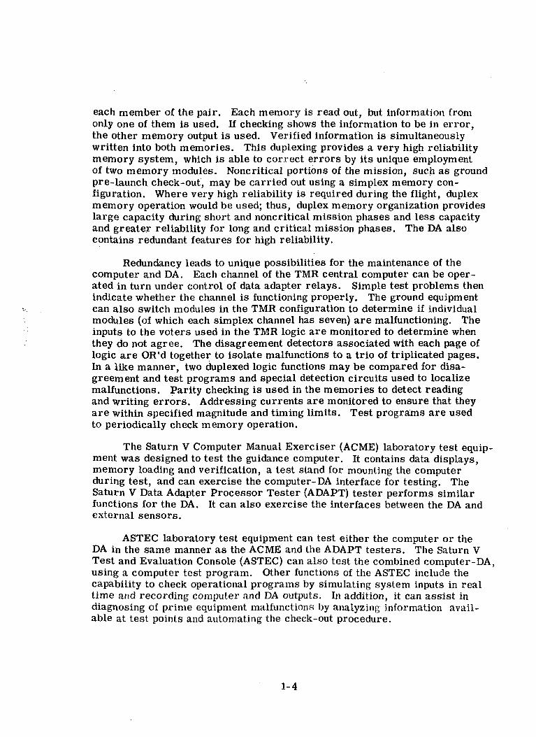
B. SYSTEM BLOCK DIAGRAM
The Saturn V Guidance System consists of the equipment shown in Fig-ure 1-1. The DA is the focal point for interfaces among system equipment.It interconnects with input sensors, ground command and telemetry equipment,ground support and checkout equipment, and the guidance computer. The DAalso contains analog-to-digital and digital-to-analog converters, power sup-plies and voltage sequencing, mode switching, and telemetry addressing.
The guidance computer, with its associated memory units, intercon-nects with the DA to perform all the required computation in the guidancesystem. The computer, through the use of an I/O instruction in its ordercode, controls the interchange of information between computer and the DA.The PIO instruction transfers one data word between the accumulator ormemory and the DA.
The computer-DA interface consists of signal and control lines ofvarious types. Computer timing signals are supplied to the DA to synchronizeI/O quantities. Eight lines select the I/O device or circuit in the DA fromwhich a computer input is read or to which a computer output is delivered.The devices or circuits include delay lines, counters, and static signalbuffers. An additional control line indicates whether an input or an outputfunction is to be performed. A computer interrupt signal consisting of dis-crete inputs OR'd together permits external signaling and interruption of theprogram both for normal mission operation and for operation with groundcheck-out equipment. A timed interrupt is also generated within the DA.
Computer starting and initialization are controlled by computer-DAinterconnections. I/O data are serialized and transmitted to and from theDA over single I/O lines. The DA interprets the equipment selection signaland directs the data to the proper location. Discrete inputs and outputs arecombined into words and handled like other I/O data. The flexibilityof the computer-DA interface and the operation codes provided permit a widevariety of input and output devices to be attached as dictated by variousmission requirements.
C. MODES OF OPERATION
To assist in establishing computer speed and storage requirements andto define typical mission I/O functions, which must be handled for a Saturn Vapplication, four operating modes or states have been outlined. Some of-thesemodes contain major submodes which are significant within themselves, butthe list has been restricted for preliminary consideration. Throughout thediscussion of the modes, the guidance computer is assumed to be mounted inthe main Apollo mission booster.
1-5
VEHICLEBATTERY
TELEMETRYTRANSMITTER
DISCRETEINPUTS aOUTPUTS
28V DC
GUIDANCECOMPUTERLOOIC ANDMEMORYUNITS
DATA
CONTROL
TIMING
.DATAADAPTER
ACCELEROMETERS
GIMBAL ANGLES
rrnPLATFORMST-124
DATA
(40)
RCA-110
SERVOUNIT
HORIZONSCANNER
GIMBAL ANGLES
Figure 1-1. Guidance Subsystem
1-6
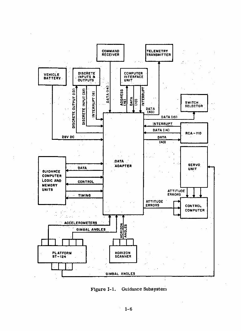
The guidance computer is placed at the top of those propulsion systemswhich are responsible for carrying a "payload" into orbit. In the Apolloconfiguration, shown in Figure 1-2, the first two stages are used to boost thesystems above stage two into an earth orbit. The third stage injects thedevices attached above it into a lunar transfer trajectory. The third stage isdiscarded after the lunar injection burning is completed; thus the computerhas completed its functions at that point. Lunar orbit rendezvous of theApollo spacecraft and a lunar excursion module is assumed.
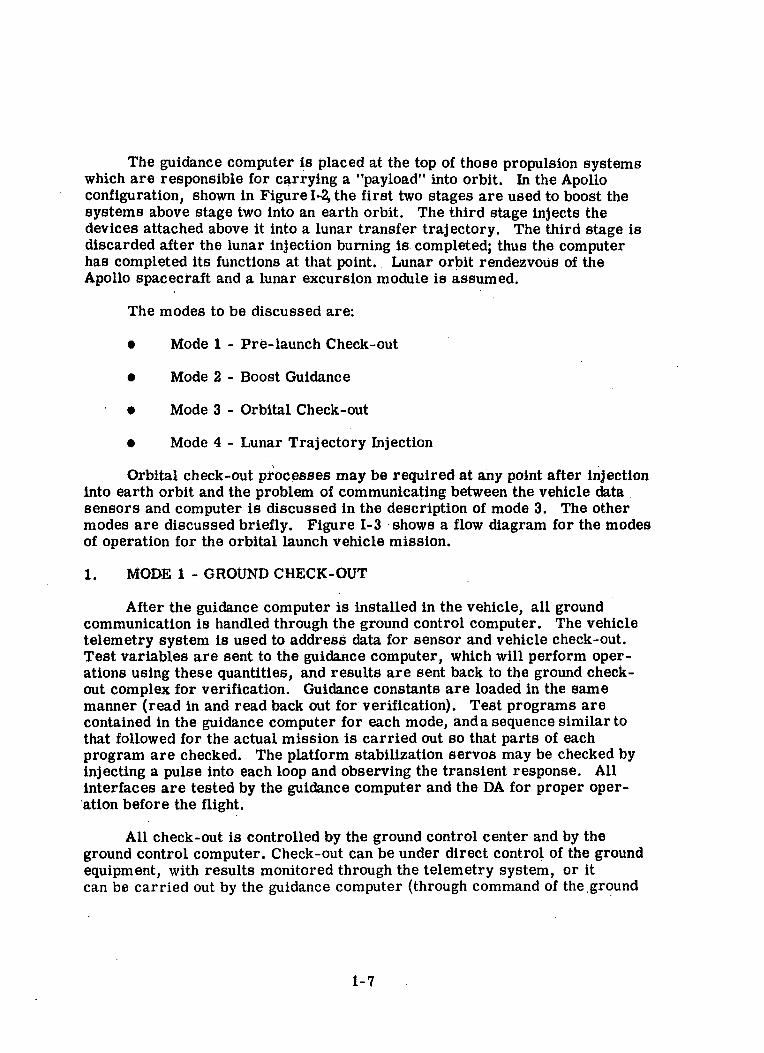
The modes to be discussed are:
• Mode 1 - Pre-launch Check-out
• Mode 2 - Boost Guidance
• Mode 3 - Orbital Check-out
• Mode 4 - Lunar Trajectory Injection
Orbital check-out processes may be required at any point after injectioninto earth orbit and the problem of communicating between the vehicle datasensors and computer is discussed in the description of mode 3. The othermodes are discussed briefly. Figure 1-3 shows a flow diagram for the modesof operation for the orbital launch vehicle mission.
1. MODE 1 - GROUND CHECK-OUT
After the guidance computer is installed in the vehicle, all groundcommunication is handled through the ground control computer. The vehicletelemetry system is used to address data for sensor and vehicle check-out.Test variables are sent to the guidance computer, which will perform oper-ations using these quantities, and results are sent back to the ground check-out complex for verification. Guidance constants are loaded in the samemanner (read in and read back out for verification). Test programs arecontained in the guidance computer for each mode, and a sequence similar tothat followed for the actual mission is carried out so that parts of eachprogram are checked. The platform stabilization servos may be checked byinjecting a pulse into each loop and observing the transient response. Allinterfaces are tested by the guidance computer and the DA for proper oper-ation before the flight.
All check-out is controlled by the ground control center and by theground control computer. Check-out can be under direct control of the groundequipment, with results monitored through the telemetry system, or itcan be carried out by the guidance computer (through command of the.ground
1-7

:AFTEARTHRETURNROCKET
LUNAR EXCURSIONMODULE
BOOSTER H/= =
ADVANCED SATURNIN8TRUMENTUNIT
BOOSTER i = = =
AN APOLLO ASSEMBLY
Figure 1-2. Apollo Vehicle S-V
1-8
START
MODE 1
PRELAUNCH CHECKOUTPROGRAM CHECKCOEFFICIENT LOAD
MODE 2
BOOST GUIDANCESTEERING COMMANDSENGINE CONTROL
MODE 3
ORBITAL CHECKOUTOVERALL SPACEVEHICLE TEST
MODE 4
LUNAR TRAJECTORY INJECTIONSTEERING COMMANDSENGINE CONTROL
FINISH
Figure 1-3. Mode Flow Diagram
control computer) and results sent to the ground. The routines performedconsist of Load, Verify, and Test Launch Constants; Computer Self-Test;Self-Contained Mission Simulation; System Test; Mode Control; InertialElement Performance Monitor; Telemetry Check; Delayed Launch ConditionComputation; and Delayed Launch Coefficient Modification.
2. MODE 2 - BOOST GUIDANCE
During the period from liftoff to burnout of the final boost stage thecomputer inputs and outputs consist of the following (Figure 1-4):
(a) Inputs
• Accelerometer outputs, in the form of optisyn encoders,representing velocity.
• Discrete inputs indicating liftoff, stage 1 cutoff, separation,stage 2 ignition, stage 2 'cutoff, engine out, etc.
1-9

VEHICLEBATTERY
DISCRETEINPUTS aOUTPUTS
Z8V DC
TELEMETRYTRANSMITTER
GUIDANCECOMPUTERLOGIC ANDMEMORYUNITS
DATA
CONTROL
TIMING
DATAADAPTER
ACCELEROMETERS
GIMBAL ANGLES
DATA SWITCHSELECTOR
DATA
SERVOUNIT
ATTITUDEERRORS , ,
ATTITUDEERRORS ' CONTROL
COMPUTER
rrnPLATFORMST-134
LIGIMBAL ANGLES
Figure 1-4. Boost Guidance
1-10

• Platform gimbal angles in the form of two-speed resolver signals,
(b) Outputs
• Attitude error signals, which are resolved in computer.
• Telemetry data words, at a maximum rate of 240 per second,to monitor computer and DA operation.
• Discrete outputs commanding second and third stage cutoff,stage separation, etc.
The computer routines executed during the boost guidance mode consistof the following:
i Navigation - the velocity vector is determined, coordinate trans-formation is performed, present position is calculated, and thegravity vector is projected into the guidance coordinate frame.
• Steering - Projections of required velocity are computed througha polynomial path-adaptive scheme, and steering commands arecomputed.
• Logic - Timed vehicle functions and logical decisions are made.
• Cutoff - A polynomial is used to compute cutoff time.
• Reasonableness Testing - All navigation and steering parametersare checked for reasonableness.
Corrections resulting from gyro drift-rate data are carried out in thismode if necessary.
Computations in Mode 4, Lunar Transfer Trajectory Injection, aresimilar to this mode.
3. MODE 3 - ORBITAL CHECK-OUT (See Figure 1-5)
The Saturn V computer is needed to check out all vehicle systems whilein orbit, prior to launching the Apollo spacecraft into a lunar trajectory.This is the last point at which the operational capability of the system can bechecked and an abort initiated before the spacecraft is committed to its tripto the moon. Propulsion, attitude control, radio command, guidance,telemetry, and radar systems require check-out. The Saturn InstrumentUnit must also be checked out. These systems are activated to the greatest
1-11

INSTRUMENT UNIT aVEHICLE MEASUREMENTS
COMMANDRECEIVER
DATA
VEHICLEBATTERY
28V DC
GUIDANCECOMPUTERLOQlC ANDMEMORYUNITS
DATA
CONTROL
TIMING
DATAADAPTER
GIMBAL ANGLES
DATA
SERVO
ATTITUDEERRORS
PLATFORMST-124
Figure 1-5. Orbital Check-out
1-12
extent possible and the computer sequentially initiates stimuli to each systemand evaluates its response via feedback from the telemetry analog-to-digitalconverter. The computer is able to identify the telemetry data and has go,no-go limits stored for each parameter it monitors as well as certain dynamicresponse characteristics. Up to 2,000 different parameters are evaluatedeither statically, dynamically, or both.
When dynamic response is checked, a few standard characteristicequations can be stored in the computer, with sets of reference coefficientsfor the various parameters being tested. One of the major reasons forperforming the orbital checkout is to save telemetry power, so only theresults of the tests are transmitted to the ground. Since the tests mightbe performed while the vehicle is in an unfavorable orientation or locationfor telemetry transmission, there is a need to store and transmit, at a latertime, certain test results and selected data which were questionable and re-quired further analysis on the ground.
Data Adapter inputs and outputs during this mode are as follows:
(a) Inputs
• Platform gimbal angles in the form of two-speed resolver signals.
• Quantities measured through the telemetry multiplexer and Com-puter Interface Unit, which are checked in the computer.
• Commands and data from the command receiver.
• Discrete inputs indicating status of Instrument Unit and vehicleequipment and responses to tests performed.
(b) Outputs
• Attitude error signals which were resolved in computer.
• Telemetry data words, at a maximum rate of 240 per second,to monitor computer and DA operation, and report orbitalcheck-out information to the ground.
• Discrete outputs to initiate tests and stimuli to IU and vehicleequipment.
• Address information to the Computer Interface Unit to selectquantities for checking.
1-13

4. OTHER COMPUTATIONS
In addition to the basic modes of operation and computations previouslyoutlined, certain other computations, described in the following paragraphs,must logically be performed by the on-board computer in the orbital launchvehicle.
Load and Verify Data - Data from the vehicle radio command system areloaded in the computer memory and verified. Synchronization signals mustbe properly decoded and precautions taken to ensure that the correct memorylocations are used.
Malfunction Isolation Tests - When a malfunction in the vehicle system isdetected, several alternate means of handling it are available. The airbornecomputer can be placed under control of the ground control complex to carryout detailed commands within the system; the ground control computer canload appropriate test routines into the memory of the airborne computer,which would then carry out the testing functions; or the test routines can bestored in the airborne computer memory, and carried out on command fromthe ground. These tests are very extensive, particularly in the case ofredundant equipment where the malfunctioning element must be identified.These tests also include decisions which initiate alternate modes of operationwhere other inputs are available.
Data Transmission - A special routine is used to transmit selected data duringcheckout modes or during certain other modes of operation. This data is inaddition to normally-transmitted flight data.
Computer Self-Test - A portion of each routine is devoted to computer self-test. This testing continuously monitors computer performance, and is inaddition to a pre-flight test routine.
DA Test - The computer conducts tests to indicate the performance of the DAand to localize malfunctions. The DA delay lines are written into and readfrom. Sample quantities are converted through the ladder decoders to testtheir operation. If duplexed logic outputs do not agree,tests are originatedtolocalize the malfunction to either one of the pair.
Other Mission Equations - Numerous other programs are part of the com-puter requirements for various space booster missions. For example,practice rendezvous missions are executed in earth orbit to test all systemsand operational concepts before attempting a lunar orbit rendezvous.Rendezvous sensors then become part of the overall system and the Saturn VGuidance Computer plays a role in such missions. Rendezvous equationprograms are stored in the computer memory along with other mission equa-tions. All functions discussed previously are not necessarily part of everymission, however, so the computer memory does not have to store all possi-ble programs simultaneously.
1-14

D. COMPUTER AND DATA ADAPTER CONSIDERATIONS
1. MEMORY STORAGE CAPACITY
To determine the total memory storage requirement for a mission,the storage requirement for each routine which is used on the missionwas estimated.
A breakdown of each major computer function with a crude estimate ofthe memory storage requirements for each is presented in the following para-graphs. This list of functions is presented as a typical example of the typeof operations to be performed. Both the complexity and the types of functionsto be performed vary considerably with changes in mission concepts and withthe system configuration. It is presented as a reasonable estimate, however,which is used for estimating the memory requirements for the type of vehiclein question. Because the final mission definition is not complete and is sub-ject to a considerable amount of change, the memory configuration wasselected for maximum flexibility by permitting from one to eight memorymodules to be used.
Compilations of gross estimates for the orbital launch vehicle computerfunctions are presented in Table 1-1. These estimates are in terms of equivalentinstruction words, where an instruction word may consist of 13 bits, and aconstant is considered to be the equivalent of two instruction words.
2. MEMORY STORAGE CHARACTERISTICS
Although the degree of complexity of each of the listed functions willvary considerably, depending upon the exact implementation to be used, onesignificant characteristic of each is that they are performed sequentially.The order in which the functions are executed may vary from mission tomission, and may even change during a mission; but their sequential naturedoes not change. During each phase of the mission, only a limited number ofroutines are used. Furthermore, there are long time periods between certainfunctions and, if properly organized, there should be no need for rapid change-over from one set of routines to another.
Because of program storage requirements, the computer memory con-tains 4 modules of 4,096 28-bit words each. This capacity provides 16, 384duplexed instructions (14-bits each) which are adequate for most missions.Where less storage is needed all of the memory modules need not be carried.Where greater storage capacity is required, up to eight memory modulesare used, increasing the capacity to 32,768 duplex instructions.
1-15
Table 1-1
STORAGE REQUIREMENT FOR COMPUTER
Routine
Ground Prelaunch
Load, Verify, and Test LaunchConstants
Computer Self-TestSelf-Contained Mission
SimulationSystem TestMode ControlInertial Performance MonitorTelemetry CheckDelayed Launch Condition
ComputationLaunch Coefficient
Modification
Subtotal
Orbit Injection and Orientation
NavigationSteeringLogic DecisionsCutoffOrientationReasonableness Tests
Subtotal
Orbital CheckoutLoad and Verify DataOrbital Transfer ComputationsMalfunction Isolation TestsData Transmission
Storage Requirement inEquivalent Instruction Words
EstimatedMinimum
400
100400
100100100100200
100
1,600
800800400400200400
3,000
800200400
1,600200
EstimatedMaximum
600
200800
200200200200400
200
3,000
1,2001,200
600600400800
4,800
4,000400800
16, 0002,000
1-16

Table 1-1. Storage Requirement For Computer (cont)
Routine
Lunar Injection Guidance UsingOrbital Injection Guidance with:
Different ConstantsDifferent Logic
Total Mission RequirementFor All Phases
Storage Requirement inEquivalent Instruction Words
EstimatedMinimum
400400
4,000
8,600
EstimatedMaximum
800800
24, 800
32,600
3. COMPUTATIONAL SPEED
Since the missions and programs for Saturn V have not yet been com-pletely defined, it is difficult to determine the required speed. The Saturn Iinjection guidance equations have been examined since they will likely be thelongest computing loop and require the highest computational speed. For theequations defined, the Saturn V Computer will have a solution time of from0. 25 to 0. 40 seconds. The computations include navigation and guidance andall program logic required. The speed capability of the computer providesfor growth in problem complexity for a given maximum computation intervaland augments the growth capability provided in memory capacity.
The inclusion of digital resolution computations for four gimbal angles,performed at the rate of 25 per second, requires less than 25 percent of theavailable computing time. This should allow a major loop (other low-speedcomputations) computation cycle of from one to two per second. A reductionin speed required for the resolutions or a simplification in their complexitythrough the use of various constraints and approximations yields a sub-stantially higher major loop iteration rate.
4. DATA ADAPTER DESIGN
The DA design permits considerable flexibility in both the addition oflarger numbers of existing functions and the addition of other types of I/Odevices. Spare capacity in discrete inputs and outputs and in the interruptregister is provided, for example, to ensure that future mission requirements
1-17

will be satisfied. The design permits the inclusion of an increased number ofelectronic pages to increase the capacity from the normal mission require-ment to the maximum design limit.
Both digital and analog interfaces have been identified for the DA. Thedigital interface uses static registers and sampling gates, and serializersfor I/O transmission. The analog interface uses dual-speed resolvers forangular inputs, optisyns for accelerometer pickoffs, and processes analogoutputs through ladder network digital-to-analog decoders. The resolverinputs and analog outputs are multiplexed, and additional capacity is providedfor future growth.
Because of this interface definition, a strong attempt has been made tostandardize the I/O devices so that they mate with the appropriate interface.This standardization limits the amount of unit redesign to permit the incor-poration of new types of sensors and other equipment.
1-18

Section n
RELIABILITY
2-1

Section II
RELIABILITY
Mathematical analyses have shown that the operational reliabilities ofthe guidance computer and the data adapter will exceed the design goal of0.99 which was set for each during a 250-hour mission with the units oper-ating at 60°C. In addition, the mathematical reliability model of the guidancecomputer — data adapter system was exercised to derive reliability estimatesfor various other mission lengths and operating conditions, using both re-dundant (duplex) and nonredundant (simplex) computer modes.
A block diagram of the system model is shown in Figure II-1. Theground rules for redundant-mode reliability calculations are as follows:
(1) The oscillator contains no redundancy; the failure of any com-ponent causes system failure.
(2) The basic oscillator signal is subdivided in the Timing Generator(TG). As depicted in Figure II-1, the TG is operated in triplicate.A failure in a TG results in failure of the TMR channel with whichit is associated. (Actually, this is a pessimistic assumption madeto simplify formulation of the mathematical model.)
(3) The computer TMR logic block consists of seven triplicatedmodules (trios). All outputs of each trio are voted upon; thereis one set of triplicated voters for each trio output. The
i > t ; reliability model recognizes that failure in a TG block resultsin a requirement that both of the other channels must work formission success.
2-2

OSCILLATOR
OSC
TilGE
MING TMR COMPUTERNERATOR LOGIC
TO.1 UA
T(5THg
TftTSC
J
CHANNEL A
CHANNEL B
CHANNEL C
DUPLEX DATA ADAPTER
COMPUTER
MEMORY
DUPLEX
PAIR NO.I
' DUPLEX
PAIR N0.2
TMR DATA ADAPTER
LOGIC 'LOGIC
rUKNMPI R
CHANNEL A
CHANNEL B
CHANNEL C
POWERSUPPLY
tttTA ADAPTER
Figure II-1. Block Diagram of System Model
2-3
(4) Each duplex memory pair consists of a pair of arrays (64 x 128x14cores) and its associated drivers. A duplex pair cannot be ac-curately described as two blocks in parallel (i.e. R^1-(1-R)2).For a duplex pair to cause system failure, the following conditionsmust exist:
• An error of an undetectable nature, or
• An error of a detectable nature and concurrent failureof the detection circuitry, or
• A simultaneous error in the same word location in eachmemory array, or
• Combinations of failures in elements external to memory(i. e., induced failure).
(5) The power supply block supplies six voltages to the data adapterand computer. Each voltage is generated by a duplex redundantpower supply. The output of each voltage branches into separatepower lines for each channel in the machines. The duplexarrangement is such that either of the two supplies can fall to alow voltage state without affecting system operation. However, ifeither supply falls to a high voltage state, mission failure results.
(6) The TMR portion of the data adapter is similar in design to thecomputer TMR logic. In view of the relative crudeness of thedefinition of this portion of the system, reliability is computedon the basis of the Rtmr = (3R2 - 2R3)n approximation.
(7) The data adapter duplex electronics are only crudely defined.The analysis of this portion of the system is made by using thetwo blocks in parallel approximation (i. e. R<juplex = 1-(1 - R)2).This is extremely pessimistic in that one set of duplex blocksis assumed, while in practice there will be several duplex blockswhich are much smaller, thus resulting in greater reliabilitygain.
The resultant mathematical equation is:
^system ~ (Rosc) (Rcl) (Rmem) (Rps) (Rdatmr) (Rdadup)
where
Rosc - reliability of oscillator
Rcl = reliability of computer logic; includes TMR computer logicand timing generation.
2-4

Rmem = reliability of memory
RpS = reliability of power supply
^datmr = reliability of data adapter TMR circuitry
Rdadup = reliability of data adapter duplex circuitry
Simplex (nonredundant) calculations assume that any componentfailure causes system failure. These were computed by summing the fail-ure rates of all elements and applying the conventional R = e- X* formula.
In the following tables, the power supply is included in the computer,rather than in the data adapter package. This is only to present a unifiedcomputer package without interface equipment. In the redundant equipmentactually being developed, the reliability of the power supply is so high as tobe negligible. If the power supply unreliability were significant, it wouldactually be assessed against the data adapter reliability goal, since it isphysically packaged in the data adapter unit.
2-5

Table II-1
NONREDUNDANT (SIMPLEX) MODE RELIABILITYWHEN OPERATING AT 100°C
Unit
Oscillator
Timing Generator
Logic
Subtotal - Computer
8000-Word Memory
Subtotal - Computer and 8000-Word Memory
Power Supply
Subtotal - Computer Package
Data Adapter
TOTAL SYSTEM
Failures perMillionHours
(\x 106)
0.537
11.511
196.384
208. 432
198. 850
407. 282
4.141
411.423
378. 500
789.923
Reliability
Mission Time (hours)100 250 500
0,999946
0.998851
0.980554
0.979375
0.98031
0.960091
0.99752
0.957710
0.9628
0.922083
0.999866
0.997129
0.952089
0.949228
0.95150
0.903190
0.99378
0. 89753
0.9097
0.816522
0.999731
0. 994267
0.906475
0.901036
0.90536
0.815762
0.98764
0. 805679
0.8275
0.666700
2-6

Table II-2
REDUNDANT (DUPLEX) MODE RELIABILITYWHEN OPERATING AT 100°C
Unit
Oscillator
Timing Generator and TMR Logic
Subtotal - Computer
8000- Word Memory
Subtotal - Computer and 8000-Word Memory
Power Supply
Subtotal - Computer Package
Data Adapter (TMR)
Data Adapter (Duplex)
TOTAL - SYSTEM
Reliability
Mission Time (hours)100 250 500
0.999946
0.999253
0.999199
0.99898
0.998180
£l
0.998180
0.9999
0.9993
0.997381
0.999866
0.997770
0.997636
0.996785
0.994429
Si
0.994429
0.9996
0.9960
0.990055
0.999731
0.991300
0.991033
. 0.991440
0.982550
£ 0.999975
0.982526
0.9985
0.9850
0.966336
2-,7
Table II-3
NONREDUNDANT (SIMPLEX) MODE RELIABILITYWHEN OPERATING AT 75°C
Unit
Oscillator
Timing Generator
Logic
Subtotal - Computer
8000-Word Memory
Subtotal - Computer and 8000-Word Memory
Power Supply
Subtotal - Computer Package
Data Adapter
TOTAL - SYSTEM
Failures perMillionHours
(\xlQ6)
0.532
10.217
181.079
191.828
181.138
372.966
3.441
376. 407
346. 300
722.707
Reliability
Mission Time (hours)100 250 500
0.999947
0.998979
0.982056
0.981001
0.96205
0.963392
0.99794
0.961408
0.9660
0.928720
0.999867
0.997449
0.955740
0.953175
0.95573
0.910978
0.99485
0.906287
0.9170
0.831065
0.999734
0.994906
0.913438
0.908543
0.91341
0.829872
0.98972
0.821341
0. 8410
0.690748
2-8

Table II-4
REDUNDANT (DUPLEX) MODE RELIABILITYWHEN OPERATING AT 75°C
Unit
Oscillator '
Timing Generator and TMRLogic
Subtotal - Computer
8000-Word Memory
Subtotal - Computer and8000 -Word Memory
Power Supply
Subtotal - Computer Package
Data Adapter (TMR)
Data Adapter (Duplex)
TOTAL - SYSTEM
: Reliability
Mission Time (hours)100 250 500
0.999947
0.999380
0.999327
0.999123
0.998451
s 1
0,998451
0.9999
0.9994
0.997752
0.999867
0.99798
0.997847
0.99725
0.995103
~ 1
0.995103
0.9997
0.9966
0.991422 ..
0.999734
0.99219
0.991826
0.99271
0.984695
^ 1
0.984695
0.9988
0.9873
0.971023
2-9

Table II-5
NONREDUNDANT (SIMPLEX) MODE RELIABILITYWHEN OPERATING AT 60°C
Unit
Oscillator
Timing Generator
Logic
Subtotal - Computer
8000 -Word Memory
Subtotal - Computer and 8000-Word Memory
Power Supply
Subtotal - Computer Package
Data Adapter
TOTAL - SYSTEM
Failures perMillionHours
(XxlO6)
0.528
9.427
175.211
185.166
170. 548
355.714
3.054
358. 768
330. 500
689.268
Reliability
Mission Time (hours)100 250 500
0.999947
0.999057
0.982632
0.981653
0.98309
0.965054
0.99817
0.963288
0.9674
0.931884
0.999868
0.997644
0.957147
0.954766
0.95826
0.914914
0.99542
0.910724
0.9207
0. 838503
0.999736
0.995294
0.916122
0.911570
0.91826
0. 837058
0.99085
0.829399
0. 8476
0. 702999
2-10
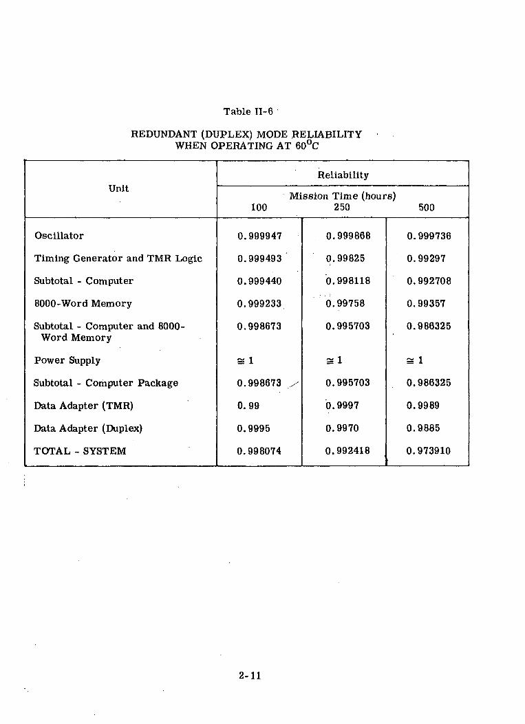
Table II-6
REDUNDANT (DUPLEX) MODE RELIABILITYWHEN OPERATING AT 60°C
Unit
Oscillator
Timing Generator and TMR Logic
Subtotal - Computer
8000-Word Memory
Subtotal - Computer and 8000-Word Memory
Power Supply
Subtotal - Computer Package
Data Adapter (TMR)
Data Adapter (Duplex)
TOTAL - SYSTEM
Reliability
Mission Time (hours)100 250 500
0.999947
0.999493
0.999440
0.999233
0.998673
S 1
0.998673 /
0.99
0.9995
0.998074
0.999868
0.99825
0.998118
0.99758
0.995703
£ 1
0.995703
0.9997
0.9970
0.992418
0.999736
0.99297
0.992708
0.99357
0.986325
S 1
0.986325
0.9989
0.9885
0.973910
2-11
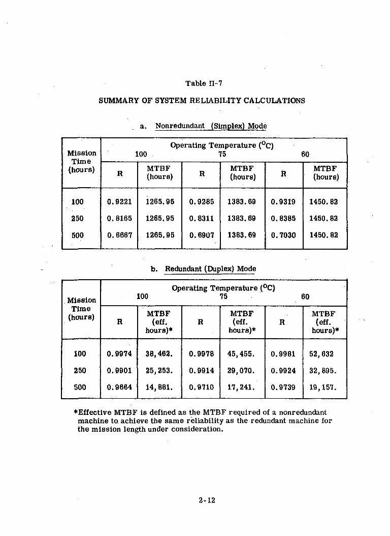
Table II-7
SUMMARY OF SYSTEM RELIABILITY CALCULATIONS
a. Nonredundant (Simplex) Mode
MissionTime
(hours)
loo
250
500
Operating Temperature (°C)100 75 60
R
0.9221
0.8165
0. 6667
MTBF(hours)
1265.95
1265.95
1265.95
R
0.9285
0.8311
0. 6907
MTBF(hours)
1383.69
1383.69
1383.69
R
0.9319
0.8385
0.7030
MTBF(hours)
1450. 82
1450. 82
1450. 82
b. Redundant (Duplex) Mode
MissionTime
(hours)
100
250
500
Operating Temperature (°C)100 75 60
R
0.9974
0.9901
0.9664
MTBF(eff.
hours)*
38,462.
25,253.
14,881.
R
0.9978
0.9914
0.9710
MTBF(eff.
hours)*
45,455.
29,070.
17,241.
R
0.9981
0.9924
0.9739
MTBF(eff.
hours)*
52, 632
32,895.
19,157.
*Effective MTBF is defined as the MTBF required of a nonredundantmachine to achieve the same reliability as the redundant machine forthe mission length under consideration.
2-12

Section in
SATURN V COMPUTER
3-1
Section in
SATURN V COMPUTER
A. GENERAL DESCRIPTION
The Saturn V computer is a serial machine using a random accessmagnetic core memory. It uses microminiature packaging techniques,developed under the Advanced Saturn Technology program; triple modularredundancy in the central computer; and multiple duplex memory modulesfor high reliability. Glass delay lines are used for the serial arithmeticregisters and for the storage of the instruction counter. The characteristicsof the computer are summarized in Table III-l.
The Saturn V computer provides general purpose computing capabilitycharacterized by high internal computing speed and variable capacity randomaccess core memory. The internal arithmetic structure employs both adderand multiplier units which may operate concurrently with a single programcontrol unit. This arrangement provides operating speeds up to 40 percentgreater than for a more conventional nonconcurrent arithmetic section atessentially no additional cost in components. To provide flexibility to theprogrammer and to conserve instruction words during the multiply process,an option is provided which permits or prohibits addition during multiplicationunder control of the programmer.
Memory words are 28 bits in length, (including two parity bits). Thememory is arranged so that one data word or two instructions may occupyone 28-bit memory word. The memory uses fourteen 64 by 128 (4,096 words)magnetic core planes plus the required drive and sensing circuits. From oneto eight memory modules may be used in the computer, providing flexibilityin memory size for different Saturn missions. Independent memory modulesmay be used in duplex fashion for high reliability on long missions. Thisreport assumes the use of 32,768 instruction words, or four modules. Thismemory space permits duplex operational capability, thus providing very highmemory reliability.
Reliability of the central computer is ensured by the use of triple mod-ular redundancy (TMR). The computer is divided into seven modules (definedin Table in-2), which are triplicated. Redundancy at this level provides re-liability superior to the duplex equipment approach and raises fewer designproblems than the use of quad components. Calculations and simulation showthat by using TMR central computer logic and duplex memory operation forthe mission phases, reliability of 0. 9957 for 250 hours for the computer logic,memory and power supply is achieved.
3-2

Table III-l
BATURN V COMPUTER CHARACTERISTICS
Type
Clock
Speed
Add Time, Accuracy
Multiply Time, Accuracy
Divide Time, Accuracy
Storage capacity (4 mem-ory modules)
Input/Output
Component count (in-cluding 4 memorymodules)
Temperature
Reliability
Stored program, general purpose, serialfixed point, binary
512 kilobits per second, 2.048 me clock
Add-subtract and multiply-dividesimultaneously:
82 usec, 26 bits
328 usec, 24 bits
656 usec, 24 bits
18,384 26-bit words plus two paritybits expandable in 4,096-wordmodules to 32,768 words total, thememory modules may be used in simplexor duplex operation. Memory can bedivided between program and data asdesired, typically:
2,000 data words (25 bits and sign)28,768 instructions (each 13 bits)
External - computer programmed I/Ocontrol
40,800 silicon semiconductors and cermetresistors; 458,752 ferrite cores
60°F inlet coolant temperature; 100°Cmaximum junction temperature allowable
0.996 probability of success for 250-hourmission using TMR logic and multipleduplex memory modules
3-3

Table III-1. Saturn V Computer Characteristics (cont)
Packaging
Weight
Volume
Power
78 electronic page assemblies, four 4,096-word (28 plane) memory assemblies.Integral liquid cooling.
80 pounds (dry weight) including four4,096-word memory assemblies
2.10 cubic feet
138 watts
Table HI-2
TMR COMPUTER MODULE BREAKDOWN
ModuleNumber
1
2
3
4
5
6
7
Pages perModule
1
2
1
3plus delay line
1
3
3
Module Name or Description
Computer Timing
Transfer Register
Arithmetic Unit
Multiply and Divide
Operation Code
Memory Address Register and De-coder
Memory Timing and Parity Check
3-4

The TMR system uses three identical simplex computer logic channelsand subdivides each channel into seven functional modules. The outputsfrom each channel are voted upon in voter circuits before the signal is sentto another module. The output of the voter circuit is equal to the majorityof the inputs to the circuit. Thus, even if one of the three inputs is in-correct, the output to the next module will be correct. Figure III-l is anexample of TMR voter signal outputs.
The voter circuits prevent the failure of one functional module fromcausing computer failure, because the computer modules are not dependentupon single modules for correct inputs.
Correct computations can be obtained, even with several malfunctionsin the computer, through the use of the modularized computer and moduleoutput voting providing two identical modules are not in error.
This method will provide greater reliability than using three independentcomputers. If the outputs from three independent computers were compared,any malfunction in two of the computers would cause the computation to be inerror.
An average of 13 output signals from each module are voted on. Thevoter circuit outputs may go to any of the other subdivided modules of thecomputer.
The Saturn V microminiature packaging permits the 40, 800 com-ponents in the machine to be packaged into an 80-pound unit occupying 2.10cubic feet.
3-5

A,M 3
DO
oA2M3-A3M3~
A,MC
V 1 *—»>
Ag M3 An M j
Ag MQ
A3M3 3^
A,M,A3M6
Figure IH-1. TMR Voter Signal Outputs
3-6

Electronic circuits are mounted on 0.3 in. square wafers on whichinter connection wiring and film resistors (cermet) have been deposited bysilk screen printing and subsequent firing operations. These are known asUnit Logic Devices (ULD). They are attached to Multilayer InterconnectionBoards (MIB) by solder reflow techniques. Each MIB has a capacity of 35ULD's.
Two MIB's are bonded back-to-back to a supporting metal frame. Thisassembly comprises a page. Pages are interconnected by back panel multi-layer printed circuit boards.
The central computer electronics units are packaged on 78 pages. Awelded compartmentized liquid cooled structure houses the computer elec-tronics units and delay line registers. Memory electronics units aremounted on MlB-type boards where possible. Each memory module is aself-contained unit with individual timing, control, drive, address, senseand inhibit circuitry.
TMR permits the subdivision of the computer into three simplex ma-chines for testing purposes. Significant machine register signals are broughtout to laboratory test equipment for troubleshooting during ground testing.The maintenance equipment will have the capability of observing registercontents by use of panel lights, and will also be able to control the voltageconnection of the voter circuits in each TMR module. This will permit usingtest programs to isolate malfunctions on a simplex level. Further mal-function Isolation will make use of module switching, test lights, and main-tenance probes.
Details of the computer design are discussed in the following sections,including aspects of logical organization, circuit design, maintainability,packaging design, and laboratory test equipment.
B. COMPUTER FUNCTIONAL DESCRIPTION
The computer information flow is illustrated in Figure IH-2. Thissimplified block diagram depicts the major data flow paths and associatedregister level logic. The timing logic and I/O section are not shown, butare described in this section under the Instruction Sequencing and ComputerI/O Capability portions.
1. CHARACTERISTICS
The computer is a serial, fixed point, stored program, general pur-pose machine which processes data using two's complement arithmetic.Two's complement arithmetic obviates the recomplementation cycle required
3-7

i =u2
t j-hLd
!
^^
v Ls.> J/./
\5c[
£•7f
r
t,
2
l|<
™
C
T e "
^v-\ ? <
°<g
ojjiJVT1_i_YI ^7f
B '
*i 1Ed:
1 ho ^
•f
iai1*-
_« ;
UJ
1J!I
I
i i :i
i5 <1*
m8I/>*}
i
COX
O-(<
a.
|O
^ Memory
Modules
u• i'
£o>sif,ot1LVC
O
**
aoOCounterg-ftoS
—|
83DUU
^— 'fc
3
to-§
2<
a!
.JCuS(/i|strsiac *~Li •;
11u _c
41V.i
. a••^ ^*ce
n
tVo~ E
•Si
o utot1151 •<
1
<f1 iX
U
.Q
1'3V
L
V
I
Mi1: 5nI—
a)
1a3<v11tT)ac.af1
CX"«O (OJ
QJ<tJ
— i
rUcJ63
i/i S
i/
1
H— *
x
«
(D
IP
_, S
2 o
.
O O
§?"5V
U.
o
u
0) >
s
Q
o
1.51
"-*.9-
o-1V"a
i *Co
E5i i jI iX•~ -a
u
3
>
f
2 o
r11
a>tofx ^
° §
u J
:Q
0
C
\
1 1
I1 Q
1
Tco .
-.1 1
5 o
0
5dS
i&•9Q1
^31
(J)
! S
•" Q
i>
> fl
,1 5
.3g
o
J.
^
fr I s
tj
—
o »_
9o jc
o Q
J1
ou -
g1
f ^
s—
L-'F
°
1 £
U
*
g
~1 '3
I
o
I?
OS
-3 1
1 S
J I
^
f^
io
cj
J<
2
d1,
j: >-
° <
?- ~
R
c^
uc
xo
w
^;
Cg
1J
^ll~
s^J
eg
| -„ s
JL
0|
allJ|oj <"»
O
.
| <
f •"•I"
'*
^
T
u o T
w)
•~: O
W
fj*
O
3-8

when using sign plus magnitude arithmetic. Special algorithms have been developedand implemented for multiplication and division of two's complement numbers.Multiplication is done four bits at a time and division two bits at a time.These algorithms are treated separately in the Arithmetic portion of thissection.
A random access magnetic core memory is used as the computer stor-age unit. A serial data rate of 512 kilobits per second is maintained by op-erating the memory units in a serial by byte, parallel by bit operating mode^This allows the memory to work with a serial arithmetic unit. The parallelread-write word length of 14 bits includes one parity bit to allow checking ofthe memory operations.
Storage external to the memory is located predominantly in the shiftregister area. High reliability in this area is achieved by using glass delaylines for arithmetic registers and counters. Delay lines are the best choicewhen the number of transistors which would be required for the variousregisters is considered.
2. ORGANIZATION
Each instruction is comprised of a four-bit operation code and a nine-bit operand address. The nine-bit address allows 512 locations to be directlyaddressed. The total memory is divided into sectors of 256 words, and con-tains a residual memory of 256 words. The nine-bit address specifies alocation in either the previously selected sector (data sector latches) or inthe residual memory. If the operand address bit (R) is a binary 0, then thedata will come from the sector specified by the sector register. If R is a 1the data comes from residual memory.
i.Instructions are addressed from an eight-bit instruction counter which
is augmented by a four-bit instruction sector register. Sector memory se-lection is changed by special instructions which change the contents of thesector register. Sector size is large enough so that this is not a frequentoperation.
Data words consist of 26 bits. Instruction words consist of 13 bits andare stored in memory two instructions per data word. Hence, instructionsare described as being stored in syllable one or syllable two of a memoryword. Two additional bits are used in the memory to provide parity checkingfor each of the two syllables. (Refer to Table m-3.)
3-9
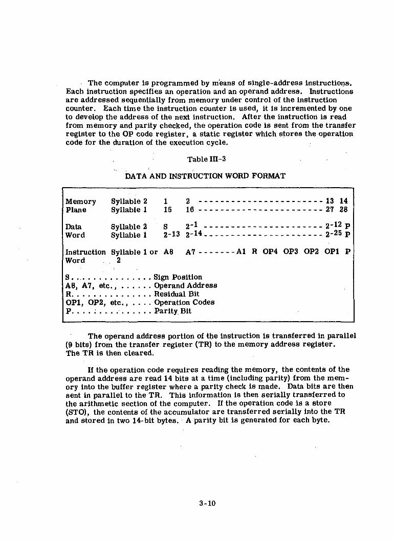
The computer is programmed by means of single-address instructions.Each instruction specifies an operation and an operand address. Instructionsare addressed sequentially from memory under control of the instructioncounter. Each time the instruction counter is used, it is incremented by oneto develop the address of the next instruction. After the instruction is readfrom memory and parity checked, the operation code is sent from the transferregister to the OP code register, a static register which stores the operationcode for the duration of the execution cycle.
Table IH-3
DATA AND INSTRUCTION WORD FORMAT
Memory Syllable 2 1 2 13 14Plane Syllable 1 15 16 27 28
Data Syllable 2 S 2'1 - 2~12 PWord Syllable 1 2-13 2-14 - 2-25 p
Instruction Syllable 1 or A8 A7 AIR OP4 OP3 OP2 OP1 PWord , 2
S . Sign PositionA8, A7, etc., Operand AddressR Residual BitOP1, OP2, etc., . . . . Operation CodesP. . . . ; . . . . Parity Bit
The operand address portion of the instruction is transferred in parallel(9 bits) from the transfer register (TR) to the memory address register.The TR is then cleared.
If the operation code requires reading the memory, the contents of theoperand address are read 14 bits at a time (including parity) from the mem-ory into the buffer register where a parity check is made. Data bits are thensent in parallel to the TR. This information is then serially transferred tothe arithmetic section of the computer. If the operation code is a store(STO), the contents of the accumulator are transferred serially into the TRand stored in two 14-bit bytes. A parity bit is generated for each byte.
3-10

Upon completion of the arithmetic operation, the contents of the in-struction counter are transferred serially into the TR. This information isthen transferred in parallel (just as the operand address had previously beentransferred) into the memory address register. The TR is then cleared andthe next instruction is read, thus completing one computer cycle.
The data word is read from the memory address specified by the mem-ory address register and from the sector specified by the sector register.Data from the memory goes directly to the arithmetic section of the computerwhere it is operated on as directed by the OP code.
The arithmetic section contains an add-subtract element, a multiply-divide element, and storage registers for the operands. Registers are re-quired for the accumulator, product, quotient, multiplicand, multiplier,positive remainder and negative remainder. The add-subtract and themultiply-divide elements operate independently of each other. Therefore,they can be programmed to operate concurrently if desired; i. e., the add-subtract element can do several short operations while the multiply-divideelement is in operation.
No dividend register is shown in FigureIII-2 because it is consideredto be the first remainder. The divisor is read from the accumulator duringthe first cycle time and can be regenerated from the two remainders on sub-sequent cycles. As indicated, both multiply and divide require more timefor execution than the rest of the computer operations. A special counter isused to keep track of the multiply-divide progress and stop the operation whencompleted. The product-quotient (PQ) register has been assigned an addressand is addressable from the operand address of any instruction. The answerwill remain in the PQ register until another multiply-divide is initiated.
3. TIMING
The three levels of computer timing are illustrated in Figure m-3.Basically, the computer is organized around a four clock system. The widthof each clock is approximately 0. 4 usec and the pulse repetition frequency is512 kilocycles. The bit time (four clock pulses) is 1.95 microseconds.Fourteen bit times occur in one phase time, resulting in a phase time of 27. 3microseconds. Three-phase times, PA, PB> and PC are required to per-form a complete computer operation cycle. Phase A (PA) makes up the in-struction cycle and phases B and C (PB and PC) make up the data cycle.
3-11

I I 2.048CLOCK TIME | Z | W | X | Y | Z | W | X | Y | Z | W | X— — — — — — 1 1 1 1 1 1 1 1 1 III
W CLOCK 1 ~| 1 1 I |
X CLOCK j | | |
Y CLOCK "1 | | | |
Z CLOCK | | | | | |
i i jl*~ 5WSEC H
nr
BIT TIME
I I
_10.512
jiSEC
27.3MSEC-
12 13 14
PHASE TIME
PA
PC
27.3/iSEC—«>|
A I B
1 1
1~l
111 1
FigureIII-3. Computer Timing
3-12
C. COMPUTER CONTROL
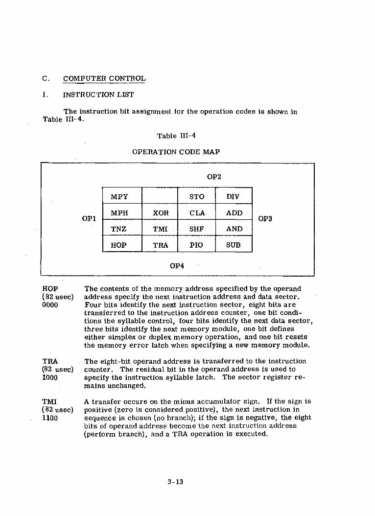
1. INSTRUCTION LIST
The instruction bit assignment for the operation codes is shown inTable III-4.
Table III-4
OPERATION CODE MAP
OP1
OP2
MPY
MPH
TNZ
HOP
XOR
TMI
TRA
STO
CLA
SHF
PIO
DIV
ADD
AND
SUB
OP4
OP3
HOP The contents of the memory address specified by the operand(82 usec) address specify the next instruction address and data sector.0000 Four bits identify the next instruction sector, eight bits are
transferred to the instruction address counter, one bit condi-tions the syllable control, four bits identify the next data sector,three bits identify the next memory module, one bit defineseither simplex or duplex memory operation, and one bit resetsthe memory error latch when specifying a new memory module.
TRA The eight-bit operand address is transferred to the instruction(82 usec) counter. The residual bit in the operand address is used to1000 specify the instruction syllable latch. The sector register re-
mains unchanged.
TMI A transfer occurs on the minus accumulator sign. If the sign is(82 usec) positive (zero is considered positive), the next instruction in1100 sequence is chosen (no branch); if the sign is negative, the eight
bits of operand address become the next instruction address(perform branch), and a TRA operation is executed.
3-13

TNZ(82 usec)0100
SHF(82 usec)1-110
AND(82 usec)0110
CLA(82 usec)1111
ADD(82 usec)0111
SUB(82 usec)0010
STO(82 usec)1011
DIV(656 usec)0011
MPY(328 usec)0001
A transfer occurs when the accumulator contains a nonzero num-ber. If the accumulator is zero, the next instruction in sequenceis chosen; if the accumulator is not zero (either negative orpositive), the eight bits of the operand address become the nextinstruction address, and a TRA operation is executed.
The SHF instruction shifts the accumulator contents right or leftone or two places as specified by the operand address.
Al Right Shift 1
A2 Right Shift 2
A5 Left Shift 1
A6 Left Shift 2
The contents of the memory location specified by the operandaddress are logically AND'ed, bit-by-bit, with the accumulatorcontents. The result is retained in the accumulator.
The contents of the location specified by the operand address aretransferred to the accumulator.
The contents of the location specified by the operand address areadded to the accumulator contents. The result is retained in theaccumulator.
The contents of the location specified by the operand address aresubtracted from the accumulator contents. The result is retainedin the accumulator.
The contents of the accumulator are stored in the location specifiedby the operand address. The contents of the accumulator are re-tained.
The contents of the accumulator are divided by the contents ofthe register specified by the operand address. The 24-bitquotient is in the product-quotient delay line. Concurrent useof the adder-subtracter element is required.
The contents of the memory location specified by the operandaddress are multiplied by the accumulator contents. The 24 high-order bits of the multiplier and multiplicand are multiplied to-gether to form a 24-bit product. Concurrent use of the add-subtract element is required. The product is stored in theproduct-quotient register.
3-14

MPH This is the multiply and hold operation. It is the same as the(410 usec) MPY operation except concurrent use of the add-subtract element0101 is not permitted and the product is stored in the accumulator.
XOR The contents of the memory location specified by the operand(82 usec) address are exclusively OR*d, bit-by-bit, with the contents of1101 the accumulator. The result is retained in the accumulator.
PIO The low order address bits, Al and A2, determine whether the(82 usec) operation is an input or output instruction. The high order1010 address bits, A8 and A9, determine whether the data contents
are transferred from the main memory, residual memory oraccumulator.
2. MULTIPLY AND DIVIDE TIMING
All operations except MPY, MPH and DIV require one operationalcycle (82 microseconds) for execution. The MPY and DIV instructions mustbe executed concurrently with any of the other instructions (except MPH).Three instructions can be executed between the start on the MPY and thetime when the product is available; similarly seven instructions can be ex-ecuted between the start and finish of DIV.
More one-word-time instructions can be inserted before the productor quotient is addressed if maximum efficiency is not required since multi-plication or division is stopped automatically and the result retained untiladdressed. Figure III-4 illustrates the timing of the MPY and DIV operations.
The MPH instruction inhibits further access to memory until completed,and cannot be operated concurrently with other operations.
3. INTERRUPT
A limited program interrupt feature is provided to aid the input/outputprocessing. An external signal can interrupt the computer program andcause a transfer to a subprogram. Interrupt occurs when the instruction inprogress is completed. The instruction counter, sector and module registers,and syllable latch are stored automatically in a reserved residual memorylocation (octal address 777). A HOP constant is retrieved from a secondreserved residual memory location (octal address 776). The HOP constantdesignates the start of the subprogram. Automatic storage of the accumulatorand product-quotient registers is not provided. This must be accomplishedby the subprogram. Protection against multiple interrupts and interruptsduring MPY and DIV operations is provided.
3-15

PHASETIMES
MPY
OlV
1
PA PB ^c
*T
4
82 f.
2
A B C
INST.
=1
4t
.SEC
3
A B
•1
•1
4
C
16
8
A B
20
10
PA
C
.-BI
ROODj
32
5
A
TS
24
12
B C
IN PAR
I"
J
)UCTjtESSABLE
SfiSEC
e
A B
T
C
TIAL PRO!
1"
A B C
UCT
B
A B C
9
A B C
^-BITS IN QUOTIENT
I8| 20 |22
QUOTADOR
69(
24
ENT•SSABLE
'MSEC
Figure III-4. MPY-DIV Timing Chart
The interrupt signal may be generated by a timed source. The rate atwhich it is generated is controlled by changing the magnitude of a numberwhich is being continually summed. When the summed number reaches apredetermined value, the interrupt signal is generated. This is accomplishedin the Saturn V Data Adapter (DA) equipment.
The main program can be resumed by addressing the contents of residualmemory word 777 with a HOP instruction.
Certain discrete input signals are allowed to cause interrupt. Theseare useful in causing the I/O subprogram to give immediate attention to aninput or output operation.
4. PROGRAMMING CONSIDERATIONS
The Saturn V Guidance Computer uses a conventional complement ofarithmetic instructions including add, subtract, multiply, and divide. Twomultiply instructions are included. MPY requires that one-word-time op-erations be performed in the adder unit during the multiplication processbecause the instruction counter advances each word-time. This procedurespeeds up the computer operation by permitting simultaneous multiplicationand one-word operations. Trial programming has shown a speed increaseof up to 40 percent over a conventional sequential computer.
3-16

When the program is multiply-limited, and a sufficient number of usefulone-word operations cannot be located in the portion of the flow diagram beingexecuted, the MPH instruction is used. This instruction inhibits advance ofthe instruction counter so no new instructions are read from memory untilthe operation is completed. This feature conserves program steps. Havingboth types of multiply instructions permits the increased speed of concurrentoperation without sacrifice in the number of program steps required, andpermits a programming tradeoff of speed and number of instructions required.
TRA, TMI, and TNZ instructions provide flexibility in programmingunconditional transfers; in branch instructions, through transfer of the con-tents of the accumulator; and in easy handling of discrete inputs, which areobtained in the accumulator through masking with an AND instruction.
The HOP instruction is used for transfers outside of the sector cur-rently being used. HOP permits jumping to another portion of the flow dia-gram and to subroutines. To return from a subroutine, the last instructionin the routine is a HOP. The HOP constant causes a return to the originalprogram sequence. Since each use of a subroutine in the program results inreturn to a different place in the flow diagram, the HOP constant is loadedprior to entering the subroutine. An automatic program compiler is used togenerate the correct HOP constants.
An exclusive OR operation, XOR, is provided to permit the rapidchecking of changes in discrete inputs, which are grouped into data-wordinputs. Discrete output words may be generated by masking out the bit tobe changed with an AND instruction and adding the discrete output into theselected position.
The product-quotient (P-Q) register can be addressed (by Octal 775)with the operations CLA, ADD, SUB, STO, AND and XOR.
The interrupt feature in the guidance computer facilitates the timingof input-output operations by causing a transfer to an input-output subprogram.The interrupt signal is generated in the DA and may be set to interrupt atthe highest rate at which any I/O quantity must be handled. This methodavoids the necessity of keeping track of time expired since last entering theI/O subprogram.
The automatic interrupt also makes it possible to permit certain dis-crete inputs to cause interrupt. Allowing discrete inputs to interrupt makesit possible to demand that the program give attention to an important dis-crete input. Communications between the guidance computer and the vehicletelemetry monitoring system are thus facilitated.
3-17

The vehicle monitor system is selected by an address code from thecomputer. The definition of which vehicle parameter is to be monitored isgiven over the outputlinesto the DA and stored in a buffer register. Whenthe monitor has acquired the desired parameter, an interrupt is generatedcausing the computer I/O subprogram to read the value of the parameter asan input. This scheme permits computing to continue while waiting for themonitor system to acquire the parameter.
The data sector register permits considerable flexibility in the handlingof data and constants. Instructions indicate whether data is located in theresidual sector or the sector referred to by the data sector register. Byconfining data to the residual register and a limited number of memorysectors, the changing of the data sector register can be minimized. Theresidual sector is then made more readily usable for data referred to byinstructions stored in many sectors. The small size of each sector, achievedby concentrating instructions rather than both data and instructions in eachsector, reduces the size of the instruction word and conserves memory coreplanes. The programmer is free to move between separate parts of the pro-gram without frequently changing instruction or data sector registers.
The data sector register is also useful in addressing sets of constantsstored for use with polynomial injection guidance equations. The instructionsnecessary to compute the polynomials are stored once. Sets of coefficientsfor the many different polynomials are each stored in different memorysectors. The coefficients can be readily retrieved by use of the data addressregister, which is set to select a given set of coefficients in the evaluationof the polynomial. Thus, the location of the polynomial number is set in thesector register and the coefficients are selected.
The separate instructions and data sector register feature eliminatesthe need for indexing, since it accomplishes the same end result in polynomialevaluation, the chief application of indexing. Hardware and instruction bitsare saved by omitting indexing.
Upper and lower limits for orbital checkout parameters are stored inthe two halves of a data word. Addressing of the parameter through themonitoring system is related to the storage location of the limits in memory.A simple, regular sequence of addresses makes programming easy by theuse of address modification techniques.
D. ARITHMETIC SECTION
1. GENERAL
The Saturn V Computer has two independent arithmetic elements, theadd-subtract element and the multiply-divide element. Although both operate
3-18

independently, they are serviced by the same program control circuits andmay be operated concurrently. During each program cycle-time, the add-subtract element can perform any one of the computer instructions, exceptMPY, MPH, and DIV. Also during each program cycle-time, the results ofthe simple arithmetic operations are circulated through the accumulatordelay line and through the accumulator sync delay line channel to preventprecessing of the results.
The multiply-divide element uses three channels of a delay line asshown in Figure III-3. One channel of the instruction counter delay line isused as a counter to stop the multiply or divide operations. Another channelof the instruction counter delay line is used to synchronize the product orquotient when the operation is completed. This is controlled automaticallyby the counter.
The product-quotient register is addressable as a residual memoryword and has the octal address 775. The product or quotient can be obtainedon any subsequent operation cycle after completion of the multiply or divideoperation, but must be used before initiation of another multiply or divideoperation. The product of the MPH operation is stored in the accumulator.
The recursion formulas for implementing multiply and divide instructionswith two's complement numbers are explained in the following paragraphs:
2. MULTIPLY
The multiply element operates in a two-phase cycle, serial-by-fourparallel, and requires 15 phase times, including instruction access time.The program initiates a multiply by placing the 24 high-order bits of thecontents of the memory location specified by the operand address into themultiplicand delay line. The multiplier delay line contains the 24 high-orderbits of the contents of the accumulator. The phase counter terminates amultiply instruction.
The instrumentation of the multiply algorithm requires three delay linechannels. Two of the channels contain the partial product and the multiplier.These channels shift both the partial product and the multiplier four placesto the right every two-phase cycle. The third channel contains the multipli-cand. The accumulator portion (fourth channel) of this delay line is not in-volved in the multiply operation and can be used concurrently with the multiplyoperation.
3-19

Upon initiation of a multiply and during every other phase time there-after, the five low-order bits of the multiplier (MRj, MR2, MR3, MR4, andMRs) are placed in latches or tratches and are used to condition addition orsubtraction of multiples of the multiplicand to the partial product.
]
The following algorithm is utilized for multiply:
Pi = 1/16 [P(i. D + A 1 + A 2 ]
Pj is the new partial product, and Al and A 2 are formed according to therules:
MR!
MR3
0
1
0
1
0
1
0
1
MR2
MR4
0
0
1
1
0
0
1
1
MRg
MR5
0
0
0
0
1
1
1
1
Al
0
+2M
+ 2M
+4M
-4M
-2M
-2M
0
A2
0
+8M
+ 8M
+ 16M
-16M
-8M
-8M
0
M represents the multiplicand. For the first multiplication cycleand MR} are made zeros.
3. DIVIDE
The divide element operates in a two-phase cycle, serial-by-two-parallel, and requires 27 phase times per divide, including instruction accesstime. The program initiates a divide by transferring the 26 bits of the ad-dressed memory location (divisor) and the 26 bits of the accumulator (dividend)to the divide element. The phase counter terminates a divide operation.
3-20

The following algorithm is instrumented to execute divide:
Qi = «ie ' DVs + RTs • DVs" (1)
and
Ri+1 = 2Ri + (1 - 2Qi) DV (2)
where:
i = 1, 2, 3, . . .24
Qj - The ith quotient bit
RiS = The sign of the itn remainder
DVS = The sign of the divisor
Rj = The itn remainder
Rj = The dividend
DV = The divisor
Equation (1) states that the i^ quotient bit is equal to a "1" if the sign of theith remainder is identical to the sign of the divisor. The high-order quotientbit (sign bit) is the only exception to this rule. Qj as determined by equation(1) is used to solve equation (2) but must be complemented before it is storedas the sign bit of the quotient.
The instrumentation of the divide algorithm requires three channels of adelay line. One channel contains the quotient; one the divisor; and one the divi-dend. These three channels are used during multiply to contain the multiplier,the multiplicand, and the partial product respectively. The quotient and theremainder channels of the delay line have been lengthened by latches to shifttwo places to the left each two-phase cycle. The divisor circulates once eachtwo-phase cycle.
In the two's complement number system, the high-order bit determinesthe sign of the number. Since this is the last bit read from memory, it is im-possible to solve Equations (1) or (2) until the entire divisor has been readfrom memory. However, Equations (1) and (2) can have only two possible so-lutions.
Either,
Qi = 1
3-21

and,
R(i+l) = 2Ri - DV
or,
Qi = 0
and,
) = 2Rt + DV
Both the borrow of 2Ri - DV and the carry of 2Ri + DV are generatedas the dividend and divisor registers are loaded. When the sign bits of thesequantities are finally entered into their respective registers, Equation (1) issolved for the first quotient bit. K this quotient bit is a one, the borrow isexamined to determine the second quotient bit. If the first quotient bit is azero, the carry is examined to determine the second quotient bit. The fol-lowing truth table is solved to determine the second quotient bit if the firstquotient bit is a one.
Hi DVS B R(1+1)g Q
0 0 0 0 10 0 1 1 00 1 0 1 10 1 1 0 01 0 0 1 01 0 1 0 11 1 0 0 01 1 1 1 1
Where
R! = The first remainder bit to the right of the sign bit
DVS = The divisor sign
B = The borrow into the RI, DVS position
R(i+l) = Tne siSn °* tne new remainder
Q = The quotient bit as determined by comparing DVS
with R(i+l)s according to Equation (2).
3-22

Q = RI DVS- B + RI DVS B + RI- DVS- B + Rf DV8- B
= R~i- B (DVS + DVS) + Rt- B (DVS + DVS)
The equation used in generating the new remainder, Ri+2> is obtainedby expanding Equation (2)
i)) DV
R(i+2) = 2[2Ri + (1 - 2Qi) DVJ + (1 - 2Q(i+1)) DV
R(i+2) = 4R4 + 2 (1 - 2Qi) DV + (1 - 2Q1+i) DV
As R(i+2) is being generated, the next iteration of divide is started bygenerating, as already described, the borrow and carry for 2Ri+2 * DV-
E. MEMORY
The memory for the Saturn V Guidance Computer uses conventionaltoroidal cores in a unique self -correcting duplex system for achieving amemory reliability of 0.9976 for 250 hours of duplex operation or 0.958 for250 hours when operating simplex (for 8000 words of memory). The mem-ory consists of four identical 4096-word memory modules which may beoperated in simplex for increased storage capability or in duplex pairs forhigh reliability. The basic computer program is loaded at electronic speedsinto the instruction and constants sectors of the memory on the ground justprior to launch. Thereafter, the information content of constants and datacan be electrically altered, but only under control of the computer program.
The self- correcting duplex system uses an odd-even parity bit detectionscheme in conjunction with memory drive current error detection circuitryfor malfunction indication and correction. Unlike conventional toroid randomaccess memories, the self- correcting extension of the basic duplex approachpermits regeneration of correct information after transients or intermittentfailures which otherwise would result in destructive read- out of the memory.
3-23
F. BASIC MEMORY SYSTEM OPERATION
Figure in-5 is a simplified block diagram of the computer memory sys-tem. The configuration consists of a pair of memories providing storage for8192 14-bit memory words when operating duplex, or 16,384 14-bit memorywords when simplex operation is desired. Each of the simplex memories in-cludes independent peripheral instrumentation consisting of timing, control,address drivers, inhibit drivers, sense amplifiers, error detection circuitryand I/O connections to facilitate failure isolation. Computer functions com-mon to these simplex units consist of the following:
• Memory address register outputs
• Memory transfer register .input-output
• Store gate command
• Read gate command
• Syllable control gates
Computer functions, which are separate for each simplex memory,consist of the synchronizing gates, which provide conversion of the serialdata rate of 512 kilobits per second required by the computer to generate astart memory unit command at 128 kilobits per second. These gates also
provide selection of multiple simplex memory units for storage flexibility andpermit partial or total duplex operation throughout the mission profile forpurposes of extending the mean-time-before-failure for long mission times.Each of the simplex units can operate independently of the others or in a .rduplex manner.
Memory modules are divided into two groups, one group consisting ofeven numbered moduled (0-6), the other consisting of odd numbered modules(1-7). A buffer register associated with each group is set by the selectedmodules. >
3-24

For duplex operation, as shown in Figure III-5, each memory is undercontrol of independent buffer registers when both memories are operatingwithout failure. Both memories are simultaneously read and updated inparallel (14 bits). A single cycle is required for reading instructions (13bits plus 1 parity bit per instruction word). Two memory cycles are re-quired for reading and updating data (26 bits plus 2 parity bits).
The parallel outputs of the memory buffer registers are serialized at a512-kilobit rate at the memory transfer register under control of the mem-ory select logic. Initially, the outputs of only one buffer register are beingused with simultaneous parallel parity checking being performed on bothregister outputs. When an error is detected in the memory being used, op-eration immediately transfers to the other memory. Both memories arethen regenerated by the buffer register of the "good" memory, thus cor-recting transient errors.
After the parity-checking and error detection circuits have verified thatthe erroneous memory has been corrected, operation returns to the conditionwhere each memory is under control of it's own buffer register. Operation isnot transferred to the previously erroneous memory until the "good" memorydevelops its first error. Consequently, instantaneous switching from onememory output to another permits uninterrupted computer operation untilsimultaneous failures at the same location in both memories cause completesystem failure.
Proper operation of the memory system during read cycles is indi-cated by each 14-bit word containing an odd number of "one's" and a logical"one" output of the error detecting circuitry. If either or both of theseconditions are violated, operation is transferred to the other memory.
During regenerate or store cycles parity checking cannot be performed.Failure detection is accomplished by the error detection circuitry only.Parity checking is performed during subsequent read cycles.
3-25
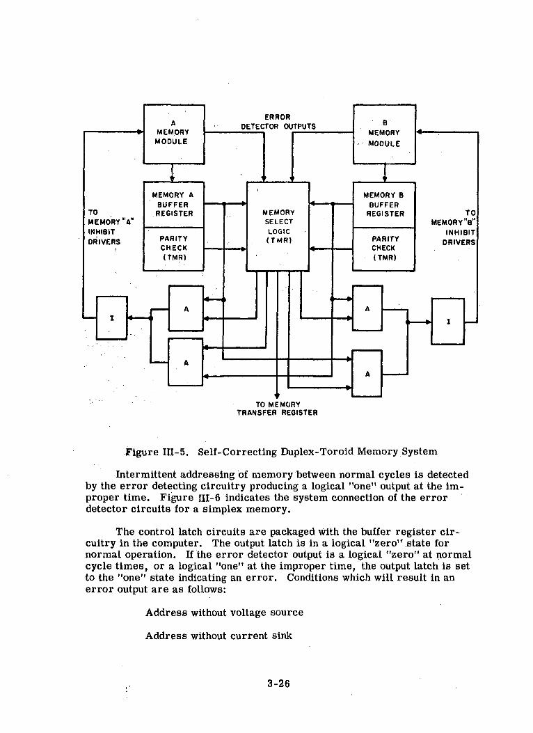
TOMEMORYV
INHIBITDRIVERS
ERRORDETECTOR OUTPUTS
MEMORY BBUFFER
REGISTERMEMORYSELECTLOGIC(TMR)
TO MEMORYTRANSFER REGISTER
Figure III-5. Self-Correcting Duplex-Tor old Memory System
Intermittent addressing of memory between normal cycles is detectedby the error detecting circuitry producing a logical "one" output at the im-proper time. Figure III-6 indicates the system connection of the errordetector circuits for a simplex memory.
The control latch circuits are packaged with the buffer register cir-cuitry in the computer. The output latch is in a logical "zero".state fornormal operation. If the error detector output is a logical "zero" at normalcycle times, or a logical "one" at the improper time, the output latch is setto the "one" state indicating an error. Conditions which will result in anerror output are as follows:
Address without voltage source
Address without current sink
3-26

No address
Dual source-single sink address
Single source-dual sink address
24
1
LINES to CRX •TCV
XV —
1
E l
—
^
L
RESET * LERROR PULSETO MEMORYSELECT LOGICAND DA
16 LINES 16-Y CURRENT SINKS •TCV
LEGENDCRXAND CRY s CURRENT REGULATOR
TCV = TEMPERATURE CONTROLLED VOLTAGEED'ERROR DETECTOR(2 PER MEMORY MODULE)
Figure III-6. X-Y Coordinate Half-Select Current Error Detection
G. COMPUTER INPUT/OUTPUT CAPABILITY
1. GENERAL
The computer input/output capabilities are characterized by the input/output instruction and the interrupt feature. The Process Input/Output (PIO)instruction provides for transferring of a single word into or out of theaccumulator or out of the memory.
3-27

The primary input/output interface will be between the computer andthe DA. The DA will perform all conversion (analog-to-digital and digital-to-analog) required by the system.
2. PIO INSTRUCTION
The PIO instruction transfers data between the accumulator or memoryand one-word registers and delay lines located in the DA or other subsystem.The operand address is used to select the desired register.
Discrete inputs and outputs can be processed by this instruction. It ispossible to pack 26 discrete signals into one word. The XOR instruction willdetermine if any of the 26 discrete inputs has changed state. The AND in-struction is used to set or reset any of the discrete outputs.
3. INTERRUPT
Interrupt signals can be generated within the DA. These signals willstop the computer program and cause a branch to a subprogram. The locationof the subprogram is program-controlled and is dependent upon the HOP con-stant stored in a specific memory location. This subprogram will normallybe used to process a block of input-output data on a periodic basis. The rateat which the timed interrupt occurs is also program-controlled and can beadjusted as dictated by the various modes of operation during a given mission.
The main program can be resumed after completion of the subprogramby executing a HOP operation from another specified memory location. Thislocation will contain the contents of the instruction counter,, sector register,and syllable latch, which were stored there when the interrupt occurred.
H. LOGIC CIRCUITS
1. DESIGN
Many different logic circuit techniques were evaluated before the finalcircuit configuration was chosen. The circuit configuration, a form of cur-rent switching diode logic, was found to have these advantages (listed in orderof importance):
• Reliability: The circuits are inherently simple and are capableof yielding large component drift allowances in a large per-centage of logical applications.
• Low Power; The circuit is designed to minimize power bysacrificing only the very high speeds. Also, many of the ANDresistors are clocked and, hence, need power only when theyare interrogated.
3-28
• Speed: Signal voltage levels are kept as low as possible to achieverelatively high speeds without sacrificing power.
Most of the computer circuits use ultra-high-speed silicon planarepitaxial transistors and dual silicon planar diodes.
Simultaneous worst-case design was used for all of the circuits. Thistakes into account supply voltages, input responses and levels, environmentalconditions, and component drift with life. The end-of-life component con-ditions are determined from environmental and operating life testing. Cir-cuits are designed, where applicable, such that input signal noise, powersupply noise, and output signal noise, may all occur simultaneously withoutcausing circuit failure.
Release of a circuit for production was made only after laboratoryevaluation verified circuit performance of a circuit breadboard consistingof selected worst-case components.
The number of different circuit types utilized has been minimized. Onestandard inverter circuit serves the logical inversion function and, in con-Junction with standard AND-OR diode logic circuits, is instrumented to serveas a latch, the equivalent of a flip-flop. Buffer storage circuits of the latchtype have the advantages of being d-c coupled, and relatively insensitive tonoise. In addition, these circuit types do not require critical input signalresponse times.
2. BASIC LOGIC CIRCUITS
The basic logic circuits consist of an AND-OR-INVERT circuit familywhich uses diode logic and a transistor, operated in the saturated and cut-offmodes. The logic circuits are designed to operate at 512 kilocycles in afour clock-per-bit system. The Computer clocks synchronously gate logicsignals by applying a six volt pulse to the AND resistors. Clocking the ANDresistor, together with proper selection of the clock down level, allows in-creased capability of the inverter through time-sharing of loads and alsoeliminates the need for an AND diode for each clocked AND.
The logic ground rules provide that an AND may have up to ten logicinputs in addition to a clock; an OR may have up to four inputs. Since theinverter load is phased with respect to the inverter drive, there are twovalues available for the AND resistor. When the inverter is driven by a2. 5k AND, it may drive five 2. 5k ANDS or three 1. 5k ANDS. When theinverter is driven by a 1. 5k AND, it may drive 16 2. 5k ANDS of ten1. 5K ANDS. The AND loads may be a mixture of two AND resistor valueswhere a 2. 5K AND is equivalent to three-fifths of a 1. 5K AND in terms of
3-29

loading. The availability of two AND resistor values has the net effect ofallowing one inverter to perform functions which would normally require twoinverters. The inverter AND loads, in addition to being phased with respectto the drive, may occur at different clock times and may then be time-shared.This results because an AND with its clock input in the down state presents noloading on an inverter. The principle of time-sharing may also be used toextend the number of allowable OR inputs. Also, a 2. 5k AND is equivalent tohalf a 1. 5k AND in terms of OR fan-in. Thus, the OR fan-in may be as highas eight at any one clock time.
The layout of the logic circuits was limited by basic design needs. Thechoice of a 0. 3 inch ULD substrate dictated that only 12 of the available ULDconnections could be used. The number of different types of ULD's has beenminimized and all logical connective functions are satisfied with a minimumof ULD's.
Examples of the two highest usage blocks are shown in Figures III-7and III-8. Figure III-7 shows an INV module which contains an inverterwith a permanently connected 1. 5k AND and an extra 2. 5k AND. Two INVmodules are required to form a latch. The AA module of Figure HI-8 isused to obtain AND and OR diodes and AND resistors. For example, the AAmodule may be used to obtain two three-input 2. 5k AND's with two OR diodes,a seven-input 2. 5k AND with one OR diode, or just to obtain eight AND diodes.The versatility of these modules allows just two modules to satisfy all logicconnections with minimum waste of unused components.
I. SPECIAL CIRCUITS
1. GENERAL
In addition to the basic logic circuits, several other special circuits arerequired by the computer. These circuits are associated with delay lines,timing generation, memory, and input and output functions. They arereferred to as special since they are designed for a unique function, andusually have only limited usage.
2. VOTER CIRCUIT
A voter circuit is required to instrument triple modular redundancy.The following requirements are imposed on the voter circuit by TMR:
• The voter output must represent the majority of three inputs.
• The voter reliability must be as high as possible because of theinfluence of voter reliability on overall computer reliability.
3-30

7o
TOP VIEW 10X
CR1
3o
4o
'1.5K
CR2
CR3 CR4
'1.8K
O6
;R37.8K
O2
R22.5K!
CR5 CR6
10
BOTTOM VIEW 10X(REVERSED)
1 REST. PASTE
Figure III-7.. INV Module
3-31
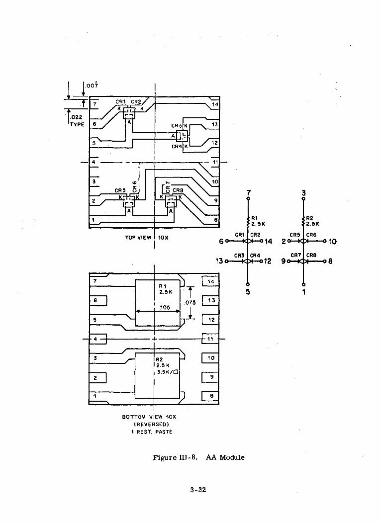
CR3
f
7
T35 ^
\THJLJ
s~3 y-
ZD
1
">
D 1
2.5K
J
R22.5K
3 R V //~|
\
t.073
II
71-
\J
I
n: —14
CE^L
rrrL1L
.if.9
8
3o
CR4
CR5
CRT
i i
5
JR22.OK
CR6
CR890-HOI——08
1 11
BOTTOM VIEW 10X(REVERSED)
1 REST. PASTE
Figure III-8. AA Module
3-32

• The signal delay through the voter circuit must be small enoughso that the complexity of the nonredundant module is not increasedwhen the voter is added.
• The voting circuit requires a juncture of the three module outputs.This juncture must be so constructed that a failure of one modulecannot possibly affect either of the other two modules. Also, thefailure of a voter component must not cause failure of a moduleand thus cause failure of other outputs of that module.
• The voter circuit must be capable of operating in simplex mode,in the interest of computer checkout.
The voter circuit consists of a current summing network which issensed by an inverter. The output of the inverter is then amplified with anadditional inverter to supply an output capable of driving ten 1. 5k AND's.A power voter is also available which amplifies the inverter output to a capa-bility of twenty 1. 5k AND's. The delay through the voter circuits is less thanone clock time by the amount of allowable skew between clocks of the threeclock channels.
3. DISAGREEMENT DETECTOR
Disagreement detectors provide an output if any of the triplicatedmodules faiL The disagreement detector consists of a three-way exclusiveOR, which is connected to each set of outputs of each trio of modules. Thereare approximately two-hundred disagreement detectors in the Saturn VGuidance Computer. The outputs of several disagreement detectors areOR'd together to provide fewer outputs to the DA where a register storesdisagreement detector outputs for transmission over telemetry. The inputsto the disagreement detectors are clocked to allow time for the inputs to reachsteady state conditions before sampling.
4. DELAY LINE CIRCUITS
Ultrasonic delay lines are utilized for short term storage. The delaymedium is zero temperature-coefficient glass. One bit of information is a0.2 microsecond pulse which propagates through the delay medium at thespeed of sound in the medium. Ceramic transducers are used for energyconversion. Glass delay lines provide very reliable and stable short-termstorage along with simple instrumentation.
The maximum data rate of the delay line in this computer is 2 mega-cycles. Thus, only one delay line, delay line driver, and sense amplifiercombination are required for storage of up to four different logic channels.This time-sharing of the delay line, plus driver and sense amplifier, iseasily implemented by gating the driver input and sense amplifier output withthe four computer clocks.
3-33
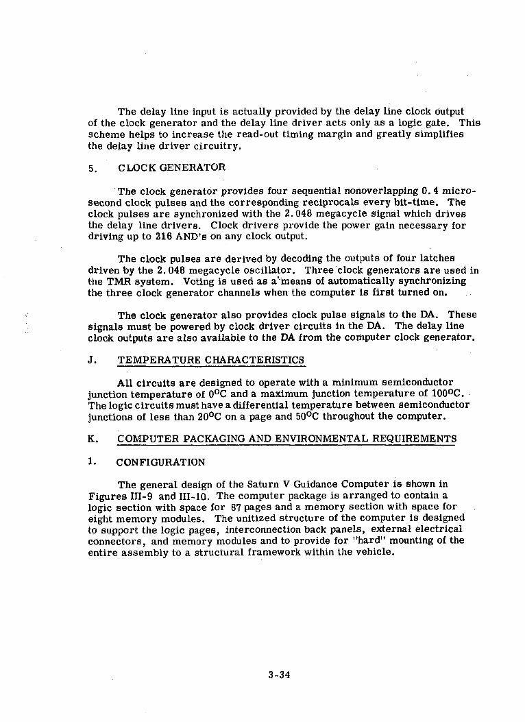
The delay line input is actually provided by the delay line clock outputof the clock generator and the delay line driver acts only as a logic gate. Thisscheme helps to increase the read-out timing margin and greatly simplifiesthe delay line driver circuitry.
5. CLOCK GENERATOR
The clock generator provides four sequential nonoverlapping 0. 4 micro-second clock pulses and the corresponding reciprocals every bit-time. Theclock pulses are synchronized with the 2.048 megacycle signal which drivesthe delay line drivers. Clock drivers provide the power gain necessary fordriving up to 216 AND's on any clock output.
The clock pulses are derived by decoding the outputs of four latchesdriven by the 2.048 megacycle oscillator. Three clock generators are used inthe TMR system. Voting is used as a'means of automatically synchronizingthe three clock generator channels when the computer is first turned on.
The clock generator also provides clock pulse signals to the DA. Thesesignals must be powered by clock driver circuits in the DA. The delay lineclock outputs are also available to the DA from the computer clock generator.
J. TEMPERATURE CHARACTERISTICS
All circuits are designed to operate with a minimum semiconductorjunction temperature of 0°C and a maximum junction temperature of 100°C.The logic circuits must have a differential temperature between semiconductorjunctions of less than 20°C on a page and 50°C throughout the computer.
K. COMPUTER PACKAGING AND ENVIRONMENTAL REQUIREMENTS
1. CONFIGURATION
The general design of the Saturn V Guidance Computer is shown inFigures III-9 and III-10. The computer package is arranged to contain alogic section with space for 87 pages and a memory section with space foreight memory modules. The unitized structure of the computer is designedto support the logic pages, interconnection back panels, external electricalconnectors, and memory modules and to provide for "hard" mounting of theentire assembly to a structural framework within the vehicle.
3-34

89 T
( j
LOGIC MEMORY
-T
CONNECTOR
PAGE
3 SPARE
• INTERCONNECTION
CHANNEL
12
3
4
5
SPARES
TOTAL
Figure III-9. Memory and Logic Assembly
3-35
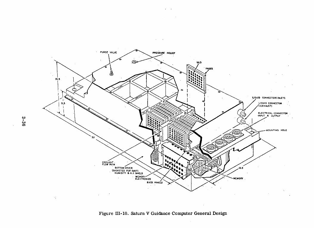
.1in&•at-i0)0)ao(Uoc>g5a0)
3-36
Logic pages and memory modules can be easily removed and replacedafter removal of the protective covers. The external electrical connectorsare located on the framework to allow for the convenient connecting or dis-connecting of mating connectors and to minimize possible interference withadjacent units. Heat generated by the logic pages and memory modules isabsorbed by cooling fluid circulating through passages in the structural wallsof the computer package.
2. MATERIAL
Light-weight magnesium-lithium alloy is used to fabricate the structuralgridwork. The structure is designed to a safety factor equal to or less than1.5. Material used in the fluid passages is compatible with a water-menthanol cooling solution in order to enhance heat transfer effectivenessand to resist corrosion.
3. SEALING DESIGN
The sealing design of the computer provides RF shielding and dustexclusion. In addition, the computer is sealed to the extent that 1 psig willleak off to atmospheric or ambient pressure within a 2-minute minimum per-iod when the unit is pressurized to 5 psig.
4. SIZE AND WEIGHT
The dimensions of the computer are approximately 30 inches long, 12inches wide and 10. 5 inches high. The mounting bosses are positioned so 'that 5 inches of the vertical dimension of the computer are located on oneside of the plane defined by the mounting surfaces, and 5. 5 inches on theother side.
A computer with four memory modules and 78 logic pages will weighapproximately 80 pounds and occupy a volume of approximately 2.10 cubicfeet. The estimated weights of the computer sections are as follows:
Logic Weight (Ibs)
Pages (occupying 78 page spaces) 11.1
Connectors 13.4
Supporting Structure 22.6
Wiring 3.6
3-37

Memory Weight (Ibs)
Assembly and Mounting Structure 22.0(
Electronics 3.3
Growth Factor 6.5
These weight estimates exclude the weight of the cooling fluid.
5. COOLING
Those electronic items which dictate the overall thermal design of theSaturn V Computer are as follows:
• Allowable ULD transistor junction temperature... 100°C.
• Allowable temperature differential per machine page... 20°C.
• Allowable temperature differential within any one machine... 50°C.
• Allowable temperature level of memory array... 70°C.
• Allowable temperature differential over entire array... 10°C.
An integral cooling system is incorporated within the computer design.The operating specifications for the coolant are as follows:
• Maximum input coolant temperature = 60°F
• Maximum allowable flow rate = 12 Ib/min.
• Maximum allowable pressure drop(including one main liquid disconnect) = 3.5 psi
The coolant is channelled through the frame as shown in Figure III-10.In addition, the liquid channels are drilled or cast into the magnesium-lithium structure in order to obtain satisfactory distribution of the liquidand the highest possible heat transfer coefficient.
The transfer path for the heat generated by the ULD's is:
• From the ULD to the MIB board and metallic page structure,then
3-38

• From the page structure to the metallic clip attached on the pageextremities, and finally
• From the clip to the fluid passing through the machine framestructure.
Heat transfer coefficients in the range of 50-70 BTU/Hr. - Ft2 - F°are obtained in the vicinity of the clip mounting structure. A temperaturedifferential of 2 degrees Fahrenheit/watt of page dissipation exists at eachclip interface. Summing all the temperature differentials, the maximumexpected transistor junction temperature is 140°F (80°C).
L. ENVIRONMENTAL REQUIREMENTS
The Saturn V Computer is designed to operate without malfunction whensubjected to the following environmental conditions:
• The computer will be operated for 1 hour at 200,000 ft altitudefollowed by 4 hours of operation at 100°F chamber radiationwall temperature. The emissivity of the radiation chamber wallwill not be less than 0.8.
• The chamber wall temperature will then be reduced to minus 40°Fin a period not to exceed 1 hour and the computer will be oper-ated for 4 hours.
• The computer will be placed in a vacuum chamber and thepressure reduced to 10-4mm Hg (Torrs). The chamber walltemperature will be stabilized at 80°F and the computer willbe operated for not less than 500 hours after temperaturestabilization within the computer.
• The computer will be subjected to humidity and explosive at-mosphere in accordance with paragraph 4.41 of MIL-E-5272Cand paragraph 4.13.4 of MIL-E-5272C.
• The computer will be operated at 15g sustained acceleration inthe horizontal plane normal to the 30-inch mounting dimension fora minimum of 6 minutes.
• The computer will be subjected to three 50g shock saw-toothwaves having a 6 millisecond rise time and a 0. 5 milliseconddecay time. This shock will be imposed in the horizontal planenormal to the 30-inch mountingdimension of the computer.
3-39

• The computer will be subjected to a 140 db over-all acoustic noiselevel in a bandwidth of 37. 5 cps to 10 kc.
• The computer will be subjected to an acceptance test vibrationlevel of 3G RMS sine in the three principal axes at a sweep rateof 1 octave/min in the direction of increasing frequency only.
• The computer will be subjected to a qualification test of 0.057g2/cps random noise in a 40 to 1800 cps band with a 6 db peroctave roll off below 40 cps. Above 1800 cps, the roll-off is 12db/octave. This energy will be applied for 3 minutes after whichthe general spectrum will be reduced to 0.032 g2/cps. Thisenergy will be applied for 7 minutes. This test will be applied tothe computer in the three principal axes.
• The computer will be designed for fuel compatibility for an ex-posure time consistent with mission requirements.
The thermal operating design requirements will be met by the fol-lowing coolant requirements:
Fluid: 60 percent by weight methanol and 40 percentby weight water solution
Quantity: 12 Ib/min
Pressure Drop: A Pmax = 3.5 psi
Inlet Temperature: 50°F to 60<>F
The vibration requirements will be met by hard mounting the com-puter to channels within the missile.
M. ELECTRONIC PACKAGING
1. UNIT LOGIC DEVICE (ULD)
The basic circuit module is a ceramic substrate with deposited re-sistors and uncased semiconductor devices. The alumina substrate is 0.300inch square. Resistors are formed on the surface of the substrate bysilk-screen deposition of cermet resistor materials. Metallic conductorsare also formed by the same process. Transistors and diodes are attachedby reflow of solder-coatings previously applied to conductor surfaces. Anencapsulation material is applied to protect the components.
3-40

Connections with external circuitry and between opposite surfaces ofthe substrate are made through 14 wrap-around conductor lands and metalclips on the edges of the substrate. Figure IH-1.1 shows a ULD before andafter encapsulation.
2. MULTILAYER INTERCONNECTION BOARD (MIB)
Interconnections among ULD's are accomplished by the MultilayerInterconnection Board. The MIB is composed of multiple layers of etchedcircuits which are bonded together under heat and pressure to form a singleunit. Connections between circuit layers and to the outer surfaces areprovided by plated-through holes. Circuit layers are arranged for optimumcircuit isolation.
Each MIB contains 12 layers of copper assigned as shown in Figure111-12. Several layer patterns are shown in Figures 111-13, 111-14 and III-15'.All plated holes and conductors are located on a 0.020 inch grid. Conductorsare nominally 0.010 inch wide. Nominal separation of adjacent conductorsis 0.010 inch. The MIB has mounting area for 35 ULD's on 0.400 inch cen-ters. Figure III-16 shows front and rear views of a MIB before trimming.
3. PAGE
ULD's and MIB's in the computer logic are combined in page form.The page includes two MIB's bonded to both faces of a magnesium-lithiumalloy frame. A 98-pin connector is fastened to the lower edge of the frameand wire leads from the connector are soldered in plated holes on the edgeof both MIB's. Feed-through connections between the two MIB's are providedby insulated pins fastened in holes in the frame. Pin ends are soldered inplated holes of both MIB's. Test point lands are provided along the upperedge of each MIB.
Mechanical support for the page is provided on the lower end by theconnector shell and guide pins and on the upper end by clamping two lugs onthe page frame to the computer structure. Spring clips which grip both sidesof the page provide additional mechanical support and provide the principalthermal path from the page to the computer structure.
Electrical and mechanical attachment of ULD's to MIB's is by solderfillet connections. Both MIB and ULD land surfaces are pre-coated withsolder. The solder is re-flowed by infra-red heating to form solder fillets.After page assembly and test, a. coating is applied for protection in a highhumidity environment. A page mockup is shown in Figure III-17.
3-41

831
awJ-.cu0)(H0>
PQ3PS0)
3-4
2

///////////
0.004 ADHESIVE
COPPER 1 OZ.
V / /\ 0.004 LAMINATE MICAPLY
ULO PATTERN
OR EXTENDEROR EXTENDER
-3V SUPPLY
COLLECTOR OR AND EXTENDER
COLLECTOR OR AND EXTENDER
GROUND
AND EXTENDER OR COLLECTOR
AND EXTENDER OR COLLECTOR
+ 6V SUPPLYCLOCKS
CLOCKS
Figure III-12. MIB Cross Section
4. BACK PANEL
Interconnections among pages of the logic section are made throughback panels. The back panel consists of a MLB, receptacles for pages and ametal plate for mechanical support. The MIB is bonded to the plate and theleads of the receptacle are soldered to plated holes in the MIB.
5. MEMORY
The toroid memory module contains 14 core planes stacked betweenmechanical supports. Each plane has 8192 toroids 64 by 128 in a frame ap-proximately 5. 5 inches long by 3. 5 inches wide by 0.150 inches thick. Inter-connections between planes are made with printed wiring strips, soldered tothe plane edge terminals.
The mechanical supports on each end contain diode matrices andtermination resistors. These supports also provide mounting surfaces onfour sides for MIB's, mounting surfaces across one end for a discrete com-ponent connector and panel, and pads for mounting the memory module intothe computer frame.
3-43

Figure HI-13. MTO Top Land Pattern
The four MIB's mounted to the end supports contain memory circuitULD's. The discrete components panel has a 98-pin input-output connectorfor interconnections between the memory module and the computer logic.Flat cable wiring is used to make electrical connections between MIB's andthe core planes within the array.
The memory module volume is approximately 110 cubic in. and theweight 6.43 pounds. Memory configuration is shown in Figure III-18.
6. INTERCONNECTIONS
The logic pages are grouped in five channels in the computer. Thesechannels contain space for 16 to 20 pages. Interconnections within eachchannel are provided by a back panel. Connections among channels arethrough etched flexible flat cables. Adjacent areas on the five back panelsare interconnected by cables made in a few basic sizes and connected toconventional 98-pin page connectors. Figure 111-19 shows the flat cableartwork.
3-44

Figure 111-14. Mm Circuit Layer
Connections from back panels to external connectors are made througha harness which is attached at one end to terminal blocks on the back panelsand at the other end to the connector pins.
Memory modules are connected to the computer through flat cableswhich are permanently fastened to the computer back panels at one end andhave a pluggable connection to the memory module on the other end.
A diagram of computer interconnection wiring is shown in Figure III-2011-21 shows the physical arrangement of elements of the interconnection
system.
3-45
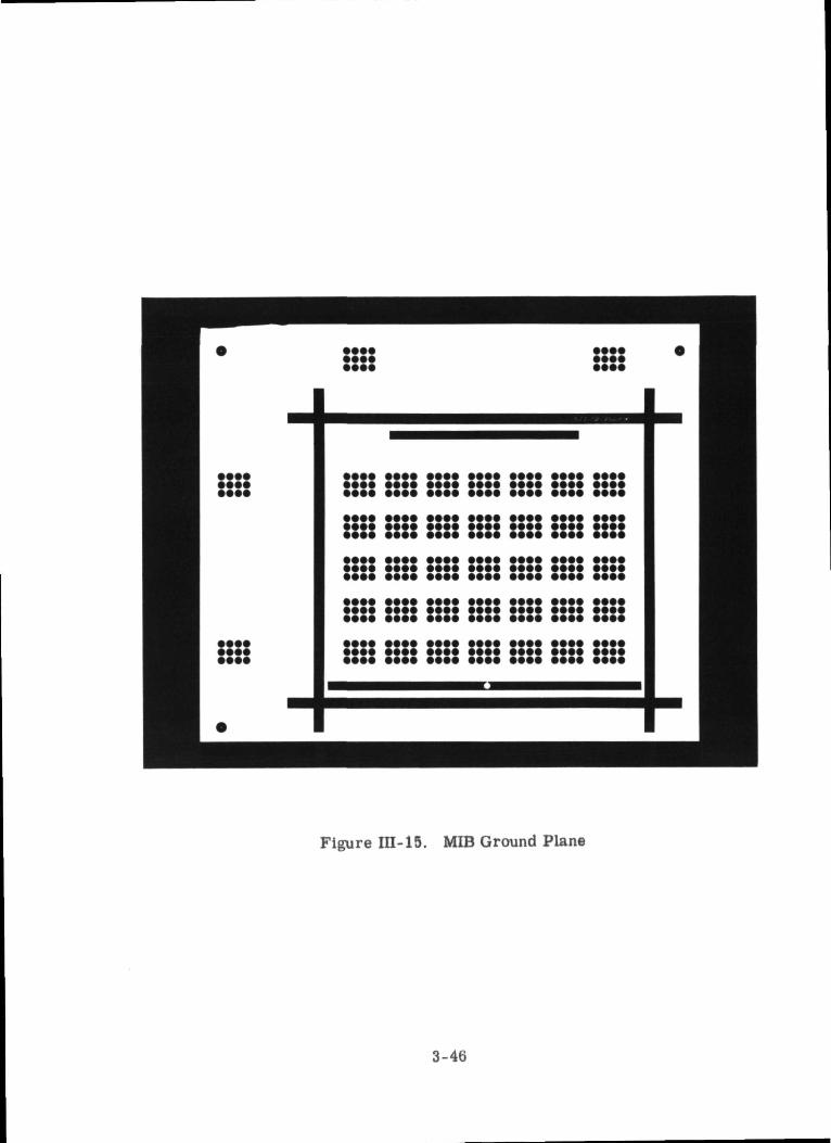
Figure III-15. MIB Ground Plane
3-46

Figure III-16. MIB Front and Rear Before Trimming
3-47

ill
IB0)
3-4
8

o•rH-4
-1
eiItai-HO
O>»(HOa0)
OO
5
3-49

Figure 111-19. Flat Cable Artwork
3-50

1
NO
IlD3i3
Q
iN3
W3
3a
9V
Sia
\ 1
£
~
=V(VI
<T
q* U««.
Z 5
MODULE SWITCHING ^
SIGNALS
<niZ -
0:5u
j£
*J- ui(/>
oO
Z K
if)
>u
jo
~
O O
rf"
O O
fl
ill (/)
f\ *j <i
03 N
—
*N
O
"• —
-to
(vi
NE CLOCKS
E) SIGNAL
-J D
ONIHO
IIMS
snnaowV
' '
OH
O
9 H
3M
Od
SX
30
TD
" dS
iOA
D
I90T "
QH
9
'
H310
SN
4 S
»
^M
310
MODULE SWITCHING (21) z
5UJ
9N
IWU
s
9
00
AIW9DO
AIVJSIGNALS (24) ^
- 1
15
^
rW3MO
d
~ID
OI9
0T '
11^~
*
*£>—
10
<r ro
=
if) i
^~
K
U
l(V
I s zX
~
oo o
^
00_
in*
CM
=
s i
cj a:
uj
N h <
§
«
0
K
a3M
Od
10
k01901 "
1
(UE) SIGNALS (54) ^1 — *
r-+• 1 p
2liJ
(0
ID
iii Z O
C ^
*
U<
3-IH .-
™ IL
) v)
I j
O
5 rf ^5
CP O
T O
L ^
*t
i -
a -nQ
M9 9
H
3MO
d
SH
0010
^QH
aaNtoii03o
SJJ3
10A
"
W3Jjna -w
9 9
U
3M
Od
sxoono'
SH
310A
'
b3Jdna'wD 9 aa
ffOd
sxoonJ"
Sd310A
"
!lK
O
T
£i z
—
zz
z8
8|U
J
b1
K
SE^<<
'_J
U)
WinO(Om<*•
S S
—
uj
m >
_J (O
UJ
Ul
18S
|2_
5«
*2
0
f- !>—
(V
) c
(LTE) SIGNALS
S LINES
DETECTION
Ui
K
O
KO
K
< U
J
' ' 1
'
SN3 PAGES- MEMORY BUFFER1 PAGE -CAPACITORS
64 16 32 28
to
^
<j
N
Q8
v S
* vsw
y
2CE
be0
oj
ON
IWIJ.
5
Os
bD
ffi G
SU
3AIM
O IX
t-i
O
"H
3
*H
0
*
3
<nS
</ST
Figure IE- 20. Computer Interconnec
3-51
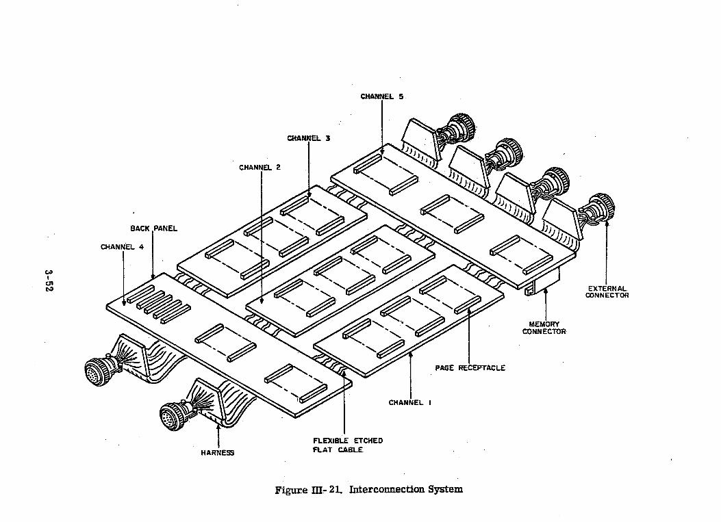
iIoo(H
caa0)
3-52
Section IV
SATURN V DATA ADAPTER
4-1

Section IV
SATURN V DATA ADAPTER
A. GENERAL DESCRIPTION
The data adapter (DA) is the input-output unit which will accompany theSaturn V guidance computer. Common technology (in terms of componenttypes, circuit module fabrication and multilayer interconnection boards (MlB))is used in the computer and DA. The DA can perform a variety ofinput-output functions and is compatible with the information rate and inter-face requirements of Instrument Unit equipment With which it must intercon-nect. It also has a growth capability to handle larger numbers of existingtypes of inputs and outputs, and to incorporate new types of functions. (Seeblock diagram, Figure IV- i .) The DA is divided into the following distinctparts:
* A digital section which buffers digital quantities such asdiscretes
• An analog section Which converts analog-to-digital anddigital-to-analog.
The power supplies which serve the DA, computer and memory arecontained in the DA. These power supplies are duplexed for reliability; thuseach supply must be capable of supplying the full current load for that volt-age. Voltage sequencing is provided where required, and power supply linescan be switched to permit single channel computer operation.
Communication with the computer is carried out through 512-kilobit-per-second serial transmission. The PIO instruction permits the specifica-tion of either input or output operations, and addresses the device to be af-fected. A single 26-bit word is transferred to the computer accumulator orfrom the accumulator or memory.
The DA employs ULD circuit modules and MIB's for circuitinterconnections. Technology which is adapted from that used in the guidancecomputer will be employed. Where low-power logic circuits are used,leadless semiconductors will be mounted on ULD's. For those applicationswhere high power dissipation is required, where precision components areneeded, or where leadless devices are not available, standard discrete com-ponents packaged in encapsulated modules will be used. This will applyparticularly in the case of power supplies, ladder networks, and cross-overdetectors.
4-2
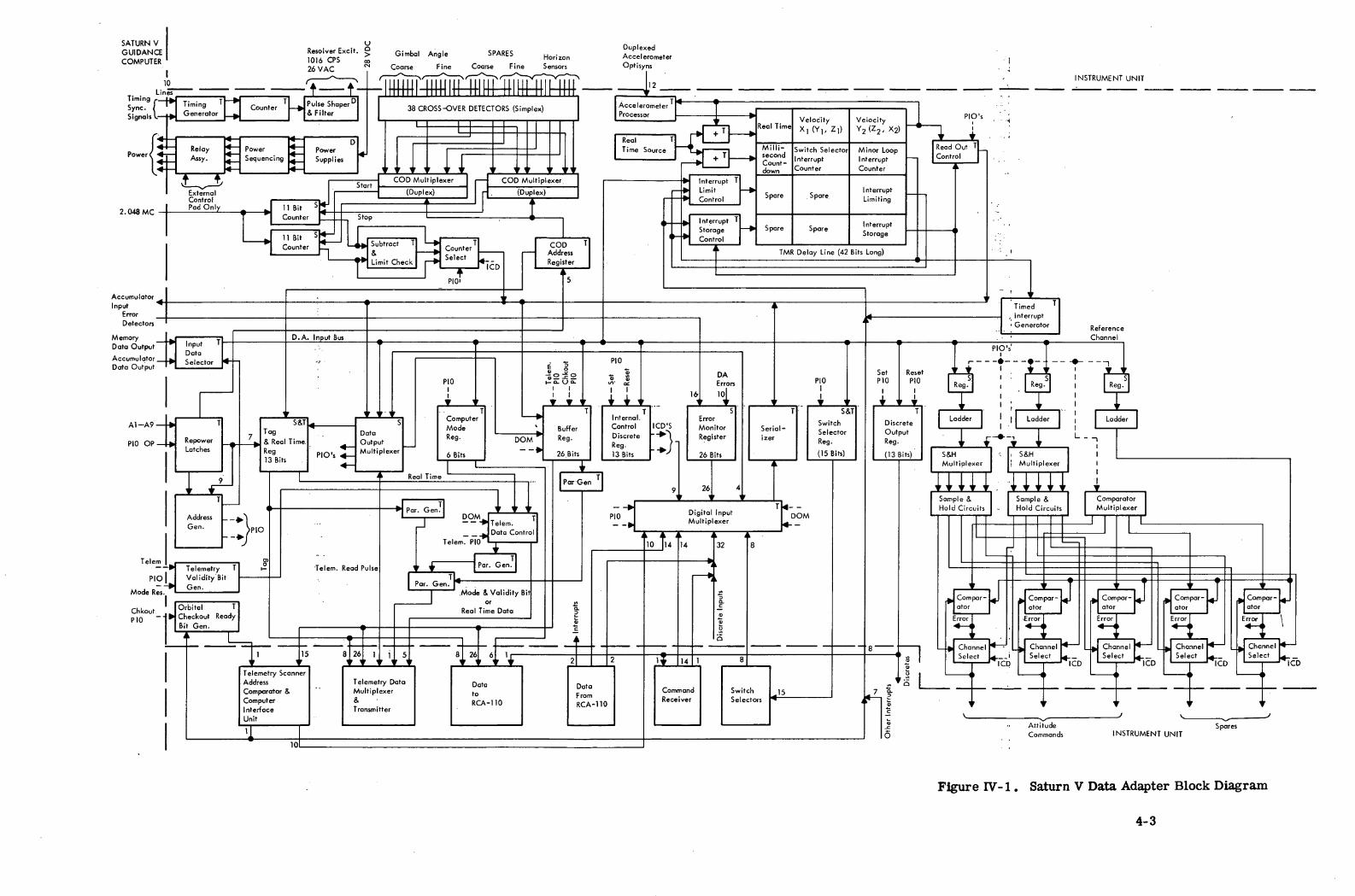
AccumulatorInput
ErrorDetectors
Memory |
Data Output
Accumulator I Data Output *^
DuplexedAccelerometerOprisyns
Resolver Excir.1016 CPS26 VAC
> Uimbal Angle -.-,..., Horizon
Coarse Fine Coarse Fine Sensors
INSTRUMENT UNIT
TimingSync.Signals
38 CROSS-OVER DETECTORS (Simplex)
Switch SelectorInterruptCounter
Mode & Validity Bitor
Real Time Data
AttitudeCommands INSTRUMENT UNIT
Spares
Figure IV-1. Saturn V Data Adapter Block Diagram
4-3
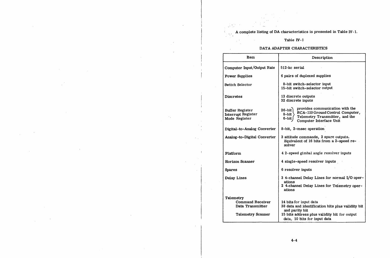
A complete listing of DA characteristics is presented in Table IV-1.
Table IV-1
DATA ADAPTER CHARACTERISTICS
Item Description
Computer Input/Output Rate
Power Supplies
Switch Selector
Discretes
Buffer RegisterInterrupt RegisterMode Register
Digital-to-Analog Converter
Analog-to-Digital Converter
Platform
Horizon Scanner
Spares
Delay Lines
TelemetryCommand ReceiverData Transmitter
Telemetry Scanner
512-kc serial
6 pairs of duplexed supplies
8-bit switch-selector input15-bit switch-selector output
13 discrete outputs32 discrete inputs
26-bit^ provides communication with the8-bit > RCA-110 Ground Control Computer,6-bit I Telemetry Transmitter, and the
J Computer Interface Unit
8-bit, 2-msec operation
3 attitude commands, 2 spare outputs.Equivalent of 16 bits from a 2-speed re-solver
4 2-speed gimbal angle resolver inputs
4 single-speed resolver inputs
6 resolver inputs
3 4-channel Delay Lines for normal I/O oper-ations
2 4-channel Delay Lines for Telemetry oper-ations
14 bits for input data38 data and identification bits plus validity bit
and parity bit15 bits address plus validity bit for outputdata, 10 bits for input data
4-4

Table IV-1. Data Adapter Characteristics (cont) .
Item Description
RCA-110
Component Count
Temperature
Reliability
Packaging
WeightVolumePower
39 data and identification bits plus validity bitfor output data,
14 bits fbr input data plus interrupt
37,000 silicon semiconductors, cermet resis-tors and other special components
60°F coolant inlet temperature, 100°C maxi-mum junction temperature allowable
0. 99 probability of success for 250 hrs;uses TMR logic, duplex special circuits, du-
plex power supplies
100 electronic page assemblies, plus specialelectronic assemblies
94 pounds2. 6 cubic feet
400 watts
B. FUNCTIONAL DESCRIPTION
1. DATA ADAPTER INTERNAL FUNCTIONS
Although the routing of data is an important DA function, the DA must alsoprocess much of the data it transmits. The internal operation of the DA maybe broken down into three main categories:
• Control data flow, including temporary storage
• Transform data into a form which is compatible with thecharacteristics of the receiving equipment
• Perform certain simple computational and logical opera-tions on the data.
The following functions are typical of those included in the first cate-gory:
• The storage of telemetry data from the computer andDA in the buffer registers
4-5

e The temporary storage of telemetry scanner addresses dur-ing orbital checkout.
o The transmission of guidance data from the computer to theanalog control computer.
Operations which require a change in the form of the data include:(Typical of those in the second category)
• Digital-to-analog, analog-to-digital, and signal level con-versions
• The formation of 40-bit RCA-110 and telemetry words from26-bit computer words
• Buffering of communications between the computer and theground-based RCA-110 to reconcile the difference in clockrates.
The DA contributes to the efficient operation of the computer by per-forming many simple, though time-consuming, logical and computationaltasks such as: (Typical of those functions performed in the third category)
• Keeping track of real time
• Decoding of operand addresses in PIO operations
2. POWER SUPPLIES
The DA contains the power supplies to drive the circuitry of the DA andthe computer. To a limited extent, power may also be furnished to interfacecircuitry in other equipment where good grounding practices dictate the need.The power is isolated from the +28 volt battery supply of the vehicle by a dc-to-dc static converter. DC output voltages will be determined by the circuitrequirements of the DA and the computer. The power supplies contain re-lays to operate the computer on the ground. These relays permit groundcheck-out of the redundant circuits to verify that all redundant functions areoperating.
3. ADDRESS GENERATOR AND TAG REGISTER
During I/O operations, the computer must select a register in the DAwhich contains or will receive the I/O data. The address of the selected reg-ister and the correct data are determined by the operand bits of the instruction
4-6
word along with the PIO control lines from the computer. These functionsare performed by the Address Generator.
4. SWITCH SELECTOR REGISTER
This register is loaded by the computer whenever the computer wishesto give commands to specific vehicle devices such as fuel valve controls.The register has a 15-bit storage capacity and is loaded by a PIO instruction.The register also controls the outputs of five switch selectors located withinthe stages of the vehicle.
The 15 bits are used as follows:
• Eight bits make up a relay tree code which is distributed inparallel to each of the five switch selectors.
• Five bits determine which switch selector will be activated.(No more than two selectors may be addressed at once.)
• One bit commands the assigned switch selector to activatethe device selected by the relay tree.
• One bit resets all switch selector relays which were turnedon by the previously described bits.
5. DISCRETE OUTPUT REGISTER
Certain functions within the vehicle, excluding those controlled by theSwitch Selector Register, are controlled by a 13-bit Discrete Output Register.An example of one function which is controlled by the Discrete Output Regis-ter is a signal to the RCA-110 and Command Receiver indicating that data hasbeen read by the computer.
To ease programming requirements for changing specific discreteswhile not affecting others, the Discrete Output Register is not loaded in thesame way as the other registers. If certain discretes are to be activated,a PIO is set up to address the "set" side of all latches in the register. Con-versely, if certain discretes are to be deactivated, another PIO selects theopposite or "reset" side of all latches in the register. The desired bits inthe register are changed by placing "ones" in the corresponding bit locationsof the data word transferred to the register from the computer while the un-changed bit positions have "zeros" in the data word.
4-7

6. DISCRETE INPUTS
Discrete inputs are signals which do hot require storage within the DA.the DA is designed to handle 32 of these inputs. Groups of these discrete in-puts are treated as words by the computer — one 26-bit word and one 8-bitword. Each word is read by the computer as requested by a PIO address.The computer reads the discretes periodically and performs the necessaryprogram steps.
Examples of discretes are:
• A "data ready" signal from the RCA-110 or the CommandReceiver.
• A "source of data" signal from the RCA-110. (If this sig-nal is not present, the "data ready" discrete is interpretedas coming from the Command Receiver.
7. SWITCH SELECTOR FEEDBACK INPUTS
When the Switch Selectors are operated as previously described, therelay tree feedback lines must be tested to assure that the tree was setproperly by the DA. Eight lines from a separate set of contacts on the relaytree contain the complement of the data word used to set the tree. Theselines are inputs to the DA which do not require storage and are addressed bythe DA in the same manner as other discrete inputs. This feedback word isseparated from the other discrete inputs so that the word may be processedmore easily in the computer when comparing it with the word used to "set"the relay tree.
8. INTERRUPT REGISTER
As a means of notifying the computer that immediate attention be givento an external operation, an interrupt line is wired from the DA to the com-puter. The Interrupt Register (Delay Line) is capable of accepting 13 differ-ent signals and storing them until the computer has acted upon them. Pre-sently, there are requirements for only eight interrupt signals. The signalsare OR1 ed together so that only one interrupt line to the computer is required.After an interrupt, the computer branches to a subroutine to read the InterruptRegister by means of a PIO operation. A computer analysis is then made,testing the highest priority bit positions first in case more than one interruptsignal is stored in the register. During this testing, the computer stores thecontents of the memory address register and the instruction counter andbranches to an interrupt subroutine. While in this subroutine, the computerwill not recognize further interrupts. The next to last instruction of the interrupt
4-8
subroutine is a PIO addressed to the Interrupt Register to reset the particu-lar bit causing the interrupt. The hardware provides a time delay to preventfurther immediate interrupts from the same source. The source must disap-pear and return before another interrupt will be honored from that source.This will prevent slow-acting devices such as relays from regenerating inter-rupts while they are being activated by discrete outputs which occur duringthe interrupt subroutine. Each interrupt signal must be at least 84 us. dur-ation to assume storage in the delay line.
The computer is also capable of inhibiting the interrupt,as commandedby the program,with PIO instructions whenever the function of the subroutinewarrants this precaution. However, a few of the inputs will bypass this in-hibit control; these latter inputs will be caused by functions which require thehighest priority of attention. The TM Scanner Address Comparator and theRCA-110 each have one input to the Interrupt Register.
9. BUFFER REGISTER
The Buffer Register provides storage for a 26-bit word and is loadedby PIO operations or the Data Output Multiplexer for DA data telemetry op-erations. It provides part of the interface required for transferring data tothe telemetry transmitter and/or RCA-110. It also stores addresses to becompared in the Telemetry Scanner Address Comparator during orbital orground check-out. It provides parallel outputs to all of these external sys-tems simultaneously. These systems read data from this register asynchro-nously with respect to computer timing.
10. MODE REGISTER
The Mode Register is similar to the Buffer Register and other one-word registers loaded by the computer. It provides storage for a 6-bit com-puter word which defines the computer mode of operation. While communi-cating with the RCA-110 these six outputs are read in parallel by the RCA-110.The Telemetry Data Multiplexer reads four of these outputs when transmittingcomputer telemetry words, but real time information data will be substitutedfor these bits when DA data is transmitted.
11. VALIDITY BIT GENERATOR
Since the Telemetry Data Multiplexer addresses the DA asynchronouslywith respect to computer timing, it is possible for telemetry words to beread while they are being changed by PIO operations. However, data read atthis time is invalid. Also, since the Buffer Register is used to store addressesof other telemetry system parameters during orbital check-out, this data wouldbe invalid as telemetry outputs from the DA.
4-9

Therefore a signal must be included in the telemetry word which indi-cates the validity of the word. The Validity Bit Generator performs thisfunction. Data will be invalid any time the Computer Mode Register, TagRegister and Buffer Register are being loaded. It will also be invalid whenthe Buffer Register contains orbital check-out address information.
12. READY-BIT GENERATOR
During orbital check-out the computer examines various parameterswhich are monitored by the telemetry system. The computer obtains one ofthese inputs by sending a Telemetry Scanner address to the Buffer Register.This 15-bit address is compared in the Telemetry Scanner Address Com-parator. When comparison occurs the telemetry word is stored in a 10-bitregister which is read by the DA. Another line interrupts the computer tonotify it that data is available.
Since the Buffer Register is continuously connected to the TelemetryScanner Address Comparator as well as the Telemetry Data Multiplexer andRCA-110 interface, it is necessary to indicate to the Address Comparatorwhen the Buffer Register data is ready for comparison. This is the functionof the Ready Bit Generator. The "ready" bit is turned on after the 15-bitaddress is loaded into the Buffer Register, under control of a special PIOinstruction. The bit remains on until after the address has been comparedand the 10-bit data word has been stored; it is turned off by the line causingthe computer interrupt.
13. PARITY GENERATOR
To help ensure that computer data sent out over the RF telemetry linkto ground equipment is received without error, a parity bit is included ineach 40-bit data word sent out by the DA.
The telemetry data word is formed from three subwords plus a validitybit. The validity bit however, is not included in the parity check. Odd parityis used. This means that,excluding the validity bit, all the "ones" in thethree subwords plus the parity bit will add up to an odd number. The easiestway to generate total parity is to generate an individual parity bit for each sub-word. The three parity bits are then checked for total parity and a resultantparity bit is generated.
14. INTERNAL CONTROL DISCRETE REGISTER
Certain functions within the DA must be controlled by the computer. A13-bit register, very similar to the Discrete Output Register, is included toprovide these controls.
4-10

Some of the functions of these discretes are:
• Control switching of duplex delay line channels
• Selection of the duplex analog output channels to be used
• Control to inhibit certain interrupts.
15. PIO DIGITAL INPUT MULTIPLEXER AND SERIALIZER
Excluding the computer, all digital input words except accelerometerinputs occur in parallel form. Since the computer can read only one groupof inputs (one word) at a time, the group of inputs selected by the PIO re-quest is switched to a single Serializer which converts the parallel inputs tothe 512-kc serial bit rate. The output of this Serializer is fed to the accum-mulator input data bus. The PIO Multiplexer provides the necessary switch-ing for the input word selected by the computer.
Data from the RCA-110 and the Command Receiver have the same ad-dress. If the RCA-110 is connected to the system, a discrete input indicatesthis and provides a control gate to inhibit inputs from the Command Receiverwhile allowing inputs to come from the RCA-110. The converse of this istrue if the RCA-110 is not connected into the system.
16. TMR DELAY LINE
The use of glass delay lines in a TMR configuration has effected sig-nificant component savings and resultant reliability improvements in the DA.They replace several latch registers that would otherwise be required forthe functions being implemented.
This TMR delay line has been organized around computer timing suchthat the information it contains remains synchronized with the computeroperation cycle. The total circulation time of the delay line and its associ-ated electronics will be equal to the basic computer instruction cycle timeof 82. 03 microseconds (42 bit times). The delay line will be divided intothree 14-bit word times corresponding to the three computer phase times.Furthermore, the four clock times into which each computer bit time isdivided will be used to time-share the delay line among four "channels" of512-kilocycle serial information. Hence, a total of 12 14-bit words can bestored in a single delay line by operating the line at 2. 048 megacycles persecond. Figure IV-2 illustrates how these word locations will be used.
4-11

in performing a PIO operation, the computer sends out or looks forinformation only during phase-times "B" and "C." Real time has been as-signed to a phase "A" word time. This is done to facilitate the use of realtime information in the Data Output Multiplexer (DOM). However, real timewill be made available to the computer during phase "B" via the multiplexerregister arid the serializer latch.
the velocity accumulations, which are the processed outputs of theaccelerometer optisyns, are arranged in such a manner as to provide duplexredundancy, matching the duplexed optisyns, in the TMR delay line. One linewill contain outputs Xj and ¥2, another will accumulate Yj and Z2, while stillanother will process Zj andX^- When the computer calls for a given velocityaccumulation, it will receive the processed output of one of the optisyns on theselected accelerometer in phase "B" and the output of other optisyn oh thesame accelerometer during phase "C. " These two values will be processedseparately in the computer such that any one of the delay lines or any optisyncould fail without failing the system.
No initialization has been provided for this delay line. The real timeaccumulation is voted upon in TMR voters during every circulation, so thevalues in all three lines will always agree. The duplex operation of the ac-celerometer processors does not allow voting, so there is no guarantee thatthe absolute value of the two readings will agree. Inasmuch as it is the changein velocity between readings that is of interest, and since the duplexed out-puts are processed separately in the computer, it is assumed that the extracircuitry required for initialization is unnecessary. Real time is accumu-lated in 246. 1-microsecond increments, while the least significant bit in thevelocity measurement has a weight of 0. 05 meters per second.
The delay channel whose bits are written at Y time is used to timethree functions in the data adapter/computer system. In phase "A, " a timedelay of approximately 1 millisecond duration for use in the D/A converteris generated by counting 12 circulations of the delay line. In phase "B, "time to go until the next computer interrupt for the switch selector functionis counted down, while the time remaining before the next minor loop iscounted down in phase "C." These two countdowns occur at the rate of onecount every 0.4922 millisecond, and they generate an interrupt when theypass through zero. The length of the count is determined by the computer,which loads a value of time-to-go to indicate each count.
4-12

wClock
Clock
YClock
ZClock
Phase A
Spare
Spare
MillisecondCountdown
RealTime
Accumulation
Phase B
Spare
Spare
SwitchSelector
InterruptCountdown
VelocityAccumulationX^Yj, Zj)
Phase C
InterruptStorage
InterruptLimiting
MinorLoop
InterruptCountdown
VelocityAccumulationY2(Z2, X2)
ReadChannel
WriteChannel
WriteChannel
ReadChannel
Figure IV-2. Use of Word Locations
Computer interrupts are stored in phase "C" of channel "W. " Oncethe computer recognizes an interrupt, it sets the corresponding bit in phase"C" of channel "X" and resets this bit in channel "W. " The associated cir-cuitry prevents a new interrupt from being recognized in this bit positionuntil the previous interrupt has disappeared. The only constraint, there-fore, on the length of the interrupt signal is that it lasts for at least 82.03microseconds.
In Figure IV-2 it can be seen that four spare words are left in channels'W" and "X. " Channel "W" may be conveniently read by the computer, whilechannel "X" may be conveniently written into from the computer. As manyas three of the normal 14 bits may have to be sacrificed if it is desired to useeither of these two channels in the opposite manner.
4-13

17. TELEMETRY MONITORING OF DATA
a. Digital Data Monitoring
The PCM telemetry system to be used for monitoring digital data willaccept 40-bit words at an asynchronous rate of 240 words per second. Specialbuffering and control logic must be provided in the data adapter to tempor-arily store input and output data occurring at instantaneous rates greaterthan 240 words per second.
The telemetry monitoring system will telemeter all significant dataadapter inputs and outputs read or written by PIO operations. In addition,other important data available only in the computer will be telemetered.This data will also be transferred by PIO operations. The only Pip opera-tions that will not be telemetered are those caused by the timed interruptoperations.
It is assumed that the computer will not send out telemetry data duringthe minor loop of the operational program nor will its telemetry output exceed100 words per second.
Assuming four gimbal angle inputs, each at a rate of 25 per second,and three attitude command outputs at the same rate could mean an additional175 PIO's per second. Added together, these would exceed the allowabletelemetry rate of 240 words per second. However, since gimbal angles andattitude commands are short words of less than one syllable, they can becombined in a delay line register so that two PIO words make up one tele-metry word. This would reduce the effective number of inputs and outputsof this type to 87-1/2 telemetry words per second.
, Other PIO's have been assumed to occur at the following rates:
Computation Mode Register 0. 2/secReal Time 5/secCOD Error Inputs I/secCommand Receiver 4/secSwitch Selector (Normal Operation) 20/secDiscrete Inputs 8/secError Monitor Register I/sec
4-14

Internal Control Discretes 0. 2/secOptisyn Inputs 6/secDiscrete Outputs 0. 2/secHorizon Sensors 8/secMinor Loop Interrupts (Timed) 25/secSwitch Selector Interrupts (Timed) 20/secOther Interrupts I/sec
Total 99.6/secOf this total, time interrupts account for 45/sec. Excluding these, which willnot be telemetered, the total reduces to 54. 6/sec.
In summary, the estimated number of telemetry words generated eachsecond is as follows:
Computer 100/secGimbal Angles and Attitude Commands 87. 5/secOther PIO's, excluding Timed Interrupt 54. 6/sec
Total telemetry operations 242. I/sec
For digital outputs, data will be monitored at the interface of the dataadapter to determine whether the correct signals were sent to the externalequipment. This applies to the switch selector and discrete output registers.Each have serial inputs and parallel outputs. The switch selector registerhas 13 address bits, one read command, and one reset bit, while the dis-crete output register has 13 bits. The read command and reset bits of theswitch selector are eliminated from telemetry making the outputs of bothregisters one-syllable words. This allows the formation in a delay line ofa 26-bit word containing the serial input to one of these registers and theoutput of the register, and in turn requires loading the data output registerand the address bits of the switch selector register during phase "B" of thePIO operation. The parallel outputs will then be serialized through thedigital input multiplexer and stored in the delay line during phase "C" of thePIO operation. The internal control discrete register, which has no externalinterface, will be monitored in the same way.
A data output monitor (DOM) (Figure IV-3) provides the additionaldelay line buffer storage and control logic needed to handle all digital tele-metry words except the computer telemetry words previously mentioned.
4-15

s(DOOO*o>a
t%m <nIsS
«
fcQ)
4-16

Computer telemetry words will be loaded directly into the 26-bit bufferregister in the DA by PIO's and, along with four bits from the mode registerand eight bits from the tag register, a validity bit and a parity bit will betransmitted in parallel to another 40-bit core buffer in the telemetry equip-ment. The DOM also shares this hardware, except for the mode register andthe validity bit generator. When a synchronizing pulse occurs, indicatingthat a word has been read by the telemetry equipment, a new word is trans-ferred from the DOM buffer into these registers in preparation for the nexttelemetry "read" operation. If a computer telemetry PIO takes place beforethe DOM word has been read, it will have priority and computer data will besubstituted for DOM data. The DOM will reload the same data for trans-mission as soon as the computer word has been transmitted. (Refer to thetiming chart, Figure IV-4. )
To provide a meaningful tag for those telemetry words assembledfrom two PIO words, a fixed format must be established for the assembledwords. A special delay line buffer will be used to provide this function thus,data sorted in this delay line might be as follows:
ChannelW
Channel X
Channel Y
Channel Z
Phase A
Tag A RealTag B Time
Tag C RealTag D Time
Tag E RealTag F Time
Tag G RealTag H Time
Phase B
AttitudeCommand A
AttitudeCommand B
AttitudeCommand C
Spare
Phase C
Fine PitchCoarse Pitch
Fine YawCoarse Yaw
Fine RollCoarse Roll
Fine Redun. YawCoarse Redun. Yaw
In addition to the gimbal angles shown, horizon sensor and other CODinputs may be added. Tags will always be generated from the address storedin the COD address generator, which is required to select the resolver input.Unique groups of tags will not only define the COD input but also the attitudecommand stored in the same channel.
There is no problem in tagging the following input and output PIO words:
Command ReceiverSwitch Selector RegisterDiscrete InputsDiscrete Outputs
Error Monitor RegisterInternal Control DiscretesOptisyn InputsInterrupt Register
4-17

c[Zc.d.c
•==«=l=_
Jl
Z o
11"Jl
Z 0
C
S0oS -h
Z Qy
'
Oo• 0
O
Dtrt
O
d
50oJltzs8>
o
hcsoa$ o
Z Q
Ct=C
15oa«oo';
5O3
c
ia01bc*
3'c
1»(J 'ij3|
Q«?
*|i-
!,>1 C
7°5
•?
°
1SOo1 sI £
iS0o
1 I
u '8
1
15
t'1§••sO
b 1
s: J
4-1
8

Therefore, another delay line buffer will store these parameters. Channelsof this delay line will not be allocated to certain parameters, but will beloaded as available after previously loaded data has been transmitted. Theparameter tags will be formed partially from the operand address of the PIOoperation and will be stored in the phase "A" portion of the delay line asbefore.
Two delay lines will provide storage for eight 26-bit telemetry words,plus tag and real time data. When the computer is not generating telemetrydata, these words will be selected in sequence by delay line channel for trans-mission. If there are no valid data in a selected channel, the counter willadvance until valid data are located. A 3-bit sequence counter will be re-quired to select channels. The counter will be advanced by a synchronizingpulse from the telemetry equipment every 1/240 second (4, 17 millisecond)if the computer did not load a telemetry word since the last sync pulse. Ifthe latter occurs, the counter does not advance and the same data are re-loaded for transmission.
With eight words of storage, some data words will be buffered8 x 4. 17 milliseconds (33. 4 milliseconds) or longer if the DOM is interruptedby computer telemetry operations. It is therefore desireable to include ad-ditional data along with the tag information to indicate when the data was loadedin the buffer delay line. Five bits from the real time counter in the D. A. willbe added to phase "A" data. The low order bit represents an increment of2 milliseconds so real time can be expressed over a range of 64 milliseconds.These real-time increments, when correlated with timing information gen-erated by the telemetry system, will pin-point data generation time to within2 milliseconds. To add these five bits of time information, it is necessary todelete other data making up the 40-bit telemetry word. To prevent any am-biguity of associating real time with the short data words in the special delayline, this line might be limited to minor loop data such as platform gimbalangles and attitude commands. Telemetry transmissions from this line couldthen be inhibited during the minor loop and allowed only in the major loop.The four mode bits and one validity bit used with computer telemetry wordswill be deleted. This would be done for DOM telemetry operations only.
When processing this data on the ground, it is possible to distinguishbetween DOM and computer telemetry words by looking at tag bit 8. Thepresence of a bit in this position indicates that the data originated in the com-puter. Otherwise the data was DOM-generated. Tables IV-2 and IV-3 pre-sent details on PIO and tag bit coding.
4-19
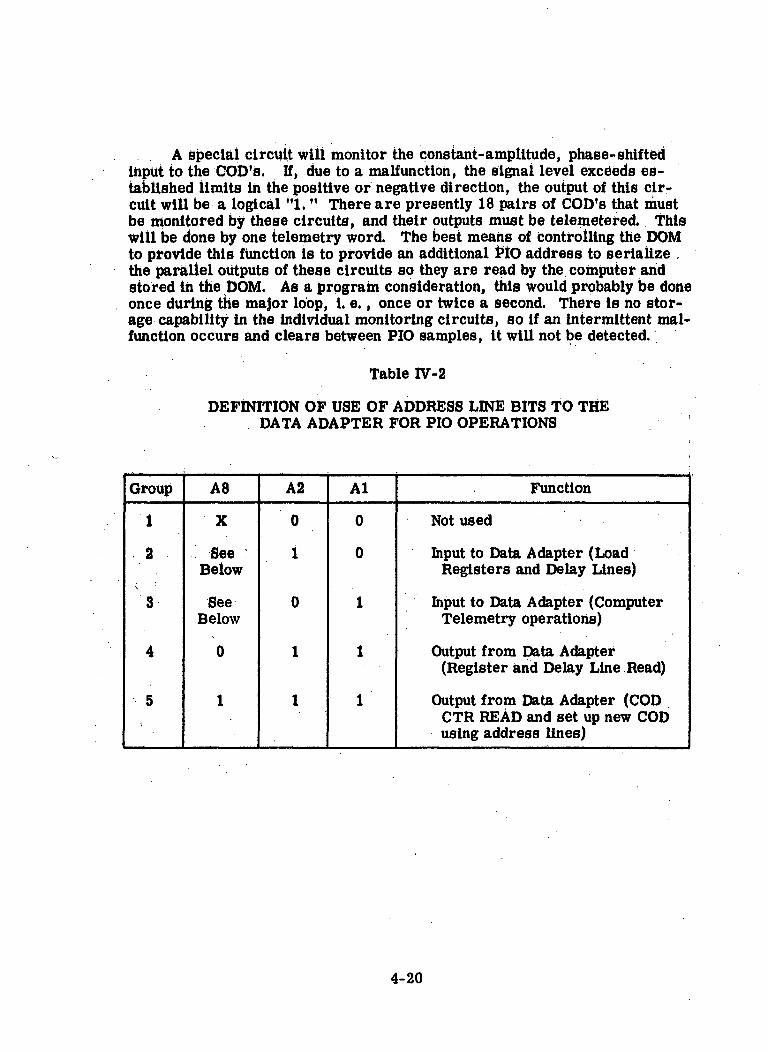
A special circuit will monitor the constant-amplitude, phase-shiftedinput to the COD's. If, due to a malfunction, the signal level exceeds es-tablished limits in the positive or negative direction, the output of this cir-cuit will be a logical "1. " There are presently 18 pairs of COD's that mustbe monitored by these circuits, and their outputs must be telemetered. Thiswill be done by one telemetry word. The best means of controlling the DOMto provide this function is to provide an additional PIO address to serialize ,the parallel outputs of these circuits so they are read by the. computer andstored in the DOM. As a program consideration, this would probably be doneonce during the major loop, i. e., once or twice a second. There is no stor-age capability in the individual monitoring circuits, so if an intermittent mal-function occurs and clears between PIO samples, it will not be detected.
Table IV-2
DEFINITION OP USE OF ADDRESS LINE BITS TO THEDATA ADAPTER FOR PIO OPERATIONS
Group
1
2
3
4
5\
A8
X
SeeBelow
SeeBelow
0
1
A2
0
1
0
1
1
Al
0
0
1
1
1
Function
Not used
Input to Data Adapter (LoadRegisters and Delay Lines)
Input to Data Adapter (ComputerTelemetry operations)
Output from Data Adapter(Register and Delay Line Read)
Output from Data Adapter (CODCTR READ and set up new CODusing address lines)
4-20

Table IV-2. Definition of Use of Address Line BitsTo The Data Adapter For PIO Operations (cont)
A3
A4
A5
A6
A7
A8
A9
Group 1
NotUsed
Group 2
!
Address
SeeBelow
A8 A90 0 M MEM
° * ACC1 01 1 R MEM
64 ACC32 RES MEM32 MAIN MEM
Group 3
Address
SeeBelow
A8 A90 00 1 ACC1 01 IRES
MEM
96 ACC32 RES MEM
Group 4
Address
0
Not Used
Group 5
Address
1
Not Used
Bit A8 is used to recognizeCOD group.
4-21

Table IV-3
DEFINITION OF TAG CODE TO BE USED WITH TELEMETRY
tag Bit 1
2
3
4
5
6
7
8
PIO Group 2
; 0
1
A3
A4
A5
A6
A7
0
PIO Group 3
A8
A9
A3
A4
A5
A6
A7
1
PIO Group 4
1
0
A3
A4
A5
A6
A7
0
PIO Group 5
0
0
A3
A4
A5
A6
A7
0
Al, A2, and A8 are decoded in the DA to determine what goes into tagbit 1, 2, and 8 positions. A "1" in tag bit 8 position indicates that thecomputer is the source of data. For a "0", the DOM is the source. ForDOM data, tag bits 3 through 7 identify the word or register addressed inthe DA and are the corresponding operand address bits of a PIO instruction.Tag bits 1 and 2 identify whether the data is an input, output, or COD word.Computer telemetry words are identified by operand address bits A3 throughA9.
4-22
be a logical "1". There are presently 18 pairs of COD's that must bemonitored by these circuits, and their outputs must be telemetered. Thiswill be done by one telemetry word. The best means of controlling the DOMto provide this function is to provide on additional PIO address to serializethe parallel outputs of these circuits so they are read by the computer andstored in the DOM. As a program consideration, this would probably bedone once during the major loop, i. e. once or twice a second. There is nostorage capability in the individual monitoring circuits, so if an intermittentmalfunction occurs and clears between PIO samples, it will not be detected.
b. Analog Data Monitoring
Certain data in the data adapter will be monitored by the analog inputchannels to the PCM telemetry system. These include the following:
(1) Unfiltered 28 VDC input to the DA(2) Filtered 28 VDC output from the DA(3) +6 V from power supply No. 1(4) +6 V from power supply No. 2(5) +12 V(6) +20 V(7) -3 V(8) Attitude command "A"(9) Attitude command "B"
(10) Attitude command "C"(11) Spare ladder output "A"(12) Spare ladder output "B"(13) Computer thermistor output "A"(14) Computer thermistor output "B"(15) DA thermistor output "A"(16) DA thermistor output "B"(17) Optisyns(18) Resolver excitation
For 1 through 12 of the previous list, these signals must be scaleddown in most cases to be compatible with the full scale range of 0 to 5 VDCfor the telemetry system inputs. No interface circuits are required toconnect the thermistor outputs into the telemetry system. Each thermistorwill provide two output lines to telemetry. In addition, all computerthermistor circuits will be routed to telemetry through the DA.
4-23

C. ANGLE MEASUREMENT
The instrumentation used is capable of measuring shaft angles in digitalform to an accuracy of approximately one part in two thousand. This requiresan analog-to-digital conversion of eleven bits. To accomplish measurementsand conversion of the shaft angles, a time-duration measurement is used.This is accomplished by connecting a resolver in such a manner that two sig-nals will be generated to switch a high-frequency counter on and off. The re-resultant count, after a measurement cycle, represents the angle in binaryform.
The basic principle of operation can be seen by considering the sum ofthe constant amplitude and frequency sine wave modulated by the cosine andsine respectively of the variable of interest. This is:
er = (E sin wt) cos 9 + (E sin wt) sin9 .
The sum can be modified to a useful trigonometric form by shifting one of thewaves by 90 deg. Thus
er = (E sin wt) sin 9 + E sin (wt + " ) cos 8
where, by a standard identity,
er = E cos (w t - 9).
These operations are carried out by the resolver and its associated cir-cuitry by feeding an excitation signal to the resolver as shown in Figure IV-5.The input sinusoid is multiplied by the sine and cosine of the angular rotationof the rotor with respect to the stator of the resolver. A phase shifting net-work connected to the two rotor windings causes their outputs to differ inphase by 90 deg.
4-24
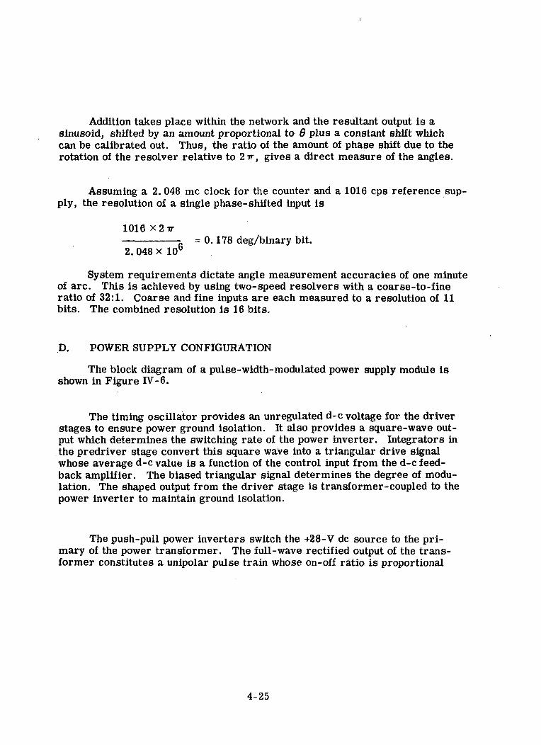
Addition takes place within the network and the resultant output is asinusoid, shifted by an amount proportional to 9 plus a constant shift whichcan be calibrated out. Thus, the ratio of the amount of phase shift due to therotation of the resolver relative to 2ir, gives a direct measure of the angles.
Assuming a 2. 048 me clock for the counter and a 1016 cps reference sup-ply, the resolution of a single phase-shifted input is
1016X2 ir= 0.178 deg/binary bit.
2. 048 x 10b
System requirements dictate angle measurement accuracies of one minuteof arc. This is achieved by using two-speed resolvers with a coarse-to-fineratio of 32:1. Coarse and fine inputs are each measured to a resolution of 11bits. The combined resolution is 16 bits.
D. POWER SUPPLY CONFIGURATION
The block diagram of a pulse-width-modulated power supply module isshown in Figure IV-6.
The timing oscillator provides an unregulated d-c voltage for the driverstages to ensure power ground isolation. It also provides a square-wave out-put which determines the switching rate of the power inverter. Integrators inthe predriver stage convert this square wave into a triangular drive signalwhose average d-c value is a function of the control input from the d-c feed-back amplifier. The biased triangular signal determines the degree of modu-lation. The shaped output from the driver stage is transformer-coupled to thepower inverter to maintain ground isolation.
The push-pull power inverters switch the +28-V dc source to the pri-mary of the power transformer. The full-wave rectified output of the trans-former constitutes a unipolar pulse train whose on-off ratio is proportional
4-25

d a
4-26
+ 28 VDC± 3V. INPUT
TIMINGOSCILLATORANDUNREG. P.S.
ISOLATED DC POWER
TIMING
CONTROLPRE-DRIVER DRIVER POWER
INVERTER
AMP\
REGULATEDD.C. O-OUTPUT
-OREF.
Figure IV-6. Pulse-Width-Modulated Power Supply ModuleBlock Diagram
to the circuit losses and inversely proportional to the -t-28-V dc line voltagevariations. The single section LC filter smoothes the modulated pulses intoa low-ripple, regulated d-c voltage. Any variation in the average value ofthe output voltage is sensed by the feedback amplifier, and the error signal isused to control the power inverter pulse width.
The Saturn V guidance computer and data adapter require five d-c sup-ply voltages. To handle the large current requirements of one of these sup-plies (+6 volts) with available high-quality components, this load is split andis furnished by two independent sources. The power supply subsystem con-sists of 12 power converter modules and 24 feedback amplifiers arranged tofurnish 6 highly reliable power sources.
The efficiency of this complete cl-c power system which uses duplexedmodules will be approximately 60 percent. The efficiency of a comparabledual series-regulator power supply is estimated to be about 30 percent. Thebetter efficiency of the pulse-width-modulated regulator is due primarily tothe absence of any linear elements in series with the power source.
4-27

E. SPECIAL CIRCUIT DESIGN
Most of the digital circuits used in the DA are identical to those used inthe computer. Some special circuits are needed to accommodate the inter-faces to external equipment. Two special circuit designs are discussed inthe following paragraphs;
1. 28-VOLT BUFFER INTERFACE CIRCUIT
A buffer circuit is used to convert the 28-volt digital input signals to6-volt ground referenced signals, compatible with the DA logic circuitry.Since an input noise of 4 volts is expected, an inverter with input noise re-jection of at least 7 or 8 volts is used. Either component redundant or TMRtechniques can be used to obtain reliability.
2. RESOLVER FREQUENCY SOURCE
The 1016 cps frequency needed to drive the resolvers is obtained bycounting down from computer timing pulses. This is accomplished with athree-stage ring counter followed by a latch. (See Figure IV-7.)
CLOCK PULSE-
PHASE PULSE
RINGCOUNTER(3 BIT)
LATCH CLIP FILTERAMPLIFY
LEVELSENSE
Figure IV-7. Resolver Frequency Source-Block Diagram
A variable clipper controls the amplitude of the 1016 cps square wave ob-tained from the counter. The clipping level is set by level-sensing detector-amplifier circuitry. The fundamental component of the square wave is ob-tained by filtering, and is amplified to a 26-volt level which is adequate todrive the resolvers. The 26-volt level is maintained by an amplitude sensi-tive feedback circuit. The harmonic content is reduced by filtering. Thisfiltering is accomplished by incorporating frequency selective feedbacktechniques in the amplifier circuitry.
4-28

The resolver frequency source is duplexed in a sense, i.e., each sourcewill supply power for half of the resolver inputs in such a manner that fineand coarse resolver excitation for any input parameter is not supplied by thesame source. Since fine and coarse inputs serve as a backup for each other(under the proper program control),duplex redundancy is used for the excita-tion source.
F. PACKAGING
A packaging design similar to that employed for the computer is usedfor the data adapter. ULD's mounted on pages contain the majority of thedigital circuits. Potted cordwood-type Circuit Modules mounted on MIB'sare used where high-dissipation circuits or circuits requiring large precisioncomponents are needed, Figure IV-8. Ten CM's are mounted on a pagewhich contains electronics on one side only. The CM pages require themounting space of three ULD pages. The area under the cantilevered CMpages is used for interconnection between backpanels. The layout of the DApackage is shown in Figure IV-9.
4-29

Figure IV-8. Data Adapter Circuit Module
4-30

_^j r— -j
00 ,r i
ooOO i 1oooo L }• m l — — 1
-
1 1n
II
i -
rIIVI
IIL
PI
^-to>—
ooooof r*
t
i
i
4 15 f
-
riAX
1 II 1 nu
Ijl/ ^ L-
POWER SUPPLIES
I'lLOGIC PAGES |Jj
| ij
•'""N .ISAMPLING"^ ^ \\ j (CAPACITORS/ \^ /
LOGIC PAGES tjjIn
n1C
=6
TERMINAL BOARDS
30 MAX
IV
28
Figure IV-9 . Data Adapter Packaging Layout
PAGES-REO'D27 CORDWOOD70ULD
TOTAL SPACESAVAILABLE =17833 CORDWOOD79 ULD
4-31/32

Section V
LABORATORY TEST EQUIPMENT
5-1
Section V
LABORATORY TEST EQUIPMENT
A. GENERAL
Four machine types are used to test the computer and data adapter.These machine types are as follows:
• Saturn V Computer Manual Exerciser (ACME)• Saturn V Data Adapter Processor Tester (ADAPT)• Saturn V Test and Evaluation Console (ASTEC)• Saturn V Test and Operational Monitor (ATOM)
The ACME tests the computer as a unit, monitoring the computer as itruns a special program that exercises the hardware to the maximum possibleextent. The ACME is not designed to be used with computer operational pro-grams, but is used in conjunction in hardware acceptance and qualificationtesting.
The ADAPT tests the DA. It is capable of (1) exercising the interfacebetween the computer and DA, and (2) simulating the inputs to the DA andaccepting its outputs, both digital and analog. The ADAPT will be used inproduction build-up, acceptance testing and qualification testing of the DA.
The ASTEC can test the computer alone, the DA alone, and the com-puter/DA combination. The ASTEC is used for computer and DA hardwarecheck-out and for operational program check-out and acceptance tests. TheASTEC is also used in troubleshooting the computer and DA by implementingmalfunction isolation techniques.
The ATOM facilitates analysis of the computer and DA. It enables anoperator to observe either the contents of the accumulator or the memoryregister at a particular instruction address time and perform control opera-tions on the computer. The ATOM will be used in an Instrument Unit bread-board for operational testing.
B. MACHINE CONFIGURATION
The ACME tester (see Figure V-l) consists of two standard IBM double-cube modules bonded together and a single-cube module. One of the double-cube modules contains a high-speed paper-tape reader and its controls. Thereader is used for computer memory loading and verification. The otherdouble-cube module contains control switches and visual displays of computerregisters and test points. The electronics and power supplies for ACME,
5-2
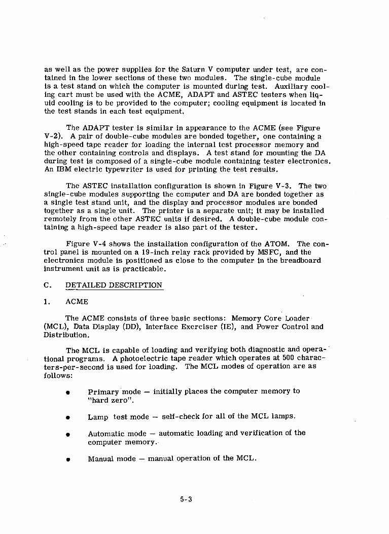
as well as the power supplies for the Saturn V computer under test, are con-tained in the lower sections of these two modules. The single-cube moduleis a test stand on which the computer is mounted during test. Auxiliary cool-ing cart must be used with the ACME, ADAPT and ASTEC testers when liq-uid cooling is to be provided to the computer; cooling equipment is located inthe test stands in each test equipment.
The ADAPT tester is similar in appearance to the ACME (see FigureV-2). A pair of double-cube modules are bonded together, one containing ahigh-speed tape reader for loading the internal test processor memory andthe other containing controls and displays. A test stand for mounting the DAduring test is composed of a single-cube module containing tester electronics.An IBM electric typewriter is used for printing the test results.
The ASTEC installation configuration is shown in Figure V-3. The twosingle-cube modules supporting the computer and DA are bonded together asa single test stand unit, and the display and processor modules are bondedtogether as a single unit. The printer is a separate unit; it may be installedremotely from the other ASTEC units if desired. A double-cube module con-taining a high-speed tape reader is also part of the tester.
Figure V-4 shows the installation configuration of the ATOM. The con-trol panel is mounted on a 19-inch relay rack provided by MSFC, and theelectronics module is positioned as close to the computer in the breadboardinstrument unit as is practicable.
C. DETAILED DESCRIPTION
1. ACME
The ACME consists of three basic sections: Memory Core Loader(MCL), Data Display (DD), Interface Exerciser (IE), and Power Control andDistribution.
The MCL is capable of loading and verifying both diagnostic and opera-tional programs. A photoelectric tape reader which operates at 500 charac-ters-per-second is used for loading. The MCL modes of operation are asfollows:
• Primary mode — initially places the computer memory to"hard zero".
• Lamp test mode — self-check for all of the MCL lamps.
• Automatic mode — automatic loading and verification of thecomputer memory.
• Manual mode — manual operation of the MCL.
5-3

oo8
Ooooin
D]
1U4
§K'
o<COID<t
««- I
i-510 OT
10 hiO
5
u 5
2E UJ
p? -u) «- wo
SEn
utZ«l(tu.
<n(M
5-4
RHEEM PAPER TAPEREADER
DATAADAPTER
IBM SELECTRICOUTPUT TYPEWRITER
Figure V-2. ADAPT Installation Outline Drawing
5-5

on
.
5-6

5-7

The basic modes of operation of the DD are as follows:
Switch-selected data inputSpare data probe data inputRepeat-displaySingle-displaySingle-stepAutomatic/manual restartExternal oscilloscope synchronizationExternal oscilloscope markerLamp test
The IE provides signal inputs to the data adapter-computer interface.With these inputs, the internal demonstration program exercises the com-puter hardware to the maximum extent. However, the IE is not used withoperational programs.2. ADAPT
The ADAPT contains circuits which interface with all DA externalconnections. It provides stimuli to DA inputs via a multiplex and distributor,and receives data and control pulses from DA outputs. Testing is controlledby a digital processor which has a magnetic core memory and a simplifiedinstruction set.
The processor directs the tests to be performed by reading out digitalinformation from its memory for DA inputs, and comparing DA outputs withprestored results. Data may also be recorded in the memory for later print-out and analysis if desired.
The processor is a serial binary machine which operates with a clockfrequency of 2.048 me in a four-clock-pulse logical organization.
A description of the processor manual and program control follows,
a. Manual Control — Console Lights and Switches
Lamps are used on all the processor data paths, registers, parity anderror latches, including the timing unit generator, the output distributor andinput multiplexer registers. The following manual switch controls are used:
MAR CompareBuffer LoadTransfer Register LoadInstruction Register LoadMultiplexer LoadDistributor Load
5-8

• Reset — on-off power and timing• Single Cycle
1) Multiple instruction2) Single instruction3) Single phase
• Interrupt by-pass• Internal- external timing source
b. Program Control — Stored Program - Instruction Repertoirei^
The following processor instructions are the minimum required; allinstructions take a maximum of 82 usec for execution.
HOP SUBTRA STOTNZ PIOTMI - CLASHF CIO - Control Input/OutputAND BIO — Branch if Indicator OnADD
3. ASTEC
The ASTEC performs the combined functions of the ACME and ADAPTmachines, and in addition, is capable of checking out operational programson the computer, and operating the computer and DA in combination.ASTEC uses the same processor that is used in ADAPT and has aprinter attachment for recording output results, telemetry data and processormemory dumps. The ASTEC is intended for field use while ACME and ADAPTare basically factory-oriented equipment.
4. ATOM
The ATOM can force the computer to operate in single operation incre-ments (Single-Step Mode). When this mode of operation has been selected bythe operator, the computer is stopped immediately after performing eitherof the following:
e The instruction whose address has been set into the appropriateswitches on the ATOM Control and Display Panel, or
• The instruction in process at the time of operating the "STOP"button on the ATOM Control and Display Panel.
5-9
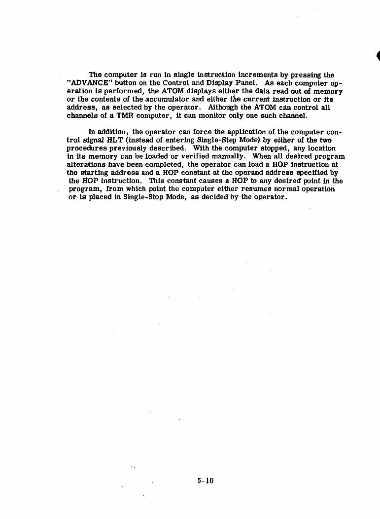
The computer is run in single instruction increments by pressing the"ADVANCE" button on the Control and Display Panel. As each computer op-eration is performed, the ATOM displays either the data read out of memoryor the contents of the accumulator and either the current instruction or itsaddress, as selected by the operator. Although the ATOM can control allchannels of a TMR computer, it can monitor only one such channel.
In addition, the operator can force the application of the computer con-trol signal HLT (instead of entering Single-Step Mode) by either of the twoprocedures previously described. With the computer stopped, any locationin its memory can be loaded or verified manually. When all desired programalterations have been completed, the operator can load a HOP instruction atthe starting address and a HOP constant at the operand address specified bythe HOP instruction. This constant causes a HOP to any desired point in theprogram, from which point the computer either resumes normal operationor is placed in Single-Stop Mode, as decided by the operator.
5-10