appendix a distributed capacitance - springer978-0-306-47038...appendix a: distributed capacitance...
TRANSCRIPT
Appendix ADistributed Capacitance
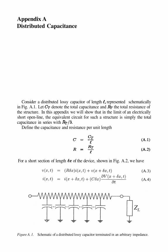
Consider a distributed lossy capacitor of length represented schematicallyin Fig. A.1. Let denote the total capacitance and the total resistance ofthe structure. In this appendix we will show that in the limit of an electricallyshort open-line, the equivalent circuit for such a structure is simply the totalcapacitance in series with
Define the capacitance and resistance per unit length
For a short section of length of the device, shown in Fig. A.2, we have
Figure A. 1. Schematic of a distributed lossy capacitor terminated in an arbitrary impedance.

168 INDUCTORS AND TRANSFORMERS FOR SI RF ICS
Figure A.2. A short segment of the distributed lossy capacitor.
Letting
For the time-harmonic case, we have the following set of coupled ordinarydifferential equations
The equations are decoupled by taking the derivative of the above equations
The above boundary value problem can be solved once the following boundaryconditions are imposed
where is the load impedance terminating the lossy capacitor. Consider theeigenfunction solution Since we require that

Appendix A: Distributed Capacitance 169
or
where so that
Note that the propagation and attenuation constant are equal,The general solution is thus
The unknown coefficients are found by imposing the boundary conditions. Theinput impedance is therefore
Consider the limit of a short line at zero frequency such that andThen we have as expected. Similarly, consider a shorted line suchthat Then
If we consider now the above in the limit of a short line, we have asexpected.
The limiting case of interest is that of an open line. Taking the limitwe have
Expanding the hyperbolic cotangent function in a Taylor series we have
This is what we set out to prove.

References
[Abramowitz and Stegun, 1972] Abramowitz, M. and Stegun, I. A. (1972).Handbook of Mathematical Functions with Formulas, Graphs, and Mathe-matical Tables. John Wiley and Sons, Inc., New York.
[Ashby et al., 1996] Ashby, K. B., Koullias, I. A., Finley, W. C., Bastek, J. J.,and Moinian, S. (1996). High q inductors for wireless applications in acomplementary silicon bipolar process. IEEE Journal of Solid-State Circuits,31:4–9.
[Ayasli et al., 1982] Ayasli, Y., Mozzi, R. L., Vorhaus, J, L., Reynolds, L. D.,and Pucel, R. A. (1982). A monolithic gaas 1-13 ghz traveling-wave ampli-fier. IEEETrans. Microwave Theory Tech., MTT-30:976–981.
[Beyer et al., 1984] Beyer, J. B., Prasad, S. N., Becker, R. C., Nordman, J. E.,and Hohenwarter, G. K. (1984). Mesfet distributed amplifier design guide-lines. IEEE Trans. Microwave Theory Tech., MTT-32:268–275.
[Boulouard and Le Rouzic, 1989] Boulouard, A. and Le Rouzic, M. (1989).Analysis of rectangular spiral transformers for mmic applications. IEEETransactions on Microwave Theory and Techniques, 37:1257–60.
[Burghartz et al., 1996a] Burghartz, J. N., Jenkins, K. A., and Soyuer, M.(1996a). Multilevel-spiral inductors using vlsi interconnect technology.IEEE Electron Device Letters, 17:428–30.
[Burghartz et al., 1997] Burghartz, J. N., Ruehli, A. E., Jenkins, K. A., Soyuer,M., and Nguyen-Ngoc, D. (1997). Novel substrate contact structure forhigh-q silicon-integrated spiral inductors. In International Electron DevicesMeeting, pages 55–8.

172 INDUCTORS AND TRANSFORMERS FOR SI RF ICS
[Burghartz et al., 1996b] Burghartz, J. N., Soyuer, M., and Jenkins, K. A.(1996b). Integrated rf and microwave components in bicmos technology.IEEE Transactions on Electron Devices, 43:1559–70.
[Burghartz et al., 1995] Burghartz, J. N., Soyuer, M., Jenkins, K. A., and Hul-vey, M. D. (1995). High-q inductors in standard silicon interconnect technol-ogy and its application to an integrated rf power amplifier. In InternationalElectron Devices Meeting, pages 1015–8.
[Cahana, 1983] Cahana, D. (1983). A new transmission line approach fordesigning spiral microstrip inductors for microwave integrated circuits. InIEEE MTT-S International Microwave Symposium Digest, pages 245–7.
[Carlin and Giordano, 1964] Carlin, H. J. and Giordano, A. B. (1964). Networktheory; an introduction to reciprocal and non-reciprocal circuits. Prentice-Hall, Englewood Cliffs, N.J.
[Chang et al., 1993] Chang, J. Y.-C, Abidi, A. A., and Gaitan, M. (1993).Large suspended inductors on silicon and their use in a 2 µm cmos rf ampli-fier. IEEE Electron Device Letters, 14:246–8.
[Collin, 1990] Collin, R. E. (1990). Field theory of guided waves. IEEE Press,New York, 2nd edition.
[Craninckx and Steyaert, 1995] Craninckx, J. and Steyaert, M. S. J. (1995). A1.8-ghz cmos low-phase-noise voltage-controlled oscillator with prescaler.IEEE Journal of Solid-State Circuits, 30:1474–82.
[Craninckx and Steyaert, 1997] Craninckx, J. and Steyaert, M. S. J. (1997). A1.8-ghz low-phase-noise cmos vco using optimized hollow spiral inductors.IEEE J. Solid-State Circuits, 32:736–744.
[Danesh et al., 1998] Danesh, M., Long, J. R., Hadaway, R. A., and Harame,D. L. (1998). A q-factor enhancement technique for mmic inductors. InIEEE MTT-S International Microwave Symposium Digest, pages 183–6.
[Dec and Suyama, 1997] Dec, A. and Suyama, K. (1997). Micromachinedvaractor with wide tuning range. Electronics Letters, 33:922–4.
[Dekker et al., 1997] Dekker, R., Baltus, P., van Deurzen, M., Einden, W.,Maas, H., and Wagemans, A. (1997). An ultra low-power rf bipolar tech-nology on glass. In International Electron Devices Meeting, pages 921–3.
[Demir et al., 1998] Demir, A., Mehrotra, A., and Roychowdhury, J. (1998).Phase noise in oscillators: a unifying theory and numerical methods forcharacterisation. In Design and Automation Conference, pages 26–31.

References 173
[Desoer and Kuh, 1969] Desoer, C. A. and Kuh, E. S. (1969). Basic circuittheory. McGraw-Hill, New York.
[Dongarra and Demmel, 1991] Dongarra, J. and Demmel, J. (1991). Lapack:a portable high-performance numerical library for linear algebra. Supercom-puter, 8:33–8.
[Erzgraber et al., 1998] Erzgraber, H. B., Grabolla, T., Richter, H. H., Schley,P., and Wolff, A. (1998). A novel buried oxide isolation for monolithicrf inductors on silicon. In International Electron Devices Meeting, pages535–9.
[et al., 1983] et al., R. P. (1983). Quadpack: A Subroutine Package for Auto-matic Integration. Springer-Verlag, Berlin; New York.
[Eynde et al., 2000] Eynde, F. O., Craninckx, J., and Goetschalckx, P. (2000).A fully-integrated zero-if dect transceiver. In IEEE International Solid-StateCircuits Conference, pages 138–9,450.
[Feynman et al., 1963] Feynman, R. P., Leighton, R. B., and Sands, M. L.(1963). The Feynman lectures on physics volume 2. Addison-Wesley Pub.Co, Reading, Mass.
[Frigo and Johnson, 1998] Frigo, M. and Johnson, S. G. (1998). Fftw: an adap-tive software architecture for the fft. In IEEE International Conference onAcoustics, Speech and Signal Processing, pages 1381–4.
[Geen et al., 1989] Geen, M. W., Green, G. J., Arnold, R. G., Jenkins, J. A.,and Jansen, R. H. (1989). Miniature multilayer spiral inductors for gaasmmics. In 11th Annual GaAs 1C Symposium, pages 303–6.
[Gharpurey and Meyer, 1995] Gharpurey, R. and Meyer, R. G. (1995). Analy-sis and simulation of substrate coupling in integrated circuits. InternationalJournal of Circuit Theory and Applications, 23:381–394.
[Gharpurey and Meyer, 1996] Gharpurey, R. and Meyer, R. G. (1996). Mod-eling and analysis of substrate coupling in integrated circuits. IEEE Journalof Solid-State Circuits, 31(3):344–53.
[Gray and Meyer, 1993] Gray, P. R. and Meyer, R. G. (1993). Analysis anddesign of analog integrated circuits. Wiley, New York, 3rd edition.
[Gray and Meyer, 1995] Gray, P. R. and Meyer, R. G. (1995). Future directionsin silicon ics for rf personal communications. In IEEE International Solid-State Circuits Conference, pages 83–90.

174 INDUCTORS AND TRANSFORMERS FOR SI RF ICS
[Greengard and Rokhlin, 1997] Greengard, L. and Rokhlin, V. (1997). Afast algorithm for particle simulations. Journal of Computational Physics,135:280–92.
[Greenhouse, 1974] Greenhouse, H. M. (1974). Design of planar rectangularmicroelectronic inductors. IEEE Trans. Parts, Hybrids and Packaging, PHP-10:101–9.
[Grover, 1946] Graver, F. W. (1946). Inductance Calculations. Van Nostrand,Princeton, N.J.
[Hajimiri and Lee, 1998] Hajimiri, A. and Lee, T. H. (1998). A general theoryof phase noise in electrical oscillators. IEEE Journal of Solid-State Circuits,33:179–94.
[Hasegawa et al., 1971] Hasegawa, H., Furukawa, M., and Yanai, H. (1971).Properties of microstrip line on system. IEEE Transactions on Mi-crowave Theory and Techniques, 11:869–81.
[Hejazi et al., 1998] Hejazi, Z., Excell, P., and Jiang, Z. (1998). Accurate dis-tributed inductance of spiral resonators. IEEE Microwave and Guided WaveLetters, 8:164–6.
[Huan-Shang et al., 1997] Huan-Shang, T., Lin, L. J., Frye, R. C., Tai, K. L.,Lau, M. Y., Kossives, D., Hrycenko, F., and Young-Kai, C. (1997). In-vestigation of current crowding effect on spiral inductors. In IEEE MTT-SInternational Microwave Symposium Digest, pages 139–142.
[Hurley and Duffy, 1995] Hurley, W. G. and Duffy, M. C. (1995). Calculationof self and mutual impedances in planar magnetic structures. IEEE Trans.Magnetics, 31:2416–22.
[Hurley and Duffy, 1997] Hurley, W. G. and Duffy, M. C. (1997). Calculationof self- and mutual impedances in planar sandwich inductors. IEEE Trans.Magnetics, 33:2282–90.
[Jackson, 1999] Jackson, J.D. (1999). Classical electrodynamics. Wiley, NewYork, 3rd edition.
[Jaeger, 1993] Jaeger, R. C. (1993). Introduction to microelectronic fabrica-tion. Addison-Wesley Pub. Co., Reading, Mass.
[Jansen et al., 1997] Jansen, S., Negus, K., and Lee, D. (1997). Silicon bipolarvco family for 1.1 to 2.2 ghz with fully-integrated tank and tuning circuits.In IEEE International Solid-State Circuits Conference, pages 392–93.

References 175
[Jiang et al., 1997] Jiang, Z., Excell, P. S., and Hejazi, Z. M. (1997). Calcula-tion of distributed capacitances of spiral resonators. IEEE Transactions onMicrowave Theory and Techniques, 45:139–42.
[Johns and Martin, 1997] Johns, D. and Martin, K. W. (1997). Analog inte-grated circuit design. Wiley, New York.
[Johnson et al., 1996] Johnson, R. A., Chang, C. E., Asbeck, P. M., Wood,M. E., Garcia, G. A., and Lagnado, I. (1996). Comparison of microwave in-ductors fabricated on silicon-on-sapphire and bulk silicon. IEEE Microwaveand Guided Wave Letters, 6:323–5.
[Kaertner, 1990] Kaertner, F. X. (1990). Analysis of white and noise inoscillators. Int. J. Circuit Theory Appl., 18:485–519.
[Kamogawa et al., 1999] Kamogawa, K., Nishikawa, K., Toyoda, I., Toku-mitsu, T., and Tanaka, M. (1999). A novel high-q and wide-frequency-rangeinductor using si 3-d mmic technology. IEEE Microwave and Guided WaveLetters, 9:16–18.
[Kamon et al., 1994a] Kamon, M., Ttsuk, M. J., and White, J. K. (1994a).Fasthenry: amultipole-accelerated 3-d inductance extraction program. IEEETransactions on Microwave Theory and Techniques, 42:1750–8.
[Kamon et al., 1994b] Kamon, M., Ttsuk, M. J., and White, J. K. (1994b).Fasthenry: a multipole-accelerated 3-d inductance extraction program. IEEETrans. Microwave Theory Tech., 42:1750–58.
[Kapur and Long, 1997] Kapur, S. and Long, D. E. (1997). Ies3: a fast inte-gral equation solver for efficient 3-dimensional extraction. In IEEE/ACMInternational Conference on Computer-Aided Design, pages 448–55.
[Kim et al., 1995] Kim, B.-K.,Ko,B.-K.,Lee, K., Jeong, J.-W., Lee,K.-S.,andKim, S.-C. (1995). Monolithic planar rf inductor and waveguide structures onsilicon with performance comparable to those in gaas mmic. In InternationalElectron Devices Meeting, pages 717–20.
[Kim and O, 1997] Kim, K. and O, K. (1997). Characteristics of an integratedspiral inductor with an underlying n-well. IEEE Transactions on ElectronDevices, 44:1565–7.
[Kittel, 1996] Kittel, C. (1996). Introduction to solid state physics. Wiley,New York, 7th edition.
[Kouznets and Meyer, ] Kouznets, K. and Meyer, R. G. Phase noise in 1c os-cillators, submitted for publication.
176 INDUCTORS AND TRANSFORMERS FOR SI RF ICS
[Krafcsik and Dawson, 1986] Krafcsik, D. M. and Dawson, D. E. (1986). Aclosed-form expression for representing the distributed nature of the spiralinductor. In IEEE Microwave and Millimeter-Wave Monolithic CircuitsSymposium. Digest of Papers, pages 87–92.
[Kuhn et al., 1995] Kuhn, W. B., Elshabini-Riad, A., and Stephenson, F. W.(1995). Centre-tapped spiral inductors for monolithic bandpass filters. Elec-tronics Letters, 31:625–6.
[Lee et al., 1998a] Lee, J., Karl, A., Abidi, A. A., and Alexopoulos, N. G.(1998a). Design of spiral inductors on silicon substrates with a fast simulator.In European Solid-State Integrated Circuits Conference.
[Lee et al., 1998b] Lee, Y.-G., Yun, S.-K., and Lee, H.-Y. (1998b). Novel high-q bondwire inductor for mmic. In International Electron Devices Meeting,pages 548–51.
[Leeson, 1966] Leeson, D. B. (1966). A simple model for oscillator noisespectrum. Proc. IEEE, 54:329–330.
[Long and Copeland, 1997] Long, J. R. and Copeland, M. A. (1997). Themodeling, characterization, and design of monolithic inductors for silicon ific’s. IEEE J. Solid-State Circuits, 32:357–69.
[Long et al., 1996] Long, J. R., Copeland, M. A., Kovacic, S. J., Malhi, D. S.,and Harame, D. L. (1996). Rf analog and digital circuits in sige technology.In IEEE International Solid-State Circuits Conference, pages 82–83.
[Lopez-Villegas et al., 2000] Lopez-Villegas, J. M., Samitier, J., Cane, C,Losantos, P., and Bausells, J. (2000). Improvement of the quality factorof rf integrated inductors by layout optimization. IEEE Transactions onMicrowave Theory and Techniques, 48:76–83.
[Lovelace et al., 1994] Lovelace, D., Camilleri, N., and Kannell, G. (1994).Silicon mmic inductor modeling for high volume, low cost applications.Microwave Journal, 37:60–71.
[Mahmoud and Beyne, 1997] Mahmoud, S. F. and Beyne, E. (1997). Induc-tance and quality-factor evaluation of planar lumped inductors in a multilayerconfiguration. IEEE Trans. Microwave Theory Tech., 45:918–23.
[Merrill et al., 1995] Merrill, R. B., Lee, T. W., You, H., Rasmussen, R., andMoberly, L. A. (1995). Optimization of high q integrated inductors formulti-level metal cmos. In International Electron Devices Meeting, pages983–6.

References 177
[Meyer et al., 1997] Meyer, R. G., Mack, W. D., and Hageraats, J. J. E. M.(1997). A 2.5-ghz bicmos transceiver for wireless lans. IEEE Journal ofSolid-State Circuits, 12:2097–104.
[Mohan et al., 1999] Mohan, S. S., del Mar Hershenson, M., Boyd, S. P., andLee, T. H. (1999). Simple accurate expressions for planar spiral inductances.IEEE Journal of Solid-State Circuits, 34:1419–24.
[Mohan et al., 1998] Mohan, S. S., Yue, C. P., del Mar Hershenson, M., Wong,S. S., and Lee, T. H. (1998). Modeling and characterization of on-chiptransformers. In International Electron Devices Meeting, pages 531–4.
[Muller and Kamins, 1986] Muller, R. S. and Kamins, T. I. (1986). Deviceelectronics for integrated circuits. Wiley, New York, 2nd edition.
[Nabors and White, 1991] Nabors, K. and White, J. K. (1991). Fastcap: a mul-tipole accelerated 3-d capacitance extraction program. IEEE Transactionson Computer-Aided Design of Integrated Circuits and Systems, 10:1447–59.
[Neudeck, 1983] Neudeck, G. W. (1983). The bipolar junction transistor.Addison-Wesley, Reading, Mass.
[Neudeck, 1989] Neudeck, G. W. (1989). The PN junction diode. Addison-Wesley, Reading, Mass., 2nd edition.
[Nguyen and Meyer, 1990] Nguyen, N. M. and Meyer, R. G. (1990). Si ic-compatible inductors and 1c passive filters. IEEE J. Solid-State Circuits,27:1028–31.
[Niknejad, ] Niknejad, A. M. Discussion during ieee 1997 custom integratedcircuits conference author interview.
[Niknejad, 1997] Niknejad, A. M. (1997). Analysis, design, and optimizationof spiral inductors and transformers for si fr ics: research project. Master’sthesis, University of California, Berkeley.
[Niknejad et al., 1998] Niknejad, A. M., Gharpurey, R., and Meyer, R. G.(1998). Numerically stable green function for modeling and analysis ofsubstrate coupling in integrated circuits. IEEE Trans. CAD, 17:305–315.
[Niknejad and Meyer, ] Niknejad, A. M. and Meyer, R. G. Asitic: Analysis of siinductors and transformers for ics. http://www.eecs.berkeley.edu/~niknejad.
[Niknejad and Meyer, 1997] Niknejad, A. M. and Meyer, R. G. (1997). Anal-ysis and optimization of monolithic inductors and transformers for rf ics. InIEEE International Solid-State Circuits Conference, pages 375–8.

178 INDUCTORS AND TRANSFORMERS FOR SI RF ICS
[Niknejad and Meyer, 1998] Niknejad, A. M. and Meyer, R. G. (1998). Anal-ysis, design, and optimization of spiral inductors and transformers for si ifics. IEEE J. Solid-State Circuits, 33:1470–81.
[Park et al., 1997a] Park, M., Kim, C. S., Park, J. M., Yu, H. K., and Nam, K. S.(1997a). High q microwave inductors in cmos double-metal technology andits substrate bias effects for 2 ghz if ics application. In International ElectronDevices Meeting, pages 59–62.
[Park et al., 1997b] Park, M., Lee, S., Yu, H. K., Koo, J. G., and Nam, K. S.(1997b). High q cmos-compatible microwave inductors using double-metalinterconnection silicon technology. IEEE Microwave and Guided WaveLetters, 7:45–7.
[Percival, 1937] Percival, W. S. (1937). British Patent 460562.
[Pettenpaul and et al., 1988] Pettenpaul, E. and et al., H.K. (1988). Cadmodelsof lumped elements on gaas up to 18 ghz. IEEE Trans. Microwave TheoryTech., 36:294–304.
[Pierret, 1990] Pierret, R.F. (1990). Field effect devices. Addison-Wesley Pub.Co., Reading, Mass., 2nd ed edition.
[Poritsky and Jerrard, 1954] Poritsky, H. and Jerrard, R. P. (1954). Eddy-current losses in a semi-infinite solid due to a nearby alternating current.Trans. Am. Inst. Elect. Engrs, part I, 73:97–106.
[Pozar, 1997] Pozar, D. M. (1997). Microwave Egineering. Wiley, New York,NY, 2nd edition.
[Proakis, 1995] Proakis, J. G. (1995). Digital communications. McGraw-Hill,New York, 3rd edition.
[Rabjohn, 1991] Rabjohn, G. G. (1991). Monolithic microwave transformers.Master’s thesis, Carleton University.
[Ramo et al., 1994] Ramo, S., Whinnery, J. R., and Duzer, T. V. (1994). Fieldsand Waves in Communication Electronics. John Wiley and Sons, Inc., NewYork, 3rd ed. edition.
[Rategh and Lee, 1999] Rategh, H. R. and Lee, T. H. (1999). Superharmonicinjection-locked frequency dividers. IEEE Journal of Solid-State Circuits,34:813–21.
[Rautio, 1999] Rautio, J. C. (1999). Free em software analyzes spiral inductoron silicon. Microwaves and RF, pages 165–9.
References 179
[Razavi, 1998] Razavi, B. (1998). RF microelectronics. Prentice Hall, UpperSaddle River, NJ.
[Rejaei et al., 1998] Rejaei, B., Tauritz, J. L., and Snoeij, P. (1998). A predictivemodel for si-based circular spiral inductors. In IEEE MTT-S InternationalMicrowave Symposium Digest, pages 148–54.
[Roach, 1982] Roach, G. F. (1982). Green’s Functions. Cambridge UniversityPress, Cambridge; New York, 2nd edition.
[Rofougaran et al., 1998a] Rofougaran, A., Chang, G., Rael, J. J., Chang, J.Y.-C, Rofougaran, M., Chang, P., Djafari, M., Ku, M.-K., Roth, E., Abidi,A., and Samueli, H. (April 1998a). A single-chip 900-mhz spread-spectrumwireless transceiver in 1- c mos. i. architecture and transmitter design.IEEE Journal of Solid-State Circuits, 33(4):515–34.
[Rofougaran et al., 1998b] Rofougaran, A., Chang, G., Rael, J. J., Chang, J.Y.-C., Rofougaran, M., Chang, P., Djafari, M., Min, J., Roth, E., Abidi, A.,and Samueli, H. (April 1998b). A single-chip 900-mhz spread-spectrumwireless transceiver in 1- cmos. ii. receiver design. IEEE Journal ofSolid-State Circuits, 33(4):535–47.
[Rudell et al., 1997] Rudell, J., Ou, J.-J., Cho, T., Chien, G., Brianti, F., Wel-don, J., and Gray, P. R. (1997). A 1.9 ghz wide-band if double conversioncmos integrated receiver for cordless telephone applications. In IEEE Inter-national Solid-State Circuits Conference, pages 304–5, 476.
[Ruehli, 1974] Ruehli, A. (1974). Equivalent circuit models for three-dimensional multiconductor systems. IEEE Transactions on MicrowaveTheory and Techniques, MTT-22:216–21.
[Ruehli, 1972] Ruehli, A. E. (1972). Inductance calculations in a complexintegrated circuit environment. IBM J. Res. Develop., 16:470–481.
[Ruehli and Heeb, 1992] Ruehli, A. E. and Heeb, H.(1992). Circuit models forthree-dimensional geometries including dielectrics. IEEE Trans. MicrowaveTheory Tech, 40:1507–1516.
[Ruehli et al., 1995] Ruehli, A. E., Miekkala, U., and Heeb, H. (1995). Stabilityof discretized partial element equivalent efie circuit models. IEEE Trans.Antennas Propag., 43:553–9.
[Samori et al., 1998] Samori, C., Lacaita, A. L., Villa, F., and Zappa, F. (1998).Spectrum folding and phase noise in 1c tuned oscillators. IEEE Trans. Cir-cuits Syst. II, Analog Digit. Signal Process, 45:781–90.
180 INDUCTORS AND TRANSFORMERS FOR SI RF ICS
[Schmuckle, 1993] Schmuckle, F. J. (1993). The method of lines for the anal-ysis of rectangular spiral inductors (in mmics). IEEE Transactions on Mi-crowave Theory and Techniques, 41:1183–6.
[Shepherd, 1986] Shepherd, P. R. (1986). Analysis of square-spiral inductorsfor use in mmic’s. IEEE Trans. on MTT, MTT-34:467–472.
[Soyuer et al., 1995] Soyuer, M., Burghartz, J. N., Jenkins, K. A., Ponnapalli,S., Ewen, J. R, and Pence, W. E. (1995). Multilevel monolithic inductors insilicon technology. Electronics Letters, 31:359–60.
[Steyaert et al., 1998] Steyaert, M., Borremans, M., Janssens, J., de Muer, B.,Itoh, I., Craninckx, J., Crols, J., Morifuji, E., Momose, S., and Sansen, W.(1998). A single-chip cmos transceiver for dcs-1800 wireless communica-tions. In IEEE International Solid-State Circuits Conference, pages 48–9,411.
[Stoll, 1974] Stoll, R. L. (1974). The Analysis of Eddy Currents. ClarendonPress, Oxford.
[Tegopoulos and Kriezis, 1985] Tegopoulos, J. A. and Kriezis, E. E. (1985).Eddy Currents in Linear Conducting Media. Elsevier Science Pub. Co.,Amsterdam; New York: Elsevier; New York: Distributors for the U.S. andCanada.
[Trim, 1990] Trim, D. W. (1990). Applied Partial Differential Equations.PWS-KENT, Boston.
[Vendelin and A. M. Pavio, 1990] Vendelin, G. D. and A. M. Pavio, U. L. R.(1990). Microwave Circuit Design Using Linear and Nonlinear Techniques.Wiley, New York, NY.
[Wait, 1982] Wait, J.R.(1982). Geo-electromagnetism. Academic Press, NewYork.
[Weeks et al., 1979] Weeks, W. T., Wu, L. L., McAllister, M. F., and Singh, A.(1979). Resistive and inductive skin effect in rectangular conductors. IBMJ. Res. Develop., 23:652–660.
[Wolfram, 1999] Wolfram, S. (1999). The Mathematica Book. Wolfram Me-dia; Cambridge University Press, Champaign, IL; New York, 4th edition.
[Yoon et al., 1998] Yoon, J.-B., Kim, B.-K., Han, C.-H., Yoon, E., Lee, K.,and Kim, C.-K. (1998). High-performance electroplated solenoid-type in-tegrated inductor for rf applications using simple 3d surface microma-chining technology. In International Electron Devices Meeting.

References 181
[Yoshitomi et al., 9998] Yoshitomi, T., Sugawara, Y., Morifuji, E., Ohguro, T.,Kimijima, H., Morimoto, T., Momose, H. S., Katsumata, Y, and Iwai, H.(19998). On-chip spiral inductors with diffused shields using channel-stopimplant. In International Electron Devices Meeting, pages 540–3.
[Young and Boser, 1197] Young, D. J. and Boser, B. E. (1197). Amicromachine-based rf low-noise voltage-controlled oscillator. In IEEEInternational Solid-State Circuits Conference, pages 431–4.
[Young et al., 1997] Young, D. J., Malba, V., Ou, J.-J., Bernhardt, A. E, andBoser, B. E. (1997). A low-noise rf voltage-controlled oscillator using on-chip high-q three-dimensional coil inductor and micromachined variablecapacitor. In International Electron Devices Meeting, pages 128–31.
[Yue and Wong, 1997] Yue, C. and Wong, S. (1997). On-chip spiral inductorswith patterned ground shields for si-based rf ic’s. In IEEE Symposium onVLSI Circuits, pages 85–6.
[Yue and Wong, 1998] Yue, C. P. and Wong, S. S. (1998). On-chip spiral in-ductors with patterned ground shields for si-based rf ic’s. IEEE Journal ofSolid-State Circuits, 13:743–52.
[Zannoth et al., 1998] Zannoth, M., Kolb, B., Fenk, J., and Weigel, R. (1998).A fully integrated vco at 2 ghz. In IEEE International Solid-State CircuitsConference, pages 224–5.
[Zhou, 1993] Zhou, P.-b. (1993). Numerical analysis of electromagnetic fields.Springer-Verlag, Berlin ; New York.

Index
AS1TIC, 97–107capacitors, 133geometry engine, 99library dependence, 99numerical calculations, 100–101organization, 99–100technology file, 99visualization, 106–107
ABCD matrix, 150active area, 134active device
typical examples, 12aluminum, 16, 17, 88
sheet resistance, 17spiking, 17thickness, 17
analysiscapacitors, 103transformers, 103–106two-port, 102–103
anisotropy, 46antenna, 6, 15
efficiency, 126applications
artificial transmission line, 5, see dis-tributed amplifier
balun, 5center-tapped transformer, 5differential operation, 5distributed amplifier, 5filters, 5impedance matching, 4LC tuned load, 5low noise amplifier, 4, 7mixer, 4phase locked loops, 7power amplifier, 4series-feedback, 5tank, 7
traveling-wave amplifier, 5voltage controlled oscillator, 7wireless transceiver, 6
arithmetic mean distance (AMD), 68attenuation constant, 150, 159, 160, 169avalanche
breakdown, 32multiplication, 36
balun, 28base-pinch, 34basis function
spatially localized, 54battery life, 8Bessel function, 93bias voltage, 141BiCMOS, 8–9, 20, 21, 34, 75, 109, 128bipolar, 20, 21, 34, 75, 109, 128, 139bisected- π m-derived section, 155black-box, 11BLAS, 99, 100bond
pad, 29, 35pad capacitance, 111wire, 21, 26, 42
bottom plate, 134boundary conditions, 21, 50, 54, 79, 80, 83, 103,
168, 169boundary method, 52breakdown, 32broadband, 5, 149bulk substrate, 21, 75buried oxide isolation, 42bypass, 132
calibration, 110capacitance, 59
pn-junction, 33linear, 132–133matrix, 57, 59, 104

184 INDUCTORS AND TRANSFORMERS FOR SI RF ICS
tolerance, 35capacitive
coupling, 28, 102current injection, 129
capacitor, 34–35distributed, 167–169metal-metal, 34, 133–134, 141MOS, 33–34, 133poly-poly metal, 34
cellular communication, 6center-tap, 22center-tapped
inductor, 129transformers, 28
channel length, 158charge and current discretization, 53charge conservation, 100chemical vapor deposition, 20circular, 22circular symmetry, 43, 81CMOS, 8–9, 16, 17, 20, 21, 34, 42, 75, 109, 112,
128, 152, 160co-planar probes, 110coil, 22, 39, 41Colpitts oscillator, 140common ground, 103common mode rejection, 135complex power, 60conduction current, 31conductive
losses, 48substrate, 18–21
conservation of energy, 13constitutive relations, 45constructive interference, 150copper, 17, 88coupled inductors, 109coupled transmission lines, 40, 129, 149coupling factor, 28current constriction, 27, 43, 72, 106current crowding, 17–18, 43current density plot, 73, 100current distribution, 17
high frequency, 68cutoff frequency, 151, 159, 160
depletion, 33depletion mode, 34depletion region, 31
thickness, 32, 34device layout, 21–31diamagnetic, 19, 46, 76die photo, 144dielectric
effective, 49dielectric constant, 40dielectric losses, 152
differential, 5circuits, 22operation, 129quad, 141quality factor, 129structure, 134
diffusion, 20current, 31length, 32process, 9resistor, 34
digitalhigh speed, 17, 59, 163, 164integration, 8interconnect, 164market growth, 9noise, 8, 36, 164
digital signal processing, 7, 8diode, 12, 31–33, 133Dirac delta function, 51direct conversion, 7discrete components, 6discrete cosine transform, 100discretization
charge, 55current, 54
displacement current, 18, 32, 35, 53, 65, 88, 90,104
dissipation matrix, 12distributed amplifier
actively loaded line, 160–161artificial transmission line, 150design tradeoffs, 158–160gain, 156–158introduction, 149–150number of stages, 150optimal number of stages, 159–160
distributed effects, 40distributed resistance, 34divider, 134
current consumption, 143headroom, 143latch based, 143speed, 143
domain techniques, 52doping, 141
profile, 52down-bonds, 21down-conversion, 146drain, 36
line, 5, 149, 155line impedance, 159lossy line, 151
dynamic range, 5, 8
eddy currents, 9, 21, 26, 29, 41, 43, 72, 76, 77,80, 81, 102, 109, 113, 122, 152
3-d solution, 81–84
Index 185
boundary value problem, 78–81circular symmetry, 81combating, 26equation, 50generated by square spirals, 92–93high frequency, 88–92losses, 75, 91low frequency, 84–88single substrate layer, 93substrate, 18two layer substrate , 94
efficiency, 5, 8eigenfunction, 54electric
center, 23energy storage, 32force, 69response, 76
electrically short open-line, 167electromigration, 17EM simulation, 42emitter
coupled logic, 134follower, 134, 143
energy storage, 11, 14entropy, 15epitaxial growth, 109epitaxial layer, 21epitaxial pinch, 34epitaxy, 20epoxy, 21equivalent
resistance, 85equivalent circuit, 129
near resonance, 119shielded MIM capacitors, 133
external components, 5
Faraday’s law, 60, 62, 69FASTHENRY, 89feedback
factor, 134network, 141
ferromagnetic, 46FET
losses, 151model, 153, 156
FFTW, 99filament, 39filters
channel selection, 126gm-C, 5MOSFET-C, 5, 34surface acoustic wave, 5
finite difference equation, 52finite difference time domain, 43finite element method, 52
flicker noise, 138–140free-space, 50, 80, 90
kernel, 89frequency division, 127, 142–143frequency division multiplexing, 126frequency hopped multiple access, 126
G-S-G probes, 111–113GaAs, 8–9, 18, 40, 48gain compression, 31gain-bandwidth product, 149gate
line, 5, 149, 155line impedance, 159lossy line, 151oxide, 33resistance, 158
gaugeCoulomb, 46, 76, 78Lorenz, 46, 48lossy media, 48
geometriccenter, 23
gold, 17, 40, 88Green function, 43, 50–53, 87, 88, 100, 101, 103,
106averaged, 65circular, 43dyadic, 51–52, 63electric, 53free-space, 43, 75full-wave, 43magnetic, 54
Green’s identities, 51, 52Greenhouse, 39, 40, 42ground, 21, 111
back-plane, 18, 21, 35bounce, 31conductors, 102inductance, 31on-chip, 21plane, 68secondary, 104structure, 29substrate, 41
Grover, 39, 42gyrator, 14
half-wavelength, 129heat, 15, 17, 18, 128Helmholtz
equations, 52theorem, 47
Hermitian matrix, 13high quality factor, 7high-field region, 36hollow spiral, 27, 43hot electron effects, 36

186 INDUCTORS AND TRANSFORMERS FOR SI RF ICS
Hypergeometric function, 93hysteresis, 46
imagecurrents, 20, 29, 40, 83, 85, 91, 113impedance, 153impedance matching, 155parameter method, 150
lossless transmission line, 151lossy transmission line, 151–153
impedancematch, 4, 5, 17
impulse response function, 51incident power, 12induced
electric field, 60magnetic losses, 75substrate currents, 18
inductancebond wire, 4calculation
conductors, 67filamental, 66–67geometric mean distance, 39, 67–68,
90high frequency, 68–72hybrid method, 91parallel connection, 65–66series connection, 65
curve-fit, 43definition, 60–65
energy, 60–61magnetic flux, 61–62magnetic vector potential, 62–65
external, 70frequency-independent, 83high frequency, 68–72internal, 60lead frame, 4low frequency, 64mutual, 62, 63, 66, 90reflected, 83, 102self, 17, 62, 75simulated, 4tolerance, 26, 42
inductorlayout
non-planar, 24–26planar, 22–24
losses, 151multi-layer, 44polygon spiral, 109series connected, 41, 44shunt connected, 41stacked, 44
injection lock, 142inner turns of spiral, 72
instability, 31, 36integral operator
kernel, 87integrated circuit, 15, 17, 24, 31, 55, 59
cross-section of metal layers, 16–18radio frequency, 21technology, 8
interconnect, 17, 35intermediate frequency, 125, 126interwinding capacitance, 20, 26, 119inverse cosine transform, 80inversion, 34ion implantation, 20irreversible process, 15irrotational, 47isolation, 31, 113, 132iterative solution, 89
jamming, 31
k-factor, 28Kirchhoff’s current law, 56, 89, 100, 102Kirchhoff’s voltage law, 100, 102, 136Krylov sub-space iteration, 43
LAPACK, 99, 100latch, 143latch-up, 21, 109lateral
coil, 26, 41magnetic fields, 26
Leeson formula, 128Lenz’s law, 60, 85linear superposition, 51linearity, 5, 12, 46, 76, 87LINPACK, 99lithographic technology, 9local oscillator, 126, 142, 146logarithmic singularity, 83loop
gain, 138, 140inductor, 39
Lorentzian distribution, 15loss tangent, 48, 78, 103lossy capacitor, 30
m-derived matching network, 159magnetic
coupling, 102, 134energy, 60flux, 61force, 69monopole, 59mutual coupling, 22, 25response, 76vector potential, 62–63, 67
majority carriers, 33Manhattan geometry, 42

Index 187
manufacturabilitynon-planar structure, 119
master-slave, 143matching, 141, 143material properties, 15matrix compression, 102matrix-fill
capacitance, 100inductance, 101operation, 100–101
Maxwell, 39Maxwell’s equations, 39, 57, 76, 87, 88
discretization, 53–57inversion, 50–52numerical solution, 52–57time-period, 45
measurement, 109–122s-parameters, 113, 119device layout, 110eddy currents, 116effective inductance, 113effective series resistance, 113multi–layer structure, 119–122negative resistance, 116quality factor, 116, 120self-resonant frequency, 116, 119setup and calibration, 110–113single layer structure, 113–116
metallayers, 16losses, 16–18, 27, 40
eddy currents, 17–18ohmic, 17
pitch, 28spacing, 21, 27, 70, 72
method of moments, 43, 53micro-machined solenoid inductors, 42microstrip, 150minority carriers, 32, 34mixed-signal ICs, 36mixer, 125, 126, 142mode-locking, 31modulation, 126MOS,9multi-conductor system, 18multi-layer
inductorseries-connected, 110
spiralsseries-connected, 103shunt-connected, 103
substrate, 76multi-level metallization, 41
natural frequency, 13negative feedback, 31negative resistance, 13, 134, 160
Neumann’s equation, 64NMOS, 8noise, 5
control line, 131immunity, 134injection, 5power spectral density, 138up-conversion, 140
non-linear, 5, 12, 46non-uniform
currentdistribution, 27, 43, 72, 75, 91, 106media, 52
numerical integration, 54, 101magnetic vector potential, 90–92
numerical solutionassumptions, 53current flow, 88
off-chip, 5, 6, 31ohmic losses, 75, 103on-chip, 5, 6, 31, 60
filter, 142OpenGL, 100optimization, 72, 155optimum bias current, 141orthonormal set, 54oscillation amplitude, 130output buffers, 143oxide, 17, 20, 103
thickness, 33, 34, 119, 133
package, 4, 8, 21paddle, 21
palladium, 17panels
constant charge, 101paramagnetic, 46parametric amplifier, 12parasitic
coupling, 8, 31magnetic coupling, 129
partialinductance, 69inductance matrix, 25, 42, 54, 57, 65, 70,
89, 102reduction, 89
passivearea, 134network, 13
passive deviceapplications, 4–8definition, 11–13high power, 17metal losses, 16–18on-board, 3on-chip, 3quality factor, 14–15reciprocity, 13–14

188 INDUCTORS AND TRANSFORMERS FOR SI RF ICS
stability, 13substrate coupling, 36substrate losses, 18–19typical examples, 11
passivity, 13PEEC, 39, 43, 57, 75, 88, 90, 100–106penetration depth, 17, 21perfectly coupled inductors, 26phase
noise, 7, 126, 127, 142, 146velocity, 150, 157
planar metallization, 21planar structure, 120planarization constraints, 20platinum, 17pn junction
abrupt, 32barrier, 32built-in field, 32forward biased, 32, 109, 130leakage currents, 32linearly graded, 33reverse biased, 31, 32, 34, 41, 129, 141reverse-based, 36space-charge region, 32
Poisson’s equation, 51, 53, 55, 60, 78modified, 49vector form, 62
polygon, 22polyimide, 20, 41polysilicon, 16, 28, 41, 42positive definite matrix, 13positive feedback, 31, 134post-processing, 21potential
electric scalar, 46–47electromagnetic, 48magnetic vector, 46–47
poweramplifier, 5, 127delivered to one-port, 14dissipation, 14gain, 12injection, 5
Poynting’s theorem, 48, 84previous work
early research, 39GaAs substrate, 40Si substrate, 40–44
process parameters, 110, 119process variation, 141propagation
constant, 150–151, 153, 169mode, 19modeg, 19velocity, 157
proximity, 16, 20, 29
effect, 17–18, 27, 42, 75, 103, 152punctured matrix, 104
QUADPACK, 99, 101quality factor, 14–15, 25, 26, 29, 33, 34, 44, 126
capacitor, 122high frequency, 26, 127, 129metal losses, 16–18substrate losses, 18–19
quarter-wavelength, 129quasi-static, 76
radiation, 18, 47, 127, 128radio frequency, 29reactance
capacitive, 14frequency variation, 60inductive, 14
reactive energy, 16reciprocal mixing, 127reciprocity, 13–14, 64recursive-SVD
algorithm, 43reflected power, 12reflection coefficient, 13resistance
effective, 167high frequency, 18, 68, 70–72
resistivity, 21resistor, 7, 34–35
MOS, 34polysilicon, 34well, 34
reversible process, 15ring inductor, 39rotational
invariance, 81symmetry, 43
Ruehli, 39
S-G probes, 111–113scattering matrix, 12
symmetric, 13selective etching, 18, 40self
adjoint, 54resonance, 26
interwinding capacitance, 119substrate capacitance, 119
resonant frequency, 9, 17, 20, 27, 30–31,40, 41, 129
measured, 113separation of variables, 78, 82series connection, 24series to parallel transformation, 30shield, 28–31, 41, 113, 122, 133
currents, 29shallow junction diffused, 42

Index 189
short-channel MOS transistor, 36shot noise, 134shunt connection, 24Si, 8–9, 18, 19, 21, 46, 48, 76, 133
compatible inductors, 40intrinsic, 20, 41substrate resistivity, 18
SiGe, 8–9signal-to-noise ratio, 36single-ended, 5, 129singular value decomposition, 90skin depth, 21, 59, 101skin effect, 17–18, 27, 39, 42, 72, 75, 103, 113,
152bulk, 78
sliver, 17SNR, 31, 127solenoidal, 18, 47, 62, 64solver
iterative, 100SONNET, 44space-charge, 31spanning set, 54spectral leakage, 7, 31, 127SpectreRF, 136, 139, 143spiral, 22, 39
inductor, 18spurs, 31square, 22stability, 13, 160
conditional, 13staggered inductors, 41steady-state oscillation, 138stochastic bandpass signal, 126Stoke’s theorem, 62stratified substrate, 20, 55substrate, 8
conductive, 21, 128conductivity, 20contact, 35
halo, 31, 41coupling, 29, 31, 35–36, 111, 134current injection, 35currents, 91discretization, 53epi, 9, 43, 128, 152heavily resistive, 40high resistivity, 41induced losses, 21injection, 133insulating, 8, 18, 41, 152isolation, 31layers, 20loss matrix
algorithm, 93losses, 9, 18–19, 26, 27, 48, 53, 88
calculation of, 48–50
curtailing, 129electrically induced, 102, 103magnetically induced, 103
profile, 20–21bipolar, 20–21CMOS, 20–21
removal, 18thickness, 21
superheterodyne receiver, 7, 126surface waves, 19swing, 141symmetric inductors, 22
T-coils, 160T-section, 151, 152
center, 157tank
loading, 31quality factor, 128, 139
tapered spirals, 27, 43Taylor series, 169temperature variation, 141thermal noise, 134thermionic emission, 20thick metal, 17thick oxide, 17, 20, 40three-port model, 129time-varying, 12, 131, 139
magnetic field, 18, 27noise, 134transfer function, 136
titanium, 17tolerance
capacitance, 133top-metal, 17toroid, 22, 39transceiver
architecture, 7superheterodyne, 125
transformer, 18, 28, 43, 134k-factor, 28capacitive, 134center tap, 28metal-metal, 28non-planar, 109planar, 23, 109primary, 28, 103, 104secondary, 28, 103, 104turns ratio, 28
transistor, 12parasitics, 149
transmission coefficient, 13tungsten, 17tuning range, 33tunneling, 32twin-well, 21two-port parameters, 101

190 INDUCTORS AND TRANSFORMERS FOR SI RF ICS
uniformconvergence, 54current distribution, 42elements, 53
vacuum tube, 12varactor, 31–33, 129, 146
high frequency, 130losses, 129–132quality factor, 33, 34, 141resonance, 132
vertical coil, 26via, 23, 26, 55, 113virtual ground, 134, 135voltage controlled oscillator, 4, 33, 142, 146
die photo, 144differential, 129differential q-factor, 129effective capacitance, 137implementation, 141–142inductor design, 128–129introduction, 125–127measurement, 144–146
motivation, 127phase noise, 134–140simulation, 139test setup, 145–146topology, 134total capacitance, 137tuning range, 133varactor losses, 129–132
voltage headroom, 5
waveattenuation, 150propagation, 5, 18
wavelength, 19weak inversion, 33, 34well, 21winding capacitance, 113wireless communication, 17wireless LAN, 127
y-parameters, 110
zero IF, 7