appendix a using hdls for protocol aware ate1 - springer978-1-4419-7548-5/1.pdf · appendix a using...
TRANSCRIPT

393
Appendix AUsing HDLs for Protocol Aware ATE1
This Appendix describes the issues involved in transitioning from a design simulation environment to a physical test environment, especially in the case of complex (multicore) SOC devices. The article also discusses the advantages of using HDL code directly for programming of the tester hardware, as opposed to the traditional, bit-level language used in the past. In this case, the ability to be able to directly interpret and execute the HDL commands on the tester hardware is referred to as having “Protocol Aware” (PA) [1] capability. As the name suggests, this implies that the tester hardware has the ability, via reconfigurable firmware, to understand and execute high-level com-mands on physical hardware in the DUT’s native “Protocol” language. “Protocol Aware” is a larger umbrella that not only allows the tests to be constructed in an HDL format, but is also able to trans-late that into physical bits on test hardware.
A.1 Motivation
Modern semiconductor devices often behave in a nondeterministic manner not only in their end application but during test execution on ATE as well. This is the result of design methodologies that allow the assembly of the device from a library of IP blocks. These IP blocks often support specific industry standard protocols such as JTAG, DDR memory buses, PCI Express, etc. While the opera-tion of any individual block may be predictable, the relationship between the timing of protocols is often not. Today’s SOC ATE does not deal well with ambiguity. Any deviation from expected device behavior will cause that device to fail the ATE test, both during engineering development or produc-tion. Functionally testing devices that exhibit nondeterministic behavior is extremely difficult on current generation ATE.
A.2 Protocol Aware ATE
To deal with DUT nondeterministic behaviors, as part of the next round of UltraFLEX digital instru-ments Teradyne is developing a new ATE architecture – Protocol Aware ATE (PA). This project will require new software, hardware, and firmware. The intelligence required to handle protocols is contained in a FPGA on the ATE Pin Electronics instrument that can be reprogrammed based on the particular protocols required by any individual device program.
1 This text is taken from a paper by Eric Larson, Teradyne 2008 with his permission. The original paper can be down-loaded from the publisher’s site for this book, or by contacting Teradyne for this and other related materials.
Z. Navabi, Digital System Test and Testable Design: Using HDL Models and Architectures,DOI 10.1007/978-1-4419-7548-5, © Springer Science+Business Media, LLC 2011

394 Using HDLs for Protocol Aware ATE1
The list of potential protocols to support is endless and clearly they cannot be supported at once. Some are so low in volume that it may not be worth the effort. Others may be too complex to imple-ment in a practical manner. The hardware and software implementation of PA must be flexible enough to provide a solution for many different protocols. Some of these protocols have similar characteristics and can be thought of as a Protocol Family. Below is a partial list of popular proto-cols and potential groupings.
Low speed serial and parallel:
JTAG•MDIO•SRAM•Flash•
DRAM:
DDR, DDR2, DDR3•LPDDR, LPDDR2•GDDR3, GDDR4, GDDR5•
High speed serial:
PCI Express•SATA•DigRF•Serial RapidIO•
A.3 Protocol Aware ATE Implementation
While Protocol Aware ATE requires a new architecture and cannot be simply dropped into to exist-ing instruments it does offer the potential to increase the quality and reduce the cost of test for complex SOC devices.
A possible architecture for the implementation of a PA ATE involves the addition of a FPGA to standard ATE Digital Instruments. The purpose of the FPGA is to emulate the operation of selected DUT protocols. This requires that the ATE software and hardware support reprogramming of the FPGA to act properly depending on the protocol required. Some protocols, JTAG for example, are slow speed and serial in nature and require only a few connections to the device. Others such as DDR2 and DDR3 are much higher in speed and parallel in nature, requiring dozens of ATE channels to work closely together to interpret and respond to command and data information from the DUT. This “Protocol Engine” architecture allows handshaking between the DUT and the ATE instrument with the ATE interpreting instructions from the selected Protocol and responding accordingly. Response time will naturally be determined by the latency between the DUT launching information to the ATE, the ATE instrument interpreting the information and sending the response to the DUT. Keeping this latency as short as possible is a key design parameter for any Protocol Aware instrument (Fig. A.1).
In addition to emulating the desired Protocol, the instrument must also support classic Digital ATE test functionality such as Scan, DFT, functional test, and characterization. The user must be able to select between “normal” and Protocol Aware operation during both engineering and production test.
One key requirement is the ability to read and write internal DUT registers in a simple and straightforward manner, similar to the high level language used in simulation and bench instru-ments. A properly implemented Protocol Aware solution will allow the user to enter a read or write command along with the associated address and payload data and have the DUT immediately respond.

395A.5 Conclusions
This can be achieved by use of present HDLs. With this, recreating sets of transactions from simulation or bench instrument on ATE will no longer require translation to the low level language of ATE patterns. Instead of appearing as a pseudo-random group of 1s and 0s the DUT interaction will be at a high level of abstraction, like Verilog and VHDL.
A.4 Limitations
Limitations come with every project and Protocol Aware ATE is no exception. The most obvious issue is the huge and growing number of protocols. It is clear that not all protocols are created equal, either in ease of implementation or popularity. Initial solutions will cover a set of popular protocols with an expanded list available over time.
The speed of ATE PA engines is limited by a couple of bus characteristics and ATE attributes. If the bus requires I/O handshaking the round-trip delay of the pin electronics along with processing time in the FPGA may limit speed to that of low speed protocols. Buses that do not require hand-shaking can generally be supported up to much higher speeds, limited by the fundamental operating frequency of the FPGA.
A.5 Conclusions
Protocol Aware ATE is a new architecture and all indications are that as a concept it is very appeal-ing to a broad set of ATE users, both existing and potential. Implemented properly PA ATE can provide immediate payback by improving test development time and reducing customer time-to-market. In the long run additional benefits around better fault coverage will also become apparent.
This concept signals a fundamental shift in SOC ATE architecture. Future digital instruments will be designed to be Protocol Aware. While starting with digital, PA capability applies to analog and mixed signal instruments as well.
References
1. Molavi S, Evans A, Clancy R (2008) Protocol Aware test methodologies using today’s ATE. Proceedings of 17th IEEE Asian test symposium, Sapporo, Japan, November 2008
2. Evans C (2007) The New ATE:Protocol Aware, Proceedings of 2007 IEEE International Test Conference, Santa Clara, CA, October 2007
DSSCLogic
PatgenT
TTiming
Pin Electronics
PEHost
Computer DUT
DSSCLogic
PatgenT
TTiming
Pin Electronics
PEHost
Computer
Protocol Aware Channels
FPGA Based
DUT
Select between normal PE operation and Protocol Engine
Fig. A.1 Protocol Aware digital instrument architecture

397
A set of PLI functions has been developed for gate level fault simulation and other test applications. These test applications are based on gate level descriptions of a circuit being processed. The headers of the gates used for this purpose are shown here. The PLI functions work only if these gates are used in the netlist.
//Buffer:module bufg #(parameter tphl = 1, tplh = 1)(out,in);
input in;output out;
//Not:module notg #(parameter tphl = 1, tplh = 1)(out,in);
input in;output out;
//And:module and_n #(parameter n = 2, tphl = 1, tplh = 1)(out,in);
input [n-1:0] in;output out;
//Or:module or_n #(parameter n = 2, tphl = 1, tplh = 1)(out,in);
input [n-1:0] in;output out;
//Nand:module nand_n #(parameter n = 2, tphl = 1, tplh = 1)(out,in);
input [n-1:0] in;output out;
Appendix BGate Components for PLI Test Applications

398 Gate Components for PLI Test Applications
//Nor:module nor_n #(parameter n = 2, tphl = 1, tplh = 1)(out,in);
input [n-1:0] in;output out;
//Xor:module xor_n #(parameter n = 2, tphl = 1, tplh = 1)(out,in);
input [n-1:0] in;output out;
//Xnor:module xnor_n #(parameter n = 2, tphl = 1, tplh = 1)(out,in);
input [n-1:0] in;output out;
//Fan_Out:module fanout_n #(parameter n = 2,tphl = 3, tplh = 5)(in, out);
input in;output [n-1:0] out;
//Primary Input:module pin #(parameter n = 1)(in, out);
input [n-1:0] in;output [n-1:0] out;
//Primary Output:module pout #(parameter n = 1)(in, out);
input [n-1:0] in;output [n-1:0] out;
//D Flip Flop:module dff #(parameter tphl = 0, tplh = 0)(Q, D, C, CLR, PRE, CE, NbarT, Si, global_reset);input D, C, CLR, PRE, CE, NbarT, Si, global_reset;output reg Q;

399
A set of utilities for performing test application in Verilog testbenches have been developed1. Using these utilities, we are able to use a Verilog testbench as a programming platform, a virtual test, or for evaluating testability of our DFT methods. In the testbench, the Verilog model of our circuit is instantiated and the utilities discussed below facilitate access to the circuit’s internal lines and gates for performing various test applications. The utilities are developed in Verilog programming lan-guage interface (PLI), and can be invoked as tasks in Verilog testbenches.
C.1 Stuck-at Fault Injection
This PLI utility takes the full name of the site of fault (wire) and the fault value and performs the stuck-at fault injection.
Function call $InjectFault(wire, FaultValue);
Example $ InjectFault(FA_inst.sum, 1’b1);
C.2 Fault Removal
The $RemoveFault task takes the full name of the site of fault (wire) and removes the injected stuck-at fault from this wire.
Function call $RemoveFault(wire);
Example $RemoveFault(FA_inst.sum);
C.3 Transient Fault
The PLI transient fault injection takes the full name of site of fault (wire), the fault value and duration of existence of fault; then performs the transient fault injection. This fault injection does not need a fault removal function, because the injected fault will be removed after the defined fault duration.
Function call $TransientFault(wireName, FaultValue, faultDuration)
Example $TransientFault(FA_inst.sum, 1’b1, 2)
Appendix CProgramming Language Interface Test Utilities
1Managing the development and developing the PLI Test package has been done by Nastaran Nemati.

400 Programming Language Interface Test Utilities
C.4 Bridging Fault
In order to perform bridging fault injection, the full name for two wires that are bridged and the mode of bridging (“and” or “or”) must be specified. Very similar to the other fault removal func-tions, for bridging fault removal, the site of fault must be specified.
Function call $BridgingFault(wire1, wire2, BridgingMode);
Example $BridgingFault(FA_inst.sum, FA_inst.cout, “and”);
Function call $RemoveBridgingFault(wire1, wire2);
Example $RemoveBridgingFault(FA_inst.sum, FA_inst.cout);
C.5 Coupling Fault
Injection and removal of coupling fault is possible by passing the full name of two coupled wires to the related PLI function.
Function call $CouplingFault(wire1,wire2);
Example $CouplingFault(FA_inst.sum, FA_inst.cout));
Function call $RemoveCouplingFault(wire1, wire2);
Example $RemoveCouplingFault(FA_inst.sum, FA_inst.cout);
C.6 Parallel Fault
Using PLI facilities, parallel faults can be injected and removed in the design under test. For this purpose, the number of parallel faults or the parallel factor, the list of sites of faults and their related stuck-at values must be defined.
Function call $ParInjectFault (parallelFactor, wireList, stuckAtList);
Example $ParInjectFault (3, FA_inst.sum, FA_inst.cout, FA_inst.cin, 1’b1, 1’b0, 1’b0);
In order for parallel fault removal, only the parallel factor and wire list are required.
Function call $ParInjectFault (parallelFactor, wireList);
Example $ParRemoveFault (3, FA_inst.sum, FA_inst.cout, FA_inst.cin);
C.7 Fault Collapsing
The fault collapsing function provided by PLI routines is based on line-oriented fault collapsing and requires the name of the design under test and the output file to store the fault list.
Function call $FaultCollapsing (DUT, outFile);
Example $FaultCollapsing (FA_inst, “FA.flt”);

401C.12 X-Path Check
C.8 Forward Walker
PLI is capable of providing utilities to find one or all of the paths from one wire or input of the design under test to the outputs. Possible modes for this task are “ONE” or “ALL”, which specify if one or all of the forward paths found from the internal node to the primary outputs must be recorded.
Function call $forward_walker(startWire, mode);
Example $forward_walker(FA_inst.A, “ONE”);
C.9 Backward Walker
Using PLI, you can find one or all of the paths from one wire or output back to the inputs of the design under test. Possible modes for this task are “ONE” or “ALL”, which specify if one or all of the backward paths found from the internal node to the primary outputs must be recorded.
Function call $backward_walker(startWire, mode);
Example $backward_walker(FA_inst.Sum, “ALL”);
C.10 Find Cone
The cone that is driven by a certain wire can be found and recorded.
Function call $find_cone(startWire);
Example $find_cone(FA_inst.Cin);
C.11 Loader_Driver Finder
The information regarding the gate or module driving a wire (driver), or being driven by one (load), is provided by the following PLI functions.
Function call $load (wire);
Example $load (FA_inst.Sum);
Function call $driver (wire);
Example $driver (FA_inst.Cin);
C.12 X-Path Check
During test applications such as deterministic test generation, it may be necessary to check for the existence of an x-path from an internal node to the primary outputs. In this case by specifying the name of the wire and the mode of finding x-path, the related PLI function can be used. Possible modes for x-path checking are “ONE” or “ALL” which specify if one or all of the x-paths found from the internal node to the primary outputs must be recorded.
Function call $x_path_check(wire, mode);
Example $x_path_check(FA.Cin, “ALL”);

402 Programming Language Interface Test Utilities
C.13 SCOAP Parameters
To calculate SCOAP testability parameters for combinational circuits, the name of the design under test and the output file must be passed to the related function.
Function call $SCOAP(DUT, outFile);
Example $SCOAP(testbench_FA, “FA.scp”);
C.14 Signal Activity
The number of times that an event occurs on a certain wire or on all of the wires in the design can be observed and recorded. The mode of finding signal activity specifies if the activity of one particu-lar wire or all wires must be calculated, and if the result must be recorded in an output file or must be printed in the simulator console. Based on the selected mode, the other required arguments (i.e., DUT, wire, and output file) must also be specified. As shown in the examples, in either case, the unnecessary arguments can be easily ignored.
Function call $SignalActivities (mode, DUT, wire, outFile);
Example $SignalActivities (“ONE_Print”, testbench_FA.sum);
Example $SignalActivities (“ALL_File”, testbench_FA,“FA.sga”);
C.15 Enable Disable
For some test applications having the capability of enabling some modules and disabling the others is useful. In that case the full name of the considered component and the mode (“enable”/“disable”) must be specified.
Function call $enableDisable(DUT, DUT.component, mode);
Example $enableDisable(4bitAdder_inst. FA_inst1,0); //disable
Example $enableDisable(4bitAdder_inst. FA_inst2,1); //enable

403
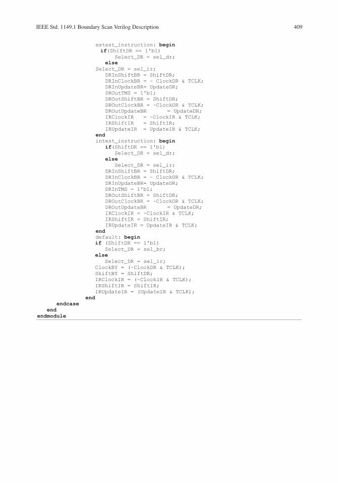
The complete Verilog description for the Standard IEEE 1149.1 is included in this appendix. This code was described in Chap. 8 and used in examples of this chapter.
Appendix DIEEE Std. 1149.1 Boundary Scan Verilog Description

404 IEEE Std. 1149.1 Boundary Scan Verilog Description

405IEEE Std. 1149.1 Boundary Scan Verilog Description

406 IEEE Std. 1149.1 Boundary Scan Verilog Description

407IEEE Std. 1149.1 Boundary Scan Verilog Description

408 IEEE Std. 1149.1 Boundary Scan Verilog Description
409IEEE Std. 1149.1 Boundary Scan Verilog Description

411
What follows is the Verilog code of the virtual tester discussed in Chap. 8. This is brought here for reference when studying the details of events taking place in the example of Chap. 8. Furthermore, this test bench can be used as a virtual tester template for other circuits with the Standard IEEE std. 1149.1 boundary scan. In which case, only the size of test data and response will have to be set according to those of CUT.
Appendix EBoundary Scan IEEE std. 1149.1 Virtual Tester

412 Boundary Scan IEEE std. 1149.1 Virtual Tester

413Boundary Scan IEEE std. 1149.1 Virtual Tester

414 Boundary Scan IEEE std. 1149.1 Virtual Tester

415Boundary Scan IEEE std. 1149.1 Virtual Tester
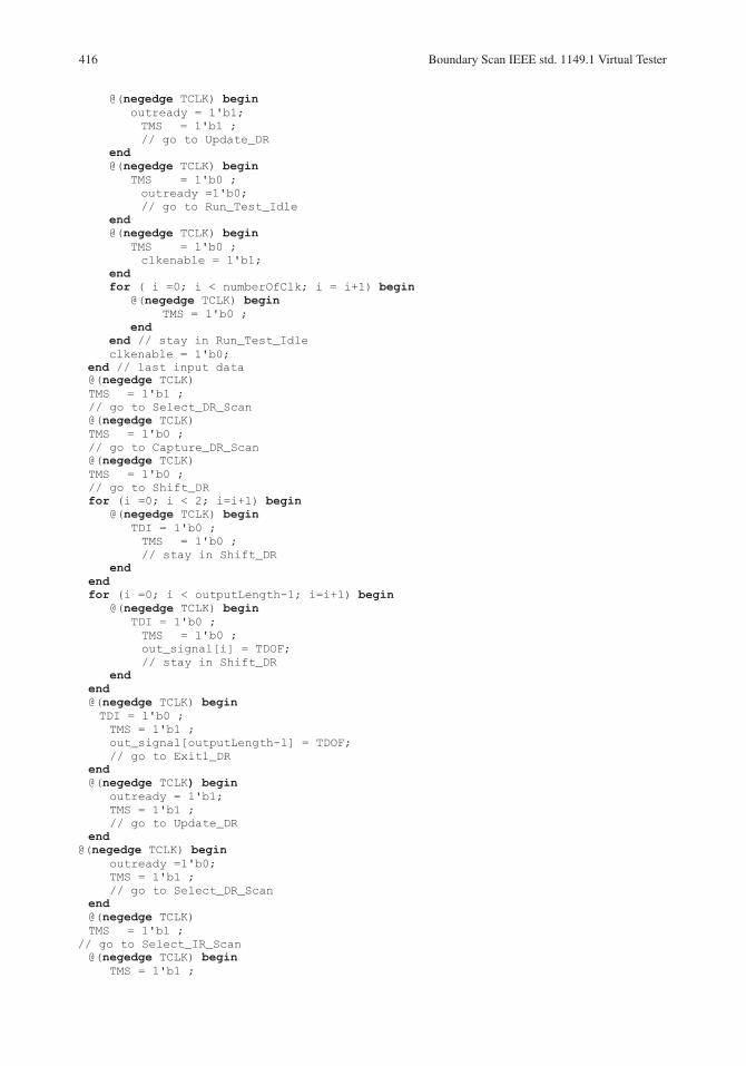
416 Boundary Scan IEEE std. 1149.1 Virtual Tester

417Boundary Scan IEEE std. 1149.1 Virtual Tester
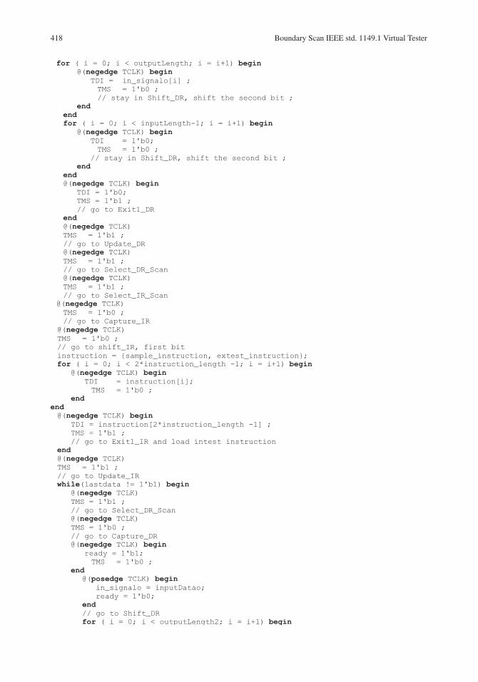
418 Boundary Scan IEEE std. 1149.1 Virtual Tester

419Boundary Scan IEEE std. 1149.1 Virtual Tester

420 Boundary Scan IEEE std. 1149.1 Virtual Tester
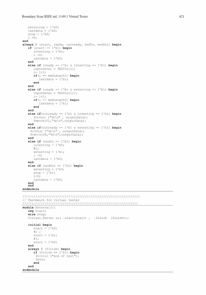
421Boundary Scan IEEE std. 1149.1 Virtual Tester
423
In order to perform test applications such as fault collapsing and fault simulation that have been done in many instances in this book, a netlist of primitive logic gates is needed. To be able to obtain this netlist from register transfer level (RTL) descriptions, a synthesis program is required. The synthesis program must be able to generate its hardware using our gate primitives (Appendix B) in order for our PLI functions (Appendix C) to be able to perform their test related tasks. For this purpose, NetlistGen1 that is a netlist generation program has been developed. In the background, NetlistGen uses the Web Version of Xilinx ISE (free version) for RT level synthesis, and it translates its intermediate NGC output of the synthesized design into the netlist required by test PLI functions. The end result is a synthesis program going from synthesizable Verilog code to a netlist of primi-tives. This appendix shows the procedures for installing and using this program.
F.1 Installing and Configuring NetlistGen
For using the netlist generator you should first install Xilinx ISE web pack edition. The installation process is listed below:
Download Windows based Xilinx ISE web pack edition from: · http://www.xilinx.com.Click on “setup.exe” and follow the setup process. ·
– Choose Web Pack edition for installation.– Leave the default options of checked boxes unchanged.– Click on the install button to start installation.
F.2 Synthesis and Netlist Generation
After installing Xilinx ISE, for generating a Verilog netlist from a behavioral Verilog code, the NetlistGen.exe file should be copied in the location as the behavioral description of your Verilog file. A partial Verilog code showing the required input/output format and a part of the RT level behavioral code is shown in Fig. F.1.
Appendix FGenerating Netlist by Register Transfer Level Synthesis (NetlistGen)
1This program has been developed by Hashem Haghbayan.

424 Generating Netlist by Register Transfer Level Synthesis (NetlistGen)
As shown, port declaration format for behavioral top module should list input output declarations after the module header. NetlistGen cannot translate input or output in the port identifier list. Same applies to port reg declarations.
When the RT level input is prepared as above, the following steps will result in the generation of a netlist.
Run · NetlistGen.When prompted, choose a name for your project. This name will become the project name of the ·synthesis process of ISE.When prompted for the name of the module, enter the name of the top level module of your ·project. The name of the Verilog file of the top level module should be the same as the name of the module. After that, NetlistGen reads the behavioral Verilog file. If you want to add any other Verilog files to your design, you can add them in the next step. Added files should be available in the root directory.Now you should synthesize your design with Xilinx ISE. For that, choose “y” to synthesize your ·design. For netlist generation, the NetlistGen_V2 netlist generator uses the intermediate EDIF format that is obtained from Xilinx Synthesis Technology (xse.exe) NGC output.When running · NetlistGen_V2, ISE installation path must be known. For this, ISE version 12.2 path is assumed. Enter the proper installation path if you are using a different ISE version.After selecting the location of ISE installation, the synthesis process will start. The process will ·be completed successfully if there are no compilation and synthesis errors.
· NetlistGen will generate the netlist in the netlist_MODULENAME_V1.v file. Part of what is automatically generated for example of Fig. F.1 is shown in Fig. F.2.
module Controller ( reset, clk, op_code, rd_mem, wr_mem, ir_on_adr, pc_on_adr, . . . . . . input clk; input[1:0]op_code ; output rd_mem; output wr_mem; output ir_on_adr; output pc_on_adr; . . . reg [1:0] present_state, next_state;
always @( posedge clk ) if( reset ) present_state <= `Reset; else present_state <= next_state; always @(present_state) begin . . . case( present_state ) . . . `Fetch : begin next_state = `WaitState; pc_on_adr=1'b1; rd_mem=1'b1; data_on_dbus=1'b1; ld_ir=1'b1; inc_pc=1; end . . . endcase endendmodule
Fig. F.1 Port declaration format and sample RT level code

425F.2 Synthesis and Netlist Generation
module Controller_net(global_reset, reset, clk,op_code,rd_mem,wr_mem,. . . input clk; input[1:0]op_code ; . . . output rd_mem; output wr_mem; wire_2_4,wire_2_5;
pin #(2) pin_0 ({op_code[0], op_code[1]}, {op_code_0, op_code_1});
fanout_n #(2, 0, 0) FANOUT_8 (wire_8, {wire_8_0, wire_8_1}); fanout_n #(2, 0, 0) FANOUT_9 (wire_9, {wire_9_0, wire_9_1}); fanout_n #(8, 0, 0) FANOUT_10 (wire_3, {wire_3_0, wire_3_1, wire_3_2, wire_3_3, wire_3_4,. . . and_n #(2, 0, 0) AND_11 (pc_on_adr, {wire_2_4, wire_4_4}); notg #(0, 0) NOT_6 (wire_11, reset); and_n #(2, 0, 0) AND_12 (wire_10, {wire_2_5, wire_11_0}); and_n #(2, 0, 0) AND_13 (wire_13, {wire_11_1, wire_4_5}); or_n #(2, 0, 0) OR_4 (rd_mem, {wire_8_1, wire_7_2}); and_n #(4, 0, 0) AND_15 (wr_mem, {op_code_0_4, wire_1_8, wire_3_7, wire_6_3}); dff INS_1 (wire_3, wire_10, clk, 1'b0, 1'b0, 1'b1, NbarT, Si, global_reset); dff INS_2 (wire_2, wire_12, clk, 1'b0, 1'b0, 1'b1, NbarT, Si, global_reset); endmodule
Fig. F.2 Netlist generated by NetlistGen

427
AAC, 8, 17–18, 43, 47, 66, 67, 253, 255, 330Access routine, 56–58AC test, 8, 17Activation, 47, 83, 84, 112, 127, 131–133, 135, 178,
180–182, 186, 188, 190–193, 195, 200, 214, 219, 222, 271, 276, 302
Adding BIST components, 342Adding BIST hardware, 332, 333Ad Hoc testability, 12Adjustable expected coverage-per-test, 167–170Aliasing, 117, 119, 122, 297, 299, 312, 314, 318, 320,
322, 340Analog converter, 18AND-bridging faults, 74Appearance fault, 67, 88, 111, 112, 135Arbitrary waveform generator, 17Architecture design, 298Asynchronous reset, 214, 234, 264, 302Asynchronous set, 214ATE. See Automatic test equipmentATE architecture and instrumentation, 17–19ATPG. See Automatic test pattern generationAt-speed testing, 8Automatic test equipment (ATE), 7, 8, 13–20, 53, 223,
224, 238, 257, 261, 281, 285, 292, 294–299, 325, 329, 345
Automatic test pattern generation (ATPG), 116, 143, 201, 204, 209, 211, 235, 347, 357, 359
AWG. See Arbitrary waveform generator
BBacktrace, 194, 197Backtracing, 195–197Backtrack, 187, 196Bandwidth, 345Basic CPT implementation, 137–138Basic PODEM, 191–193Basic TG procedure, 177–180Bed-of-nails probing, 261Behavioral description, 3, 29, 104, 105, 107, 108, 154,
229, 234, 236, 253, 335Behavioral level, 29, 30Behavioral level simulation, 15
Behavioral model, 5, 24, 236Behavioral testbench, 55BEST. See Built-in evaluation and self-testBF. See Bridging faultBidirectional pin, 266Bidirectional signal, 18Bidirectional signal power, 18Bidirectional switches, 77, 78BILBO. See Built-in logic block observerBILBO test process, 329Binary counter, 300, 301, 303Binding, 343BIST. See Built-in self-testBISTed CUT model, 335, 342Bit line (BL), 258, 377, 378Black box, 213Block coverage, 54, 56Board level, 12, 261277–281, 320–321, 326Bonding, 14Boolean difference, 72, 143–145Boolean equation, 157Boolean expression, 29, 30, 32, 36Boolean function, 29, 30, 71, 83, 94, 145Boundary register, 265, 266, 268, 270–273, 275, 276,
281, 283, 287, 290, 291, 324, 325Boundary scan
standard, 261–264, 275, 290, 292Boundary scan description language (BSDL), 261,
290–292Branch coverage, 54Bridging effect, 73, 310Bridging fault, 73–76, 84–87, 378Broadcast scan, 357–361, 372BSDL. See Boundary scan description languageBuffer memory, 270Built-in evaluation and self-test (BEST), 321–322Built-in logic block observer (BILBO), 320, 328–329Built-in self-test (BIST)
architectures, 16, 295–298, 312, 317, 319–330, 343, 383
controller, 295, 297–300, 312–314, 317–321, 323, 325, 327, 330, 332–335, 337–339, 342, 343, 384
procedure, 299, 300, 312, 320, 343tester, 384
Bus conflict, 262
Index
Z. Navabi, Digital System Test and Testable Design: Using HDL Models and Architectures,DOI 10.1007/978-1-4419-7548-5, © Springer Science+Business Media, LLC 2011

428 Index
BYPASS instruction, 272, 273, 282, 287Bypass register, 265, 272, 283
CCapture, 224, 264–266, 268, 269, 271, 272, 275, 276,
278, 287, 288, 291, 325, 329, 334, 340Catastrophic failure, 7, 8CB(l), 156CC0(l), See. Combinational 0-controllability of line lCC1(l), See. Combinational 1-controllability of line lCell coupling, 378Channel, 17, 18, 357, 359, 360, 362, 363, 368, 369Channel capacity, 345Characteristic polynomial, 304, 306Characteristics, 4, 105Chip
level, 277, 279, 326manufacturing, 3–4testing, 6, 12, 14–15, 261, 324
Circuit level, 10, 15, 35, 69, 71, 82, 89, 95, 103, 106, 113, 154, 231
Circuits without reconvergent fanout, 150–Clock enable, 251, 312, 332, 333, 367, 377Clock rate, 11Cluster, 244CMOS, 30, 31, 65, 77–79, 228Code-based decompression, 366–371Code-based schemes, 347–363, 366Codeword, 347, 349–356, 364, 366–369, 371Column addresses, 253, 376Combinational circuit RTG, 163–170Combinational controllability, 155, 156, 160Combinational 0-controllability of line l (CC0(l)), 155Combinational 1-controllability of line l (CC1(l)), 155Combinational fault simulation, 111Combinational observability, 156, 160Combinational test generation, 234, 244, 248–250, 258Combinational TPG, 237–238Compaction, 11, 147, 175, 200–211, 345Compact test vectors, 9, 11, 201, 205Compatibility, 201–205Complexity, 8, 20, 36, 69, 122, 123, 141, 143, 145, 155,
172, 206, 261, 285, 345, 366, 378, 381, 387Compression, 24, 119, 120, 122, 312, 345–347Concurrent BIST (CBIST), 298, 326–328Concurrent fault simulation, 131–133Concurrent testing, 8, 201, 203Concurrent testing (ATE), 8Concurrent testing (Online), 8Cone, 140, 162, 196, 300, 301Confidence level, 161, 162Configurable LFSR, 309–311, 329, 332Conjunction, 359Consistency, 266Continuous waveform testing, 18Controllability, 10, 12, 146–157, 159, 160, 162, 163,
213, 217, 218, 225, 227, 261, 319, 322, 325, 3570-Controllability, 156, 159, 2181-Controllability, 156, 159, 218
Controlling event, 299Control point, 220, 221Control registers, 267, 282, 283Control value, 147–149, 156, 195, 197, 217Convergence, 56, 91, 138, 140, 151Core isolation, 12, 261, 262Cost of test, 13, 14, 261, 345Coupled cell, 378Coupling, 378Coverage expectation graph, 170Critical path
faults, 137tracing, 137, 197tracing fault simulation, 141–144
Cross-coupled, 227CSBL
Hardware, 320test process, 321
CSC. See Cyclical scan chainCube, 182–184, 186–190, 191, 354, 361, 362CUT. See Circuit-under-testCyclical scan chain, 363, 365–366
DD-Algorithm, 182–191, 194, 196, 197, 199Data polynomial, 308Data retention fault, 387DC
instrumentation, 17test, 8
D-cube, 184–187, 189, 191Decoder, 216, 219, 262, 271, 272, 281–283, 301,
345–347, 349, 351, 362–371, 376, 377, 383, 386–387, 389, 391
Decompressionhardware, 345, 347, 362–365, 372methods, 362–371unit, 348, 363
Deductive fault simulation, 133–137Defect, 3, 7, 10, 63–101Defect coverage, 73Delay element, 214, 302Design and test, 21–62Design error, 1Design for test, 26, 141, 281Design rules, 261Design validation, 234–235Detection, 24, 86, 112, 114, 116, 124, 135, 137, 140,
145–147, 152–153, 161–163, 166, 178, 182, 198, 206, 208, 311
Detection probability, 152–153, 162–163Deterministic search, 145Deterministic test generation, 175–211Developing a virtual tester, 234, 238–244, 292Device identification register, 265Device under test (DUT), 5–7, 16–19, 95, 97DFF. See D flip-flopD
f-hard 1,, 161
Df-hard N
, 161
[Au1]
429Index
D-frontier, 186–190, 194, 197DFT, 21, 27, 56, 141, 205, 213–258, 281, 295, 296, 330Diagnosis, 112, 117, 122Dictionary-based, 346, 351–354, 359, 368–370Differential fault simulation, 140–141Digital stimulus and measure instruments, 17Digitizer, 17Disjoint compatibility, 204Distances based,160Disturb BIST structure, 389–391Disturb BIST Walking-0, 389Disturb MBIST, 387–389D-notation, 178Dominance fault collapsing, 92–95Dominate, 92–94Don’t care, 347, 355, 356, 363DRAM, 15, 375, 376, 387Dual clocking, 229–231DUT, See Device under testDynamic compaction, 209–211Dynamic RAM, 375Dynamic test, 201, 209
EEEPROM, 375Electrical fault, 17Embedded, 16–19Engaging ORAs, 312Engaging TPGs, 300, 301Equivalence checker, 3Equivalent fault, 86, 87, 91, 92Equivalent single stuck-at faults, 86, 87Erasable PROM (EPROM), 375Estimating hardest detection, 162Evaluate test vectors, 9, 163Exhaustive, 87, 118, 145, 160, 162, 296, 300, 301, 378Exhaustive counters, 300–301Exhaustive test, 300, 301, 378Expected response, 4, 5, 48, 53, 241, 251, 295Expected result, 9Expected signature, 316, 318, 320, 321, 323, 327External testing, 8EXTEST instruction, 275–278, 286
FFabrication, 14Failure, 7, 8, 14, 63, 186, 187, 195, 327, 328, 377FAN. See Fanout oriented test generation algorithmFanout branch, 72, 92, 139, 150, 157, 195Fanout free, 94–95, 150, 151, 196, 198Fanout stem, 72, 91, 92, 138, 150, 151, 157, 198, 217Fanout oriented test generation algorithm, 196–197Fast Fourier transform (FFT), 19Fault
activation, 112, 178, 181blocking, 112collapsing, 10, 25, 86–101, 107, 108, 113, 114, 164,
215, 236, 241, 242
coverage, 10, 11, 26, 27, 55, 86, 112–115, 119, 163, 164, 166, 167, 170, 172, 174, 176, 201, 202, 205–209, 213, 236, 238, 258, 296–300, 319, 322, 324, 325, 329, 330, 332, 336, 338, 349, 357–359
coverage procedure, 113–114cubes, 185detection, 24, 112, 146, 178, 311diagnosis, 117, 122dictionary, 26, 111, 113, 114, 117–122dominance, 92, 93dropping, 111, 113, 114, 118, 125, 130, 137, 140,
166, 168, 169, 205effect, 15, 83, 119, 131, 171, 177, 178, 185, 186, 216equivalence, 86, 87, 140independent test generation, 146, 147, 197–198list, 24–25, 95, 96, 101, 104, 105, 107–110, 113,
114, 118, 131, 133–137, 140, 163, 166, 205, 210, 238, 338
list compilation, 24–25model, 10, 24, 25, 63–101, 103, 104, 147, 176,
376–378oriented test generation, 116–117, 146, 147, 160,
174–177, 197, 198propagation, 112, 131–135, 179, 191reduction, 10, 101simulation, 10, 11, 25–26, 55, 56, 80, 95, 96,
103–141, 158, 163, 164, 171, 175, 177, 197, 201, 205–207, 210, 236, 297–299, 322, 324, 325, 329, 330, 336–339
simulation requirements, 104–105simulation technologies, 122–141
Faultable, 26, 62, 104, 107–109, 113, 114, 118, 128, 147, 164, 171, 206
Fault injection (FI), 25, 59–62, 96, 104, 107, 109–111, 124, 127–130, 140, 169, 173, 207, 208, 242
Fault removal (FR), 59–61, 109Faulty, 10, 24–26, 60, 65–69, 71–84, 86, 92, 94,
103–105, 108, 110–114, 116–119, 121–125, 127, 130, 132, 133, 143–145, 171, 177, 178, 200, 207, 241, 397
Feedback, 40, 159, 214–216, 226–229, 233, 236, 238, 244–246, 248, 250, 253, 302–304, 316, 317, 319, 321–324, 328, 339, 365
flip-flop, 214, 238, 248, 253, 323path, 227, 228, 248, 304, 316register, 214, 215, 226, 229, 233, 244–246, 248,
322–325, 328FFT. See fast Fourier transformFI. See Fault injectionFinite state machine (FSM), 36, 37, 40, 218, 366–370Fixed expected coverage, 163–167Flaw, 2, 3, 63Floating, 263Formal, 3, 72, 111, 145, 177, 178, 180–182Fourier, 19FPGA, 16, 235FR. See Fault removalFrequency, 7–9, 17, 18, 51, 291, 303, 306, 349–351FSM. See Finite state machine

430 Index
Full scan, 225, 226, 234, 238, 241, 244, 245, 248–251, 253–255, 329, 330, 358
design, 234–245, 248, 250, 252DFT technique, 225–246insertion, 226–227
Functional fault, 67–68, 71, 83, 377Functional level, 67Functional model, 146Functional test, 5, 176, 234, 235, 277, 378–379Functional test generation, 5, 176Functionally equivalent, 86
GGate fault list propagation, 134–135Gate faults, 87–89, 134–135Gate level
fault, 65, 66, 71–86, 100, 105fault simulation, 55, 103–104simulation, 55, 105, 107, 124
Gate oriented fault collapsing, 87–90Generator, 17, 174, 298, 308, 319, 389, 390Generic parameter, 291Generic TAP controller, 283Glitch, 267Golomb, 355–357, 365, 371Good signature, 330, 336–338Gross data retention fault, 387Guided probe testing, 8
HHandshaking, 18, 48Hard-to-detect fault, 146, 162, 311Hardware description language (HDL)
based fault coverage, 114Hardware modeling, 15Hardware testing, 117, 122, 295Hazard, 231Hazard removal, 85HDL. See Hardware description languageHeuristic, 145, 163, 186, 195, 196Hierarchical naming, 52Hierarchical scan, 292Higher levels of abstraction, 32, 67, 68High level, 1, 17, 23, 55, 197, 238High speed, 17Huffman codes, 349–351, 366, 368Huffman model, 40, 41, 214, 226, 227, 229, 234, 236,
245, 249, 253, 254, 258, 320, 322, 324, 325, 328Huffman tree, 349–351, 367, 368Hybrid BIST, 298, 308, 309, 325, 327
IIdempotent coupling, 378IEEE standard, 22, 261–294Illinois scan, 358–360, 372Implication, 180–182, 191, 193Improving controllability, 12, 213, 217–218, 261, 265
Improving observability, 12, 213, 216, 261, 265In-circuit testing, 8, 261Incompatible, 201Initialization, 29, 290, 299Initial state, 267, 368Initial statement, 49, 51, 52, 95, 242, 336, 337Inject fault, 15, 25, 26, 59–62, 104, 105, 107–111, 113,
114, 116, 118, 119, 123, 124, 127–131, 166, 169, 171, 173, 177, 182, 187, 199, 207, 208, 241, 242, 244, 338
Input cell, 266, 268, 271, 275, 277, 288, 325Instruction, 42–44, 47, 65–67, 261–268, 271–276, 278,
279, 281–283, 286, 287, 290, 291, 294Instruction fault, 67Instruction register (IR), 43–45, 47, 253, 255, 264–273,
275, 281–283, 287, 291, 332Integrated circuit, 14, 122Integrated liquid cooling system, 18Interconnection, 2, 3, 5, 14, 29, 30, 32, 68, 69, 71, 226,
275, 286Internal testing, 8Internal-XOR LFSR, 307Intersection, 135, 184Intersection of fault lists, 135Intest instruction, 272, 275–277, 286, 287Inversion coupling, 378IP core, 141, 345IR, See Instruction registerIsolated serial scan, 223–225
JJoint test action group (JTAG), 261Jumper, 12, 215Justification, 77, 180–182, 184, 186–191, 199
KKarnaugh map, 71–74, 84, 85, 182K-cell coupling, 378
LLatch, 41, 227–229, 231–233Layout, 3, 8, 64Least significant, 253, 268, 330, 381, 383, 386Level sensitive scan design (LSSD), 233,
324–325Linear feedback shift register (LFSR)
characteristic equation, 304cycle, 305, 307, 308, 330, 338with serial input, 308–309, 316
Linear system, 362Line oriented fault collapsing, 89–91, 97Logic BIST, 295, 343, 345Lookup, 9, 122, 369, 383, 387Lookup memory, 383LSSD, See Level sensitive scan designLSSD on-chip self test (LOCST), 324–326Lumped, 69, 71, 253

431Index
MMandatory instruction, 264, 265, 271–277, 281Manufacturing test, 1, 3, 7, 14, 17, 19–20, 235MARCH A, 380–381MARCH B, 380–381MARCH C, 380–381March C
algorithm, 379–380BIST counter, 382, 386, 388MBIST, 385–389
Marching-1, 302March test, 378–381, 387MARCH X test, 380–381MARCH Y test, 380–381Mask misalignment, 64, 65Mass storage, 271Master, 229, 231–233, 337Master/slave flip-flop, 229MATS+, 380–381MATS++, 380–381MATS test, 380–381Maximum-length LFSR, 306–308MBIST. See Memory BISTMealy machine, 36, 37, 40, 199, 216Measurement, 10, 18, 19, 25–27, 56Memory
based BIST, 295–297cell, 375–378, 380, 387, 389fault model, 375, 377–378read operation, 47, 376, 377, 379–381, 384, 386structure, 375–377, 381, 390test, 302, 375–391write operation, 376, 377, 379–381, 384, 386
Memory BIST (MBIST), 296, 375–391MISR. See Multi-input signature registerMode control, 216, 217, 253, 266, 275, 276, 329Modular LFSR, 307–308Modulo, 37, 304, 305, 308, 314, 356Moore’s law, 8MOS, 30Multi-input signature register (MISR), 119, 121,
317–320, 322, 323, 325–330, 332–334, 337, 338, 340, 341, 358
Multiple fault, 75–77, 82, 83, 117, 122, 127, 128, 146, 176
Multiple-input broadcast scan, 359–360, 372Multiple observe points, 218Multiple path, 182, 185Multiple scan
architecture, 251–253chains, 278–281, 347, 353, 354, 357–359design, 251–254, 329test procedure, 252
Multiple sensitized paths, 181–182, 190Multiplexed test data, 229
NNail, 261Neighboring cores, 261
Neighboring gates, 73Netlist, 3–5, 23, 24, 26, 27, 56, 95, 104, 105, 107, 112,
123, 124, 128, 129, 154, 158, 229, 234–237, 241, 253, 256, 283, 330, 332, 335, 341
Netlist Gen, 107, 234–236nMOS, 30, 64, 68, 77, 79, 80Noise, 18, 19Nonblocking assignment, 52Non-controlling value, 195Non-faulty gate, 67Non-functional module, 283Non-invasive mode, 262, 272Non-invasive operation, 266Non-overlapping, 228Non-polynomial, 145Non-volatile, 375Non-zero, 305NP-complete, 11, 250
OObjective, 56, 194, 196Observability, 10, 12, 146–150, 152, 154–157, 159, 160,
163, 174, 194, 195, 213, 215, 216, 218, 225, 261, 265, 299, 319, 322, 328, 331, 363
Observation point, 218, 221Offline BIST, 297Offline testing, 8One-controllability, 147–149One-hot, 301, 302One’s counting, 314Online BIST, 297–298, 304OR bridging fault, 74–76, 84–86
PPackage, 14, 262, 292Package level, 14Parallel fault simulation, 127–133Parallel load/loading, 214, 223, 224, 268, 276, 300Parallel mode, 253, 323, 331, 334, 335, 358Parallel scan, 251, 252, 255, 363Parallel serial full scan (PSFS), 358Parallel shift-register sequence generator (SRSG), 317,
319, 322, 323, 325, 332, 333Parallel signature analysis, 317–319Parallel synchronizer, 368Parallel to serial converter, 364Parity checking, 316Partial scan, 248–251Partitioning combinational circuit, 300Partitioning test data, 347, 348Path coverage, 56Path oriented test generation (PODEM), 191–196Path sensitization, 181, 185Pattern generator, 319, 389, 390Pattern memory, 17, 18PCB. See Printed circuit boardPerformance, 2, 7, 8, 14, 17, 123, 127, 128, 130,
248, 271

432 Index
Periodic, 48, 50, 51, 54, 242Period of linear feedback shift register, 303–311Permanent, 69, 71, 86, 377Physical level, 64PI. See Primary inputPipeline circuit, 321PLI. See Procedural language interfacepMOS, 68, 77, 79–81PODEM. See Path oriented test generation0-Point cube, 1831-Point cube, 183, 184Polynomial, 304–310, 316–318, 320, 322, 324, 330,
336–339Posedge, 36, 53, 114, 171, 207Post manufacturing test, 4, 5, 20, 21, 143, 234, 235, 242Power consumption, 27, 213, 215Power level, 17Power management, 14, 17Power supply, 19Precalculated expected coverage-per-test, 170Prefix-free, 351, 367Present state, 39, 45, 47, 227, 245, 246, 328Previous time frame, 200Primary input (PI)
combinational controllability, 155sequential controllability, 155
Primary output (PO), 10, 83, 90, 111, 137, 145, 148, 150, 156, 158, 159, 162, 171, 177–179, 181, 190–193, 196, 197, 199, 200, 213, 214, 216, 217, 227, 244, 246, 248, 254, 322–325, 329, 330, 332, 340
Prime cubes, 183, 184Primitive, 29–32, 35, 57, 88, 97, 107, 128, 182,
184–187, 189, 197, 215, 236, 237, 306Primitive cube, 182–184, 186, 187, 190, 191Primitive polynomial, 306, 307Printed circuit board (PCB), 122, 261Probability based controllability and observability,
148–150Probe, 261Probe test, 8Procedural language interface (PLI), 16, 21, 56–59,
62, 95, 97, 108, 109, 114, 128, 154, 158, 208, 236, 338
Production, 13, 19, 299Programmable register structure, 311Programmable ROM, 375Programmable threshold, 17Programmable voltage level, 17Propagate cube, 184Propagate fault, 131, 177, 178, 186Propagation, 15, 31, 110, 112, 119, 123, 132,
134–137, 178–182, 184–187, 189, 191, 193, 194, 199, 200, 230
Propagation D-cube, 184, 189, 191Protocol aware ATE, 16PRPG. See Pseudo random pattern generatorPseudo code, 59, 187, 190, 192, 194, 197, 206, 224Pseudoinput, 215, 227, 237, 250, 258, 325Pseudooutput, 244, 250
Pseudo primary input (PPI), 237, 250, 254Pseudo primary output (PPO), 215, 227, 254Pseudo random pattern generator (PRPG), 319–323,
325, 327, 328, 330, 333Pseudo random sequence generator, 319Pseudo-random serial test data, 317, 325Pseudo-random test patterns, 300Pseudo-static latch, 228PSFS. See Parallel serial full scan
QQuality, 14, 19, 54, 143Quotient polynomial, 309
RRace, 3Radiation, 63RAM. See Random access memoryRandom access memory (RAM), 384, 390Random access scan, 253Random pattern generator, 319 Random search, 145Random sequence generator, 319 Random test generation (RTG), 114, 116, 146, 155, 160,
174, 175, 201, 205, 206, 210, 211Random test socket (RTS)
BIST insertion, 330–335hardware, 322–323
Random time intervals, 52–53Read only memory (ROM), 381Recognizing faults, 71–72Reconvergent fanout, 91–92, 138, 140, 149–151, 154,
155, 163, 181, 182, 217Recursive function, 97Recursive process, 197Redundant fault, 85–86Redundant test vector, 205Register transfer level (RTL)
BIST design, 329–330design full scan, 235–238design multiple scan, 251–252design process, 1, 7, 13, 15, 16, 21scan design, 253, 258simulation, 2, 10synthesis, 2–3
Reliability, 8, 85, 381Remainder polynomial, 309Residue-5, 37, 41, 50, 114, 119, 121, 171, 172, 206,
211, 234, 238, 241, 244, 254Resistive wire, 3Reverse order fault simulation, 205RF, 17Ring counter, 301–303Rise and fall delays, 35ROM. See Read only memoryRoot, 349Row decoder, 377RTG. See Random test generation

433Index
RTL. See Register transfer levelRTS. See Random test socketRule of ten, 13RUNBIST, 321, 323, 331Run-length, 347, 361, 362, 365, 370–371
SSA0, 77, 79, 82, 84, 87–91, 94, 112, 131, 134, 137, 140,
144–146, 152, 177, 178, 180, 181, 187–191, 195, 196, 198–200, 216
SA1, 77, 79, 81–89, 91–94, 112, 131, 135, 139, 148, 160, 181, 182, 190, 192, 193
SAMPLE instruction, 272–274Sampling, 272Sampling process, 320Sandia Controllability/Observability Analysis Program
(SCOAP)combinational parameters, 155–158controllability and observability, 155–160, 194sequential parameters, 155, 158–160
SB(l), 159SC0(l), 159SC1(l), 159Scan architectures, 225, 244–253, 262–271, 278, 279,
297, 358–361Scan-based decompression, 363, 372Scan chain, 27, 239, 241, 245, 248, 251, 252,
255–258, 265, 272, 277–281, 284–286, 292, 320, 324, 325, 330, 341, 342, 345, 347, 348, 353, 354, 357–368, 372
Scan design, 234–245, 248–254, 258, 291, 298, 299, 329, 357
Scan designs for RTL, 253–258Scan flip-flop, 231, 238, 244, 253, 254, 262, 276Scan in, 358, 359Scan insertion, 12, 226–227, 234, 238, 253, 258,
330–332Scan mode, 358Scan out, 325Scan path, 233, 248, 254, 272, 286Scan register, 226–227, 229, 230, 251, 261, 262, 265–266,
270–272, 275–277, 281, 283, 287, 290, 291, 294, 310, 324–326, 328, 334, 340–342, 367, 369
Scan testability rules, 271–277Scan testing, 17, 226, 234, 250–251, 254, 262, 271–277,
281–283, 298, 323SCOAP. See Sandia Controllability/Observability
Analysis ProgramSearch space, 145, 191Seed, 119, 309, 310, 318, 324, 325, 336, 338, 339,
361, 362Segment, 11, 17, 18, 138, 171, 251, 252, 326, 340Selection, 49, 117, 146, 160, 163, 166, 180, 191, 192,
194, 196, 197, 205, 221, 227, 231, 248, 250, 271, 299, 312, 376
Selective Huffman, 351, 363, 366–368Self-test, 267, 321–322, 325–326Semiconductor, 399Sense amplifier, 376
Sensitivity list, 33, 36, 39Sensitization, 181, 185, 190Sensitized path, 179–182, 190, 197Sequential circuit
fault coverage, 114fault dictionary, 114, 119–121fault simulation, 111Huffman model, 40–41, 214, 226, 253random test generation (RTG), 143, 171–174, 210test generation, 143–147, 171, 172, 175–200, 210,
213, 214, 225, 236, 258Sequential controllability, 155, 159, 160Sequential 0-controllability of line l, 159Sequential 1-controllability of line l, 159Sequential observability, 159, 160Sequential observability of line l, 159Sequential SCOAP parameter, 158–160Sequential testbench, 50–51Serial access, 245Serial fault simulation, 124–128, 130, 137, 140Serial input signature analyzer (SISA), 319, 322, 323,
330, 332, 333, 336–338Serial input signature register (SISR), 316–317,
319–324, 325Serial LFSRs, 316–317Serial load, 226Serial parallel shift register, 224, 226Serial synchronizer, 364, 370, 371Settling time, 111Shadow architecture, 245Shadow register, 245–248Sharing control pins, 219–221Sharing observability pins, 218–219Signature, 24, 26, 119, 297, 299, 308, 312–314,
316–323, 325, 327, 330, 332–334, 336–338, 340Signature analysis, 317–319, 332Silicon, 14, 290Simple march BIST, 381–385Simplified D-algorithm, 190Simultaneous control and observation, 222–225Single fault, 77, 82–83, 128Single stuck-at fault, 83, 86–87, 103, 104, 122, 134,
140, 147, 176Single stuck-at structural fault, 77–83SISA. See Serial input signature analyzerSISR. See Serial input signature registerSlave, 229, 231–233Slow clock, 229, 248SOC. See System on chipSOCRATES, 197Spectral analysis, 19SRSG, 317, 319, 322–326, 330, 332, 333, 336Standard cell, 292Standard LFSR, 304–305, 307Standard test protocol, 263State coupling fault, 378State-dependent faults, 75State machine, 36–42, 44, 51, 52, 218, 262, 299, 300,
323, 366, 367, 369Statement coverage, 54, 56
AU2

434 Index
State transition, 38, 41, 370Static analysis, 155Static combinational compaction, 205Static compaction, 201, 204–209Static RAM (SRAM), 375–377Static sequential compaction, 206–209Stem, 72, 91, 92, 138, 139, 150, 151, 157, 198, 217Strobe, 17Structural fault, 68–72, 77–83, 377Structural gate level faults, 71–84, 103Structural test, 5Stuck-at fault, 60, 61, 77–81, 86–87, 103, 104, 107,
108, 122, 134, 137, 139, 140, 147, 171, 176, 297, 377, 378
Stuck-at-0 faults, 72, 73, 76, 77, 82, 84, 86, 108, 109, 145, 377
Stuck-at-1 faults, 69, 71, 73, 76, 77, 79, 81, 82, 85, 86Stuck-at models, 122, 135, 147Stuck-open fault, 72, 76, 79STUMPS, 325–327, 329, 330, 340–343Superposition, 304Supply, 19, 29, 73, 81Synchronizer, 345, 347, 363–371Synchronizing, 52, 271, 364, 365Synchronous, 41, 50, 214, 229Syndrome, 117–122Synthesis, 1–4, 22–24, 107, 112, 234–236, 238, 330, 347System clock, 51, 229, 288, 347, 353, 363–365, 367, 369System testing, 4, 9, 10, 15, 20, 141System on chip (SOC), 13–15, 18, 376
TTAP controller, 267–273, 275–278, 281–284,
286–288, 294Target fault, 360TCLK, 246, 248, 262, 267, 287, 288TDI. See Test Data InTDO. See Test Data OutTestability
analysis, 24–25hardware evaluation, 16insertion, 11, 14, 215–225measure, 143, 155measurement, 10, 25–27, 56methods, 8, 11–15, 20, 223
Testbench, 1–3, 16, 21–28, 48–56, 58–62, 77–79, 81, 95, 96, 109–111, 114, 118, 119, 121, 122, 127, 128, 130, 154, 158, 164, 166, 168–172, 206, 208, 209, 234, 235, 238, 241, 242, 254, 258, 286, 287, 330, 336, 337, 342, 343, 384, 386
Test compaction, 11, 147, 201, 205, 206, 208–211Test compatibility, 201–204Test compression, 345–372Test concerns, 1, 8–15Test controller, 18Test cube, 182, 187, 188, 347, 353, 354, 361, 362Test cycles, 143, 174, 320, 325, 326, 329, 330, 332–334,
336, 338, 339
Test data compaction, 200–211Test data compression, 345–347, 349Test Data In (TDI), 226, 263–266, 268, 272, 277–280,
286–288Test data memory, 296Test Data Out (TDO), 263, 265, 266, 268, 271–273,
277–280, 283, 286, 288Test effectiveness, 172Tester channel, 357, 359, 362, 363, 368, 369Testers, 5–9, 14, 16, 18, 19, 103, 108, 177, 206, 242,
254, 270, 346, 357, 359, 362–364, 367, 369, 371Test generation, 5, 10–11, 25–27, 56, 72, 82, 83, 95, 96,
108, 112–117, 143–147, 155, 163, 170–172, 174–178, 180–182, 184–186, 189, 191, 193, 195–197, 199–201, 204, 205, 209, 214, 215, 217, 225, 236, 238, 244, 248–250, 252–254, 258, 347, 357, 372
Test head, 18, 19Testing, 2, 21, 82, 111, 146, 200, 214, 261, 296, 357 Testing cost, 14Test logic, 223, 262, 263, 267, 286, 290Test methods, 8–12, 14–16, 21–22, 24, 37, 42, 83, 95,
214, 234, 261, 381Test mode select (TMS), 262, 267, 268, 270, 277, 279,
280, 286–288, 290Test pattern, 5, 300, 322, 347, 349, 350, 352–355,
357–360, 381, 383, 386, 387, 389Test pattern generators (TPGs), 116, 143–174, 296–312,
317, 319–321, 324, 328, 330, 332, 340, 343, 389, 396
Test plan, 238Test procedure, 24, 227, 234, 246–248, 250–253, 258,
285, 298, 299, 333, 343, 378–381Test program, 4, 5, 7, 21, 57, 100, 105, 234, 235, 238,
242, 257, 258, 261, 290, 295, 296, 298, 299Test refinement, 112, 114–116Test Reset (TRST), 262, 267, 291Test response memory, 297Test session, 319, 320, 322, 325, 327, 333, 334, 383, 384Test set
compatibility, 203–205verification, 234, 244
Test time, 1, 7, 9, 11–13, 16, 18, 20, 25, 27, 146, 147, 172, 203, 213, 215, 218, 221, 222, 230, 245, 248, 251, 253, 258, 277, 278, 296, 298, 318, 320, 325, 329, 336, 338, 343, 345, 359, 372, 378
Test vectorscompatibility, 201–202ordering, 206reordering, 202
THD, 18Thermal management, 18Threshold, 17, 210, 216Throughput, 14, 15, 18Time frame, 199, 200Time frame expansion, 199, 200TMS. See Test mode selectTotal cost, 13TPGs. See Test pattern generators

435Index
Transient fault, 81Transistor fault, 77, 79, 82Transition counter, 314–316Transition faults (TF), 378Transparent latch, 227Tree, 196, 349, 368Trial and error, 299Tri-state control, 216, 217Twisted ring counter, 302–303Two-phase test generation, 176–177, 211Two-port flip-flops, 231–234
UUndetectable fault, 85Unfolding, 214, 215, 226, 234, 236–238Unidirectional, 30Unique sensitized path, 197Unique syndrome, 117, 119Universal slot, 19Unspecified bit, 347, 349, 354UpdateDR, 269, 270, 273, 275, 276, 290User defined logic, 266User defined registers, 266, 272
VVerification, 2, 3, 23, 234, 244Verilog
model, 2, 23, 77, 231, 335testbench, 23–29, 48, 56, 77, 95–97, 106, 109, 114, 117,
118, 125, 154–155, 158, 164, 168, 169, 171, 174, 175, 206, 215, 237, 238, 241, 258, 285, 330, 336
VHDL, 53, 290, 291Virtual boundary scan tester, 285–290Virtual circuit, 127, 357, 358Virtual injection, 131Virtual parallel gate, 130Virtual tester, 16, 27, 48, 215, 224, 225, 234,
238–244, 254, 255, 257, 281, 285–287, 290, 292, 294, 296, 329
Visual inspection, 23
WWafer
level, 14prober, 7testing, 7
Walking-0, 387, 389–391Walking-1, 301, 302Waveform
digitizer, 17fidelity, 18generator, 17modulation, 18
Weighted LFSR, 311Word line, 377, 378
XX-path, 193–196
YYield, 14, 23, 172, 176, 305