application note #136 - nanowerk
TRANSCRIPT
Atomic force microscopy and Raman spectroscopy are both techniques used to gather information about the surface properties of a sample, yet their respective user base is often quite different. There are many important application reasons to combine these two technologies, and this application note looks both at the complementary information gained from both techniques and how a researcher having access to a combined system can benefit from the additional information available.
Atomic Force Microscopy
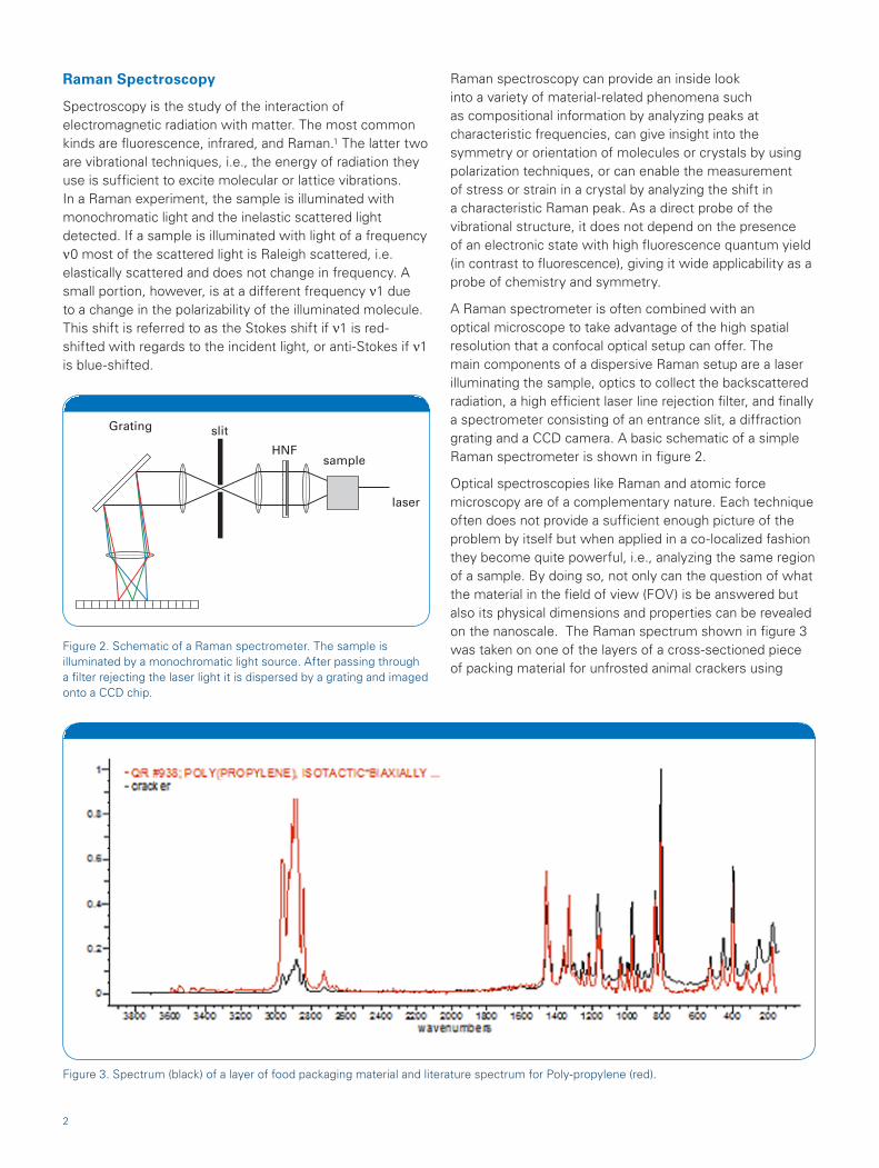
In atomic force microscopy a sharp probe is brought into close proximity with a sample and held at that distance by means of a force-based feedback loop. In addition to the force on which the primary feedback loop is based, different quantities such as electrical current, surface potential or specific nanomechanical properties can be measured. By scanning tip and sample relative to each other and measuring these quantities at discrete locations in a serial fashion, three-dimensional images of selected sample properties can be created. A generic atomic force microscope (AFM) setup is depicted in figure 1. The information that atomic force microscopy can provide has proven to be extremely useful for scientific research and industrial applications. They lack however, chemical specificity. That is, unless tip-sample forces are probed
as a function of chemical tip modification (i.e., Chemical Force Microscopy), which is an approach that can help characterize the distribution of known chemistries in specific cases but which has not been shown to provide the general applicability of vibrational spectroscopies.
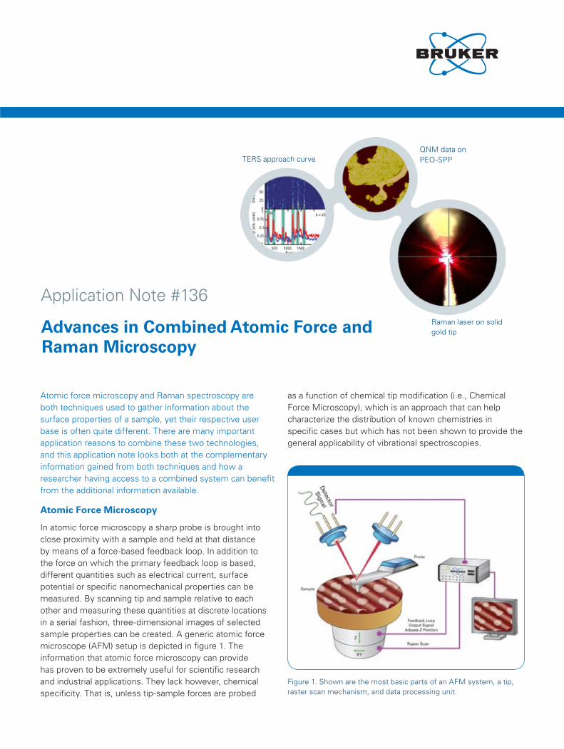
Application Note #136
Advances in Combined Atomic Force and Raman Microscopy
Raman laser on solid gold tip
TERS approach curveQNM data on PEO-SPP
©20
12 B
ruke
r C
orpo
ratio
n. A
ll rig
hts
rese
rved
. Bio
Sco
pe C
atal
yst,
Dim
ensi
on Ic
on, I
nnov
a, IR
IS, N
anoS
cope
, and
Tap
ping
Mod
e ar
e tr
adem
arks
or
regi
ster
ed t
rade
mar
ks o
f B
ruke
r C
orpo
ratio
n. A
ll ot
her
trad
emar
ks a
re t
he p
rope
rty
of t
heir
resp
ectiv
e co
mpa
nies
. AN
136,
Rev
. A2
Figure 1. Shown are the most basic parts of an AFM system, a tip, raster scan mechanism, and data processing unit.
Grating slit
HNFsample
laser
Raman spectroscopy can provide an inside look into a variety of material-related phenomena such as compositional information by analyzing peaks at characteristic frequencies, can give insight into the symmetry or orientation of molecules or crystals by using polarization techniques, or can enable the measurement of stress or strain in a crystal by analyzing the shift in a characteristic Raman peak. As a direct probe of the vibrational structure, it does not depend on the presence of an electronic state with high fluorescence quantum yield (in contrast to fluorescence), giving it wide applicability as a probe of chemistry and symmetry.
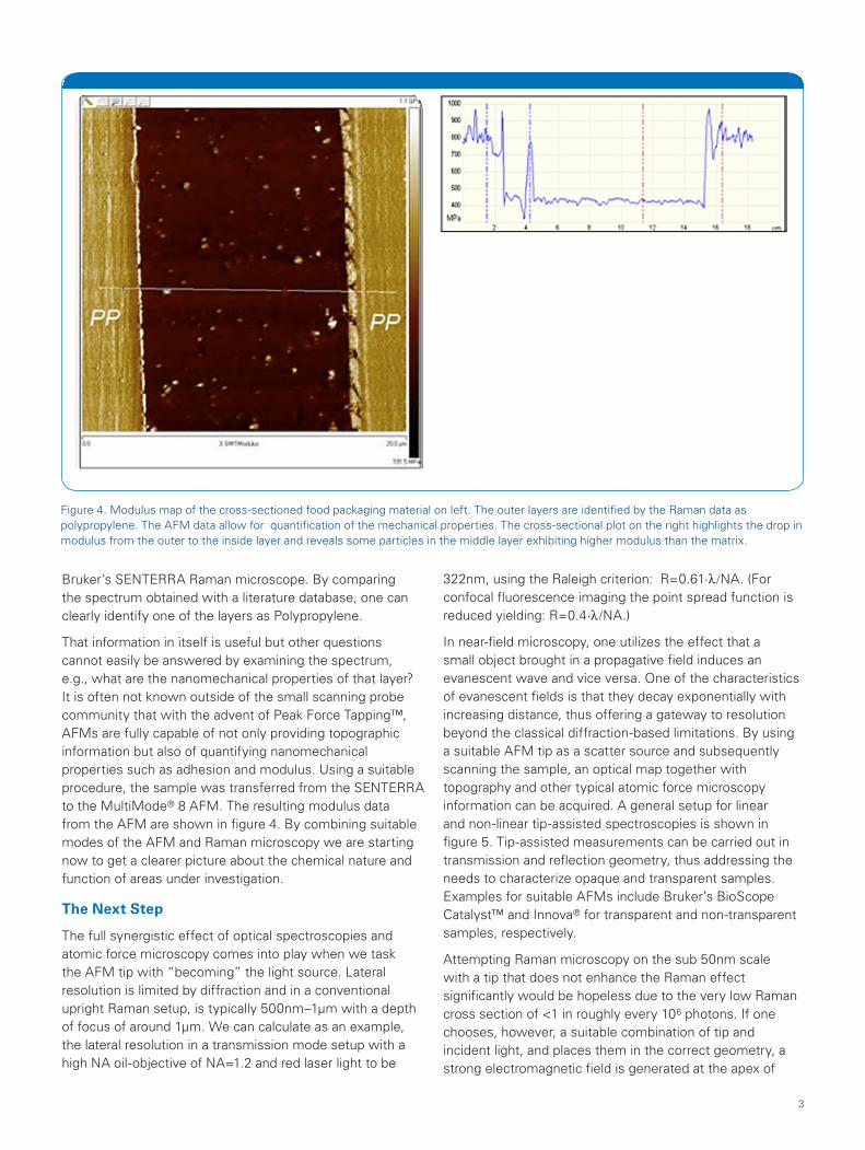
A Raman spectrometer is often combined with an optical microscope to take advantage of the high spatial resolution that a confocal optical setup can offer. The main components of a dispersive Raman setup are a laser illuminating the sample, optics to collect the backscattered radiation, a high efficient laser line rejection filter, and finally a spectrometer consisting of an entrance slit, a diffraction grating and a CCD camera. A basic schematic of a simple Raman spectrometer is shown in figure 2.
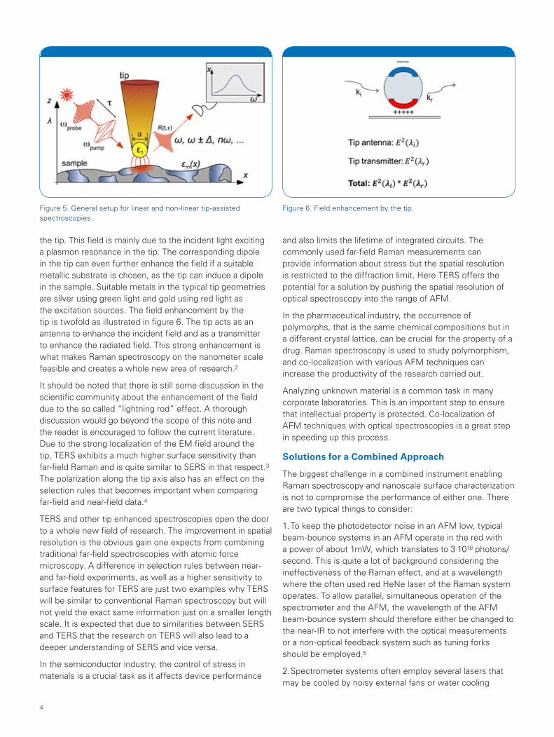
Optical spectroscopies like Raman and atomic force microscopy are of a complementary nature. Each technique often does not provide a sufficient enough picture of the problem by itself but when applied in a co-localized fashion they become quite powerful, i.e., analyzing the same region of a sample. By doing so, not only can the question of what the material in the field of view (FOV) is be answered but also its physical dimensions and properties can be revealed on the nanoscale. The Raman spectrum shown in figure 3 was taken on one of the layers of a cross-sectioned piece of packing material for unfrosted animal crackers using
Raman Spectroscopy
Spectroscopy is the study of the interaction of electromagnetic radiation with matter. The most common kinds are fluorescence, infrared, and Raman.1 The latter two are vibrational techniques, i.e., the energy of radiation they use is sufficient to excite molecular or lattice vibrations. In a Raman experiment, the sample is illuminated with monochromatic light and the inelastic scattered light detected. If a sample is illuminated with light of a frequency ν0 most of the scattered light is Raleigh scattered, i.e. elastically scattered and does not change in frequency. A small portion, however, is at a different frequency ν1 due to a change in the polarizability of the illuminated molecule. This shift is referred to as the Stokes shift if ν1 is red-shifted with regards to the incident light, or anti-Stokes if ν1 is blue-shifted.
Figure 2. Schematic of a Raman spectrometer. The sample is illuminated by a monochromatic light source. After passing through a filter rejecting the laser light it is dispersed by a grating and imaged onto a CCD chip.
2
Figure 3. Spectrum (black) of a layer of food packaging material and literature spectrum for Poly-propylene (red).
Bruker’s SENTERRA Raman microscope. By comparing the spectrum obtained with a literature database, one can clearly identify one of the layers as Polypropylene.
That information in itself is useful but other questions cannot easily be answered by examining the spectrum, e.g., what are the nanomechanical properties of that layer? It is often not known outside of the small scanning probe community that with the advent of Peak Force Tapping™, AFMs are fully capable of not only providing topographic information but also of quantifying nanomechanical properties such as adhesion and modulus. Using a suitable procedure, the sample was transferred from the SENTERRA to the MultiMode® 8 AFM. The resulting modulus data from the AFM are shown in figure 4. By combining suitable modes of the AFM and Raman microscopy we are starting now to get a clearer picture about the chemical nature and function of areas under investigation.
The Next Step
The full synergistic effect of optical spectroscopies and atomic force microscopy comes into play when we task the AFM tip with “becoming” the light source. Lateral resolution is limited by diffraction and in a conventional upright Raman setup, is typically 500nm–1µm with a depth of focus of around 1µm. We can calculate as an example, the lateral resolution in a transmission mode setup with a high NA oil-objective of NA=1.2 and red laser light to be
3
322nm, using the Raleigh criterion: R=0.61∙λ/NA. (For confocal fluorescence imaging the point spread function is reduced yielding: R=0.4∙λ/NA.)
In near-field microscopy, one utilizes the effect that a small object brought in a propagative field induces an evanescent wave and vice versa. One of the characteristics of evanescent fields is that they decay exponentially with increasing distance, thus offering a gateway to resolution beyond the classical diffraction-based limitations. By using a suitable AFM tip as a scatter source and subsequently scanning the sample, an optical map together with topography and other typical atomic force microscopy information can be acquired. A general setup for linear and non-linear tip-assisted spectroscopies is shown in figure 5. Tip-assisted measurements can be carried out in transmission and reflection geometry, thus addressing the needs to characterize opaque and transparent samples. Examples for suitable AFMs include Bruker’s BioScope Catalyst™ and Innova® for transparent and non-transparent samples, respectively.
Attempting Raman microscopy on the sub 50nm scale with a tip that does not enhance the Raman effect significantly would be hopeless due to the very low Raman cross section of <1 in roughly every 106 photons. If one chooses, however, a suitable combination of tip and incident light, and places them in the correct geometry, a strong electromagnetic field is generated at the apex of
Figure 4. Modulus map of the cross-sectioned food packaging material on left. The outer layers are identified by the Raman data as polypropylene. The AFM data allow for quantification of the mechanical properties. The cross-sectional plot on the right highlights the drop in modulus from the outer to the inside layer and reveals some particles in the middle layer exhibiting higher modulus than the matrix.
and also limits the lifetime of integrated circuits. The commonly used far-field Raman measurements can provide information about stress but the spatial resolution is restricted to the diffraction limit. Here TERS offers the potential for a solution by pushing the spatial resolution of optical spectroscopy into the range of AFM.
In the pharmaceutical industry, the occurrence of polymorphs, that is the same chemical compositions but in a different crystal lattice, can be crucial for the property of a drug. Raman spectroscopy is used to study polymorphism, and co-localization with various AFM techniques can increase the productivity of the research carried out.
Analyzing unknown material is a common task in many corporate laboratories. This is an important step to ensure that intellectual property is protected. Co-localization of AFM techniques with optical spectroscopies is a great step in speeding up this process.
Solutions for a Combined Approach
The biggest challenge in a combined instrument enabling Raman spectroscopy and nanoscale surface characterization is not to compromise the performance of either one. There are two typical things to consider:
1. To keep the photodetector noise in an AFM low, typical beam-bounce systems in an AFM operate in the red with a power of about 1mW, which translates to 3∙1018 photons/second. This is quite a lot of background considering the ineffectiveness of the Raman effect, and at a wavelength where the often used red HeNe laser of the Raman system operates. To allow parallel, simultaneous operation of the spectrometer and the AFM, the wavelength of the AFM beam-bounce system should therefore either be changed to the near-IR to not interfere with the optical measurements or a non-optical feedback system such as tuning forks should be employed.5
2. Spectrometer systems often employ several lasers that may be cooled by noisy external fans or water cooling
4
Figure 5. General setup for linear and non-linear tip-assisted spectroscopies.
the tip. This field is mainly due to the incident light exciting a plasmon resonance in the tip. The corresponding dipole in the tip can even further enhance the field if a suitable metallic substrate is chosen, as the tip can induce a dipole in the sample. Suitable metals in the typical tip geometries are silver using green light and gold using red light as the excitation sources. The field enhancement by the tip is twofold as illustrated in figure 6. The tip acts as an antenna to enhance the incident field and as a transmitter to enhance the radiated field. This strong enhancement is what makes Raman spectroscopy on the nanometer scale feasible and creates a whole new area of research.2
It should be noted that there is still some discussion in the scientific community about the enhancement of the field due to the so called “lightning rod” effect. A thorough discussion would go beyond the scope of this note and the reader is encouraged to follow the current literature. Due to the strong localization of the EM field around the tip, TERS exhibits a much higher surface sensitivity than far-field Raman and is quite similar to SERS in that respect.3 The polarization along the tip axis also has an effect on the selection rules that becomes important when comparing far-field and near-field data.4
TERS and other tip enhanced spectroscopies open the door to a whole new field of research. The improvement in spatial resolution is the obvious gain one expects from combining traditional far-field spectroscopies with atomic force microscopy. A difference in selection rules between near-and far-field experiments, as well as a higher sensitivity to surface features for TERS are just two examples why TERS will be similar to conventional Raman spectroscopy but will not yield the exact same information just on a smaller length scale. It is expected that due to similarities between SERS and TERS that the research on TERS will also lead to a deeper understanding of SERS and vice versa.
In the semiconductor industry, the control of stress in materials is a crucial task as it affects device performance
Figure 6. Field enhancement by the tip.
5
systems or radiate quite some heat in the proximity of the AFM. Both of these effects can negatively impact AFM performance. Noise from heating fans can couple into the AFM and cause instabilities in the feedback loop. Temperature changes will cause the AFM to drift and will make it extremely difficult to keep the tip in the selected field-of-view.
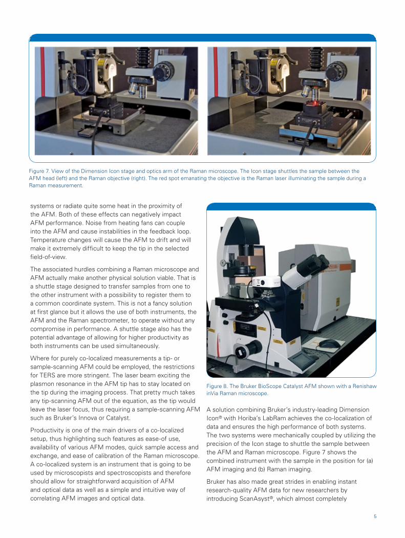
The associated hurdles combining a Raman microscope and AFM actually make another physical solution viable. That is a shuttle stage designed to transfer samples from one to the other instrument with a possibility to register them to a common coordinate system. This is not a fancy solution at first glance but it allows the use of both instruments, the AFM and the Raman spectrometer, to operate without any compromise in performance. A shuttle stage also has the potential advantage of allowing for higher productivity as both instruments can be used simultaneously.
Where for purely co-localized measurements a tip- or sample-scanning AFM could be employed, the restrictions for TERS are more stringent. The laser beam exciting the plasmon resonance in the AFM tip has to stay located on the tip during the imaging process. That pretty much takes any tip-scanning AFM out of the equation, as the tip would leave the laser focus, thus requiring a sample-scanning AFM such as Bruker’s Innova or Catalyst.
Productivity is one of the main drivers of a co-localized setup, thus highlighting such features as ease-of use, availability of various AFM modes, quick sample access and exchange, and ease of calibration of the Raman microscope. A co-localized system is an instrument that is going to be used by microscopists and spectroscopists and therefore should allow for straightforward acquisition of AFM and optical data as well as a simple and intuitive way of correlating AFM images and optical data.
A solution combining Bruker’s industry-leading Dimension Icon® with Horiba’s LabRam achieves the co-localization of data and ensures the high performance of both systems. The two systems were mechanically coupled by utilizing the precision of the Icon stage to shuttle the sample between the AFM and Raman microscope. Figure 7 shows the combined instrument with the sample in the position for (a) AFM imaging and (b) Raman imaging.
Bruker has also made great strides in enabling instant research-quality AFM data for new researchers by introducing ScanAsyst®, which almost completely
Figure 7. View of the Dimension Icon stage and optics arm of the Raman microscope. The Icon stage shuttles the sample between the AFM head (left) and the Raman objective (right). The red spot emanating the objective is the Raman laser illuminating the sample during a Raman measurement.
Figure 8. The Bruker BioScope Catalyst AFM shown with a Renishaw inVia Raman microscope.
compared to the non-aromatic reference line at 1014 cm-1 are lower in the thicker parts of the sample. The Raman map in the middle of figure 9 shows this strikingly. Raman data can provide information about the steric orientation of a sample. Here, the molecules are likely oriented differently in the thick and thinner areas of the sample. The incident polarized laser used might therefore help to highlight the orientation of the aromatic rings on the aluminum substrate.
Example Two
Polymorphism is the ability of a material to exist in more than one crystal structure. This can have profound impacts on its mechanical behavior or physiological impact in the case of drugs, for example. The following example describes a study on Yttria-stabilized zirconia polycrystals (Y-TZP). Y-TZP is often used in dental implants for its biomechanical and esthetic properties. The material is typically sintered from a fine powder and can be crystallized in the tetragonal form. An unwanted phase transformation, however, can take place under certain conditions resulting in a monoclinic lattice.
6
automates AFM operation without scarifying performance.6
The following section discusses some results from co-localized measurements.
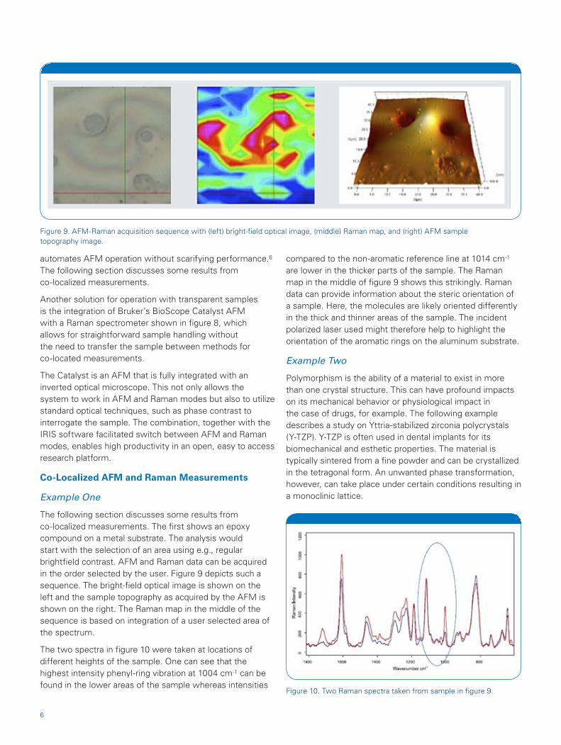
Another solution for operation with transparent samples is the integration of Bruker’s BioScope Catalyst AFM with a Raman spectrometer shown in figure 8, which allows for straightforward sample handling without the need to transfer the sample between methods for co-located measurements.
The Catalyst is an AFM that is fully integrated with an inverted optical microscope. This not only allows the system to work in AFM and Raman modes but also to utilize standard optical techniques, such as phase contrast to interrogate the sample. The combination, together with the IRIS software facilitated switch between AFM and Raman modes, enables high productivity in an open, easy to access research platform.
Co-Localized AFM and Raman Measurements
Example One
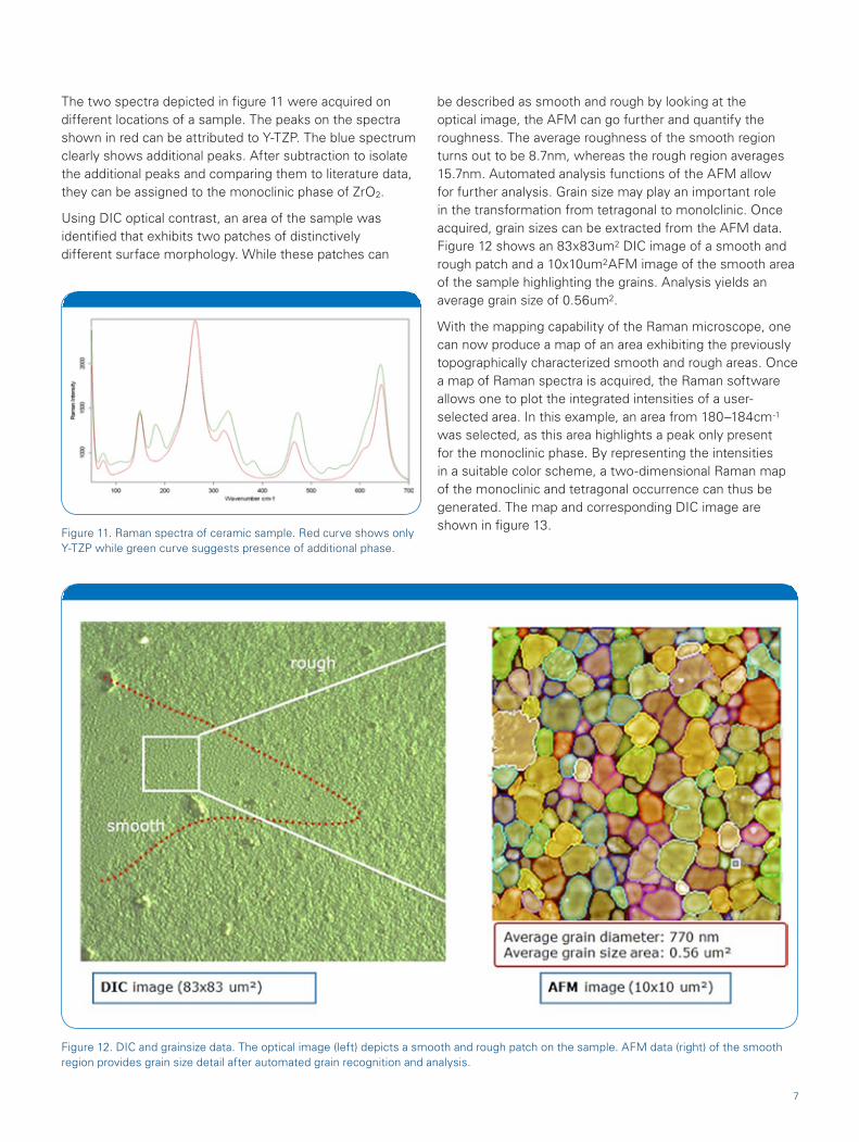
The following section discusses some results from co-localized measurements. The first shows an epoxy compound on a metal substrate. The analysis would start with the selection of an area using e.g., regular brightfield contrast. AFM and Raman data can be acquired in the order selected by the user. Figure 9 depicts such a sequence. The bright-field optical image is shown on the left and the sample topography as acquired by the AFM is shown on the right. The Raman map in the middle of the sequence is based on integration of a user selected area of the spectrum.
The two spectra in figure 10 were taken at locations of different heights of the sample. One can see that the highest intensity phenyl-ring vibration at 1004 cm-1 can be found in the lower areas of the sample whereas intensities
Figure 9. AFM-Raman acquisition sequence with (left) bright-field optical image, (middle) Raman map, and (right) AFM sample topography image.
Figure 10. Two Raman spectra taken from sample in figure 9.
The two spectra depicted in figure 11 were acquired on different locations of a sample. The peaks on the spectra shown in red can be attributed to Y-TZP. The blue spectrum clearly shows additional peaks. After subtraction to isolate the additional peaks and comparing them to literature data, they can be assigned to the monoclinic phase of ZrO2.
Using DIC optical contrast, an area of the sample was identified that exhibits two patches of distinctively different surface morphology. While these patches can
be described as smooth and rough by looking at the optical image, the AFM can go further and quantify the roughness. The average roughness of the smooth region turns out to be 8.7nm, whereas the rough region averages 15.7nm. Automated analysis functions of the AFM allow for further analysis. Grain size may play an important role in the transformation from tetragonal to monolclinic. Once acquired, grain sizes can be extracted from the AFM data. Figure 12 shows an 83x83um2 DIC image of a smooth and rough patch and a 10x10um2AFM image of the smooth area of the sample highlighting the grains. Analysis yields an average grain size of 0.56um2.
With the mapping capability of the Raman microscope, one can now produce a map of an area exhibiting the previously topographically characterized smooth and rough areas. Once a map of Raman spectra is acquired, the Raman software allows one to plot the integrated intensities of a user-selected area. In this example, an area from 180–184cm-1 was selected, as this area highlights a peak only present for the monoclinic phase. By representing the intensities in a suitable color scheme, a two-dimensional Raman map of the monoclinic and tetragonal occurrence can thus be generated. The map and corresponding DIC image are shown in figure 13.
7
Figure 12. DIC and grainsize data. The optical image (left) depicts a smooth and rough patch on the sample. AFM data (right) of the smooth region provides grain size detail after automated grain recognition and analysis.
Figure 11. Raman spectra of ceramic sample. Red curve shows only Y-TZP while green curve suggests presence of additional phase.
nonuniformly over the surface. The use of co-localized AFM, Raman, and DIC microscopy enabled the study of the process on the nanometer scale.
Figure 13. DIC and Raman map.
Figure 14. TERS-ready combination of the Bruker Innova Scanning Probe Microsope and the Renishaw inVia Raman microscope. The optical coupling is achieved via a trackball operated sampling arm.
8
The example of performing a combined AFM and RAMAN analysis of the ceramic sample can be summarized as follows. The monoclinic to tetragonal phase transformation of Y-TZP results in a surface roughening that occurs
A Setup for TERS: Innova IRIS
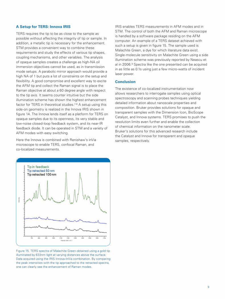
TERS requires the tip to be as close to the sample as possible without affecting the integrity of tip or sample. In addition, a metallic tip is necessary for the enhancement. STM provides a convenient way to combine these requirements and study the effects of various tip shapes, coupling mechanisms, and other variables. The analysis of opaque samples creates a challenge as high-NA oil immersion objectives cannot be used, as in transmission mode setups. A parabolic mirror approach would provide a high NA of 1 but puts a lot of constraints on the setup and flexibility. A good compromise and excellent way to excite the AFM tip and collect the Raman signal is to place the Raman objective at about a 60 degree angle with respect to the tip axis. It seems counter intuitive but the side illumination scheme has shown the highest enhancement factor for TERS in theoretical studies.7-8 A setup using this side-on geometry is realized in the Innova IRIS shown in figure 14. The Innova lends itself as a platform for TERS on opaque samples due to its openness, its very stable and low-noise closed-loop feedback system, and its near-IR feedback diode. It can be operated in STM and a variety of AFM modes with easy switching.
Here the Innova is combined with Renishaw’s inVia microscope to enable TERS, confocal Raman, and co-localized measurements.
IRIS enables TERS measurements in AFM modes and in STM. The control of both the AFM and Raman microscope is handled by a software package residing on the AFM computer. An example of a TERS dataset achieved with such a setup is given in figure 15. The sample used is Malachite Green, a dye for which literature data exist. Single-molecule sensitivity on Malachite Green using a side illumination scheme was previously reported by Neascu et al in 2006.9 Spectra like the one presented can be acquired in as little as 0.1s using just a few micro-watts of incident laser power.
Conclusion
The existence of co-localized instrumentation now allows researchers to interrogate samples using optical spectroscopy and scanning probes techniques yielding detailed information about nanoscale properties and composition. Bruker provides solutions for opaque and transparent samples with the Dimension Icon, BioScope Catalyst, and Innova systems. TERS promises to push the resolution limits even further and enable the collection of chemical information on the nanometer scale. Bruker’s solutions for this advanced research include the Catalyst and Innova for transparent and opaque samples, respectively.
Figure 15. TERS spectra of Malachite Green obtained using a gold tip illuminated by 633nm light at varying distances above the surface. Data acquired using the IRIS Innova-InVia combination. By comparing the peak intensities with the tip approached to the retracted spectra, one can clearly see the enhancement of Raman modes.
9
©20
12 B
ruke
r C
orpo
ratio
n. A
ll rig
hts
rese
rved
. Bio
Sco
pe C
atal
yst,
Dim
ensi
on Ic
on, I
nnov
a, IR
IS, N
anoS
cope
, and
Tap
ping
Mod
e ar
e tr
adem
arks
or
regi
ster
ed t
rade
mar
ks o
f B
ruke
r C
orpo
ratio
n. A
ll ot
her
trad
emar
ks a
re t
he p
rope
rty
of t
heir
resp
ectiv
e co
mpa
nies
. AN
136,
Rev
. A2
Bruker Nano Surfaces Divison
Santa Barbara, CA · USA+1.805.967.1400/[email protected]
www.bruker .com
References
1. H. Kuzmany, Solid State Spectroscopy, 2nd edition (Springer 2009).
2. R. Stöckle, Y.D. Suh, V. Deckert, and R. Zenobi, Chem. Phys. Lett. 318, 131 (2000).
3. T. Ichimura, S. Fujii, and S. Kawata. Phys.Rev. Lett. 102 (2009).
4. C.C. Neacsu, S. Berweger, and M.B. Raschke, Nanobiotechnology 3, 172 (2007).
5. W.H.J. Rensen, Ph.D. thesis, Univ. of Twente (2002).
6. S.B. Kaemmer, Bruker AN133 (2011).
7. A. Downes,D. Salter, and A. Elfick, J. Phys. Chem. B 2006, 110,
8. Z. Yang, J. Aizpurua, and H. Xu, J. Raman Spectrosc. 2009, 40,
9. C.C. Neascu, J. Dreyer, N. Behr, and M.B. Raschke, Physical Review B 73, 193403 (2006).
Author
Stefan Kaemmer, Ph.D., Bruker Nano Surfaces Division ([email protected])
Acknowledgements
YZTP sample courtesy of Dr. Ing. Lubica Hallman (Center of Dental Medicine, University of Zürich).
I would like to acknowledge the help from my colleagues: Ton Ruiter, Ph.D., Natalia Erina, Ph.D., Igor Nemeth, Ph.D., and Tim Batten, Ph.D. (Renishaw).