application note: virtex-5 family bus master dma...
TRANSCRIPT
XAPP1052 (v1.1) August 22, 2008 www.xilinx.com 1
© 2008 Xilinx, Inc. All rights reserved. XILINX, the Xilinx logo, and other designated brands included herein are trademarks of Xilinx, Inc. All other trademarks are the property of their respective owners.
Summary This application note discusses how to design and implement a Bus Master Direct Memory Access (DMA) design for the Endpoint Block Plus Wrapper Core for PCI Express® using the Virtex®-5 FPGA Integrated Block for PCI Express. The Bus Master DMA (BMD) design moves data to and from host memory. Included with the BMD hardware design is a DMA kernel mode driver, including source and Windows 32-bit software application, both provided by Avnet. Instructions for installing both the driver and application are included in this application note.
Note: The BMD hardware design, Avnet DMA driver, and Windows application are provided “as is” with no implied warranty or support.
Overview DMA is a technique used for efficient transfer of data to and from host CPU system memory. DMA implementations have many advantages over standard programmed input/output data transfers. Bus master DMA applications result in higher throughput and performance, as well as lower overall CPU utilization. There are two basic types of DMA applications found in systems using PCI Express. These are a system DMA application and a bus master DMA application. System DMAs are not typical and very few root complexes and OS support their use. A Bus Master DMA application is by far the most common type of DMA found in PCI Express based systems. A bus master DMA is the endpoint device containing the DMA engine that controls moving data to (Memory Writes) or requesting data from (Memory Reads) system memory.
Consider the scenario in which there are 1024 bytes of data residing in system memory that need to be transferred to a peripheral device over the PCI Express link. With a system DMA, the CPU is in control of moving the data through memory writes to the peripheral device. The disadvantage to this approach is that it requires CPU cycles to command the data movement, as well as more buffering in the ports root complex. Alternatively, when a bus master DMA is used, the CPU is not used during the transfer of the data, which means it can perform other processing activities. Through programmed input/output data transfers, the bus master DMA in the device is instructed to move data. The BMD then controls the transfer and reads the data from the system memory moving it from the memory to the device.
Figure 1 shows a typical system architecture that includes a root complex, PCI Express switch device, and a PCI Express endpoint. A DMA transfer either moves data from an endpoint buffer into system memory or from system memory into the endpoint buffer. A memory controller in the root complex controls the transfer of data into system memory, which allows the CPU to perform other operations while the transfer is in progress. The DMA request is always initiated by the endpoint after receiving instructions from the application driver.
Application Note: Virtex-5 Family
XAPP1052 (v1.1) August 22, 2008
Bus Master DMA Reference Design for the Xilinx Endpoint Block Plus Core for PCI ExpressAuthor: Jake Wiltgen
R

Components of a Design for PCI Express
XAPP1052 (v1.1) August 22, 2008 www.xilinx.com 2
R
Memory Write (MWr) transaction layer packets (TLPs) are used to transfer data from an endpoint buffer into main memory via the memory controller. A requestor-completion model is used when transferring data from main memory to the endpoint. Memory Read (MRd) TLPs are sent from the endpoint to the memory controller, which contains a specified address and byte count.
The two methods listed above require initial operational information before initiating the transfer. This information is typically provided using programmed input/output memory writes generated by system software. The required information consists of the memory address and amount of data to be transferred. In either flow, the endpoint initiates the transfer and signals the end of a transfer by generating an interrupt up to the device driver.
Components of a Design for PCI Express
A typical design for PCI Express includes the following main components:
• Hardware HDL Design
• Driver Design
• Software Application
The hardware design refers to the Verilog or VHDL application residing on the Xilinx® FPGA. In this case, it is the bus master DMA design or BMD. This design contains control engines for the receive and transmit data path along with various registers and memory interfaces to store and retrieve data. The BMD is explained in more detail in “Exploring the Bus Master Design,” page 5.
X-Ref Target - Figure 1
Figure 1: System Architecture
CPU
PCIeRoot Complex
PCI Bus 0
PCI Bus 1
PCI Bus x
X1052_01_012508
MemoryController
Device
MainMemory
PCIeRoot Port
PCIeSwitch
PCIeEndpoint
Exploring the DMA Performance Demo Hierarchy
XAPP1052 (v1.1) August 22, 2008 www.xilinx.com 3
R
The driver design is normally written in C and is the link between the higher level software application and the hardware application. The driver contains various routines that are called by the software application and are used to communicate with the hardware via the PCI Express link. The driver resides in the kernel memory on the system.
The software application is most apparent to the user, and can be written in any programming language. It can be as simple as a small C program or as complex as a GUI-based application. The user interfaces with the software application, which invokes routines in the driver to perform the necessary data movements. Once completed, the hardware issues an interrupt informing the driver that the data movement is finished. Then, the driver can invoke routines in the software application to inform you that the request is completed.
Exploring the DMA Performance Demo Hierarchy
The BMD Performance Demonstration Design is used by Xilinx to test core functionality and gather performance information. Customers can use this design to measure performance on their own system. To test performance, the BMD design fabricates the data payload using a pre-determined data pattern defined in a backend control register. Counters and registers are also implemented to measure link performance.
Extract the pcie_performance_demo.zip file to the same level as the core netlist. The top-level directory is named dma_performance_demo and subdirectories are defined in the following sections.
• dma_performance_demo
Top-level directory for the DMA reference design
♦ fpga
- BMD
Bus Master Design RTL source code
- Implementation
Implementation scripts to build Bus Master Design
♦ Driver
Driver install files pcie_demo.sys and oemsetupXP.inf files
- Source
Driver source files to compile and build driver
♦ win32_application
DMA Windows application install executable
dma_performance_demo/driver
The driver directory contains the driver installation files.
Table 1: Driver Directory
Name Description
dma_performance_demo/driver
oemsetupXP.inf Windows setup information file
pcie_demo.sys Windows device driver
Exploring the DMA Performance Demo Hierarchy
XAPP1052 (v1.1) August 22, 2008 www.xilinx.com 4
R
dma_performance_demo/driver/source
The source directory contains the DMA driver source files.
dma_performance_demo/fpga/BMD/rtl
The rtl directory contains the Bus Master Application source code.
Table 2: Source Directory
Name Description
dma_performance_demo/driver/source
build.cmdsourcesMakefileMakefile.inc
DOS build scripts
pnp.c Driver source implementing Plug and Play functionality
s3_1000cs3_1000.hs3_1000.rcioctrl_h
Device specific driver source code
msglog.hMsglog.mcMSG0001.bin
Windows event logging source code
Table 3: RTL Directory
Name Description
dma_performance_demo/fpga/bmd/rtl
BMD.vBMD_32.vBMD_32_RX_ENGINE.vBMD_32_TX_ENGINE.vBMD_64.vBMD_64_RX_ENGINE.vBMD_64_TX_ENGINE.vBMD_CFG_CTRL.vBMD_EP.vBMD_EP_MEM.vBMD_EP_MEM_ACCESS.vBMD_INTR_CTRL.vBMD_INTR_CTRL_DELAY.vBMD_RD_THROTTLE.vBMD_TO_CTRL.vpci_exp_64b_app.vpcie_endpoint_product.v
Bus Master Design source files
Exploring the Bus Master Design
XAPP1052 (v1.1) August 22, 2008 www.xilinx.com 5
R
dma_performance_demo/fpga/implement
The implement directory contains the design implementation scripts.
dma_performance_demo/win_32_application
The win_32_application directory contains Windows application installer files.
Exploring the Bus Master Design
The BMD architecture is shown in Figure 2 and consists of initiator logic, target logic, status/control registers, interface logic, and the endpoint core for PCI Express.
Table 4: Implement Directory
Name Description
dma_performance_demo/fpga/implement
implement.bat DOS implementation script
xilinx_pci_exp_1_lane_ep_inc.xstxilinx_pci_exp_4_lane_ep_inc.xstxilinx_pci_exp_8_lane_ep_inc.xst
XST project file for 1-lane, 4-lane, and 8-lane Bus Master design, respectively.
xst.scr XST synthesis script
Table 5: Implement Directory
Name Description
dma_performance_demo/win_32_application
setup.exe Installer executable
PCIe_Perf.CAB Contains application library files
SETUP.LST Packing list file
X-Ref Target - Figure 2
Figure 2: Bus Master Validation Design ArchitectureX1052_02_012508
PCIe Endpoint Core
Interface
Target
WR
ITE
TLP
s
CO
MP
LET
ION
TLP
s
CO
MP
LET
ION
TLP
s
RE
AD
/WR
ITE
TLP
s
READ TLPs
Initiator Logic
Control/Status RegistersRx Tx
PC
Ie
Exploring the Bus Master Design
XAPP1052 (v1.1) August 22, 2008 www.xilinx.com 6
R
Target Logic
Target logic is responsible for capturing single Dword Memory Write (MWr) and Memory Read (MRd) TLPs presented on the interface. MWr and MRd TLPs are sent to the endpoint via Programmed Input/Output and are used to monitor and control the DMA hardware. The function of the target logic is to update the status and control registers during MWr’s and return Completions with Data for all incoming MRd’s. All incoming MWr packets are 32-bit and contain a one Dword (32-bits) payload. Incoming MRd packets should only request 1 Dword of data at a time resulting in Completions with Data of a single Dword.
Control and Status Registers
The control and status registers contain operational information for the DMA controller. It is important to note that the example BMD design provided is primarily used to measure performance of data transfers and, consequently, contains status registers that may not be needed in typical designs. You can choose to remove these and their associated logic if needed. All registers are defined in “Appendix A.”
Initiator Logic
The function of the initiator block is to generate Memory Write or Memory Read TLPs depending on whether an upstream or downstream transfer is selected. The Bus Master Design only supports generating one type of a data flow at a single time. The Bus Master Enable bit (Bit 2 of PCI Command Register) must be set to initiate TLP traffic upstream. No transactions are allowed to cross the 4K boundary.
The initiator logic generates Memory Write TLPs when transferring data from the endpoint to system memory. The Write DMA control and status registers specify the address, size, payload content, and number of TLPs to be sent.
The first TLP contains the start address, which is specified in the Write DMA TLP Address (WDMATLPA; see “Appendix A”) register. Subsequent TLPs contain an address that is a function of the address stored in WDMATLPA plus the TLP size defined in the Write DMA TLP Size (WDMATLPS) register. The initiator sends Memory Writes with a specific data pattern. Each DWORD in the payload contains the contents of the Write DMA Data Pattern register (WDMATLPP). Note that in a normal application, the data would consist of information in the device being moved to the host memory; however, for the example reference design it is a set pattern found in the WDMATLPP register.
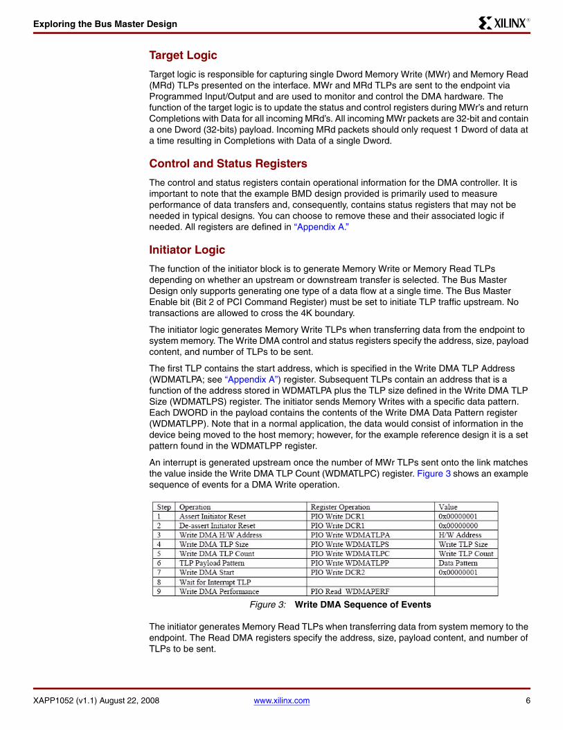
An interrupt is generated upstream once the number of MWr TLPs sent onto the link matches the value inside the Write DMA TLP Count (WDMATLPC) register. Figure 3 shows an example sequence of events for a DMA Write operation.
The initiator generates Memory Read TLPs when transferring data from system memory to the endpoint. The Read DMA registers specify the address, size, payload content, and number of TLPs to be sent.
X-Ref Target - Figure 3
Figure 3: Write DMA Sequence of Events

Setting Up the BMD Design
XAPP1052 (v1.1) August 22, 2008 www.xilinx.com 7
R
The first TLP address is specified by the Read DMA TLP Address (WDMATLPA) register. Each additional TLP in the transfer contains an address that is a function of WDMATLPA plus the TLP size defined in the Read DMA TLP Size (WDMATLPS) register. The TLP tag number starts at zero and is incremented by one for each additional TLP, guaranteeing a unique number for each packet. Completions with Data are expected to be received in response to the Memory Read Request packets. Initiator logic tracks incoming completions and calculates a running total of the amount of data received. Once the requested data size has been received, the endpoint generates an interrupt TLP upstream to indicate the end of the DMA transfer. Additional error checking is performed inside the initiator. Each DWORD inside a Completion payload must match the value in the Read DMA TLP Pattern (RDMATLPP) register. The total payload returned must also equal Read DMA TLP Count times Read DMA TLP Size (RDMATLPC and RDMATLPS, respectively). Figure 4 shows an example sequence of events for a DMA Read operation.
The type of interrupt TLP generated in both cases is controllable via the PCI Command Register’s interrupt Disable bit and/or the MSI Enable bit within the MSI capability structure. When the MSI Enable bit is set, the endpoint core generates a MSI request by sending a MWr TLP. If disabled, the endpoint core generates a legacy interrupt as long as Bit 10 of the PCI Command register has interrupts enabled.
The data returned for the Memory Read request is discarded by the BMD application since the application is only concerned with the data movement process. Normally, this data would need to be checked for correct order and then loaded into some type of storage element such as a Block RAM or FIFO.
Setting Up the BMD Design
The Bus Master Design connects up to the transaction (TRN) interface of the Endpoint Block Plus for PCI Express. The TRN interface is described in detail in the UG341, LogiCORE™ IP Endpoint Block Plus for PCI Express User Guide.
Generating the Core
To generate the core, follow these steps:
1. Ensure the latest Xilinx Software along with applicable IP Updates and patches for the core are installed. The latest IP Update is located at:
www.xilinx.com/support/download/index.htm
2. Start the CORE Generator™ software and create a new project.
3. Target a Virtex-5 device that supports the LogiCORE Endpoint Block Plus.
4. In the taxonomy tree, select Standard Bus Interface > PCI Express.
5. Select Endpoint Block Plus and select Customize.
6. On page 2, set the subclass to 80 specifying Other Memory Controller.
7. Page 3 configures the BAR settings for the Endpoint. Configure BAR0 to be a 64-bit memory BAR with a 1KB aperture. BAR1 – BAR5 should be disabled.
8. Leave all other settings at their defaults and click Finish to generate the core.
X-Ref Target - Figure 4
Figure 4: Read DMA Sequence of Events

Building DMA Driver for Windows XP
XAPP1052 (v1.1) August 22, 2008 www.xilinx.com 8
R
Implementing the Bus Master Design
To implement the design, follow these steps:
1. Extract the pcie_performance_demo.zip file to the same level as the core netlist. A directory called dma_performance_demo_x1/4/8 will be added to the core hierarchy as shown in Figure 5.
2. Navigate to the following directory:
dma_performance_demo/fpga/implement
3. Double-click on the implement_dma.bat script provided.
The BMD example is synthesized and implemented. A results directory is created containing a routed.bit file, which is downloaded to the board. Note that the implementation script may need to be modified to point to the correct UCF file for the board being used.
Programming the Board
For a system to recognize an add-in card for PCI Express, the card must be present during bus enumeration, which is performed by the BIOS during the boot process. For this reason, the FPGA must be programmed in one of two ways:
• Using an on-board PROM so that when the system is powered on the FPGA is programmed and enumerated by the BIOS.
• Through the JTAG interface after the OS has started. However, a warm reset must be performed for the card to be recognized. In Windows, this equates to performing a restart.
Note: Re-programming the FPGA after the OS has started may result in the system hanging.
Building DMA Driver for Windows XP
This section explains how to build the DMA device driver using the Windows DDK build environment. Windows DDK tools can be downloaded at: http://www.microsoft.com/whdc/devtools/ddk/default.mspx
After installing Windows DDK, follow the steps to build the DMA device driver.
1. From the start menu navigate to:
All Programs > Development Kits > Windows DDK 3790.1830 > Build Environments > Windows XP > Windows XP Free Build Environment
A DOS prompt appears that represents the Windows DDK build environment.
2. In the DOS prompt, navigate to:
dma_performance_demo/driver/source
3. Enter build in the command prompt to build the driver.
X-Ref Target - Figure 5
Figure 5: Design Top Level Hierarchy

Using DMA Driver for Windows XP
XAPP1052 (v1.1) August 22, 2008 www.xilinx.com 9
R
When the driver is built, the console output specifies that four files were compiled and one executable was built, as shown below in Figure 6.
The output driver file is named pcie_demo.sys and located at:
dma_performance_demo/driver/source/objfre_wxp_x86/i386
Using DMA Driver for Windows XP
The device driver and corresponding installation file are located in dma_performance_demo /driver. The information in the oemsetupXP.inf file is used by the Windows Hardware Wizard to bind the driver to the Device Vendor and Device ID. Each time the system is booted, each device is enumerated and bound to a specific driver, based on the Vendor and Device IDs. When a match is found, the driver is automatically loaded using the Plug and Play interface.
DMA Driver Features
The DMA driver implements the following features:
• Plug and play compatibility
• Packet driven DMA using Map Registers
• Separate read and write adapters to facilitate full-duplex operation
• Queue lists for I/O request packets (IRP’s) that arrive during an in-process transfer. (Not implemented by GUI application)
• Interrupt-capable, including ISR registration and Deferred Procedure Call processing
• Direct I/O to extend the default System Buffering of IRPs
• Hooks for extending the driver for transfers larger than the size of the available map registers
DMA Driver Limitations• Transfer size limited to size of map registers. Typically map registers are 32KB on Intel
chip sets.
• Legacy Interrupt Support only
Installing the Driver
When the card with the BMD design is first installed, Windows attempts to locate the appropriate driver for the device. Windows attempts to match the cards Device ID and Vendor ID to the correct driver. Normally, Windows does not find a matching driver and a New Hardware Wizard is launched. In this scenario, proceed to step 5 below. Occasionally, the operating system associates a standard memory controller to a card and it will need to be replaced, as described below.
1. From the start menu, select Control Panel > Administrative Tools > Computer Management.
2. Select Device Manager.
3. Navigate to the entry representing your PCI Express device.
4. Right click and select Update Driver.
The Hardware Update Wizard window opens.
X-Ref Target - Figure 6
Figure 6: DDK Free Build Environment Console Output
Using DMA Driver for Windows XP
XAPP1052 (v1.1) August 22, 2008 www.xilinx.com 10
R
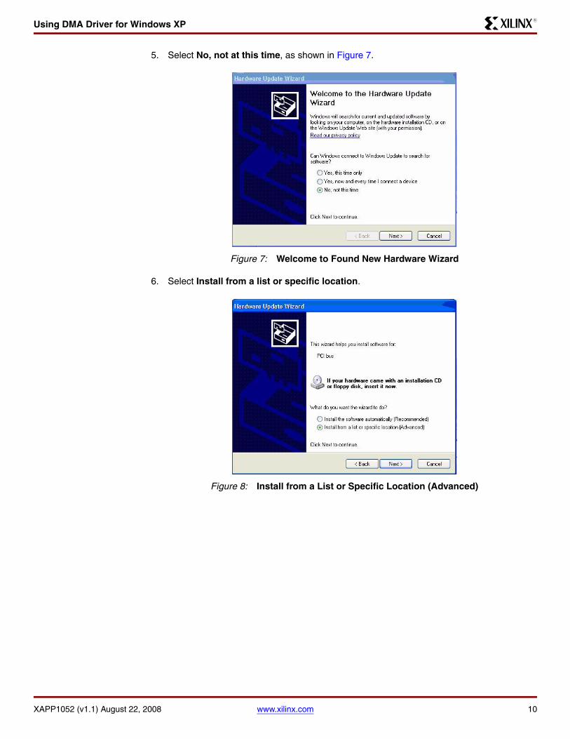
5. Select No, not at this time, as shown in Figure 7.
6. Select Install from a list or specific location.
X-Ref Target - Figure 7
Figure 7: Welcome to Found New Hardware Wizard
X-Ref Target - Figure 8
Figure 8: Install from a List or Specific Location (Advanced)
Using DMA Driver for Windows XP
XAPP1052 (v1.1) August 22, 2008 www.xilinx.com 11
R
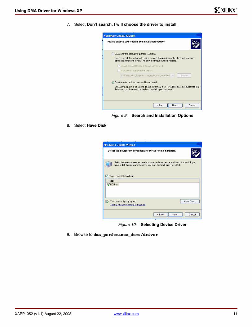
7. Select Don’t search. I will choose the driver to install.
8. Select Have Disk.
9. Browse to dma_perfomance_demo/driver
X-Ref Target - Figure 9
Figure 9: Search and Installation Options
X-Ref Target - Figure 10
Figure 10: Selecting Device Driver

Installing DMA Windows Application for Windows XP
XAPP1052 (v1.1) August 22, 2008 www.xilinx.com 12
R
10. Select oemsetup.inf.
11. Click Open and then OK to return the hardware wizard dialog box.
12. Click Next.
13. Click Finish to complete the installation. Your software is now ready to use with the PCI Express device.
Installing DMA Windows Application for Windows XP
The steps below describe how to install the GUI application.
1. Navigate to dma_performance_demo/win32_application.
2. Run the setup.exe to install the application.
3. After installing the application, a new entry will exist in the Start > All Programs.
Using DMA Application on Windows XP
The software application is a three-tier layered design:
• GUI – provides mouse driven interface to communicate with the driver manager.
• Driver Manager – Controls the GUI application and provides the connection between the GUI and lower level driver. Receives commands from the GUI and generates Windows API calls to the device driver. Driver manager also allocates and retains data buffers in user space.
• Driver – Kernel Mode device driver that follows the standard Windows Development Model to interact with HW.
To launch the GUI, from the Windows Start menu select:
All Programs > Xilinx > Performance Demo for PCIe
X-Ref Target - Figure 11
Figure 11: Locate Device Driver
Using DMA Application on Windows XP
XAPP1052 (v1.1) August 22, 2008 www.xilinx.com 13
R
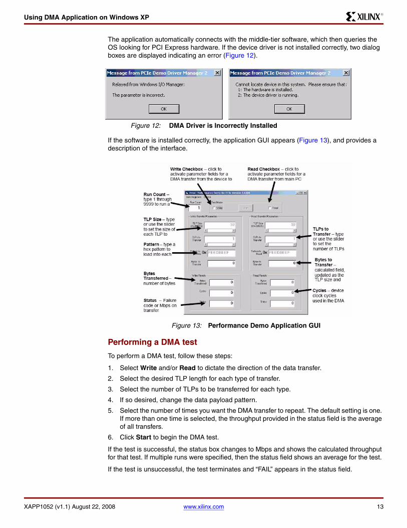
The application automatically connects with the middle-tier software, which then queries the OS looking for PCI Express hardware. If the device driver is not installed correctly, two dialog boxes are displayed indicating an error (Figure 12).
If the software is installed correctly, the application GUI appears (Figure 13), and provides a description of the interface.
Performing a DMA test
To perform a DMA test, follow these steps:
1. Select Write and/or Read to dictate the direction of the data transfer.
2. Select the desired TLP length for each type of transfer.
3. Select the number of TLPs to be transferred for each type.
4. If so desired, change the data payload pattern.
5. Select the number of times you want the DMA transfer to repeat. The default setting is one. If more than one time is selected, the throughput provided in the status field is the average of all transfers.
6. Click Start to begin the DMA test.
If the test is successful, the status box changes to Mbps and shows the calculated throughput for that test. If multiple runs were specified, then the status field shows an average for the test.
If the test is unsuccessful, the test terminates and “FAIL” appears in the status field.
X-Ref Target - Figure 12
Figure 12: DMA Driver is Incorrectly Installed
X-Ref Target - Figure 13
Figure 13: Performance Demo Application GUI
Using DMA Application on Windows XP
XAPP1052 (v1.1) August 22, 2008 www.xilinx.com 14
R
In the unlikely scenario where zero cycles are read in a successful transfer, the calculated transfer rate is infinite. This is an error condition and the word “WOW” is output to the status field.
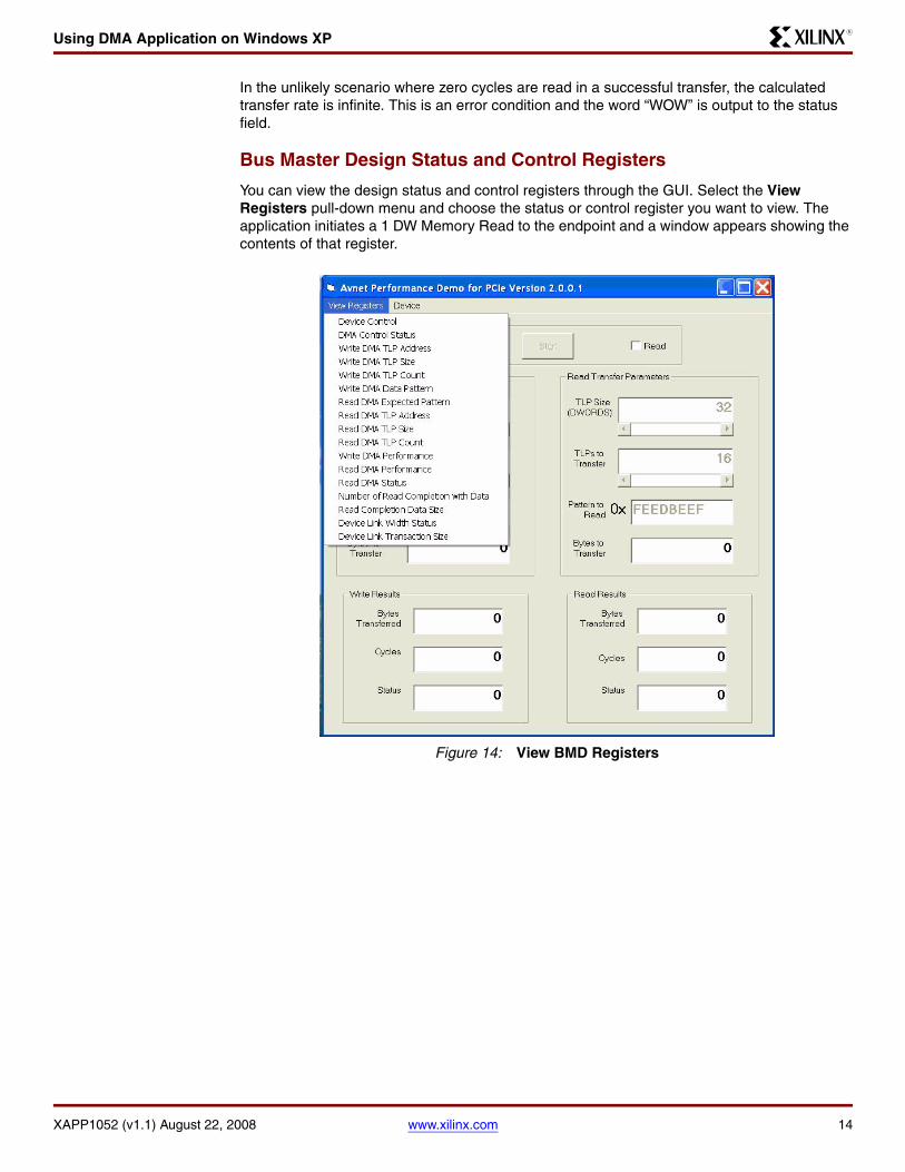
Bus Master Design Status and Control Registers
You can view the design status and control registers through the GUI. Select the View Registers pull-down menu and choose the status or control register you want to view. The application initiates a 1 DW Memory Read to the endpoint and a window appears showing the contents of that register. X-Ref Target - Figure 14
Figure 14: View BMD Registers
Using DMA Application on Windows XP
XAPP1052 (v1.1) August 22, 2008 www.xilinx.com 15
R
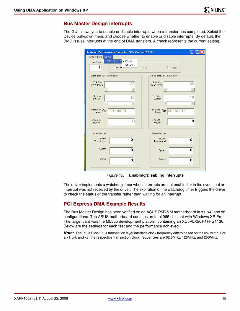
Bus Master Design interrupts
The GUI allows you to enable or disable interrupts when a transfer has completed. Select the Device pull-down menu and choose whether to enable or disable interrupts. By default, the BMD issues interrupts at the end of DMA transfers. A check represents the current setting.
The driver implements a watchdog timer when interrupts are not enabled or in the event that an interrupt was not received by the driver. The expiration of the watchdog timer triggers the driver to check the status of the transfer rather than waiting for an interrupt.
PCI Express DMA Example Results
The Bus Master Design has been verified on an ASUS P5B-VM motherboard in x1, x4, and x8 configurations. The ASUS motherboard contains an Intel 965 chip set with Windows XP Pro. The target card was the ML555 development platform containing an XC5VLX50T-1FFG1136. Below are the settings for each test and the performance achieved.
Note: The PCIe Block Plus transaction layer interface clock frequency differs based on the link width. For a x1, x4, and x8, the respective transaction clock frequencies are 62.5MHz, 125MHz, and 250MHz.
X-Ref Target - Figure 15
Figure 15: Enabling/Disabling Interrupts
Using DMA Application on Windows XP
XAPP1052 (v1.1) August 22, 2008 www.xilinx.com 16
R
GUI Settings (for Both Write and Read Modes)
• Run Count = 1
• TLP Size = 32 DWORDS
• TLPs to Transfer = 256 TLPS
• TLP Pattern = FEEDBEEF
• Bytes to Transfer = 32768
Performance measurements were also taken on a Dell Power Edge 1900 in the x1, x4, and x8 configurations. The Power Edge 1900 contains the Intel E5000P chipset with maximum write payloads of 128 bytes and completion payloads of 64 bytes.
GUI Settings (for Both Write and Read Modes)• Run Count = 1
• TLP Size = 32 DWORDS
• TLPs to Transfer = 256 TLPS
• TLP Pattern = FEEDBEEF
• Bytes to Transfer = 32768
Performance results vary from machine to machine and results can depend upon a number of factors. CPU utilization, peripheral traffic, Root Complex efficiency, and system software all contribute to system performance. When measuring throughput, the PCI Express endpoint is only one element that affects throughput of a PCI Express system.
Table 6: DMA Performance Demo Results
Link Width Performance
Write Read
Bytes Transferred
Throughput Mbps
Bytes Transferred
Throughput Mbps
X1 32768 892 32768 692
X4 32768 6562 32768 4063
X8 32768 10543 32768 9142
Table 7: DMA Performance Demo Results
Link Width Performance
Write Read
Bytes Transferred
Throughput Mbps
Bytes Transferred
Throughput Mbps
X1 32768 1776 32768 1312
X4 32768 6912 32768 5440
X8 32768 14136 32768 10960
Using DMA Application on Windows XP
XAPP1052 (v1.1) August 22, 2008 www.xilinx.com 17
R
PCI Express DMA Example and ChipScope
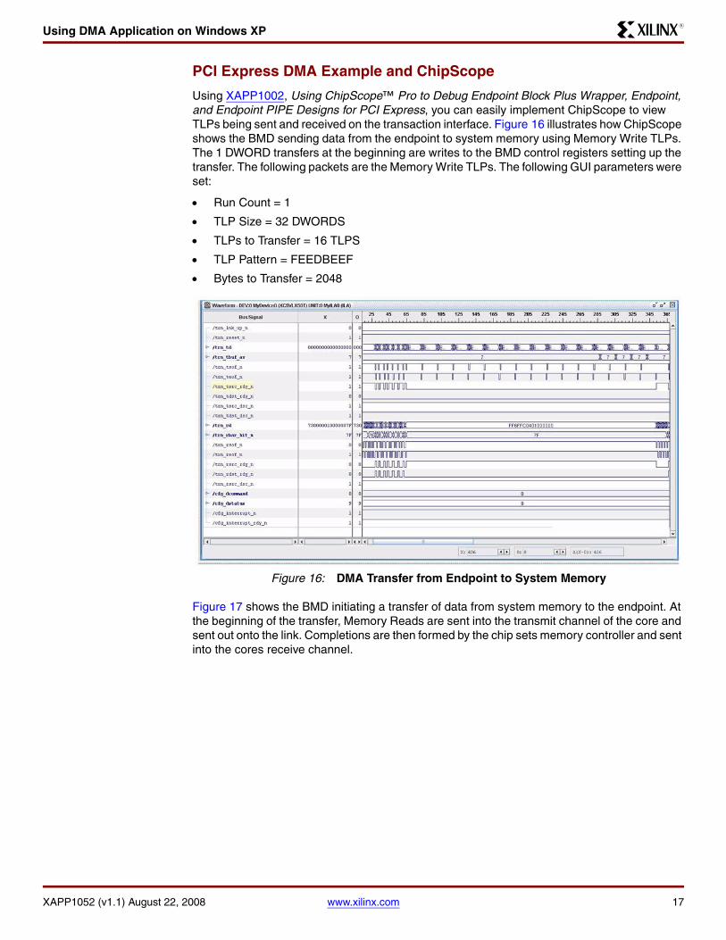
Using XAPP1002, Using ChipScope™ Pro to Debug Endpoint Block Plus Wrapper, Endpoint, and Endpoint PIPE Designs for PCI Express, you can easily implement ChipScope to view TLPs being sent and received on the transaction interface. Figure 16 illustrates how ChipScope shows the BMD sending data from the endpoint to system memory using Memory Write TLPs. The 1 DWORD transfers at the beginning are writes to the BMD control registers setting up the transfer. The following packets are the Memory Write TLPs. The following GUI parameters were set:
• Run Count = 1
• TLP Size = 32 DWORDS
• TLPs to Transfer = 16 TLPS
• TLP Pattern = FEEDBEEF
• Bytes to Transfer = 2048
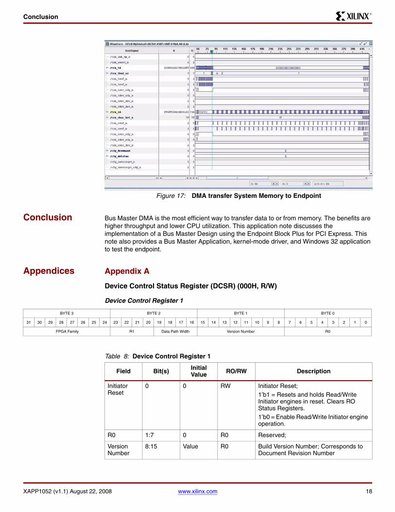
Figure 17 shows the BMD initiating a transfer of data from system memory to the endpoint. At the beginning of the transfer, Memory Reads are sent into the transmit channel of the core and sent out onto the link. Completions are then formed by the chip sets memory controller and sent into the cores receive channel.
X-Ref Target - Figure 16
Figure 16: DMA Transfer from Endpoint to System Memory
Conclusion
XAPP1052 (v1.1) August 22, 2008 www.xilinx.com 18
R
Conclusion Bus Master DMA is the most efficient way to transfer data to or from memory. The benefits are higher throughput and lower CPU utilization. This application note discusses the implementation of a Bus Master Design using the Endpoint Block Plus for PCI Express. This note also provides a Bus Master Application, kernel-mode driver, and Windows 32 application to test the endpoint.
Appendices Appendix A
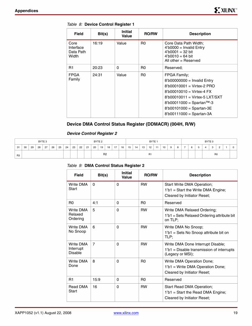
Device Control Status Register (DCSR) (000H, R/W)
Device Control Register 1
X-Ref Target - Figure 17
Figure 17: DMA transfer System Memory to Endpoint
BYTE 3 BYTE 2 BYTE 1 BYTE 0
31 30 29 28 27 26 25 24 23 22 21 20 19 18 17 16 15 14 13 12 11 10 9 8 7 6 5 4 3 2 1 0
FPGA Family R1 Data Path Width Version Number R0
Table 8: Device Control Register 1
Field Bit(s) Initial Value RO/RW Description
Initiator Reset
0 0 RW Initiator Reset;1’b1 = Resets and holds Read/Write Initiator engines in reset. Clears RO Status Registers.1’b0 = Enable Read/Write Initiator engine operation.
R0 1:7 0 R0 Reserved;
Version Number
8:15 Value R0 Build Version Number; Corresponds to Document Revision Number
Appendices
XAPP1052 (v1.1) August 22, 2008 www.xilinx.com 19
R
Device DMA Control Status Register (DDMACR) (004H, R/W)
Device Control Register 2
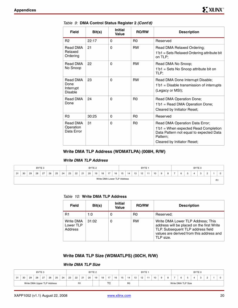
Core Interface Data Path Width
16:19 Value R0 Core Data Path Width;4’b0000 = Invalid Entry4’b0001 = 32 bit4’b0010 = 64 bitAll other = Reserved
R1 20:23 0 R0 Reserved;
FPGA Family
24:31 Value R0 FPGA Family;8’b00000000 = Invalid Entry8’b00010001 = Virtex-2 PRO8’b00010010 = Virtex-4 FX8’b00010011 = Virtex-5 LXT/SXT8’b00011000 = Spartan™-38’b00101000 = Spartan-3E8’b00111000 = Spartan-3A
Table 8: Device Control Register 1
Field Bit(s) Initial Value RO/RW Description
BYTE 3 BYTE 2 BYTE 1 BYTE 0
31 30 29 28 27 26 25 24 23 22 21 20 19 18 17 16 15 14 13 12 11 10 9 8 7 6 5 4 3 2 1 0
R3 R2 R1 R0
Table 9: DMA Control Status Register 2
Field Bit(s) Initial Value RO/RW Description
Write DMA Start
0 0 RW Start Write DMA Operation;1’b1 = Start the Write DMA Engine;Cleared by Initiator Reset;
R0 4:1 0 R0 Reserved
Write DMA Relaxed Ordering
5 0 RW Write DMA Relaxed Ordering;1’b1 = Sets Relaxed Ordering attribute bit on TLP;
Write DMA No Snoop
6 0 RW Write DMA No Snoop;1’b1 = Sets No Snoop attribute bit on TLP;
Write DMA Interrupt Disable
7 0 RW Write DMA Done Interrupt Disable;1’b1 = Disable transmission of interrupts (Legacy or MSI);
Write DMA Done
8 0 R0 Write DMA Operation Done;1’b1 = Write DMA Operation Done;Cleared by Initiator Reset;
R1 15:9 0 R0 Reserved
Read DMA Start
16 0 RW Start Read DMA Operation;1’b1 = Start the Read DMA Engine;Cleared by Initiator Reset;
Appendices
XAPP1052 (v1.1) August 22, 2008 www.xilinx.com 20
R
Write DMA TLP Address (WDMATLPA) (008H, R/W)
Write DMA TLP Address
Write DMA TLP Size (WDMATLPS) (00CH, R/W)
Write DMA TLP Size
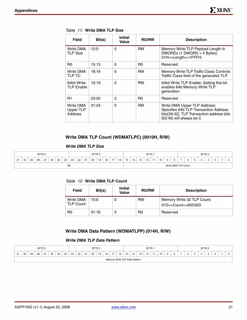
R2 22:17 0 R0 Reserved
Read DMA Relaxed Ordering
21 0 RW Read DMA Relaxed Ordering;1’b1 = Sets Relaxed Ordering attribute bit on TLP;
Read DMA No Snoop
22 0 RW Read DMA No Snoop;1’b1 = Sets No Snoop attribute bit on TLP;
Read DMA Done Interrupt Disable
23 0 RW Read DMA Done Interrupt Disable;1’b1 = Disable transmission of interrupts(Legacy or MSI);
Read DMA Done
24 0 R0 Read DMA Operation Done;1’b1 = Read DMA Operation Done;Cleared by Initiator Reset;
R3 30:25 0 R0 Reserved
Read DMA Operation Data Error
31 0 R0 Read DMA Operation Data Error;1’b1 = When expected Read Completion Data Pattern not equal to expected Data Pattern;Cleared by Initiator Reset;
Table 9: DMA Control Status Register 2 (Cont’d)
Field Bit(s) Initial Value RO/RW Description
BYTE 3 BYTE 2 BYTE 1 BYTE 0
31 30 29 28 27 26 25 24 23 22 21 20 19 18 17 16 15 14 13 12 11 10 9 8 7 6 5 4 3 2 1 0
Write DMA Lower TLP AddressR1
Table 10: Write DMA TLP Address
Field Bit(s) Initial Value RO/RW Description
R1 1:0 0 R0 Reserved;
Write DMA Lower TLP Address
31:02 0 RW Write DMA Lower TLP Address; This address will be placed on the first Write TLP. Subsequent TLP address field values are derived from this address and TLP size.
BYTE 3 BYTE 2 BYTE 1 BYTE 0
31 30 29 28 27 26 25 24 23 22 21 20 19 18 17 16 15 14 13 12 11 10 9 8 7 6 5 4 3 2 1 0
Write DMA Upper TLP Address R1 TC R0 Write DMA TLP Size
Appendices
XAPP1052 (v1.1) August 22, 2008 www.xilinx.com 21
R
Write DMA TLP Count (WDMATLPC) (0010H, R/W)
Write DMA TLP Size
Write DMA Data Pattern (WDMATLPP) (014H, R/W)
Write DMA TLP Data Pattern
Table 11: Write DMA TLP Size
Field Bit(s) Initial Value RO/RW Description
Write DMA TLP Size
12:0 0 RW Memory Write TLP Payload Length in DWORDs (1 DWORD = 4 Bytes); 01H<=Length<=1FFFH;
R0 15:13 0 R0 Reserved
Write DMA TLP TC
18:16 0 RW Memory Write TLP Traffic Class; Controls Traffic Class field of the generated TLP.
64bit Write TLP Enable
19:19 0 RW 64bit Write TLP Enable; Setting this bit enables 64b Memory Write TLP generation.
R1 23:20 0 R0 Reserved
Write DMA Upper TLP Address
31:24 0 RW Write DMA Upper TLP Address; Specifies 64b TLP Transaction Address bits[39:32]. TLP Transaction address bits [63:40] will always be 0.
BYTE 3 BYTE 2 BYTE 1 BYTE 0
31 30 29 28 27 26 25 24 23 22 21 20 19 18 17 16 15 14 13 12 11 10 9 8 7 6 5 4 3 2 1 0
R0 Write DMA TLP Count
Table 12: Write DMA TLP Count
Field Bit(s) Initial Value RO/RW Description
Write DMA TLP Count
15:0 0 RW Memory Write 32 TLP Count;01D<=Count<=65535D
R0 31:16 0 R0 Reserved
BYTE 3 BYTE 2 BYTE 1 BYTE 0
31 30 29 28 27 26 25 24 23 22 21 20 19 18 17 16 15 14 13 12 11 10 9 8 7 6 5 4 3 2 1 0
Memory Write TLP Data Pattern
Appendices
XAPP1052 (v1.1) August 22, 2008 www.xilinx.com 22
R
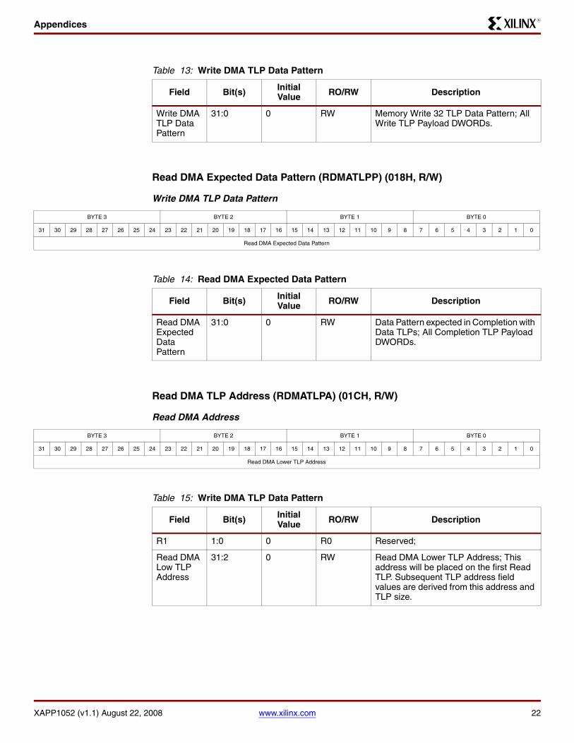
Read DMA Expected Data Pattern (RDMATLPP) (018H, R/W)
Write DMA TLP Data Pattern
Read DMA TLP Address (RDMATLPA) (01CH, R/W)
Read DMA Address
Table 13: Write DMA TLP Data Pattern
Field Bit(s) Initial Value RO/RW Description
Write DMA TLP Data Pattern
31:0 0 RW Memory Write 32 TLP Data Pattern; All Write TLP Payload DWORDs.
BYTE 3 BYTE 2 BYTE 1 BYTE 0
31 30 29 28 27 26 25 24 23 22 21 20 19 18 17 16 15 14 13 12 11 10 9 8 7 6 5 4 3 2 1 0
Read DMA Expected Data Pattern
Table 14: Read DMA Expected Data Pattern
Field Bit(s) Initial Value RO/RW Description
Read DMA Expected Data Pattern
31:0 0 RW Data Pattern expected in Completion with Data TLPs; All Completion TLP Payload DWORDs.
BYTE 3 BYTE 2 BYTE 1 BYTE 0
31 30 29 28 27 26 25 24 23 22 21 20 19 18 17 16 15 14 13 12 11 10 9 8 7 6 5 4 3 2 1 0
Read DMA Lower TLP Address
Table 15: Write DMA TLP Data Pattern
Field Bit(s) Initial Value RO/RW Description
R1 1:0 0 R0 Reserved;
Read DMA Low TLP Address
31:2 0 RW Read DMA Lower TLP Address; This address will be placed on the first Read TLP. Subsequent TLP address field values are derived from this address and TLP size.
Appendices
XAPP1052 (v1.1) August 22, 2008 www.xilinx.com 23
R
Read DMA TLP Size (RDMATLPS) (020H, R/W)
Read DMA TLP Size
Read DMA TLP Count (RDMATLPC) (024H, R/W)
Read DMA TLP Size
Write DMA Performance (WDMAPERF) (028H, R0)
Write DMA Performance
BYTE 3 BYTE 2 BYTE 1 BYTE 0
31 30 29 28 27 26 25 24 23 22 21 20 19 18 17 16 15 14 13 12 11 10 9 8 7 6 5 4 3 2 1 0
Read DMA Upper LTLP Address R1 TC R0 Read DMA TLP Size
Table 16: Read DMA TLP Size
Field Bit(s) Initial Value RO/RW Description
Read DMA TLP Size
12:0 0 RW Memory Read TLP Read Length in DWORDs (1 DWORD = 4 Bytes); 01H<=Length<=1FFFH;
R0 15:13 0 R0 Reserved
Read DMA TLP TC
18:16 0 RW Memory Read TLP Traffic Class; Controls Traffic Class field of the generated TLP.
64bit Read TLP Enable
19:19 0 RW 64bit Write TLP Enable; Setting this bit enables 64b Memory Read TLP generation.
R1 23:20 0 R0 Reserved
Read DMA Upper TLP Address
31:24 0 RW Read DMA Upper TLP Address; 64b Transaction Address bits[39:32]. Bits [63:40] will always be 0.
BYTE 3 BYTE 2 BYTE 1 BYTE 0
31 30 29 28 27 26 25 24 23 22 21 20 19 18 17 16 15 14 13 12 11 10 9 8 7 6 5 4 3 2 1 0
Memory Read 32 TLP Count
Table 17: Read DMA TLP Count
Field Bit(s) Initial Value RO/RW Description
Read DMA TLP Count
15:0 0 RW Memory Read 32 TLP Count;01D<=Count<=65535D
Reserved 31:16 0 R0 Reserved
BYTE 3 BYTE 2 BYTE 1 BYTE 0
31 30 29 28 27 26 25 24 23 22 21 20 19 18 17 16 15 14 13 12 11 10 9 8 7 6 5 4 3 2 1 0
Number of Interface Clock Cycles for Write
Appendices
XAPP1052 (v1.1) August 22, 2008 www.xilinx.com 24
R
Table 18: Write DMA Performance
Field Bit(s) Initial Value RO/RW Description
Write DMA Perfor-mance Counter
31:0 0 R0 Number of Interface Clock Cycles for Write DMA transfer to complete; Cycle time depends on Core Interface Data Path (DCSR) value.• x8 = 4 ns cycle time• x4 = 8 ns cycle time for 64 bit, 4 ns
cycle time for 32 bit• x1 = 32 ns cycle time for 64 bit, 16 ns
cycle time or 32 bitCleared by Initiator Reset;
Appendices
XAPP1052 (v1.1) August 22, 2008 www.xilinx.com 25
R
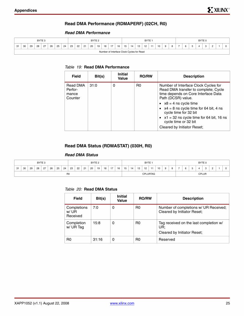
Read DMA Performance (RDMAPERF) (02CH, R0)
Read DMA Performance
Read DMA Status (RDMASTAT) (030H, R0)
Read DMA Status
BYTE 3 BYTE 2 BYTE 1 BYTE 0
31 30 29 28 27 26 25 24 23 22 21 20 19 18 17 16 15 14 13 12 11 10 9 8 7 6 5 4 3 2 1 0
Number of Interface Clock Cycles for Read
Table 19: Read DMA Performance
Field Bit(s) Initial Value RO/RW Description
Read DMA Perfor-mance Counter
31:0 0 R0 Number of Interface Clock Cycles for Read DMA transfer to complete; Cycle time depends on Core Interface Data Path (DCSR) value.• x8 = 4 ns cycle time• x4 = 8 ns cycle time for 64 bit, 4 ns
cycle time for 32 bit• x1 = 32 ns cycle time for 64 bit, 16 ns
cycle time or 32 bitCleared by Initiator Reset;
BYTE 3 BYTE 2 BYTE 1 BYTE 0
31 30 29 28 27 26 25 24 23 22 21 20 19 18 17 16 15 14 13 12 11 10 9 8 7 6 5 4 3 2 1 0
R0 CPLURTAG CPLUR
Table 20: Read DMA Status
Field Bit(s) Initial Value RO/RW Description
Completions w/ UR Received
7:0 0 R0 Number of completions w/ UR Received; Cleared by Initiator Reset;
Completion w/ UR Tag
15:8 0 R0 Tag received on the last completion w/ UR;Cleared by Initiator Reset;
R0 31:16 0 R0 Reserved
Appendices
XAPP1052 (v1.1) August 22, 2008 www.xilinx.com 26
R
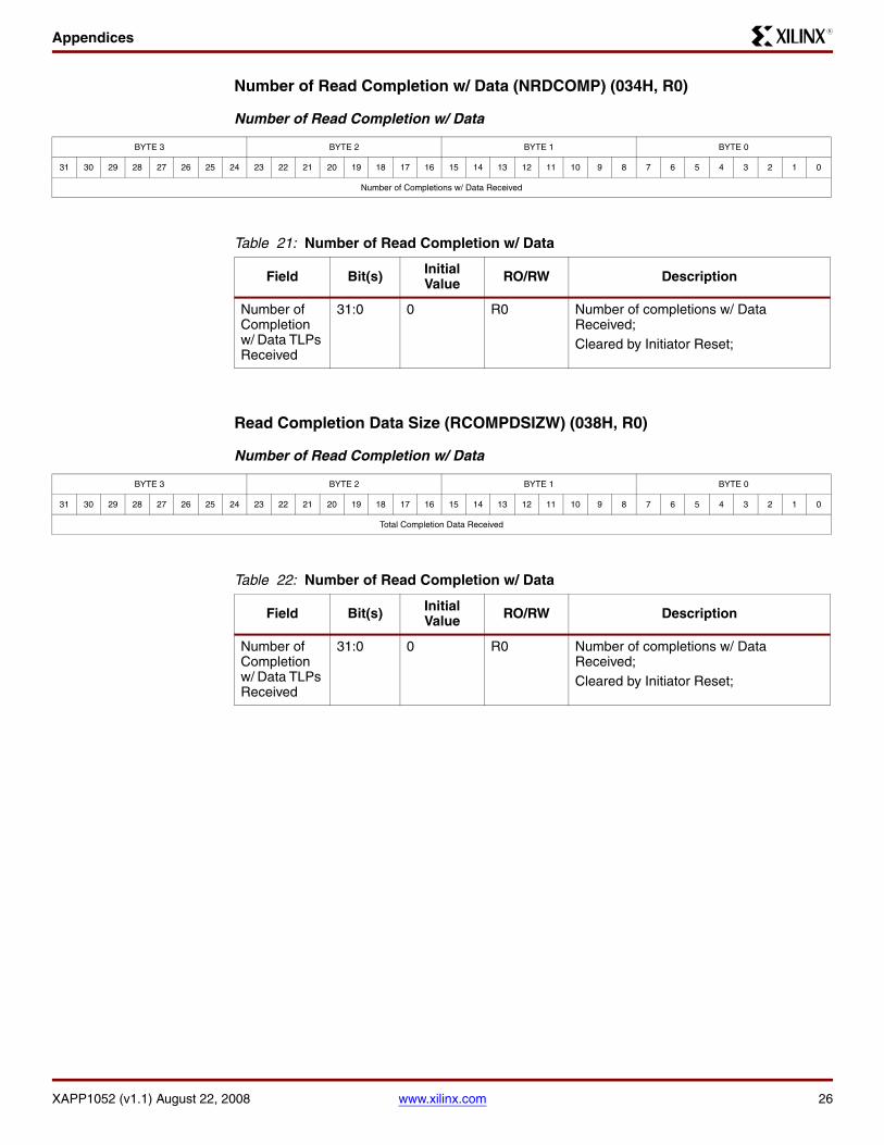
Number of Read Completion w/ Data (NRDCOMP) (034H, R0)
Number of Read Completion w/ Data
Read Completion Data Size (RCOMPDSIZW) (038H, R0)
Number of Read Completion w/ Data
BYTE 3 BYTE 2 BYTE 1 BYTE 0
31 30 29 28 27 26 25 24 23 22 21 20 19 18 17 16 15 14 13 12 11 10 9 8 7 6 5 4 3 2 1 0
Number of Completions w/ Data Received
Table 21: Number of Read Completion w/ Data
Field Bit(s) Initial Value RO/RW Description
Number of Completion w/ Data TLPs Received
31:0 0 R0 Number of completions w/ Data Received;Cleared by Initiator Reset;
BYTE 3 BYTE 2 BYTE 1 BYTE 0
31 30 29 28 27 26 25 24 23 22 21 20 19 18 17 16 15 14 13 12 11 10 9 8 7 6 5 4 3 2 1 0
Total Completion Data Received
Table 22: Number of Read Completion w/ Data
Field Bit(s) Initial Value RO/RW Description
Number of Completion w/ Data TLPs Received
31:0 0 R0 Number of completions w/ Data Received;Cleared by Initiator Reset;
Appendices
XAPP1052 (v1.1) August 22, 2008 www.xilinx.com 27
R
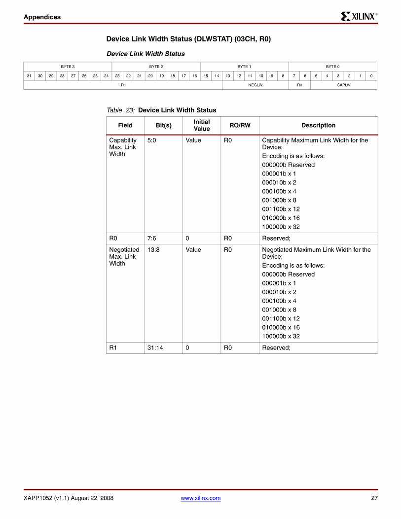
Device Link Width Status (DLWSTAT) (03CH, R0)
Device Link Width Status
BYTE 3 BYTE 2 BYTE 1 BYTE 0
31 30 29 28 27 26 25 24 23 22 21 20 19 18 17 16 15 14 13 12 11 10 9 8 7 6 5 4 3 2 1 0
R1 NEGLW R0 CAPLW
Table 23: Device Link Width Status
Field Bit(s) Initial Value RO/RW Description
Capability Max. Link Width
5:0 Value R0 Capability Maximum Link Width for the Device;Encoding is as follows:000000b Reserved000001b x 1000010b x 2000100b x 4001000b x 8001100b x 12010000b x 16100000b x 32
R0 7:6 0 R0 Reserved;
Negotiated Max. Link Width
13:8 Value R0 Negotiated Maximum Link Width for the Device;Encoding is as follows:000000b Reserved000001b x 1000010b x 2000100b x 4001000b x 8001100b x 12010000b x 16100000b x 32
R1 31:14 0 R0 Reserved;
Appendices
XAPP1052 (v1.1) August 22, 2008 www.xilinx.com 28
R
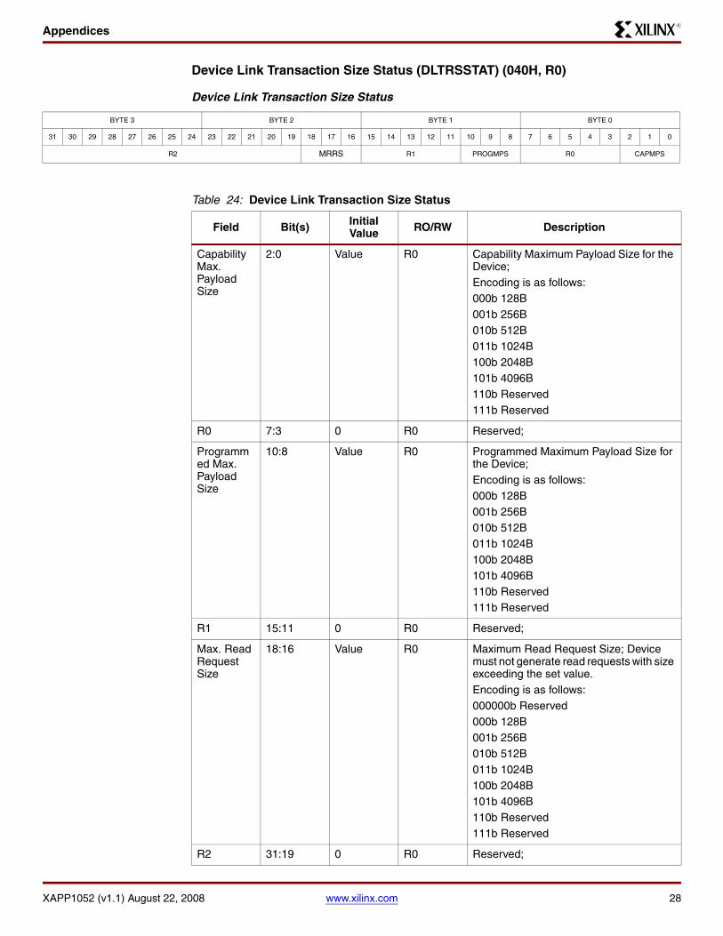
Device Link Transaction Size Status (DLTRSSTAT) (040H, R0)
Device Link Transaction Size Status
BYTE 3 BYTE 2 BYTE 1 BYTE 0
31 30 29 28 27 26 25 24 23 22 21 20 19 18 17 16 15 14 13 12 11 10 9 8 7 6 5 4 3 2 1 0
R2 MRRS R1 PROGMPS R0 CAPMPS
Table 24: Device Link Transaction Size Status
Field Bit(s) Initial Value RO/RW Description
Capability Max. Payload Size
2:0 Value R0 Capability Maximum Payload Size for the Device;Encoding is as follows:000b 128B001b 256B010b 512B011b 1024B100b 2048B101b 4096B110b Reserved111b Reserved
R0 7:3 0 R0 Reserved;
Programmed Max. Payload Size
10:8 Value R0 Programmed Maximum Payload Size for the Device;Encoding is as follows:000b 128B001b 256B010b 512B011b 1024B100b 2048B101b 4096B110b Reserved111b Reserved
R1 15:11 0 R0 Reserved;
Max. Read Request Size
18:16 Value R0 Maximum Read Request Size; Device must not generate read requests with size exceeding the set value.Encoding is as follows:000000b Reserved000b 128B001b 256B010b 512B011b 1024B100b 2048B101b 4096B110b Reserved111b Reserved
R2 31:19 0 R0 Reserved;
Revision History
XAPP1052 (v1.1) August 22, 2008 www.xilinx.com 29
R
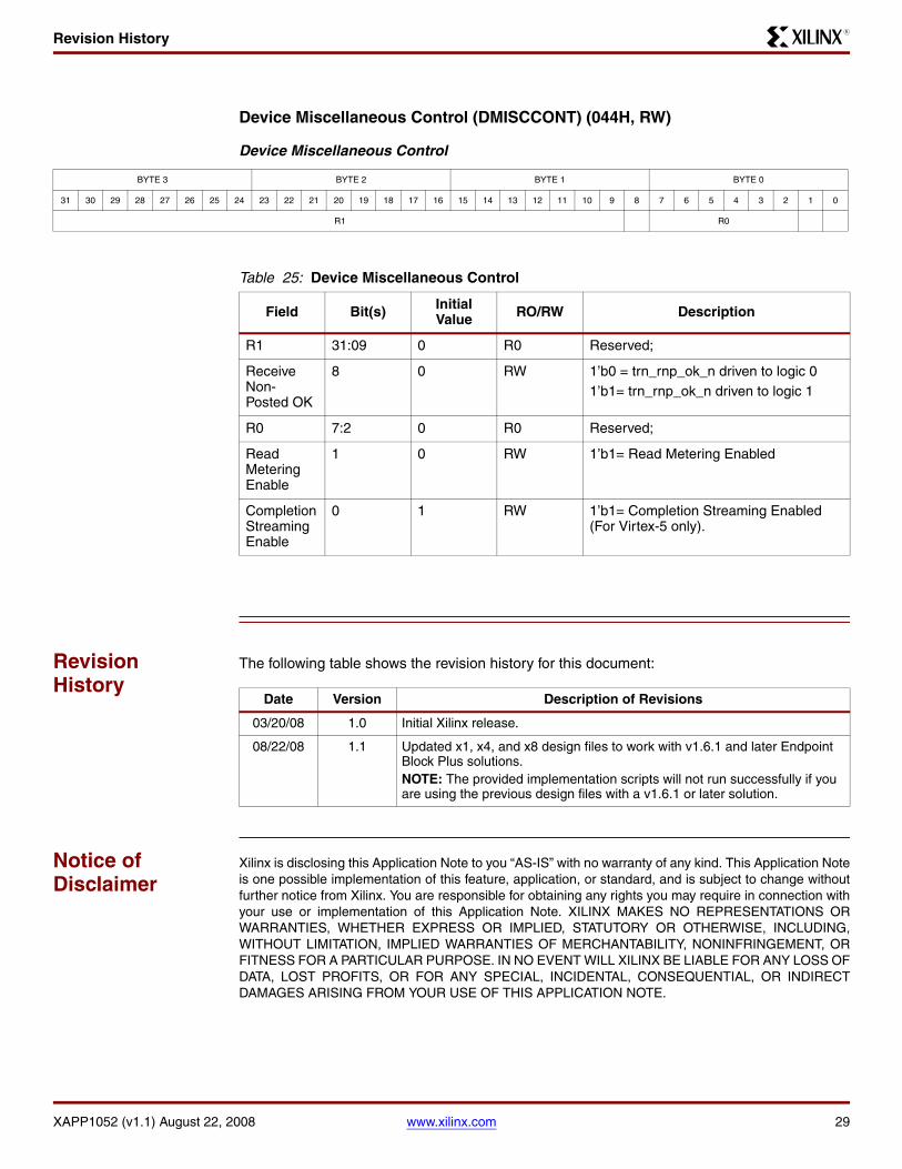
Device Miscellaneous Control (DMISCCONT) (044H, RW)
Device Miscellaneous Control
Revision History
The following table shows the revision history for this document:
Notice of Disclaimer
Xilinx is disclosing this Application Note to you “AS-IS” with no warranty of any kind. This Application Noteis one possible implementation of this feature, application, or standard, and is subject to change withoutfurther notice from Xilinx. You are responsible for obtaining any rights you may require in connection withyour use or implementation of this Application Note. XILINX MAKES NO REPRESENTATIONS ORWARRANTIES, WHETHER EXPRESS OR IMPLIED, STATUTORY OR OTHERWISE, INCLUDING,WITHOUT LIMITATION, IMPLIED WARRANTIES OF MERCHANTABILITY, NONINFRINGEMENT, ORFITNESS FOR A PARTICULAR PURPOSE. IN NO EVENT WILL XILINX BE LIABLE FOR ANY LOSS OFDATA, LOST PROFITS, OR FOR ANY SPECIAL, INCIDENTAL, CONSEQUENTIAL, OR INDIRECTDAMAGES ARISING FROM YOUR USE OF THIS APPLICATION NOTE.
BYTE 3 BYTE 2 BYTE 1 BYTE 0
31 30 29 28 27 26 25 24 23 22 21 20 19 18 17 16 15 14 13 12 11 10 9 8 7 6 5 4 3 2 1 0
R1 R0
Table 25: Device Miscellaneous Control
Field Bit(s) Initial Value RO/RW Description
R1 31:09 0 R0 Reserved;
Receive Non-Posted OK
8 0 RW 1’b0 = trn_rnp_ok_n driven to logic 01’b1= trn_rnp_ok_n driven to logic 1
R0 7:2 0 R0 Reserved;
Read Metering Enable
1 0 RW 1’b1= Read Metering Enabled
Completion Streaming Enable
0 1 RW 1’b1= Completion Streaming Enabled (For Virtex-5 only).
Date Version Description of Revisions
03/20/08 1.0 Initial Xilinx release.
08/22/08 1.1 Updated x1, x4, and x8 design files to work with v1.6.1 and later Endpoint Block Plus solutions.NOTE: The provided implementation scripts will not run successfully if you are using the previous design files with a v1.6.1 or later solution.