applications of chfl,•jh.: th.ansfef:l devices … workshops/dick bredthauer...
TRANSCRIPT

APPLICATIONS OF CHfl,•JH.: Th.ANSFE"f:l DEVICES IN TELEVISION
B.H.J. Cornelissen,*L.J.M. Esser*and L.J. van de Polder*
1 . INTRODUCTION
A charge transfer device (CTD) is a solid state device 1n which analogue signal samples can be - stored
Proper combinations of these application areas
- transferred - inserted, electrically or optically - detected, destructively and non-destruc-
tively. basic functions lead to the following main
- time axis conversion - filtering - imaging
This was recognized already with the introduction of the CTD by Sangster and Teer ( 1 ) .
The quality of present types of CTD permit their application in TV systems. Due to the combination of simple structure and excellent basic properties they potentially offer a drastic simplification of several contemporary circuits and allow the introduction of new functions in professional and consumer products. Experimental results justify the expectation that in video signal processing the first applications will mainly be in the area of time axis conversion and filtering,viz. time error correction, TV standards conversion and ghost suppression.
2. TV AND CTD
In the following the application of CTDs in TV systems will be discussed. Therefore, in this section first some fundamental aspects of TV systems will be recapitulated. If no special system is mentioned, the PAL system will be assUIIled.
2. 1 ~~~~=~!: In a camera the picture is scanned line by line in the so-called interlaced scanning mode. If a CTD-sensor is applied, this interlaced scann1ng is effectively accomplished. With conventional pick-up tubes the amplitude of the output signal is a linear or non-linear function of the light input depending on the photosensitive layer that is used. With CTDs a linear relationship normally exists between signal output and light input (fig. 1a). It is normal practice to correct at the pick-up side for the non-linear relation between the drive voltage and the light-output of the cathode r~ tube used at the receiving side; this correction at the pick-up side is called "gamma correction" (fig. 1b). The effect of this gamma correction is that the gain at a low brightness level is much higher than at a high brightness level. Considering the signal-to-noise ratio it is worthwhile to take this gamma correction into account. For weighting the signal-to-
*Fhilips Research Laboratories, Eindhoven, The Netherlands
348

noise ratio of a gamma corrected video signal the following formula (2) may be used
( 2. 1 )
where N , N and ~ are the effective values of the noise superimposed at respect!vel~ white, gray and nearly black signal levels. This shows that noise added to the video signal before the gamma correction is much more harmful if it is added at a low brightness level than if it is added at a high brightness level. This situation is also to be expected if CTDs are used as pick-up devices.
2.2 Transmission
With colour television a coding method is applied for the transmission of the two colour information, whereas the luminance information (the blackand-white signal) is transmitted in a conventional way. The bandwidth of the luminance signal is 5 MHz, the bandwidth of the two colour information · is about 1 MHz. These latter two informations are modulated on a carrier which is added to the luminance signal. In the NTSC and the PAL systems, amplitude and phase modulation are applied for the colour coding (Fig. 2). Because of non-linear effects it may happen that the amplitude or the phase is distorted as a function of the level of the luminance signal : the so-called differential gain and differential phase errors. Normally it is required that in a complete system the total differential gain error should be less than about ten percent, and the total differential phase error should be smaller than say 20°. This means that if a CTD is used for a specialxequiremen~the errors introduced by the CTD should only be a fraction of the above quoted values.
2.3 ~~~~~~~~ In the case of the NTSC and the PAL systems the decoding of the two colour difference signals in the receiver is carried out via synchronous demodulation. With this type of demodulation one needs a reference carrier. In the receiver this carrier is regenerated using a burst which is transmitted during the line blanking interval (Fig. 3). In order to be able to regenerate the carrier with sufficient phase acc~acy, the carrier frequency should be very accurate (tolerance < 3. 10- ) •
2.4 ~~!E!~l For the reconstruction of the picture at the receiving side the scanning beam should be synchronized with that at the pick-up side. Therefore horizontal and vertical synchronizing signals are transmitted. If no visible position errors are allowed, the disturbance in position between succeeding scanning lines should be smaller than the size of one picture element. This corresponds to a timing error smaller than 100 ns.
3. PROPERTIES OF CTDs
3.1 Charge storage . --------------A CTD is inherently a dynamic memory. This is caused by the thermally generated dark current which will fill the potential wells and swamp the charge packets which are stored in the CTD. At room temperature the magnitude of the charge produced by the dark current during one field
349

period (20 ms) cannot be ignored. For a continuously clocked device, or if this dark current is uniformly distributed over the device, the dark current will only limit the magnitude of the signal charge packets that can be handled and will deteriorate the signal-to-noise ratio. If the dark current is not uniformly distributed it may give rise to a fixed pattern noise depending on its operation mode. Subjectively this may be very disturbing. The random fluctuation of the dark current has a shot noise character (3).
3.2 ~~~~~~-~~~~!~~ In the CTD there are several mechanisms which give rise to an incomplete transfer. The fractional charge which remains after one transfer is called the transfer inefficiency £ . This transfer inefficiency is almost constant up to the maximum clock rate of the device. Above this clock rate, € increases strongly with the clock frequency. In practice, for E , values of 1o-3 to 1o-5 are found. As it is a cumulative effect, the overall inefficiency depends on the total number of transfers. The transfer inefficiency product is equal to Np€ , where N is the number of stages and p is the number of gates per stage. One stage contains one charge packet. The transfer inefficiency influences the frequency characteristic. The frequency dependent amplitude attenuation (fig. 4) is given by (4)
f exp [ -Npe (1-cos 211' fc)] ( 3. 1 )
where fc 1s the clock frequency and also the sampling rate of the input signal. By means of a correction amplifier we can correct for the frequency response given by eq. (3.1). The additional phase shift with respect to the ideal case (€ =0) is given by
1::. ~ = Npe sin 211' :c (3.2)
and the additional group delay (fig. 5)
t:.r = dt:.cp = Npe cos 211'f dw fc fc
(3.3)
For a practical case of N = 1000, p = 4, € = 5 x 10⁻⁵ , 0 < f < fc/2, fc = 12.5 MHz is found
and
O.l < Aout < 1 A in
-16ns < 1::. r < 16ns
These values are quite permissible in TV.
350
(3.4)
(3.5)
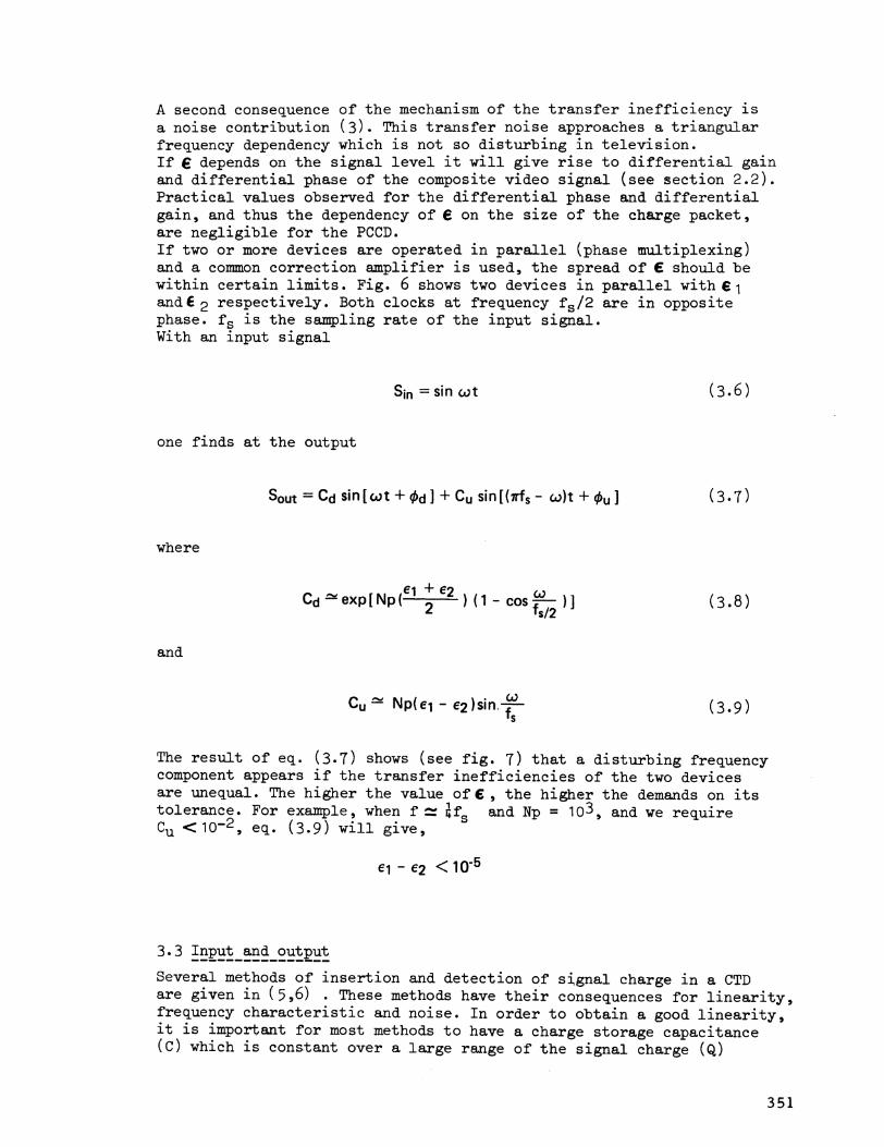
A second consequence of the mechanism of the transfer inefficiency is a noise contribution (3). This transfer noise approaches a triangular frequency dependency which is not so disturbing in television. If € depends on the signal level it will give rise to differential gain and differential phase of the composite video signal (see section 2.2). Practical values observed for the differential phase and differential gain, and thus the dependency of e on the size of the charge packet, are negligible for the PCCD. If two or more devices are operated in parallel (phase multiplexing) and a common correction amplifier is used, the spread of € should be within certain limits. Fig. 6 shows two devices in parallel withE1 andE 2 respectively. Both clocks at frequency fs/2 are in opposite phase. fs is the sampling rate of the input signal. With an input signal
Sin= sin wt (3.6)
one finds at the output
Sout = Cd sin[wt + 4>d] + Cu sin[(1lf5 - w)t + 4>u] (3.7)
where
e1 + e2 w Cd !::>< exp [ Np ( 2 ) ( 1 - cos -f - ) ]
s/2 (3 .8)
and
(3.9)
The result of eq. (3.7) shows (see fig. 7) that a disturbing frequency component appears if the transfer inefficiencies of the two devices are unequal. The higher the value of € , the higher the demands on its tolerance. For example, when f ~ afs and Np = 103, and we require Cu <:1o-2 , eq. (3.9) will give,
3.3 !~R~~-~~-~~~R~~ Several methods of insertion and detection of s~gnal charge in a CTD are given in (5,6) . These methods have their consequences for linearity, frequency characteristic and noise. In order to obtain a good linearity, it is important for most methods to have a charge storage capacitance (C) which is cons.tant over a large range of the signal charge (Q)
351

Q = C Vsignal (3.10)
For a luminance signal the demands on linearity of the transformation are not so severe, provided that the video signal is clamped (d.c. coupled). The ampiitude vs frequency characteristic of the input and output method depends on the effective sampling time and hold time (1r), respectively. It is given by the Fourier transform of the sampling and hold function
G(f) =sine (fed (3.11)
where fc is the clock frequency.
Sampling of a charge quantity at the charge storage capacitance (C) at the input or resetting the output capacitance (C) prior to the detection of the delayed charge quantity introduces in both cases a thermal noise (7) expressed by
Onoise = (kTC) 112 (3.12)
where k denotes Boltzmann's constant and T temperature K. The contribution of this type of noise is independent of the signal level and rather low.
3.4 ~~~~-!~E~-~!_2~~-!~E-~~~~~-~~~~~~-EE~S~~~!~~? As will be shown in the next section in some application~ one needs for video processing,clock frequencies of at least up to 30 MHz. This requirement can be fulfilled with bipolar bucket brigade devices, buried channel CCDs and PCCDs. Only bulk CCDs can be used if low transfer inefficiencies of say 1o-4 to 10-5 are required. The additional combination of high speed transfer (up to 180 MHz) and high charge handling capacity (high S/N) is found for the twin layer PCCD (6,9 ).
4. TV APPLICATIONS OF CTDs
4.1 Time conversion
When the transfer-rate or clock frequency is constant. the CTD will show a fixed delay. If the cJock frequency is changed relatively slowly, so that ~h0 clock frequency does not change considerably during the delay time of the device, the CTD gives a continuously variable delay time. Another possibility is to load the CTD register with one television !ine at a constant clock frequency, as soon as the CTD is fi:J..led th·-· clock is stopped for a certain time and after that the original clock frequency is switched on again in order to shift out the information. In this way a switched delay is obtained. When the CTD is loadedwith one clock frequency and unloaded with another frequency, a time compression or expansion is obtained. If we load a CTD and switch the transfer direction we will get time inversion. All these examples of time conversion will be described in more detail in the next sections. 352

4.1.1 ~~-~!~-~~~~-~~-~-!~~~~-~~~~~-!~~~ When charge packets are transferred they will induce displacement currents in the clock line, and as the clock driver has a non-zero internal impedance the clock amplitude will be influenced by the sum of the charge packets in the d~vice. In CTDs operated in the complete transfer mode,this variation in clock amplitude will not influence the transfer process itself. However problems may occur in the sampling stage at the input, for, the magnitude of the charge packet that is formed is not only a function of the video input signal, but also of the clock amplitude, and so the sampling stage needs a separate clock driver. At a clock frequency of 13 MHz or higher the cross-talk from the clock to the input electrode cannot be ignored. (This signal is synchronously detected by the sampling mechanism and will give rise to a d.c. level shift of the signal charge). Also, the cross-talk from input to output and vice versa may be important . In general this type of cross-talk gives a ghost in the reproduced picture. Therefore the design and layout of the CTD and its associated circuits should be such that this crosstalk is as low as possible. The information arrives at the output at regular intervals T in the form of charge samples as given in fig. 8a. The corresponding frequency spectrum is given in fig. 8b. The information carried by the charge packets is present in the zero order spectrum but it is also present ln the first and higher order spectra. If the amplifier is followed by a lowpass filter we will find the zero order spectrum. Sometimes it will be advantageous to use the first order spectrum. A method to detect this first order spectrum is known as correlated double sampling (3 ). As demonstrated below the same result will be obtained with synchronous detection, in which case the reference signal has to be the clock signal. The noise spectrum determines whether the zero order or the first order spectrum will give better results. In case of a built-in output amplifier the l.f. flicker noise will dominate the noise spectrum (10 ). In this case the first order spectrum will have a better S/N ratio than the zero order spectrum. In case of an external output amplifier the noise contribution is mainly determined by h.f. noise. In that case the zero order spectrum is to be preferred. We will now show that synchronous detection is equivalent to the correlated double sampling. In the correlated double sampling method the signal is sampled (measured) twice every period. First, the background charge is measured, next the background and the signal charge are measured together. These two values are subtracted in order to eliminate the low frequency noisy background signal. The second description is that the CTD output signal (fig. 9a) is multiplied by the sampling function of fig. 9b. This multiplication with the function of fig. 9b is known as balanced synchronous detection. The sampling time can vary between almost zero and 1/2fc.
The sampling waveform for that case is given in fig. 9c, and a simplified diagram of such a circuit with the integrated circuit TCA 240 is given ln fig. 10. Strictly speaking the input of the synchronous demodulator should be bandpass limited· Frequencies in the neighbourhood of 3 fc, 5 fc, and so on, should be suppressed.
353

A fixed delay line with a delay of 64f's and a bandwidth of 5 MHz can be used in a TV camera for vertical aperture correction. In professional video recorders, it can be used for drop out correction and also for "prediction" of time errors.
4.1.2 ~~~!~~~~~~~~-~~~~~~~~-~~~~~ A CTD can be used as a variable delay line by changing the clock fre-quency. If this frequency is changed between f . and f we will get a change in delay of mln max
N f . L:.rm = -- ( 1 -~ )
fmin fmax (4.2)
If a composite signal is to be handled, the m1n1mum clock frequency will be 13.3 MHz. With a maximum clock frequency of 26.6 MHz the delay variation will be Nx37 ns. With a maximum clock frequency of 40 MHz this delay variation will be Nx50 ns (fig. 11). Consequently, for this application, the CTD must be able to operate at a clock frequency in the range of 30 to 40 MHz. Clock driver circuits which are used are given in fig. 12a, b or c. With the circuit of fig. 12a, fmax of 40 MHz, a capacitance of 20 pF and a peak to peak clock signal of 10 V the power dissipation per clock driver will be
(4.3)
The clock drivers have to be wired carefully in order to prevent r.f. radiation. As the transfer inefficiency product influences the frequency characteristic (eq. (3.1)), the frequency characteristic will also be a function of the clock frequency. A variable delay line can be used for correcting time errors of the video signal from a video tape recorder or from a video long-play recorder. With a CTD with 256 stages a time error 1n the range of 10JUS can be corrected. A variable delay line may also be used for the correction of the horizontal superposition errors in a TV colour camera or of the horizontal convergence errors of a TV colour receiver.
4.1.3 ~~~!~~~~-~~~~~ Another method to obtain a variable delay is to store a video signal for a variable time. An implementation may be as follows: The frequency of a master clock is divided by 4 (fig. 13). This dividerby-4 delivers the four phases for the CTD and is also a digital memory for the case that the master-clock is switched off, when thQ·waiting time starts. For a complete set-up we need three devices: the first is read in, the second is waiting and the third is read out. These functions are c;/clically changed. The minimum step in the delay variatic:m is 1/4fc which is about 19 nanoseconds, for a clock frequency of 13.3 MHz. In a practical set up the time fault will be corrected in two steps. The first step brings back the time fault from 10 p s to within 100 ns, the reference in this case being the horizontal synchronization signal. The second step reduces the time fault to within 5 ns, the reference in this case is the colour burst signal. 354

If the CTDs have such a length that they are able to store one television line, we do not need to switch during the active line, because this will be difficult. The three devices should have small tolerances on inefficiency e , on the dark current and on the linearity (section 3).
4.1.4 !!~~-~~~£~~~~!~~-~~~-~~~~!~~ A video signal can be compressed or expanded 1n time with the aid of a charge transfer device. The method is as follows: the video signal is sampled and shifted into a CTD with a clock frequency f1 until the CTD is filled. After some waiting time ·the information 1s shifted out of the CTD, using a clock frequency f2. The compression (or expansion )factor is then equal to f1/f2. This capability may be employed for TV standards conversion. If TV standards are different two possibilities have to be distinguished, either the picture frequencies are different, or the picture frequencies are equal but the numbernof lines per picture are different. An example of the first possibility is the 60 Hz TV standard as employed in the U.S.A. and the 50 Hz TV standard as employed in Europe. It can be shown that for the conversion between these TV standard~ field stores are required (11 ). Such field stores must have a capacity of about two hundred thousand analogue samples each. Because of the large storage time required, it is to be expected that in future the digital signal treatment is the best solution for this type of TV standards conversion. If however the picture frequencies of the two standards are equal and only the numbers of lines per picture are different, then the analogue conversion using CTDs, looks very promising. As an example, our laboratory is investigating using PCCDs, the conversion from the normal TV broadcast standard with 625 lines into the videophone standard with 313 lines, and vice versa; both standards having 25 pictures per second (12,13). In this way we are able to distribute and display the standard broadcast signal via the videophone network and also to display the videophone signal on a standard monitor. A similar conversion is required for the conversion from the 625-line system into a high resolution TV system with about 1250 lines. The block diagram of the circuit for the conversion from 625 into 313 lines is shown in fig. 14. The principle of the conversion system is that during a picture period every second video line of the original 625-line signal is used for the conversion. These lines are alternately fed into the two shift registers D1 and D2 by means of the electronic switch S. This is shown in more detail in fig. 15. The advantage of the 313-line system is that this conversion can be carried out using only two shift registers. If a clock frequency of 5 MHz is used for reading in then the number of samples per shift register (CTD) is 320. With this application special demands for the CTDs are, 1st The input-output characteristics of the two CTDs in the two chan
nels must be equal (if not, a disturbing half line crawl appears in the converted picture);
2nd The dark current of all elements in a CTD must be small or equal. Since, the information is waiting in the CTD for some time, a large dark current of only one of the elements of the CTD will result in a disturbing vertical line in the converted picture.
Another application of the method of time compression and expansion 1s in the field of TV recording. In normal TV recording crosstalk may occur between the luminance, the colour difference and the sound signals.
355

A possibility to remove this crosstalk is to use only one signal channel and to separate the signals in time. The signals are shifted and compressed to get the following time sharing model: during the 64 p s of one television line we use 40 p. s for the luminance signal (compression ratio 1,3), 8p.s for (R-Y) (compression ratio 6,5), Bps for (B .... Y) (compression ratio 6,5) and 4JUs for sound (compression ratio 16) and the remaining 4fls for synchronization.
4.1.5 Time inversion
When a CTD is loaded with a signal and the transfer direction is reversed, the stored signal will be reversed in time. In this way the CTD functions as an electronic mirror. This mirror function can be used for electron-ic tricks. For this operation the signal has to be chopped into pieces
of time which can be stored in the CTD. A television signal is very well suited, because it is already divided in television lines. Another application is in the field of filters. With the aid of a time inverter we are able to obtain a constant group delay. It works as follows. When a video signal is filtered in a lowpass filter and shifted into a CTD we see that after reversing the transfer direction, the part of the frequency spectrum that encountered a larger group delay in the filter will appear before the part of the frequency spectrum that encountered a smaller group delay, the time axis being inverted. If now the reversed signal passes a filter identical with the first filter, the sum of both group delay characteristics will be constant (14).
4.2 ~~~~~!~~~
4.2.1 !Y .... Q~~~!_§~EE!~~~~~~ The signal that is received at the TV antenna may consist of the sum of the desired direct signal and one or more undesired reflected signals which are attenuated and delayed with respect to the desired signal. The detected video signal will be disturbed by the reflections. The amplitude of this reflected signal is determined by the strength of the reflection and by the phase relationship between the carrier of the direct signal and the carrier of the reflected signal. The phase relation ~ that the detected reflection shows a positive or a negative polarity. If the amplitude ratio of the detected echo and of the main signal is more than 1% and the delay time 1"' is more than say 1 1-' s, then the displayed picture is visually disturbed (16). Therefore elimination of the ghost is desirable. It is possible to apply a CTD for this correction. The task is to delay the detected video signal over a time tr and to add (or subtract) a fraction ~of this delayed signal to the main signal. The time '('"can be adjusted by choosing the proper clock frequency for the CTD or by adjusting the corresponding tap weight to - ~ of a CTD transversal filter with variable tap weights. The main signal and the reflected signal at 'f' sec are delayed 't"' sec. This means that after the multiplication (~) and addition the original echo at'\ is eliminated but a new reflection with amplitude ct2 at 2'\sec is created. In the case of the transversal filter this second order delayed signal can be eliminated by adjustment of the corresponding tap weight at 2 'l to 0(.2, and so on (fig. 16). If 1~1 is smaller than 22% it is sufficient to compensate up to the third order echo <I« 13 < 0. 01 ) . An echo with a very short delay, in the order of 0.1ps, is subjectively less annoying So for normal reception this 356

type needs no elimination. By means of a recursive filter (fig. 17) one needs per echo only one tap at the correct delay. In that case no higher order reflections occur. Such a ghost suppression circuit for one echo is treated in (16,1(). Also in (16) methods enabling an automatic ~8$urement of the polarity and the value of ~ are discussed. Misadjustments in a and or ~ introduce a decreasing series of ghosts at 't' , 2't'", 3'r, etc., for this circuit.
4.2.2 £~~~-!!!~~~!~~ In the PAL television system the use of a delay line of 6~s gives the possibility to correct certain phase faults in the chrominance channel. The glass delay line in use nowadays has a center frequency of 4.43 MHz and a bandwidth of 2 MHz (fig. 18). It is possible to obtain the same results with two delay lines, each with a passband from 0 to 1 MHz, one for each colour difference signal (fig. 19). With CTDs a delay line for the chrominance signal needs 851 stages and a clock frequency of 13.3 MHz; the delay lines for the colour difference signals need about 140 stages and a clock frequency of 2.2 MHz. The glass delay line which is used in a receiver is very cheap and it does not need a clock signal, so, it is improbable that it will soon be replaced by a CTD. In the NTSC system, the application of a dela;y line of 63.5jls and with a passband from 0 to 4 .. 5 MHz gives the possibility to separate the chrominance and the luminance signals .• This method might be employed in new high quality NTSC colour receivers and it can be very useful in a standards-convertor where the input signal is the NTSC signal (fig.20). In the PAL system two delay lines of 64 p. s are needed to perform this chrominance-luminance separation. If a CTD is used for these delay lines, a good choice for the clock frequency will be three times the colour subcarrier frequency, in order to prevent interfering components. Comb filters are also frequently used in a number of systems for onetube colour cameras.
4.3 !~~!:;~ Solid state 1mage sensors can be subdivided into two groups: linear image sensors and area image sensors. In area image sensors the charge generated in the photodiodes is integrated during 20 or 40 ms but with a linear image sensor the integration time is only 64 p. s. In the latter case the illumination level has to be rather high. A possibility to use a linear sensor for film scanning is described in (15). The film is moved continuously, thus providing the vertical scanning. With this type of scanning no interlace is obtained, and so this set up as such delivers a non-standard video signal. By means of standards conversion a standard video signal can be made. Other applications of line sensors are in facsimile or in a slide scanner. The vertical scanning is again mechanical. If an area image sensor is used in a TV camera, the resolution will be determined by the number of elements. For standard TV we need in the vertical direction 600 elements and in the horizontal direction about 800 elements, the aspect ratio being 3 to 4. Attractive features of CTD image sensors are their immunity to shock, vibration and electromagnetic fields, their potential reliability, their long life, their infrared sensitivity and their geometrical properties. The last mentioned
357

property will give linear and stable scanning of the picture. Nowadays, problems of CTD image sensors are:the spread of the dark current, the spread of the sensitivity of the photo-diodes, the blooming which has a line geometry for area sensors, the low blue sensitivity and the low yield. Building a three-device colour camera with CTDs will give specific problems. With vidicons or Plumbicons it i~ possible to build cameras with a photo sensitive area of 6 x 8 mm • The colour splitting prismsand the lens have small dimensions. The sensitive area of a CTD with a comparable resolution will be larger, so the colour prism and the lens will be larger which outweighs the smaller and lighter image sensors. The zoom-lens of studio cameras in use nowadays does not give the same dimensions for the projected red, green and blue scenes. With an electronbeam scanned target it is quite easy to correct for these small differences, in dimensions. If a CTD is used in a colour TV camera it looks very difficult to change the scanned dimension electronically in the vertical direction or to obtain a geometrical shift. If only the visible part of the spectrum is taken into account, the sensitivity of a Si target and of an antimony trisulfide vidicon target do not differ so much. A CTD with line transfer has an effective light-sensitive area of 20 to 50 percent so the sensitivity is only 20 to 50 percent of a vidicon. With frame transfer combined with backside illumination, an effective area of 100 percent lS obtained.
5. CONCLUSION
In the foregoing it is shown that in principle several interesting applications of the CTD in television systems are possible. The prime applications of CTDs may be in the field of fixed and variable delay lines. Fixed delay lines may be used in comb filters and in filters for vertical aperture correction in TV cam~ras; variable delay lines may be used for echo cancellation and for time error correction in video recorders. In these applications large video signals can be handled, so the demands on the noise contribution of the CTD are low. In the case of fixed delay lines often a complete TV line has to be delayed. If a composite video signal is delayed a practical sample frequency will be 13.3 MHz; if in this case only one CTD is used the device should have a low transfer inefficiency (€ better than 5x1o-5). In the case of variable delay lines the clock frequency is changed from a low value (e.g. 13.3 MHz) to a higher frequency in the range of 30 to 40 MHz. Therefore the CTD must be able to operate at such high clock frequencies. With line and area image sensors on the other hand the demands on the noise contribution are much higher. This holds for the random noise added to the signal, but especially for the fixed pattern noise. The latter can be due to dark current spots of one or more of the elements or due to differences in sensitivity of the elements. Further, a large number of elements are required in the case of area sensors. Up till now the possibilities for the use of ima~e !~nsors look doubtful. Namely for professional use the image quality is too low, whereas for the consumer market the price probably will be too high. In this respect the appli~ation of line sensors looks more promising, possible fields being slide scanners and facsimile scanners.
358

REFERENCES
1. F.L.J. Sangster and K. Teer, "Bucket-brigade Electronics- new Possibilities for Delay, Time Axis Conversion and Scanning", IEEE J. Solid-State Circuits, vol. SC-4, pp. 131-136, June 1969.
2. R. Theile and H. Fix, "Zur Definition des durch die Sta.tistischen Schwankungen bestimmten Storabstandes im Fernsehen", Archiv. elektr. LJ'bertr., vol. 10, pp. 98-104, 1956.
3. R.W. Brodersen and S.P. Emmons, "Noise in buried channel ChargeCoupled Devices", IEEE Trans. Electron Devices, vol. ED-22, pp. 215-223, Feb. 1976.
4. W.B. Joyce and W.J. Bertram, "Linearized dispersion relation and Green's function for discrete-charge-transfer devices with incomplete transfer", Bell Syst. Tech. J., vol. 50, pp. 1741-1759, July-Aug. 1971.
5. C.H. Sequin and M.F. Tompsett, "Charge Transfer Devices", Advances in Electronics and Electron Physics, Suppl. 8, Academic Press, New York.
6. L.J .M. Esser, "Peristaltic Charge Coupled Devices : What is Special about the Peristaltic Mechanism", "Solid State Imaging", ed. P.G. Jespers, F. v.d. Wiele and M.H. White, Noordhoff Intl. Publishing, Leyden, The Netherlands, 1976, pp. 343-426.
7. J.E. Carnes and W.F. Kosonocky, "Noise Sources in Charge Coupled Devices", RCA Review, vol. 33, pp. 327-343, June 1972.
8. I. Takemote, S. Ohba, M. Kubo and M. Ashikawa, "A Wide-Band Low-Noise Charge Transfer Video Delay Line", IEEE J. Solid-State Circuits, vol. SC-9, pp. 415-422, Dec. 1974.
9. H.L. Peek, "Twin-layer PCCD Performance for Different Doping Levels of the Surface Layer, "IEEE J. Solid-State Circuits, vol. SC-11, pp. 167-170, Feb. 1976.
10. R.S. Cobbold, "Theory and Applications of Field Effect Transistors", Wiley & Sons, New York, 1970, p. 305.
11. J.L.E. Baldwin, A.D. Stalley, J.A. Coffey, R.L. Greenfield, I.R. Lever and J.H. Taylor, "DICE: the First International Digital Standard Converter", The Royal Tel. Soc . J. , vol. 16 , pp. 140-159, 1974.
12. M.C.W. van Buul and L.J. van de Polder, "Standards Conversion of a TV signal with 625 Lines into a Videophone signal with 313 Lines", Philips Res. Repts, vol. 28, pp. 377-390, 1973.
13. M.C.W. van Buul and L.J. van de Polder, "Standards Conversion of a Videophone Signal with 313 Lines into a TV SignSl with 625 Lines". Philips Res. Repts, vol. 29, pp. 413-428, 1974.
14. J. Ost, H. Wendt, "Das Princip der elektronischer Signalspiegelllllg -ein Mittel zur Kompensation von Gruppenlaufzeitfehlern", 3. Jahrestagung Fernseh- und Kinoetechnische Gesellschaft E.V., Vortrag 14, Saarbrlicken, Sept. 1975.
15. G.M. le Couteur, "Solid State Image Sensor: improvements in signal processing techniques", BBC Res. Dept. 1976/4, Report, Jan. 1976.
16. H.W. Hanneman and B. Visser, "An Experimental TV Echo Cancellation Circuit with Automatic Gain Control"~ this Conference.
17. W.J. Butler, C.M. Puckette and N.C. Gittinger, "An Experimental TV Ghost-Suppressor Circuit using Charge-Transfer Devices", IEEE J. Solid-State Circuits, vol. SC-10, pp. 247-249, Aug. 1975.
359

a}
0 c 0'1
f./)
Light input
1 : Plumbicon . silicon vidicon . CT D
2: ·Antimony trisulfide vidicon
b)
....... ;:, a. ....... ;:, 0
0 c 0'1
V5
Signal input
fig .. 1 a. Responsivity of various types of sensors
b. Gamma correction, for correction of the nonlinear characteristic of the display tube.
(I)
X 0 I
>-1
0::
s
Average burst phase (8-Y)-axis
fig. 2 Tl ...... .__~.:._- .1r difference signals (R-Y) and(B-Y) are modulated in quadrature on the subcarrier forming the chrominance signal (S). (R =red, B =blue, Y =luminance).
360
line 1 blanking 1'4
video information
-"black level burst
hori z onto I sync. pulse
fig. 3 TV line signal. The line signal is divided into active part and a line blanking. The !line synchronization signals are situated in the line blanking period.
1.0
A out
A in
0.5
Np£ = 0.2
f
fig. 4 Frequency response of a linear CTD. The response decreases with frequency as a result of the transfer inefficiency product (Np£).

t.t
f
0 fe/2
fig. 5 Group del~ variation of a CTD with frequency as a result of the transfer inefficiency product.
1
fc = fs/2
fig. 6 Phase multiplexing of two CTDs. The sample rate (f5 ) of the signal is two times the clock rate of the individual CTDs.
a
t Ot-1---1-t l....L..-L..I 1 ......L......L.f t -L-.Lt t--L-ltl~I - t a) 1/fc
b) 0 2fc f
f fig. 8 s/2 .
a. Charge quantities ariving at the output every clock period. The envelope represents the delayed signal.
fig. 7 Frequency response of the circuit of fig. 6. The response consists of two components, viz. the desired one at frequency f and. amplitude Cd and an undesired one at frequency ( f112- f ) and amplitude Cu. Cu is a result of the inequality in the transfer inefficiencies of the
· two registers.
b. The frequency spectrum corresponding to the sit-uation of fig. 8a. The
frequency spectrum of the envelope is situated at the base band and the harmonics of the clock frequency. In case that the sense time (-r's) is not infinitely small, then the frequency spectrum has to be multiplied by the function T5 ~inc 1rfT5
361

a)
bt
c)
n n n r-· 1
J LJLJLJ-1
sampling function
fig. 10 Cross-coupled long tail pair applicable as synchronous detector.
fig. 9 The equivalence of correlate~ double sampling and synchronous detection. In both cases the signal given in fig. 9a is multiplied by the function of fig. 9b for small sampling time, or by the function of fig. 9c for maximum sampling time.
N fmin
00 1/3 fmin
• fmax
1
a) b) c)
fig. 12 Some basic schemes of clock driving circuits. The capacitance represents the parasitic capacitances of the clock line. a. switched val tage driver . b. current driving c. tuned clock driving in order to
reduce the dissipation of the clock driver.
in-1 CTD· ~out
master 74 clock
fig. 11 The delay variation of an N-stage CTD versus the ratio of mini-mum clock frequency and maximum fig. 13 Clock switched delay line. clock frequency. The graph shows that for fmax = 3 fmin, 2/3 of the maximum variation is obtained. The minimum clock rate is determined by the bandwidth of the input signal.
362

Input video
625 l1nes
01 and 02 : Shift regtslers
S ElectroniC swtlch
F 2 MHz - Low pass filler
k Clock pulses
Output vtdeo
fig. 14 TV standards conversion frorr.
Input I
525: ..... _J
1 I
Output:
I I
T 625 ......____..__ - I I
1 2 3 4 I 5 I 6 310 311 312 313 -- ...,..,J......- .... D~:D,::;s.~D,'' ~::l 1 ~D,: :> .~ 'a.~ ((0 ~~ ~13 II 1 I 2 I 3 ) 1 155 156:
....u.- ~ ' ~~~T TJ13 :
I I 1313 311. 315 316 620 621 622 623 624 6251 1 3
r.~0~--- ~ .~~ >~ ~~~ 1156 157 158 ;',1-' _.,_3,;11--3·12_1_3.13-.....;: ...
I I --+t
~' ------~ .~2~0~m~•------------~l
625 to 313 lines. fig. 15 Time scheme of the conversion
3<:
system of fig. 14. The video lines numbered 1,5,9,etc. of the 625-line input signal are converted by means of shift register D1, the lines numbered 3,7,11,etc. are converted by the shift register D2 .
out s(l)+a4s(t-4"tl
fig. 16 Ghost suppression circuit. For a reflected signal at 'f" a fourtr order echo is left at 41'". PAL (R-Y)
fi·g. 17 Recursive filter for ghost suppression. No higher order ghost is left.
PAL chrominance signal ..------. (4./.! 1 lMHz
--1. to synchronous
J detectors
fig. 18 Separation of (B-Y) sincut and +(TI-Y) coswt. Comb-filter at (4.4+1) MHz. (B=blue,R=red,Y=luminance). The CTD consists df 851 stages for a clock r.s.te of 3 times the subcarrier frequency.
{B-Y)
fig. 19 This circuit fulfils the same functions as the circuit of fig. 18. The order of synchronous detection and comb filtering are interchanged. The CTD delay line may have 140 stages and be driven at a clock rate of 140 times the line frequencr.
NTSC T635 ·~ lummance + )J
chmmlnonce . ~ F '"minonc• + chrommance
fig. 20 Separation of the chrominance and luminance signal for the NTSC system.
363